Operational Amplifier Operational Amplifier ET 212 Electronics Electrical and Telecommunication Engineering Technology Professor Jang

Operational Amplifier ET 212 Electronics Electrical and Telecommunication Engineering Technology Professor Jang.
Dec 20, 2015
Welcome message from author
This document is posted to help you gain knowledge. Please leave a comment to let me know what you think about it! Share it to your friends and learn new things together.
Transcript

Operational AmplifierOperational Amplifier
ET 212 Electronics
Electrical and Telecommunication Engineering Technology
Professor Jang

AcknowledgementAcknowledgement
I want to express my gratitude to Prentice Hall giving me the permission to use instructor’s material for developing this module. I would like to thank the Department of Electrical and Telecommunications Engineering Technology of NYCCT for giving me support to commence and complete this module. I hope this module is helpful to enhance our students’ academic performance.

OutlinesOutlines
Introduction to operational amplifier (OP-Amp)
Basic Op-Amp Operation
Three Op-Amp Configurations and Closed-loop Frequency Response of an Op-Amp.
The Parameters and Characteristics of an Op-Amp.
ET212 Electronics – OP-Amps Floyd 2
Key Words: Operational Amplifier, CMRR, Inverting, Noninverting, Open Loop Gain

Introduction To Introduction To Operational Operational AmplifiersAmplifiers
ET212 Electronics – OP-Amps Floyd 3
The operational amplifier or op-amp is a circuit of components integrated into one chip. We will study the op-amp as a singular device. A typical op-amp is powered by two dc voltages and has an inverting(-) and a noninverting input (+) and an output. Note that for simplicity the power terminals are not shown but understood to exist.
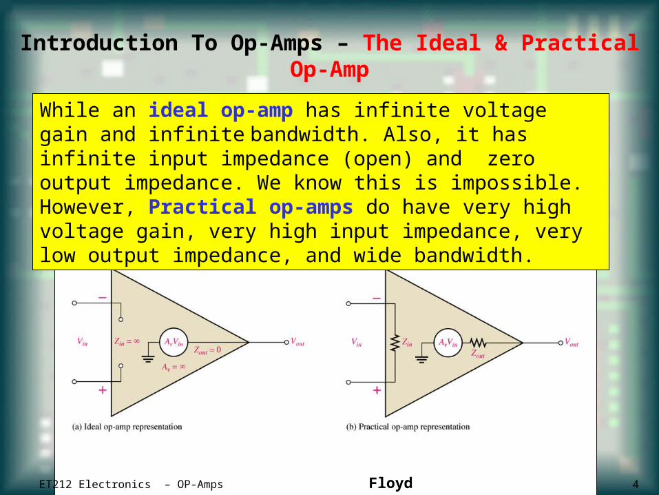
Introduction To Op-Amps – The Ideal & Practical Op-Amp
While an ideal op-amp has infinite voltage gain and infinite bandwidth. Also, it has infinite input impedance (open) and zero output impedance. We know this is impossible. However, Practical op-amps do have very high voltage gain, very high input impedance, very low output impedance, and wide bandwidth.
ET212 Electronics – OP-Amps Floyd 4
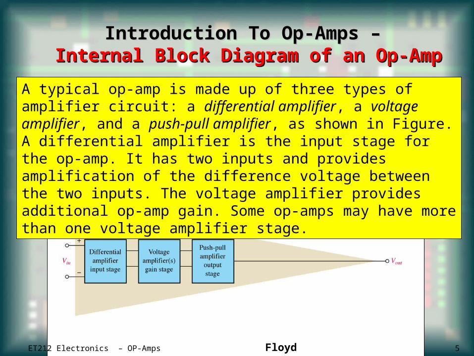
Introduction To Introduction To Op-Amps – Op-Amps – Internal Block Diagram of an Op-AmpInternal Block Diagram of an Op-Amp
A typical op-amp is made up of three types of amplifier circuit: a differential amplifier, a voltage amplifier, and a push-pull amplifier, as shown in Figure. A differential amplifier is the input stage for the op-amp. It has two inputs and provides amplification of the difference voltage between the two inputs. The voltage amplifier provides additional op-amp gain. Some op-amps may have more than one voltage amplifier stage.
ET212 Electronics – OP-Amps Floyd 5

Op-Amp Input Modes and Parameters – Input Signal Modes – Signal-Ended Input
When an op-amp is operated in the single-ended mode, one input is grounded and signal voltage is applied only to the other input as shown in Figure. In the case where the signal voltage is applied to the inverting input as in part (a), an inverted, amplified signal voltage appears at the output. In the case where the signal voltage is applied to the noninverting input with the inverting input grounded, as in part (b), a noninverted, amplified signal voltage appears at the output.
ET212 Electronics – OP-Amps Floyd 6
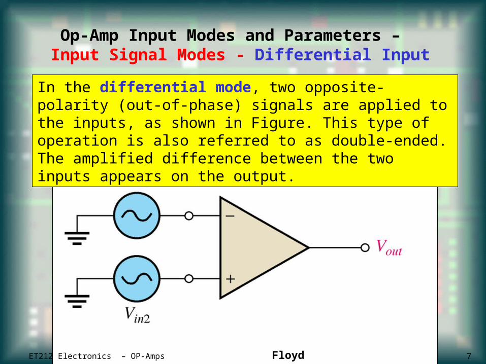
Op-Amp Input Modes and Parameters – Input Signal Modes - Differential Input
In the differential mode, two opposite-polarity (out-of-phase) signals are applied to the inputs, as shown in Figure. This type of operation is also referred to as double-ended. The amplified difference between the two inputs appears on the output.
ET212 Electronics – OP-Amps Floyd 7

Op-Amp Input Modes and Parameters – Input Signal Modes - Common-Mode Input
In the common mode, two signal voltages of the same phase, frequency, and amplitude are applied to the two inputs, as shown in Figure. When equal input signals are applied to both inputs, they cancel, resulting in a zero output voltage. This action is called common-mode rejection.
ET212 Electronics – OP-Amps Floyd 8
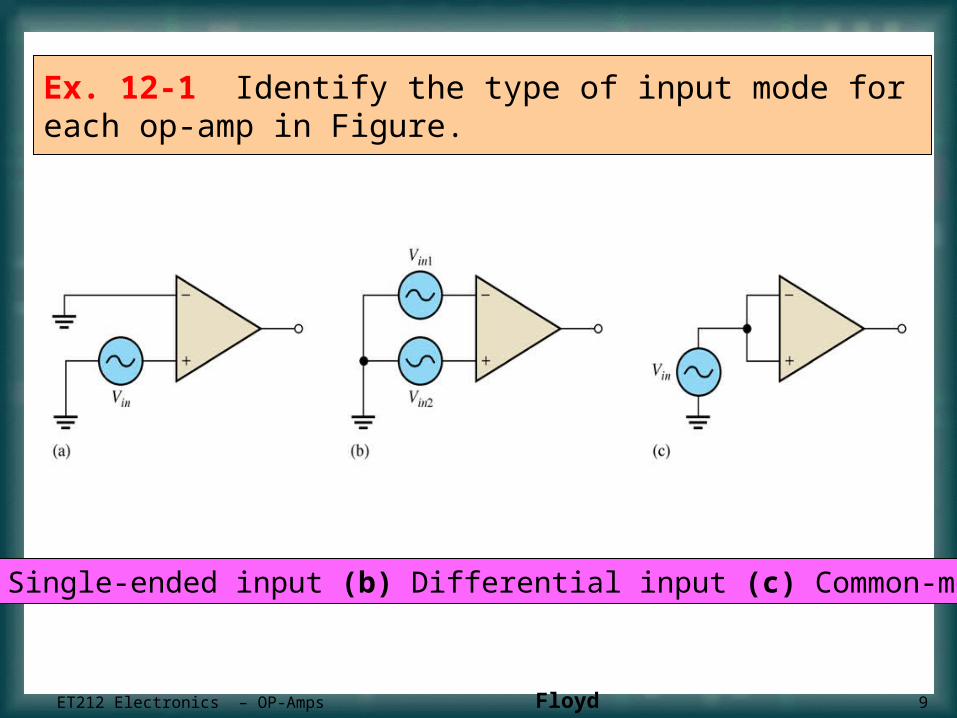
Ex. 12-1 Identify the type of input mode for each op-amp in Figure.
(a) Single-ended input (b) Differential input (c) Common-mode
ET212 Electronics – OP-Amps Floyd 9
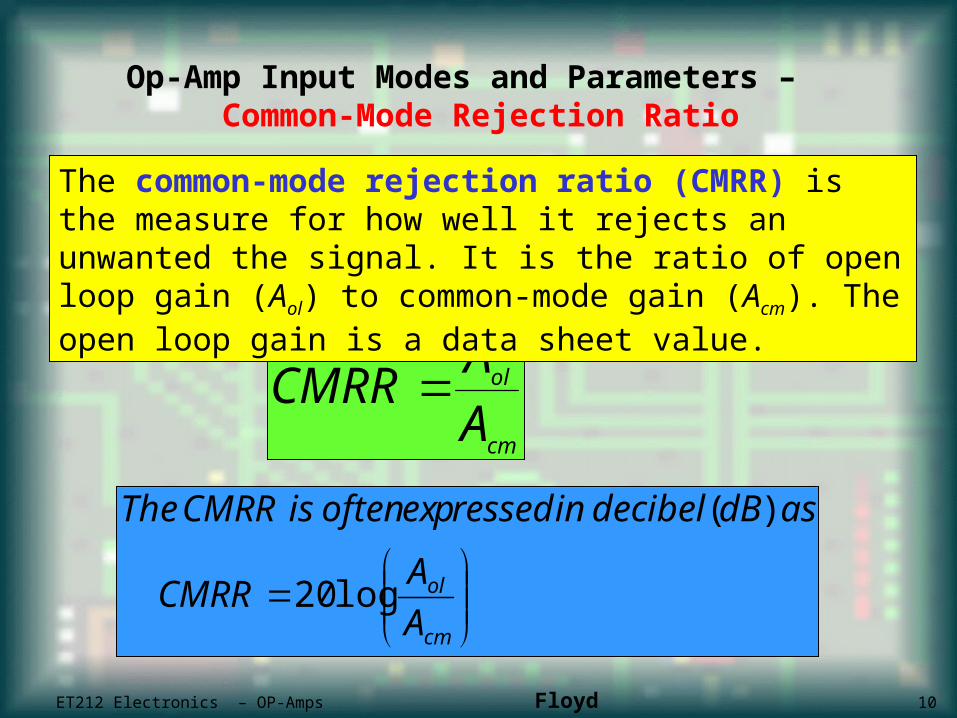
Op-Amp Input Modes and Parameters – Common-Mode Rejection Ratio
cm
ol
A
ACMRR
The common-mode rejection ratio (CMRR) is the measure for how well it rejects an unwanted the signal. It is the ratio of open loop gain (Aol) to common-mode gain (Acm). The open loop gain is a data sheet value.
cm
ol
A
ACMRR
asdBdecibelinressedpexoftenisCMRRThe
log20
)(
ET212 Electronics – OP-Amps Floyd 10

Ex. 12-2 A certain op-amp has an open-loop voltage gain of 100,000 and a common-mode gain of 0.2. Determine the CMRR and express it in decibel.
Aol = 100,000, and Acm = 0.2. Therefore,
Expressed in decibels,
000,5002.0000,100
cm
ol
AA
CMRR
dBCMRR 114)000,500log(20
Ex. 12-3 An op-amp data sheet specifies a CMRR of 300,000 and an Aol of 90,000. What is the common-mode gain?
3.0000,300
000,90
CMRR
AA ol
cm
ET212 Electronics – OP-Amps Floyd 11
Op-Amp Input Modes and Op-Amp Input Modes and ParametersParameters
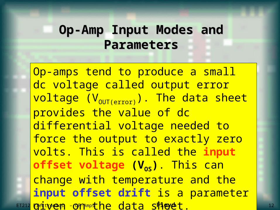
Op-amps tend to produce a small dc voltage called output error voltage (VOUT(error)). The data sheet provides the value of dc differential voltage needed to force the output to exactly zero volts. This is called the input offset voltage (VOS). This can change with temperature and the input offset drift is a parameter given on the data sheet.
ET212 Electronics – OP-Amps Floyd 12
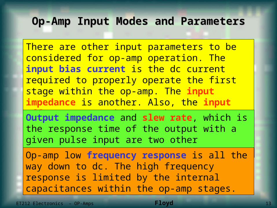
Op-Amp Input Modes and ParametersOp-Amp Input Modes and Parameters
There are other input parameters to be considered for op-amp operation. The input bias current is the dc current required to properly operate the first stage within the op-amp. The input impedance is another. Also, the input offset current which can become a problem if both dc input currents are not the same.
Output impedance and slew rate, which is the response time of the output with a given pulse input are two other parameters.
Op-amp low frequency response is all the way down to dc. The high frequency response is limited by the internal capacitances within the op-amp stages.
ET212 Electronics – OP-Amps Floyd 13
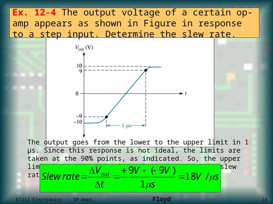
The output goes from the lower to the upper limit in 1 μs. Since this response is not ideal, the limits are taken at the 90% points, as indicated. So, the upper limit is +9 V and the lower limit is -9 V. The slew rate is
sVs
VV
t
VrateSlew out
/18
1
)9(9
Ex. 12-4 The output voltage of a certain op-amp appears as shown in Figure in response to a step input. Determine the slew rate.
ET212 Electronics – OP-Amps Floyd 14
Negative Feedback
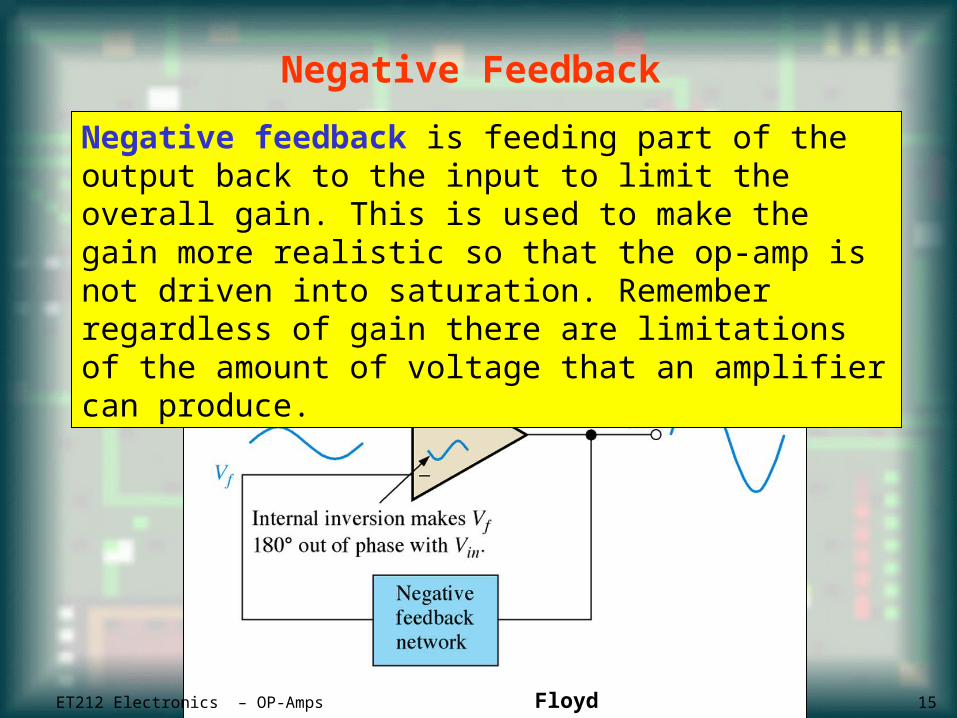
Negative feedback is feeding part of the output back to the input to limit the overall gain. This is used to make the gain more realistic so that the op-amp is not driven into saturation. Remember regardless of gain there are limitations of the amount of voltage that an amplifier can produce.
ET212 Electronics – OP-Amps Floyd 15
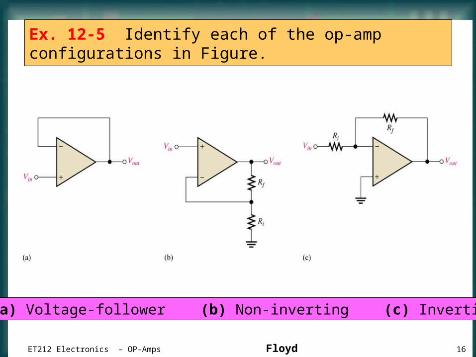
Ex. 12-5 Identify each of the op-amp configurations in Figure.
(a) Voltage-follower (b) Non-inverting (c) Inverting
ET212 Electronics – OP-Amps Floyd 16

Op-Amps With Negative Feedback – noninverting Amplifier
011
f
out
i R
VV
R
V
0 outinifin VVRRV
V2
V1
ini
fin
fiout
outifiin
VR
RV
R
RRV
VRRRV
)1(
)(
The closed-loop voltage gain (Acl) is the voltage gain of an op-amp with external feedback. The gain can be controlled by external component values. Closed loop gain for a non-inverting amplifier can be determined by the formula below.
Ideal Op-AmpV1 = V2 = Vin
ET212 Electronics – OP-Amps Floyd 17
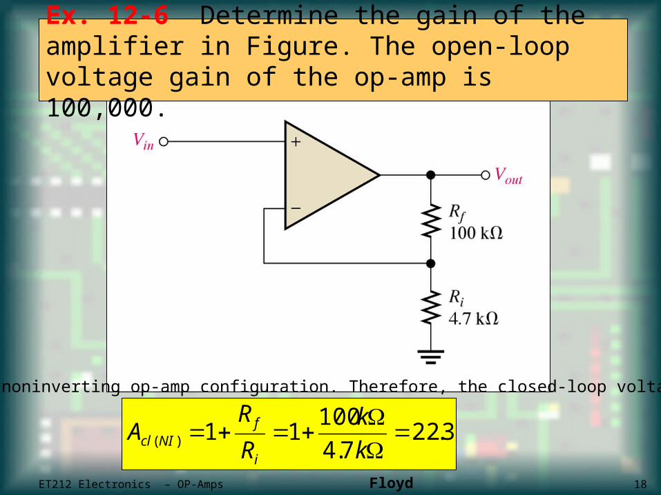
This is a noninverting op-amp configuration. Therefore, the closed-loop voltage gain is
3.227.4
10011)(
k
k
R
RA
i
fNIcl
Ex. 12-6 Determine the gain of the amplifier in Figure. The open-loop voltage gain of the op-amp is 100,000.
ET212 Electronics – OP-Amps Floyd 18
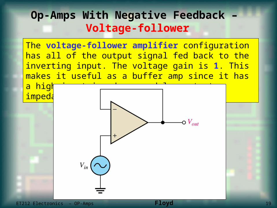
Op-Amps With Negative Feedback – Voltage-follower
The voltage-follower amplifier configuration has all of the output signal fed back to the inverting input. The voltage gain is 1. This makes it useful as a buffer amp since it has a high input impedance and low output impedance.
ET212 Electronics – OP-Amps Floyd 19

Op-Amps With Negative Feedback –Inverting Amplifier
011
f
out
i
in
R
VV
R
VV
V1
V2
ini
fout
ioutfin
VR
RV
RVRV
0
The inverting amplifier has the output fed back to the inverting input for gain control. The gain for the inverting op-amp can be determined by the formula below.
Ideal Op-Amp
V1 = V2 = 0
ET212 Electronics – OP-Amps Floyd 20

kkRAR
R
RA
iIclf
i
f
Icl
220)2.2)(100()(
)(
Ex. 12-7 Given the op-amp configuration in Figure, determine the value of Rf required to produce a closed-loop voltage gain of -100.
21
Knowing that Ri = 2.2 kΩ and the absolute value of the closed-loop gain is |Acl(I)| = 100, calculate Rf as follows:
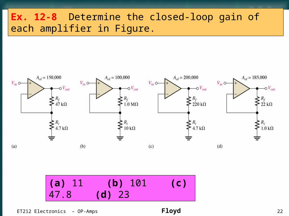
Ex. 12-8 Determine the closed-loop gain of each amplifier in Figure.
(a) 11 (b) 101 (c) 47.8 (d) 23
ET212 Electronics – OP-Amps Floyd 22
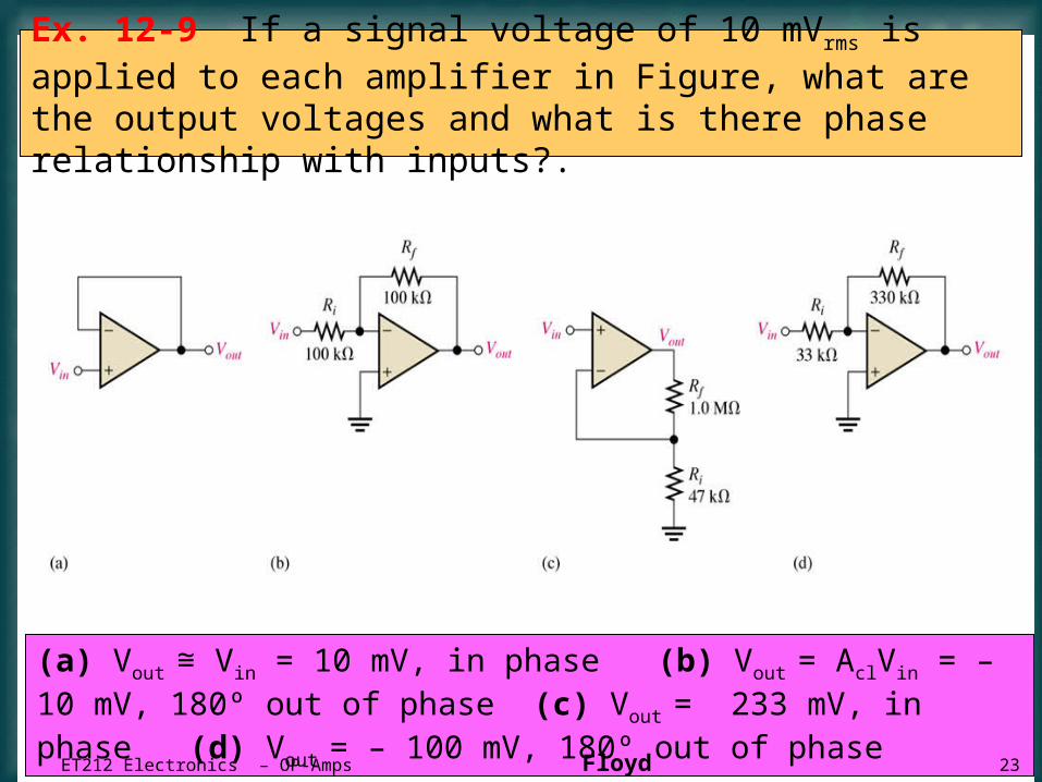
Ex. 12-9 If a signal voltage of 10 mVrms is applied to each amplifier in Figure, what are the output voltages and what is there phase relationship with inputs?.
(a) Vout ≅ Vin = 10 mV, in phase (b) Vout = AclVin = – 10 mV, 180º out of phase (c) Vout = 233 mV, in phase (d) Vout = – 100 mV, 180º out of phase
ET212 Electronics – OP-Amps Floyd 23
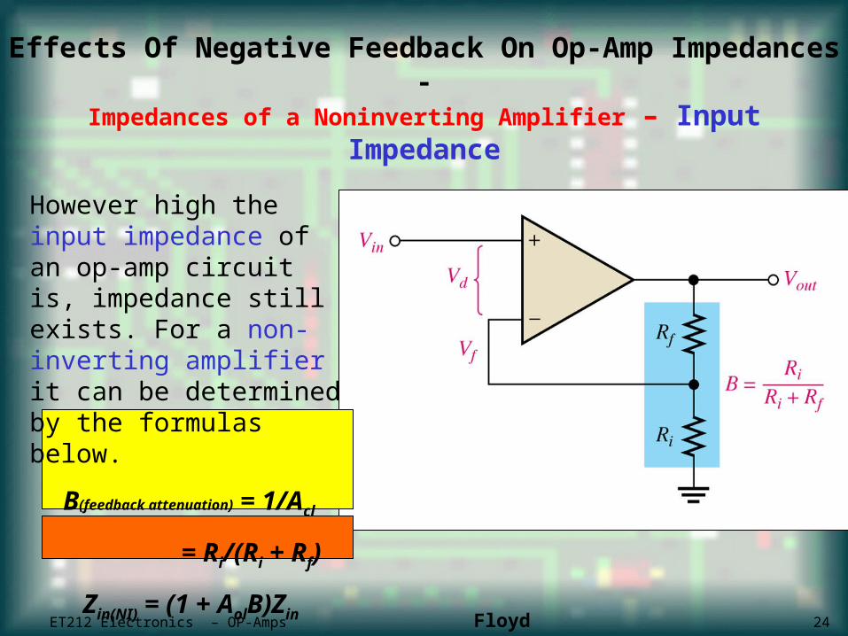
Effects Of Negative Feedback On Op-Amp Impedances -
Impedances of a Noninverting Amplifier – Input Impedance
However high the input impedance of an op-amp circuit is, impedance still exists. For a non-inverting amplifier it can be determined by the formulas below.
B(feedback attenuation) = 1/Acl
= Ri/(Ri + Rf)
Zin(NI) = (1 + AolB)Zin
ET212 Electronics – OP-Amps Floyd 24
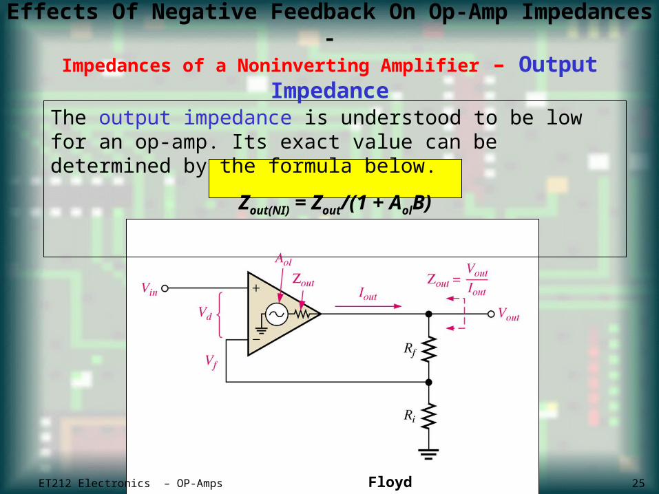
The output impedance is understood to be low for an op-amp. Its exact value can be determined by the formula below.
Zout(NI) = Zout/(1 + AolB)
Effects Of Negative Feedback On Op-Amp Impedances -
Impedances of a Noninverting Amplifier – Output Impedance
ET212 Electronics – OP-Amps Floyd 25
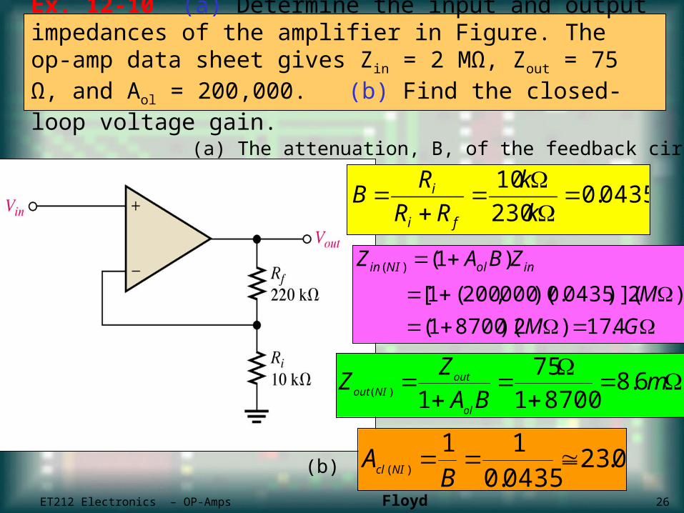
Ex. 12-10 (a) Determine the input and output impedances of the amplifier in Figure. The op-amp data sheet gives Zin = 2 MΩ, Zout = 75 Ω, and Aol = 200,000. (b) Find the closed-loop voltage gain.
0435.0230
10
k
k
RR
RB
fi
i
GM
M
ZBAZ inolNIin
4.17)2)(87001(
)2)](0435.0)(000,200(1[
)1()(
(a) The attenuation, B, of the feedback circuit is
mBA
ZZ
ol
outNIout 6.8
8700175
1)(
0.230435.011
)( B
A NIcl(b)
ET212 Electronics – OP-Amps Floyd 26

Ex. 12-11 The same op-amp in Example 6-10 is used in a voltage-follower configuration. Determine the input and output impedance.
GMZAZ
BSince
inolVFin 400)2)(000,2001()1(
,1
)(
375
000,2001
75
1)(ol
outVFout A
ZZ
Notice that Zin(VF) is much greater than Zin(NI), and Zout(VF) is much less than Zout(NI) from Example 6-10.
ET212 Electronics – OP-Amps Floyd 27
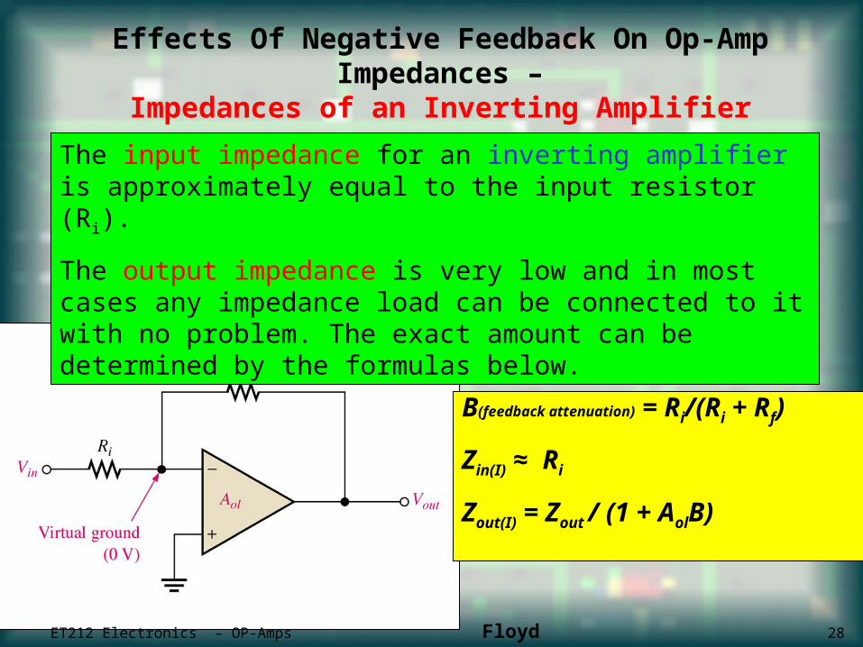
B(feedback attenuation) = Ri/(Ri + Rf)
Zin(I) ≈ Ri
Zout(I) = Zout / (1 + AolB)
Effects Of Negative Feedback On Op-Amp Impedances –
Impedances of an Inverting Amplifier
The input impedance for an inverting amplifier is approximately equal to the input resistor (Ri).
The output impedance is very low and in most cases any impedance load can be connected to it with no problem. The exact amount can be determined by the formulas below.
ET212 Electronics – OP-Amps Floyd 28

Ex. 12-12 Find the value of the input and output impedances in Figure. Also, determine the closed-loop voltage gain. The op-amp has the following parameters: Aol = 50,000; Zin = 4 MΩ; and Zout = 50 Ω.
kRZ iIin 0.1)(
01.0101
0.1
k
k
RR
RB
fi
i
m
BA
ZZ
ol
outIout 99
)01.0)(000,50(1
50
1)(
The feedback attenuation, B, is
Then
The closed-loop voltage gain is (zero for all practical purposes)
1000.1
100)(
k
k
R
RA
i
fIcl
ET212 Electronics – OP-Amps Floyd 29

ET212 Electronics – OP-Amps Floyd 30
3 dB 3 dB Open-Loop ResponseOpen-Loop Response
The open-loop gain of an op-amp is determined by the internal design and it very high. The high frequency cutoff frequency of an open-loop op-amp is about 10 Hz.
Ideal plot of open-loop voltage gain versus frequency for a typical op-amp. The frequency scale is logarithmic.
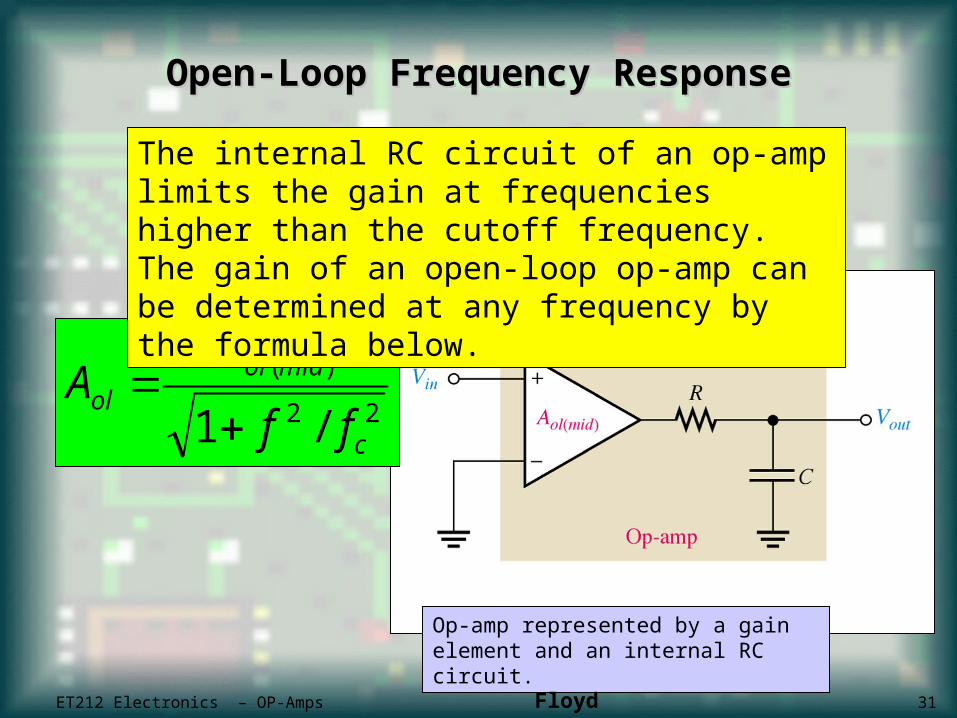
Open-Loop Open-Loop Frequency Frequency ResponseResponse
Op-amp represented by a gain element and an internal RC circuit.
22
)(
/1 c
midolol
ff
AA
The internal RC circuit of an op-amp limits the gain at frequencies higher than the cutoff frequency. The gain of an open-loop op-amp can be determined at any frequency by the formula below.
ET212 Electronics – OP-Amps Floyd 31
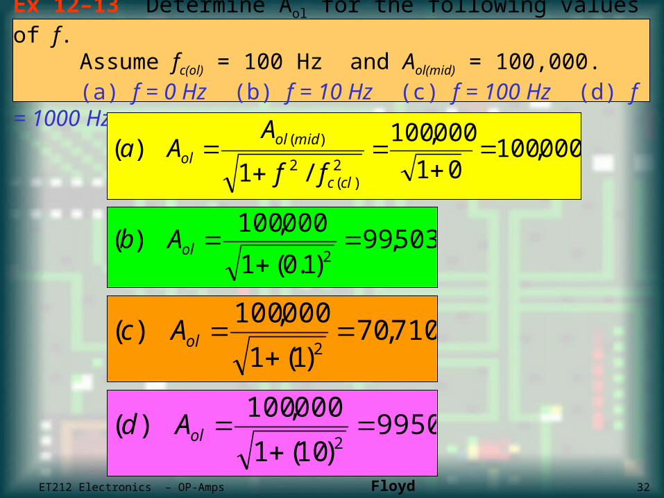
Ex 12–13 Determine Aol for the following values of f. Assume fc(ol) = 100 Hz and Aol(mid) = 100,000.(a) f = 0 Hz (b) f = 10 Hz (c) f = 100 Hz (d) f = 1000 Hz
000,10001
000,100
/1)(
2)(
2
)(
clc
midolol
ff
AAa
503,99)1.0(1
000,100)(
2
olAb
710,70)1(1
000,100)(
2
olAc
9950)10(1
000,100)(
2
olAd
ET212 Electronics – OP-Amps Floyd 32

Open-Loop ResponseOpen-Loop Response – – Phase ShiftPhase Shift
Of course as with any RC circuit phase shift begins to occur at higher frequencies. Remember we are viewing internal characteristics as external components.
cf
fShiftPhase 1tan)(
ET212 Electronics – OP-Amps Floyd 33
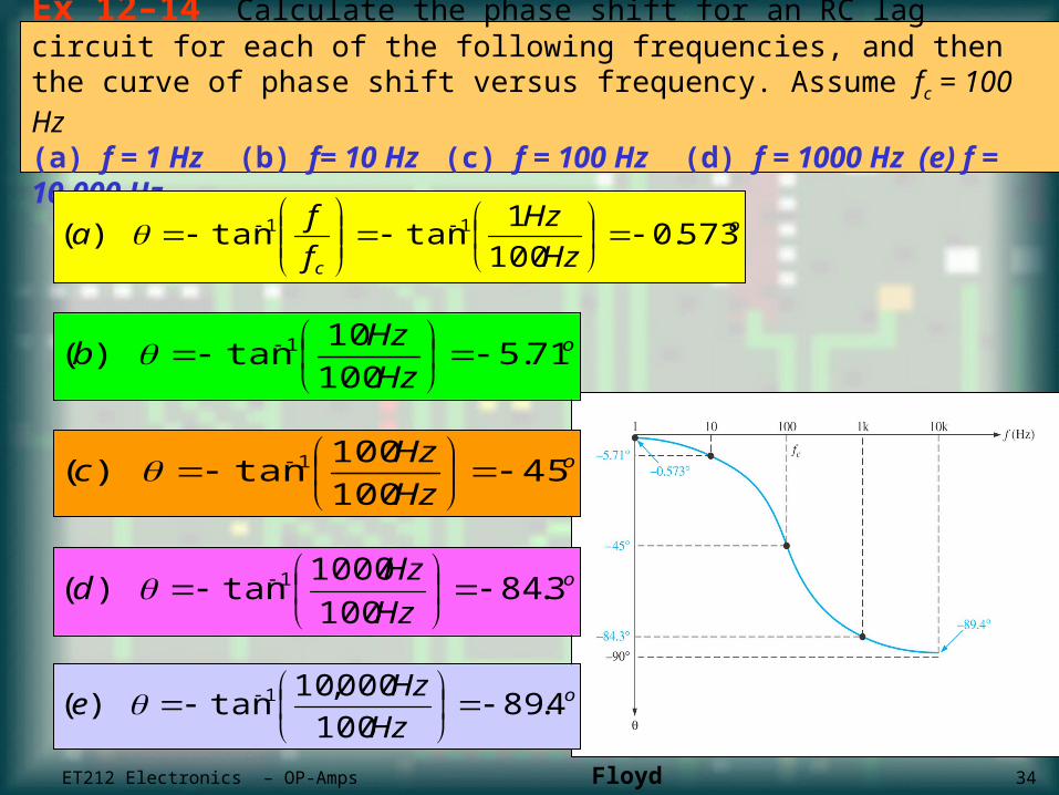
Ex 12–14 Calculate the phase shift for an RC lag circuit for each of the following frequencies, and then the curve of phase shift versus frequency. Assume fc = 100 Hz(a) f = 1 Hz (b) f= 10 Hz (c) f = 100 Hz (d) f = 1000 Hz (e) f = 10,000 Hz
o
c Hz
Hz
f
fa 573.0
100
1tantan)( 11
o
Hz
Hzb 71.5
100
10tan)( 1
o
Hz
Hzc 45
100
100tan)( 1
o
Hz
Hzd 3.84
100
1000tan)( 1
o
Hz
Hze 4.89
100
000,10tan)( 1
ET212 Electronics – OP-Amps Floyd 34
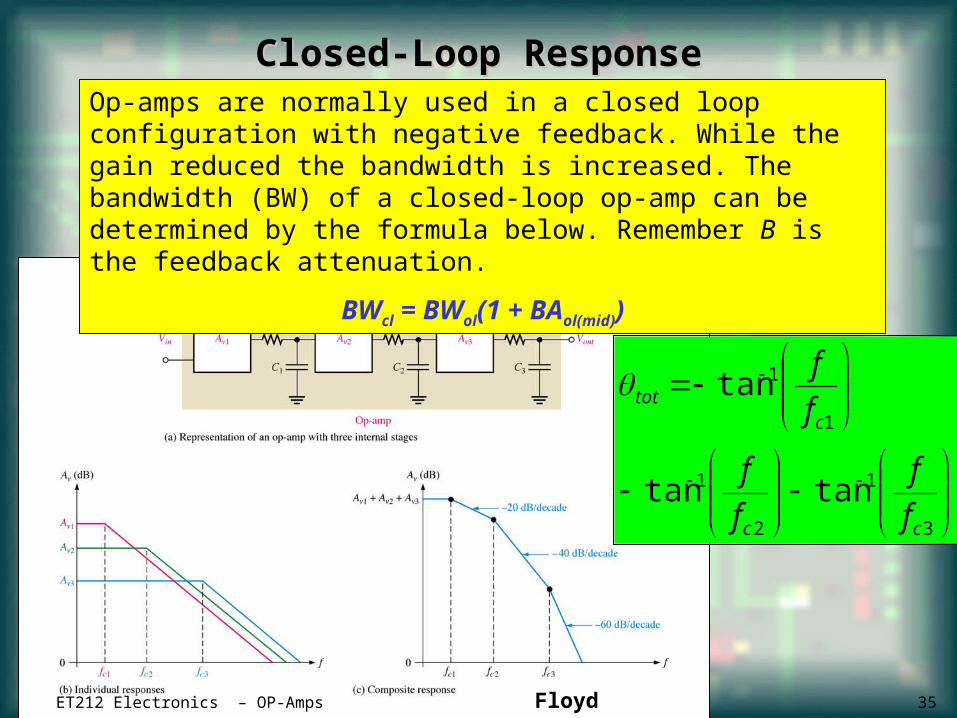
Closed-Loop ResponseClosed-Loop ResponseOp-amps are normally used in a closed loop configuration with negative feedback. While the gain reduced the bandwidth is increased. The bandwidth (BW) of a closed-loop op-amp can be determined by the formula below. Remember B is the feedback attenuation.
BWcl = BWol(1 + BAol(mid))
3
1
2
1
1
1
tantan
tan
cc
ctot
f
f
f
f
f
f
ET212 Electronics – OP-Amps Floyd 35
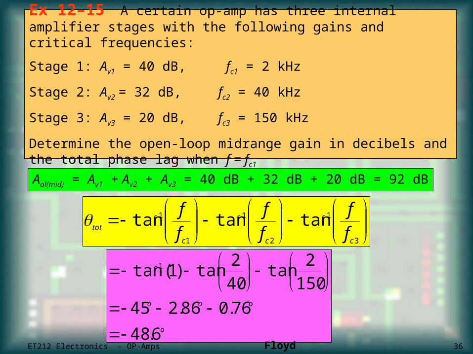
Ex 12–15 A certain op-amp has three internal amplifier stages with the following gains and critical frequencies:
Stage 1: Av1 = 40 dB, fc1 = 2 kHz
Stage 2: Av2 = 32 dB, fc2 = 40 kHz
Stage 3: Av3 = 20 dB, fc3 = 150 kHz
Determine the open-loop midrange gain in decibels and the total phase lag when f = fc1
3
1
2
1
1
1 tantantanccc
tot f
f
f
f
f
f
Aol(mid) = Av1 + Av2 + Av3 = 40 dB + 32 dB + 20 dB = 92 dB
o
ooo
6.48
76.086.245
1502
tan402
tan)1(tan 1
ET212 Electronics – OP-Amps Floyd 36
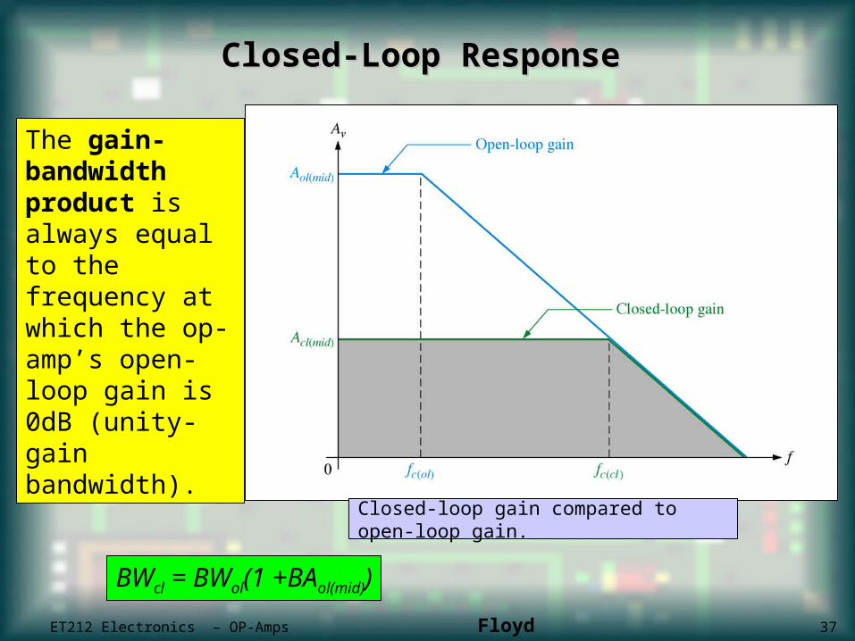
Closed-Loop ResponseClosed-Loop Response
The gain-bandwidth product is always equal to the frequency at which the op-amp’s open-loop gain is 0dB (unity-gain bandwidth).
BWcl = BWol(1 +BAol(mid))
Closed-loop gain compared to open-loop gain.
ET212 Electronics – OP-Amps Floyd 37
Related Documents