OpenPit OpenPiton FPGA Prototype Manual Wentzlaff Parallel Research Group Princeton University [email protected] Version 3.0

Welcome message from author
This document is posted to help you gain knowledge. Please leave a comment to let me know what you think about it! Share it to your friends and learn new things together.
Transcript

OpenPit
OpenPiton FPGA Prototype Manual
Wentzlaff Parallel Research Group
Princeton University
Version 3.0

Revision History
Revision Date Author(s)Description
1.0 06/30/15 AL Initial version2.0 2/29/16 AL Added support VC707,
Genesys2 and NexysVideodevelopment boards
2.1 4/2/16 MM,AL SD boot image generation.Porting to another boards.Debugging and Simulation.
2.5 10/19/16 AL Described UART DMW. Re-moved BRAM OBP. New lo-cation of FPGA specific files.
3.0 3/22/17 KL, AL Added details on networksupport and updated figuresaccording to new chipset de-sign. Updated boards’ fre-quencies. Decribed oled,port options for tools.
3.1 6/9/17 JB Simplified ramdisk gener-ation to remove bespokescript. Added recommenda-tion to use our images ratherthan creating a new one.
ii

Contents
1 Preface 1
1.1 Notation Conventions . . . . . . . . . . . . . . . . 1
1.2 Supported Tools and Environment Set Up . . . . 1
1.2.1 SW Requirements . . . . . . . . . . . . . . 1
1.2.2 HW Requirements . . . . . . . . . . . . . 3
1.2.3 Job Queue Managers . . . . . . . . . . . . 3
2 Introduction 4
3 Prototype Architecture 5
3.1 Top Level Architecture . . . . . . . . . . . . . . . 5
3.2 IO_CTRL_TOP Architecture . . . . . . . . . . . 6
4 Mapping of a Processor to FPGA 9
4.1 Mapping of Processor’s SRAMs . . . . . . . . . . 10
4.2 Mapping of Main Memory . . . . . . . . . . . . . 10
4.2.1 Using on-Board DDR3 Memory . . . . . . 11
4.2.2 Memory Emulation With on-FPGA BRAMs 11
4.2.3 Memory Emulation With SD Card . . . . 12
5 Design Configurations and Tools 13
5.1 Prototype Project Defines . . . . . . . . . . . . . 13
5.2 Prototype Configurations . . . . . . . . . . . . . . 14
5.3 Running Implementation for Supported Develop-ment Boards . . . . . . . . . . . . . . . . . . . . . 15
5.4 Memory Address Spaces for Different PrototypeConfigurations . . . . . . . . . . . . . . . . . . . . 16
iii

6 Prototype Operation 18
6.1 Reset Sequence . . . . . . . . . . . . . . . . . . . 18
6.2 Loading Assembly Tests from PC to DDR . . . . 18
6.3 Assembly Test Execution . . . . . . . . . . . . . . 19
6.4 Booting OS from an SD Card . . . . . . . . . . . 19
7 Simulation and Debugging 21
7.1 Software Simulation from Vivado . . . . . . . . . 21
7.2 Inserting Debug Cores for Logic Analyzer . . . . . 21
8 Description and Structure of Prototype SpecificFiles and Scripts 23
8.1 Source Files and Scripts . . . . . . . . . . . . . . 23
8.1.1 Synthesis and Implementation Files . . . . 23
8.2 Generated Files . . . . . . . . . . . . . . . . . . . 24
9 Networking 25
9.1 Interrupts . . . . . . . . . . . . . . . . . . . . . . 25
9.2 Bringing up the network interface . . . . . . . . . 25
A protosyn manpage 26
B pitonstream manpage 28
C pitonunimap manpage 29
D .ustr file format 30
E Porting OpenPiton Prototype to a Custom Devel-opment Board 31
F Step-by-Step Instructions for Booting DebianLinux and Playing Tetris 35
iv
G Generating an SD-Bootable Image 37
G.1 Building a Ramdisk from Scratch . . . . . . . . . 37
G.1.1 Initialization . . . . . . . . . . . . . . . . . 37
G.1.2 Mounting and Filling the Disk . . . . . . . 38
G.2 Modifying an Existing Ramdisk . . . . . . . . . . 40
G.3 Creating an SD Image . . . . . . . . . . . . . . . 41
References 42
v

List of Figures
1 Top level prototype architecture with a defaultconfiguration. FPGA pins are shown as greenrectangles and are connected to logical signals atsystem module. . . . . . . . . . . . . . . . . . . . 5
2 Architecture of the io_ctrl_top module. Labelsfor arrows represent interface and NOC types. . . 8
3 Memory blocks and their sizes inside an Open-Piton tile . . . . . . . . . . . . . . . . . . . . . . 11
4 $MODEL_DIR directory structure . . . . . . . . 24
5 Genesys2 board running Tetris on full stack De-bian Linux . . . . . . . . . . . . . . . . . . . . . . 36
vi

List of Tables
1 Notation conventions . . . . . . . . . . . . . . . . 1
2 Supported development boards and their parameters 4
3 Suggested prototype configurations (OS_SD,BRAM_TEST and UART_DMW DDR) with in-frastructure blocks included into them . . . . . . 15
4 Steps of protosyn run for some of its options . . 16
vii

Example Description$DV_ROOT/tools/src/proto Italic text is used to indicate
paths to scripts and folderssource add_files.tcl Courier font is used for com-
mands, scripts’ names, IP corenames and file names
NEXYSVIDEO_BOARD Text in all capital COURIER fontis used for defines
Tcl Console Capitalized text is used formenu options
Note: Any text in bold is used tohighlight a special topic or par-ticular option
Table 1: Notation conventions
1 Preface
1.1 Notation Conventions
Text conventions used in the manual are specified in Table 1.
1.2 Supported Tools and Environment Set Up
1.2.1 SW Requirements
• In order to be able to run scripts, $DV_ROOT and$MODEL_DIR environment variables should be defined.They can be set by moving to the topmost directory ofOpenPiton framework folder, and executing the followingcommands:
export PITON_ROOT=$PWDsource piton/piton_settings.bash
• To be able to run FPGA implementation of OpenPitonFPGA prototype, Xilinx Vivado tool should be installedon a development machine. For this release Vivado 2015.4version has been tested and is supported. You can checkVivado version by runningvivado -version
1
• For loading tests from a PC through UART on FPGA thenext requirements should be met:
1. Python used on PC should have pyserial library in-stalled.
2. Depending on the OS used, it could be requiredto recompile configsrch script (sources located in$DV_ROOT/tools/src/proto/configsrch). Runmake; make installto compile and install configsrch for your system.In addition to the above step, you could have to in-stall required Perl packages used by the tools. InUbuntu you can run perlpkg.sh script located in$DV_ROOT/tools/src/proto to do this. For othersystems, list of additional packages can be taken fromthe script and installed according to the system.
3. Support for 32-bit programs should be enabled andlibraries should be installed. On Ubuntu, run thenext commands:dpkg –add-architecture i386apt-get updateapt-get install libc6:i386 libncurses5:i386libstdc++6:i386apt-get clean && apt-get update && apt-getupgradeapt-get install -f
4. Install the 32-bit version of gmp. On Ubuntu run:wget http://mirrors.kernel.org/ubuntu/pool/universe/g/gmp4/libgmp3c2_4.3.2+dfsg-2ubuntu1_i386.deb;dpkg -i libgmp3c2_4.3.2+dfsg-2ubuntu1_i386.deb
All the above steps can be run on Ubuntu using$DV_ROOT/tools/src/proto/syscfg.sh script. This scriptcan also be used as a reference for other OSes.
• Current implementation of processor memory on BRAMsimplies that some tests should be run in SW simulatorfirst. The Synopsys VCS program has to be installed (seeSimulation Manual Section 2.5.2 Verilog Simulator for moredetails).
2

1.2.2 HW Requirements
You need one of a supported development boards, listed in Ta-ble 2. If configuration implies usage of an SD card, you will needone micro SD. Because of SD controller limitations, only microSDSC cards are supported (not SDHC).
1.2.3 Job Queue Managers
SLURM (Simple Linux Utility for Resource Management) is op-tional protosyn script supports using it via --slurm commandoption. Currently, SLURM version 15.08.8 has been tested with.
3

Development Board,FPGA name,Part Number
Core Clock(1 core)
Max#
Cores
DDR type,Size,
Data widthXilinx VC707
Virtex-7XC7VX485T-2FFG1761C
60 MHz 3DDR31GB64 bits
Digilent Genesys2Kintex-7
XC7K325T-2FFG900C66.667 MHz 2
DDR31GB32 bits
Digilent NexysVideoArtix-7
XC7A200T-1SBG484C30 MHz 1
DDR3512MB16 bits
Table 2: Supported development boards and their parameters
2 Introduction
High speed and relatively low price of FPGAs make them themost common choice for hardware/software interface verificationof a processor design. However, design bring-up time, limited ca-pacity of logic cells and width of external interfaces can introduceadditional challenges during prototyping step of a project flow[1].
In order to speed up prototyping of a processor and enable aflexible framework for hardware/software interface verification,the FPGA prototype for OpenPiton processor [2] is publicly re-leased. It targets several development boards with Xilinx FP-GAs. The release includes all scripts required to implementOpenPiton from Verilog sources down to bit files to programan FPGA. In addition, all the changes applied to a design toenable FPGA synthesis are described, so it can be easily portedto other development boards and FPGAs.
Because of limited FPGA capacity at most three processor tilesfit on one VC707 development board [3]. For all currently sup-ported development boards, maximum number of cores fittingon them, and core clock frequencies see Table 2.
4
CLK MMC
M
VA
L_T
O_C
RE
DIT
CR
ED
IT_T
O_V
AL
IO_CTRL_TOP
SYSTEM
ME
M_I
O_S
PL
ITT
ER
MC_TOP
spi_*
clk_
p
clk_
n
sys_
rst
...DD
Rin
terf
ace
pin_tx
pin_rx
uar
t_b
oo
t_en
CHIPSET
net_phy_*
MD
IO
Co
re
Co
re
Co
re
Co
re
CHIP
DRAM
UART
ETH
SD
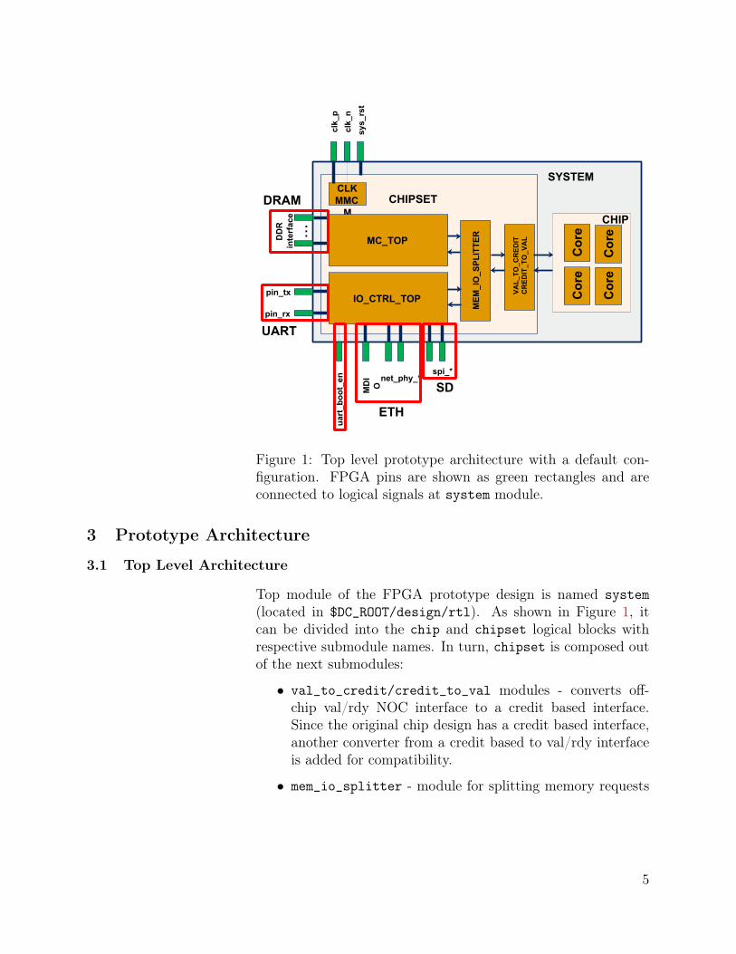
Figure 1: Top level prototype architecture with a default con-figuration. FPGA pins are shown as green rectangles and areconnected to logical signals at system module.
3 Prototype Architecture
3.1 Top Level Architecture
Top module of the FPGA prototype design is named system(located in $DC_ROOT/design/rtl). As shown in Figure 1, itcan be divided into the chip and chipset logical blocks withrespective submodule names. In turn, chipset is composed outof the next submodules:
• val_to_credit/credit_to_val modules - converts off-chip val/rdy NOC interface to a credit based interface.Since the original chip design has a credit based interface,another converter from a credit based to val/rdy interfaceis added for compatibility.
• mem_io_splitter - module for splitting memory requests
5
from a chip to DDR memory and IO controller1.
• io_ctrl_top - top module for external IO controllers(UART and SD card* by this moment). It has an internalsplitter to direct memory requests to a correct IO deviceand arbitrate between responses2.
• mc_top - a top level for a memory controller. Because ofthe application side of the MIG 7 IP core working at ahigher frequency than the chip and having an interfacedifferent from NOC’s val/rdy, asynchronous FIFOs andpacket transceivers are required. Width of DDR data busdepends on a board type (see Table 2), therefore memorycontroller was designed to have a configurable applicationdata interface to MIG 7 IP core. As a result, the numberof cycles required to read/write one cache line varies fromboard to board.
• clk_mmcm - Xilinx’s IP core for clock generation.
Pins shown in Figure 1 as green rectangles are self-explanatory.Input pin uart_boot_en is connected to the last SW7 on eachFPGA board, which is used to control whether if the system iswaiting for a test to be loaded through UART or starts bootingLinux from SD card. Depending on the board type, clk_n/clk_ppin pair can be a single ended clock or not.
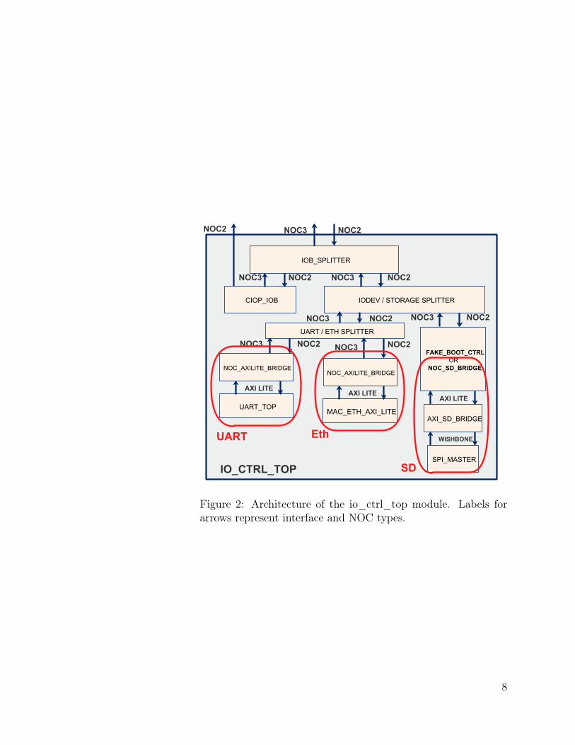
3.2 IO_CTRL_TOP Architecture
Architecture of io_ctrl_top module is shown in Figure 2. Ituses NOC1, NOC2 and NOC3 interfaces for communication withthe chip, SPI interface to communicate with SD card (not shownon the Figure), uart_tx/uart_rx interface to communicate witha host PC through UART, and additional control signals to checktest completion conditions (not shown). Its subblocks are de-scribed below:
• iob_splitter - module which splits requests from coresbetween I/O devices and ciop_iob
1 This is not the same as splitting the IO space and main memory. Seeprecise description of its operation for different project configurations inSection 5.4
2 The presence of an SD card controller depends on project configuration.See Section 5.1
6
• ciop_iob - module which sends interrupts to cores throughNOC2. Among other interrupts, the module send a wake-up packet to a core (see reset sequence in Section 6.1). Thismodule is also responsible for sending network interruptpackets to the core when they are enabled
• iodev_storage_splitter - splits memory requests be-tween I/O devices and chipset storage memory spaces.
• uart_eth_splitter - splits memory requests betweenUART and Eth memory spaces. UART memory spaceshould be the same as configured in the Hypervisor or as-sembly test.
• noc_axilite_bridge, uart_top - bridge and top levelUART module. uart_top contains logic processing bitstream from PC when loading a test into DDR and sendscontrol sequences after each test completion.
• noc_axilite_bridge, mac_eth_axi_lite - bridge andEthernet Lite MAC IP core. There is also an externalconverter from RGMII interface of IP core to MII interfaceof PHY chip on Genesys2 and NexysVideo boards.
• fake_boot_ctrl - module with a BRAM containing an as-sembly test in case of protosyn was run with --bram-testoption.
• noc_sd_bridge, axi_sd_bridge, spi_master - modulescomposing SD controller and its interface.
7
CIOP_IOB
IOB_SPLITTER
IODEV / STORAGE SPLITTER
FAKE_BOOT_CTRLOR
NOC_SD_BRIDGE
UART_TOP
AXI_SD_BRIDGE
SPI_MASTER
NOC_AXILITE_BRIDGE
NOC2NOC3
NOC2NOC3NOC2NOC3
NOC2NOC3
NOC2NOC3
AXI LITE
AXI LITE
WISHBONEUART
SDIO_CTRL_TOP
UART / ETH SPLITTER
NOC2NOC3
NOC2NOC3
MAC_ETH_AXI_LITE
NOC_AXILITE_BRIDGE
AXI LITE
Eth
NOC2
Figure 2: Architecture of the io_ctrl_top module. Labels forarrows represent interface and NOC types.
8

4 Mapping of a Processor to FPGA
In order to port processor design on FPGA, its design shouldbe transformed to an identical synthesizable form for a chosenFPGA. On top of that, infrastructure used for simulation shouldbe converted to a synthesizable format as well to allow runningof assembly tests and booting OS on a prototype. These changesrequire removing and/or replacing all of the chip specific modules(like RAMs, phy levels, etc.) with their equivalents supportedby FPGA tools.
The following IP blocks were created specifically for prototypingOpenPiton:
• Block memories to emulate on-chip SRAMs
• Main Memory controller (MIG7 Xilinx IP core)
• Asynchronous FIFOs for inter-clock domain transfers
• Generator of system clocks
• UART16550 - serial interface for communication with hostPC
• MAC for communication with Ethernet PHY chip onGenesys2 and NexysVideo boards
In addition to IP blocks, we designed infrastructure moduleswhich replace and/or extend capabilities of software simulationinfrastructure:
• Main Memory/IO and UART/BOOT splitters
• Converter between NOC interface and Memory controllerinterface with configurable data width
• Converter between NOC interface and SD controller
• A wrapper around UART 16550 IP core for enabling DirectMemory Writes from a host computer
• Multiplexers for choosing a master module for drivingMemory Controller
• Emulation of assembly test memory with BRAMs and cor-responding controllers
• A wrapper around SD card controller
9

For a complete schematic of FPGA design see Figure 1. Fordefines used to configure a project and provided scripts optionssee Section 5.1.
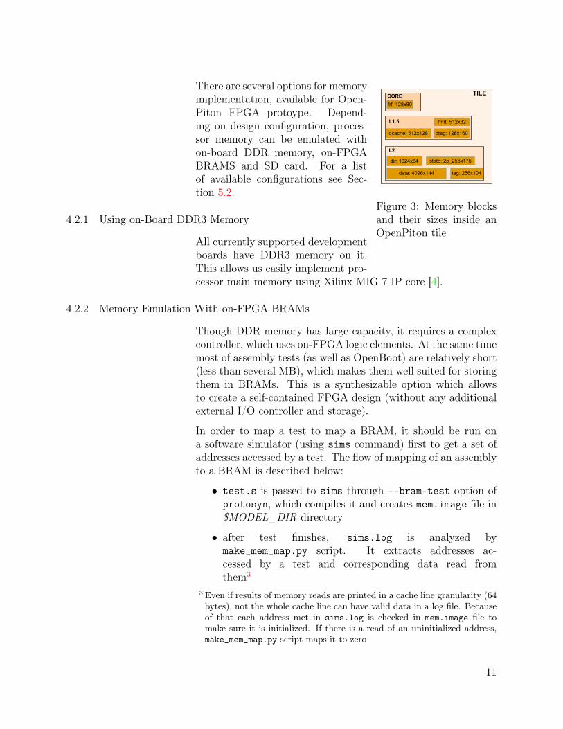
4.1 Mapping of Processor’s SRAMs
OpenPiton has several on-chip SRAMs which are implementedas register arrays for simulation. Some of these memories havebit-enable write masks. Because of IP cores for Xilinx FPGABRAMs can have only byte-enable write mask, we designedwrappers which implement bit-enable write mask functionalityon top of available BRAMs.
SRAMs which are implemented as block memories are shown onFigure 3. All of them except a memory for L2 states (2p_256_176on Figure 3) are simple dual port memories with one read andone write port. For a write request we first read the contentof memory block, perform a bitwise operation based on a maskand write data back to memory in the next cycle. Since originalSRAMs have only one port (with selection of operation type),it guarantees that there is no read conflict when two memoryblocks are read at the same cycle. The only case which requiresa special attention is writing and reading of the same block intwo adjacent cycles. In this case for a read operation we haveto return a result after bitwise operation, not to read it frommemory (because of writes to a BRAM occur one cycle after arequest).
Original SRAM for L2 states is a simple dual-ported memorywith one port for read and one port for write requests. A wrap-per used for it in FPGA design instantiates a true dual-portedmemory because in contrast to above case this memory can haveread conflicts. To enable bit-enable write mask the wrapper padsincoming data and mask bits which always have the same maskwith zeros.
Memory wrappers for BRAMs are located in the$DV_ROOT/design/proto directory.
4.2 Mapping of Main Memory
Simulation infrastructure for OpenPiton implements memory us-ing Verilog PLI. Obviously, this solution can not be used for aprototype because of if is not synthesizable.
10
frf: 128x80
hmt: 512x32L1.5
dtag: 128x160dcache: 512x128
dir: 1024x64
data: 4096x144
state: 2p_256x176
tag: 256x104
L2
TILECORE
Figure 3: Memory blocksand their sizes inside anOpenPiton tile
There are several options for memoryimplementation, available for Open-Piton FPGA protoype. Depend-ing on design configuration, proces-sor memory can be emulated withon-board DDR memory, on-FPGABRAMS and SD card. For a listof available configurations see Sec-tion 5.2.
4.2.1 Using on-Board DDR3 Memory
All currently supported developmentboards have DDR3 memory on it.This allows us easily implement pro-cessor main memory using Xilinx MIG 7 IP core [4].
4.2.2 Memory Emulation With on-FPGA BRAMs
Though DDR memory has large capacity, it requires a complexcontroller, which uses on-FPGA logic elements. At the same timemost of assembly tests (as well as OpenBoot) are relatively short(less than several MB), which makes them well suited for storingthem in BRAMs. This is a synthesizable option which allowsto create a self-contained FPGA design (without any additionalexternal I/O controller and storage).
In order to map a test to map a BRAM, it should be run ona software simulator (using sims command) first to get a set ofaddresses accessed by a test. The flow of mapping of an assemblyto a BRAM is described below:
• test.s is passed to sims through --bram-test option ofprotosyn, which compiles it and creates mem.image file in$MODEL_DIR directory
• after test finishes, sims.log is analyzed bymake_mem_map.py script. It extracts addresses ac-cessed by a test and corresponding data read fromthem3
3 Even if results of memory reads are printed in a cache line granularity (64bytes), not the whole cache line can have valid data in a log file. Becauseof that each address met in sims.log is checked in mem.image file tomake sure it is initialized. If there is a read of an uninitialized address,make_mem_map.py script maps it to zero
11

• accessed memory addresses are aggregated into sectionsand based on that a .coe (used to load data to a BRAM)and storage_addr_trans.v. The latter one is used to mapphysical addresses to BRAM addresses.
Refer to Section 5.1 for protosyn man page.
4.2.3 Memory Emulation With SD Card
SD card is a natural way to replace an CD drive for an FPGA.If design is built with an SD controller, all memory requests toI/O space except those with UART address (addr[39:13] ==28’hfff0c2c) are forwarded to an SD controller (see Figure 2).Currently it supports only micro SDSC card (not SDHC card)and works at 20MHz frequency.
12

5 Design Configurations and Tools
5.1 Prototype Project Defines
FPGA version of OpenPiton can be configured using next de-fines:
• NO_SCAN* - define is used to remove logic responsible formemory BIST and instantiating flip-flops without scan.The presence of this define doesn’t allow to use a scanchain.
• FPGA_SYN* - enables FPGA specific optimization forSPARC core
• FPGA_SYN_1THREAD* - allows to synthesize a design withone thread per core
• NO_USE_IBM_SRAMS* - forces to use memories suited forFPGA synthesis
• PITON_PROTO* - enables OpenPiton specific optimizationfor FPGA
• PITON_FULL_SYSTEM* - enables synthesis of both chip andchipset on one FPGA
• PITONSYS_UART_BOOT - used to indicate that design shouldbe synthesized with support of UART controller responsi-ble for communication with PC for loading test into DDRmemory
• PITON_NO_CHIP_BRIDGE* - removes chip bridge from thechip, exposing chip interface as three credit based NoCs
• PITON_UART16550* - instantiates Xilinx’s UART16550 IPcore
• PITONSYS_NO_MC - indicates that design does not requirememory controller. This can be the case when the test isstored in BRAM
• PITON_FPGA_SYNTH* - depricated from protosyn1,0
• PITON_FPGA_NO_DMBR - removes MITTS (former DMBR)from a project [5]
• VC707_BOARD, GENESYS2_BOARD, NEXYSVIDEO_BOARD - usedto specify board type. Depending on this define single
13

ended or differential input clock for an FPGA and ac-tive level of reset pin is selected, corresponding memoryinterface is instantiated and respective instances names forBRAMs are used. See$DV_ROOT/verif/env/manycore/manycore_top.v.xlx.v,$DV_ROOT/design/fpga/mc/rtl/mc_top.v,$DV_ROOT/design/fpga/include/mc_define.h,$DV_ROOT/design/proto/fpga_top.vand memory wrappers (Section 4.1 ) source files for howexactly these defines affect the design
• PITON_FPGA_MC_DDR3 - enables instantiation of memorycontroller and interfaces for DDR3.
• PITON_FPGA_SD_BOOT - enables instantiation of an SD cardcontroller and necessary converters for NOC interface.
• PITON_FPGA_BRAM_TEST - enables instantiation of a BRAMwith a synthesized assembly test in it (see Section 4.2.2)and memory mapping module for it. The define also affectsMemory/IO splitter (see Section 5.4).
• PITON_FPGA_BRAM_BOOT - enables instantiation of a BRAMwith Open Boot synthesized in it and memory mappingmodule for it. Exclusive with PITON_FPGA_BRAM_TEST de-fine. Should be used along with PITON_FPGA_MC_DDR3 de-fine.
• PITON_FPGA_NO_FPU - removes FPU from a project. Note:this module is required if you want to boot Linux.
• PITON_FPGA_ETHERNETLITE - enables networking on sup-ported boards (see Section 9)
• OLED_STRING - defines a string to be displayed on OLEDdisplay (Genesys2 and NexysVideo boards)
*Note: default defines used for a project
For complete set of defines which are set for each par-ticular configuration by protosyn, refer to the source$DV_ROOT/tools/src/proto/protosyn,2.5.
5.2 Prototype Configurations
As described in Section 3, chipset includes memory controller,SD card controller, BRAM controllers, and UART16550 wrap-
14

OS + SD + Eth
(default)BRAM_TEST
UART_DMW
to DDR
BRAM with test +bram_map module X
UART/PCinterface X
DDRMemory controller X X
SD cardcontroller X
UART 16550wrapper X X X
Ethernet LiteMAC X
Table 3: Suggested prototype configurations (OS_SD,BRAM_TEST and UART_DMW DDR) with infrastructureblocks included into them
per with control logic (see Figure 1). Using defines describedabove, different configuration of OpenPiton prototype can becreated. Three most useful configurations are shown in Table 3with modules included to each of them. The first and the lastcolumn can be combined together, which allows to run assemblytests or boot OS on using the same design. This can be selectedusing SW7 on boards.
The main script for running all necessary preparationsteps and FPGA implementation for a targeted devel-opment board is named protosyn and its source is$DV_ROOT/tools/src/proto/protosyn,2.5. Its operation is ex-plained in the next subsection.
5.3 Running Implementation for Supported Development Boards
The main script used for preparations and FPGA implementa-tion of OpenPiton prototype is protosyn script. Its manpagecan be found in Appendix A. Major operations performed byprotosyn and their presence in the flow for different prototypeconfigurations are presented below.protosyn consists of the next steps, listed in order of their exe-cution:
• test run - compiles a simulation model of a chip and runs
15
sims test run test map projectcreation impl
no extra options(default) /--uart-dmw
X X X
--bram-test <test> X X X X X--make-mem-map(with --bram-test) X X X
Table 4: Steps of protosyn run for some of its options
simulation of a specified test using sims script. For testswhich are using UART, protosyn passes and argumentspecifying UART baud rate (board frequences are hard-wired in the script)
• test map - creates a .coe file for BRAM synthesis frommem.image and sims.log files (located in $MODEL_DIR)and bram_mapmodule for mapping from physical to BRAMaddresses (see Section 4.2.2)
• project creation - preprocessing of .v.pyv/h.pyv filesand generatin of .tmp.v/.tmp.h using pyhp script (seeSimulation Manual). Creation Vivado project for a speci-fied board*NOTE: Overrides a previous project
• implementation - runs implementation for a targeted de-velopment board down to bitstream generation
In the Table 4 shown which steps are run depending on extraprotosyn options.
5.4 Memory Address Spaces for Different Prototype Configurations
During software simulation of a chip, where memory is im-plemented using Verilog PLI, all requests are directed at thesame place. However, for a prototype, final destination of a re-quest is defined by configuration of splitters: mem_io_splitter,iob_splitter, iodev_storage_splitter, uart_eth_splitter(see Figure 1, Figure 2).
In case of test stored in BRAM (BRAM_TEST configuration),all memory requests are directed to fake_boot_ctrl exceptthose send to UART.
16

When streaming testing of assembly test through UART is on(UART_DMW configuration), all memory requests are directedto main memory except those send to UART.
For all other configurations, destination of memory requests isdefined by respective memory address spaces (for Ethernet, SD,UART, etc.)
17

6 Prototype Operation
6.1 Reset Sequence
After reset button is pushed, the signal is converted to an internalsystem reset with zero active level.
If there is no DDR controller, system reset is passed to aio_ctrl_top module (see Figure 1), mem_io_splitter and clkcontrol logic. In the case there is a memory controller, systemreset is used for MIG7 Xilinx IP core first. Reset control logicis waiting until memory controller finishes calibration of DDRinterface and after that reset is sent to io_ctrl_top.
If design was configured with support of UART DMW and itwas enabled by SW7 on a board, control logic waits for UARTstream to be finished (see Appendix D), and after it is finished,reset is deasserted for chip wake-up logic. In case of there is noUART DMW support in the design or it is not enabled by aSW7, system reset is passed to core wake-up logic directly.
After a predefined delay for wake-up logic, an interrupt packet issend to Core0 through NOC1. This packet wakes up a core andit starts fetching data from 0xffff_f000_0020 address.
6.2 Loading Assembly Tests from PC to DDR
Option –uart-dmw ddr makes protosyn to use definePITONSYS_UART_BOOT during synthesis. It enables interactionbetween FPGA and host PC connected to it through UART.The format of the file with assembly test being transmitted toFPGA is described in Appendix D.
In order to load an assembly test from a PC, pitonstream scriptcan be used (see Appendix B). Board type and filename should beprovided to the script. After serial port is configured, the script iswaiting for configuration completion message from FPGA (whichis a sequence of ASCII codes for a string "DONE"). After re-ceiving a keyword, script copmiles an assembly test (until --ustroption is provided) from the specified file, converts it to .ustr for-mat and loads trough serial interface to an FPGA.
When test is loaded, the script is waiting for one of the three key-words: "PASSED", "FAILED", "TIMEOUT". These keywordsare send by UART control logic from FPGA, and therefore cannot present in the test output. There are two addresses used in
18

$DV_ROOT/verif/diag/assemlby/include/good_bad_trap_handler.sto determine if test failed or passed. Memory access at ad-dress 0x8100000000 indicates a passed test, while an accessat address 0x8200000000 indicates a failed test. Theseaddresses are from reserved memory spaces of SPARCv9specification and therefore do not interfere with test mem-ory accesses. Checks for mentioned addresses are done in$DV_ROOT/design/chipset/mem_io_splitter/rtl/mem_io_splitter.v.After receiving any of the above keywords, pitonstream startscompiling and loading the next text.
When running an assembly test on FPGA, thewhole memory space except UART address rangeis mapped to a DDR. The mapping is defined by$DV_ROOT/design/chipset/rtl/storage_addr_trans_unified.vmodule. This module was generated by pitonunimap script,provided in a release. Its current version corresponds to aset of tests used for OpenPiton development. However it canturn out that a new test will have some memory sections notmapped in the module. pitonstream makes this check everytime before loading a new test to FPGA, so in the case ofERROR: Address * is not mapped... regenerate mappingmodule using pitonunimap script and copy its output file overstorage_addr_trans_unified.v.
This setup requires changing only board type for pitonstreamscript and therefore allows to use the same interface and thesame logic across multiple boards, which decreases developmentefforts and time.
6.3 Assembly Test Execution
Assembly tests can be compiled into BRAM (see Section 4.2.2)using --bram_test <test name> option for protosyn. Theresult of an assembly test can be either checked in the termi-nal (for those having output to a console) or PC can be checkedusing build-in FPGA Logic Analyzer. See Section 7.2 on how toset up debug cores for Xilin FPGAs.
6.4 Booting OS from an SD Card
Micro SD card allows to store both OpenBoot and OS image onit. OpenBoot requires processor clock frequency in order to beable to set up divisor latch for UART16550. For current core
19

frequencies on different board refer to Table 2.
Precompiled OS image files are located os_images folder of a re-lease. They can be written on SD card using dd Linux commandor Win32 Disk Imager on Windows. For a step by step instruc-tions on how to boot Linux and play tetris see Appendix F.
20

7 Simulation and Debugging
It is possible to run software simulation of OpenPiton prototypefrom Vivado. This feature is helpful for debugging reset sequencefor your project and checking initial initialization sequence of aprocessor. This framework can be easily extend to incorporatecustom tests targeting prototype specific modules, but we leavethis discussion out of scope of this documentation.
For debugging a processor on FPGA build-in hardwarelogic analyzer are used. It allows to check states of internalsignals. Instructions on how to run software simulation fromVivado and how to add debug cores are below.
7.1 Software Simulation from Vivado
You can run simulation of a prototype from Vivado to debuginitial processor initialization and warm up. Simulation fromVivado allows you to you IP cores used for synthesis and en-sure that you logic is interpreted in an expected way. Top levelmodule for simulation if fpga_top. It generates clock are resetcontrol signals for prototype.
• click on Tools -> Compile Simulation Librariesfrom Vivado GUI
• select VCS as a targeted simulator and check Overwritethe current pre-compiled libraries
• click Compile and wait until it finishes
• in Flow Navigator on the left chose Simulation ->Run Post-Synthesis Functional Simulation
• processing of netlist and compilation can take some time.After it is finished, DVE waveform viewer will be opened
7.2 Inserting Debug Cores for Logic Analyzer
Build-in logic analyzer allow you to debug FPGA design whileit’s running. Next steps briefly describe how to add debug cores.For more information see [6].
• find signals in the design which you want to debug. Tomake sure that Vivado doesn’t optimize the logic corre-sponding and you will be able to access a signal with debug
21
cores, add (* MARK_DEBUG = "TRUE" *) before it. Thisdirective works with flip-flops and ports, but can not workwell with wires. If you need, add additional logic to flip-flopsignals.
• Run Synthesis of a design
• after synthesis finished, expand Open Synthesized De-sign tab of Flow Navigator and click on Set Up De-bug
• follow the steps in the prompt to add signals for monitoringand to assign clock domain to them
• save the design and finish FPGA flow down to bitstreamgeneration
• when programming FPGA from Vivado, in addition to.bit files specify .ltx files with debug signals names
22

8 Description and Structure of Prototype Specific Files andScripts
8.1 Source Files and Scripts
BRAM memory wrappers have extension .xlx.vand located in sram_wrappers sub-folders of thepaths: $DV_ROOT/design/chip/tile/sparc/srams/rtl,$DV_ROOT/design/chip/l15/rtl, $DV_ROOT/design/chip/tile/l2/rtl/.For complete list of chip memory which was mapped to BRAMsee Section 4.1.
Source code for prototype scripts is located in$DV_ROOT/tools/src/proto directory. See Appendix B,Appendix A, and Appendix C for more information on how touse provided scripts.
8.1.1 Synthesis and Implementation Files
Board specific files are located in xilinx directories indesign source tree. protosyn script creates Vivadoproject for each board using gen_project.tcl script in$DV_ROOT/tools/src/proto/vivado directory. This script inturn calls setup.tcl script in the same directory and adds allnecessary files (Verilog files, IP descriptions, .coe files, etc.) tothe project. All source files are preprocessed by pyhp script using$DV_ROOT/tools/src/proto/common/pyhp_preprocess.tcl.All new files required for synthesis and implementation should beincluded in $DV_ROOT/tools/src/proto/common/rtl_setup.tclscript.
Constraint files for each board are in$DV_ROOT/design/xilinx/<BOARD name>. Descriptionof IP cores consists of .xci files located in xilinx/<BOARDname> directories across design source tree. During synthesis,all IP related files are generated from .xci files in the samedirectories.
23

8.2 Generated Files
All files generated by a software simulator are put into$MODEL_DIR folder. protosyn creates a separate sub-folderfor each board. After that, depending on design type being syn-thesized there is a respective sub-folder (e.g system or chipset).This folder has additional_defines.tcl script used duringimplementation to set additional defines during implementationdefines when running protosyn.
protosyn_logs is an output folder for protosyn scriptand contains logs for each of its step. make_project.log andimplementation.log present for every run of protosyn. In thecase an assembly tests is synthesized into BRAM, there will bebram_map.log file.
<board name>_<design type> is a working directory forVivado. It has <board name>_<design type>.xpr file which isthe description of Vivado project.
ExampleRunning protosyn -b genesys2 will create the next folders andfiles in $MODEL_DIR an shown in Figure 4.
genesys2system
genesys2_systemgenesys2_system.runs
impl_1runme.log
synth_1runme.log
protosyn_logsimplementation.logmake_project.log
additional_defines.tcl
Figure 4: $MODEL_DIR directory structure
runme.log, implementation.log, and make_project.log can beused for debugging synthesis/implementation errors duringproject development.
24

9 Networking
Ethernet is supported on the Genesys2 and the NexysVideo. It isnot supported on the VC707. On supported boards, networkingis enabled using the define PITON_FPGA_ETHERNETLITE, which isset by default for Genesys2 and NexysVideo when building withprotosyn.
9.1 Interrupts
Interrupts are generated by the Ethernet Lite IP core upon asuccessful transmit or receive. The signal is synchronized to theclock domain of ciop_iob, which is responsible for sending theactual interrupt packet to the core.
9.2 Bringing up the network interface
Using one of the provided disk images, boot and login as de-scribed in Appendix F. Once booted, run the following com-mands in the terminal to set the MAC address and bring up thenetwork interface:
ifconfig eth0 hw ether <MAC ADDRESS>dhclient -v eth0
Replace <MAC ADDRESS> with the MAC address to be used forthe board.
Note: If you are planning to boot and bring up the interfacemultiple times, it is highly recommended to put your board be-hind a NAT, because dhclient will request a new DHCP leaseevery time.
25

A protosyn manpage
protosyn -b <board type> [options]
Required Options:-b, --board Name of a supported
development board.Available options are:
vc707genesys2nexysVideo
Additional options:
--bram-test <test name> Name of an assembly testto be mapped into a BRAM
--no-ddr Implemenet design withoutDDR memory controller (MIG7)
--uart-dmw <storage type> Implement design withDirect Memory Write (DMW)from UART module turned on.Default type:
"ddr"
--eth Add Ethernet controllerDefault:
enabled
--define <comma separated list of defines>Comma separated listof custom Verilog macrodefines
--make-mem-map Create a mapping of a testspecified by --bram-testoption
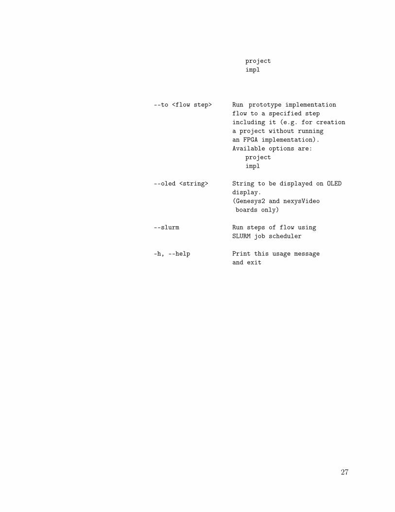
--from <flow step> Start prototype implementationflow from a particular step(e.g. when for generating anewbitfile w/o creating aproject).Available options are:
26
projectimpl
--to <flow step> Run prototype implementationflow to a specified stepincluding it (e.g. for creationa project without runningan FPGA implementation).Available options are:
projectimpl
--oled <string> String to be displayed on OLEDdisplay.(Genesys2 and nexysVideoboards only)
--slurm Run steps of flow usingSLURM job scheduler
-h, --help Print this usage messageand exit
27

B pitonstream manpage
pitonstream -b <board type> -s <storage type> -f<filename> [options]
Required Options:-b, --board <board type> Name of a supported
Xilinx’s developmentboard. Available options:
vc707genesys2nexysVideo
-f, --file <filename> File name withtest names. If option--ustr is not specified,they should be assemblytest names, otherwiselist of generated.ustr files
-p <portname> Port name for serialdevice of FPGA boardon a host PC.Default:
ttyUSB0
--ustr Specifies that test namesin the file should betreated as .ustr filenames
-h, --help Display this help messageand exit
Note: port name can be checked in /dev on Linux. Simplyunplug and plug again a cable connecting a board, and checkwhich device appears when you plug back.
28
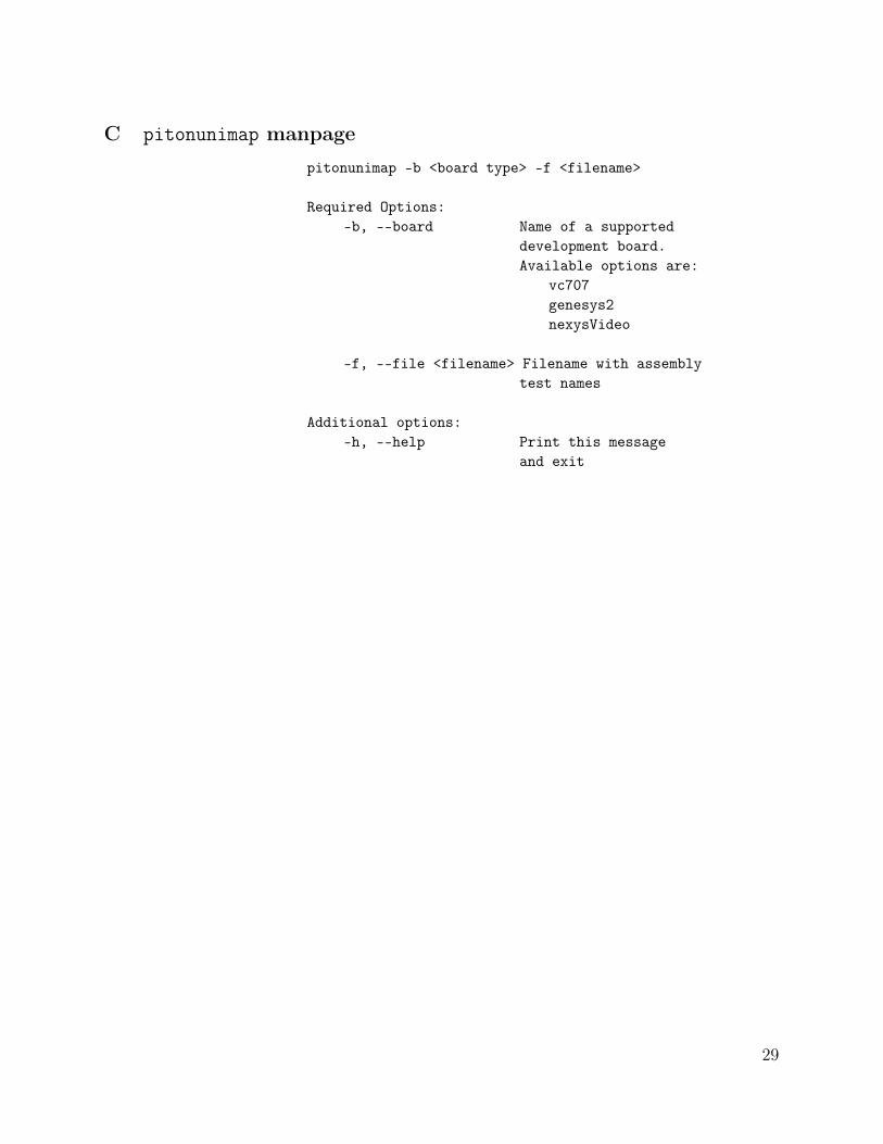
C pitonunimap manpage
pitonunimap -b <board type> -f <filename>
Required Options:-b, --board Name of a supported
development board.Available options are:
vc707genesys2nexysVideo
-f, --file <filename> Filename with assemblytest names
Additional options:-h, --help Print this message
and exit
29

D .ustr file format
.ustr file starts with40’haaaaaaaaaa- initial synchronization sequence for FPGA FSM.
After that there are N groups, each consisting of the next fields:40’h - memory start address for data4’h - number of sequential data blocks in a group128’h x specified number of blocks - data blocks, 512-bits each,stored from MSB on the left to LSB on the right. Address ofthe next block increases from previous one by 8’h40
Group with address 40’hffffffffff, 8’h00 number of blocksand 8’h00 data block serves as a stop sequence for UART stream.
30

E Porting OpenPiton Prototype to a Custom Development Board
FPGA project can be ported to development boards differentfrom supported ones. Follow the steps below to create a newproject and configure it for OpenPiton prototype. Instruc-tions are presented based on Xilinx Vivado 2015.4 tool, butthey also can be used as a guideline for other versions or tools.Project for Genesys2 development board with respective scriptsin $DV_ROOT/tools/src/proto/genesys2 can be taken as a ref-erence.
1. Create a new folder in $DV_ROOT/tools/src/proto direc-tory (e.g. new_board)
2. Create a new folder with the same name as above in$MODEL_DIR directory
3. Open your tool and choose "Create New Project"
4. Set up new project name and its location (e.g. createa project with the name of your development board andchoose $MODEL_DIR/<new_board location)
5. Choose RTL Project Type
6. Add source files to the project*
*Vivado 2015.4: this step can be skipped and scriptadd_files.tcl can be run instead from Vivado’s Tcl Con-sole (see below)
7. Add IP necessary cores*
*Vivado 2015.4: folder$DV_ROOT/tools/src/proto/genesys2/ip_cores canbe copied to $MODEL_DIR/new_folder and added as adirectory to the project
8. Add a constraint file to your design*. File$DV_ROOT/tools/src/proto/genesys2/constraints.xdccan be taken as a reference. Note that pin names andclock constraints will require changes to match you FPGApin-out.
*Vivado 2015.4: copy$PITON_ROOT/tools/src/proto/genesys2/constraints.xdcto $MODEL_DIR/new_folder and add it to the project
9. Select a targeted FPGA or development board type
31

10. Finish project creation
11. Vivado 2015.4: copy all .coe files from$DV_ROOT/tools/src/proto/common to a recentlycreated $MODEL_DIR/new_folder
12. Vivado 2015.4: copy $PITON_ROOT/tools/src/proto/add_files.tclto $MODEL_DIR/new_folder, go to that directory inTcl Console and execute source add_files.tcl. Thiscommand will add necessary source files, set the top levelfile, add a constraint file and set defines.
13. Vivado 2015.4: if you are receiving warnings aboutlocked IPs, try to run upgrade ip [get ips -all] fromits Tcl Console. If it doesn’t remove all warnings, youwill have to regenerate those IP cores manually.
Note: mig_7series_0 IP core will not be updated cor-rectly in any case because of pin constraints. See the stepbelow on a required procedure to generate it for Vivado2015.4
14. Vivado 2015.4: Regenerate MIG with settings recom-mended for your FPGA. Due to design constraints it is rec-ommended to choose 4:1 PHY to Controller ClockRatio, System Clock - “No Buffer” , ReferenceClock - “Use System Clock” , and enable XADC in-stantiation.
15. Vivado 2015.4: Update Write and Read width foruart_mig_afifo IP core, which depends on MIG settingsand must be equal to ‘MIG APP ADDR WIDTH+‘MIG APPDATA WIDTH+‘MIG APP MASK WIDTH
16. Vivado 2015.4: Set up necessary type of clock inputfor clk_mmcm IP (single ended VS differential). Seta targeted clock frequency and update uart_16550,afifo_mem_splitter, afifo_splitter_mem, anduart_mig_afifo IP cores to match the frequency ofa generated clock.
17. Modify the next files to specify clock type, reset level, andDDR interface of your board.
• $DV_ROOT/design/proto/fpga_top.v
– Add additional preprocessor directive if you have
32

differential clock and/or high active reset level
• $DV_ROOT/verif/env/manycore/manycore_top.v.xlx.v
– Add additional preprocessor directives if you havedifferential clock and/or high active reset level
– if DDR is planned to use, create wires with re-spective interface width under a new define formodule interface in instance of mc_top module
• $DV_ROOT/design/fpga/include/mc_define.h
– set width of DDR data bus - DDR3 DQ WIDTH*
*Vivado 2015.4: set parameters of MIG as theyare in generated IP core
• $DV_ROOT/design/fpga/mc/rtl/mc_top.v
– if DDR is planned to use, create wires with re-spective interface width under the same define asabove
18. Set defines required for you configuration*
*For Vivado 2015.4: If you ran add_files.tcl script, itadded the following defines to your project:NO_SCANFPGA_SYNFPGA_SYN_1THREAD FPGA_SYNPITON_PROTONO_USE_IBM_SRAMSPITON_FPGA_NO_DMBRPITON_FPGA_MC_DDR3PITON_FPGA_SD_BOOTCheck define description in Section 5.1
19. Set a top level source file to cmp_top.v*
*Vivado 2015.4: If you ran source add_files.tcl, itis already done for you
20. If you are planning to run OBP from BRAM, make surethat the frequency of a reference clock for UART in Hyper-Visor matches the system clock in the design. If necessary,regenerate obp.coe file and bram_16384x512 IP core.
33

After these steps steps you should be able to run implementationof OpenPiton for your FPGA.
34

F Step-by-Step Instructions for Booting Debian Linux andPlaying Tetris
Below are steps required to build an OpenPiton prototype tar-geting Digilent Genesys2 development board and run Tetris ona full stack Debian Linux:
• download tar.gz archive of OpenPiton release
• extract it and set up your environment and tools (see Sec-tion 1.2)
• run protosyn -b genesys2 and wait until script exists
• because Vivado creates separate processes for itstasks, protosyn exits before Vivado generatesa .bit file. You need to check runme.log in$MODEL_DIR/genesys2/genesys2_piton/genesys2_piton.runs/impl_1to make ensure that bit file was successfully generated.
• open Hardware Manager in Vivado or Vivado Lab Edi-tion connected to Genesys2 board
• open a target and program the board with a generated.bit file
• put image file with OpenBoot and OS image onto SD card
• insert the SD card into the board and press RESET button
• wait for Open Boot to start OK boot prompt
• print boot Linux command in OK boot prompt
• wait for Linux to boot
• use root both as login and password
• print tetris in Linux prompt and play the game!
35

Figure 5: Genesys2 board running Tetris on full stack DebianLinux
36

G Generating an SD-Bootable Image
We consider this guide to be deprecated as we provideworking disk images. Please check our download pagefor the most up-to-date images. If you wish to buildan image of your own, you will want to adapt the in-structions to fit a newer Debian release (one targetingSPARC64).
This appendix explains in detail how to generate an SD-bootableimage of Debian for SPARC (not SPARC64) for OpenPiton onan FPGA. Each image consists of two items:
• An existing PROM file that contains a copy of the hyper-visor and OpenBoot. This binary is tuned to your FPGA’sprimary clock frequency and RAM size.
• A ramdisk, which contains SILO, a bootable version ofLinux, and a full filesystem.
The PROM files are pre-generated, but you can create and mod-ify your own ramdisk to customize the software you want to runon OpenPiton. Ramdisks can be generated from scratch, but werecommend that you use our distribution as a starting point.
G.1 Building a Ramdisk from Scratch
In order to create a ramdisk from scratch, simply follow thesesteps on a machine running Linux.
G.1.1 Initialization
First, create an empty ramdisk. Simply execute the following in-struction, replacing {size} with the desired size of your ramdiskin megabytes (be sure to add the extra 16 in the command belowas noted - this space is for the PROM).
dd if=/dev/zero of=ramdisk bs=1M count={size + 16}
Next, create a Sun disk partition in this file. Run parted andenter the following commands in order to navigate its menus.Note that if /dev/loop0 is already in use, you can change the 0to another number. losetup -a will show the status of all loopdevices.
sudo losetup -o 16777216 /dev/loop0 ramdisksudo parted /dev/loop0
37
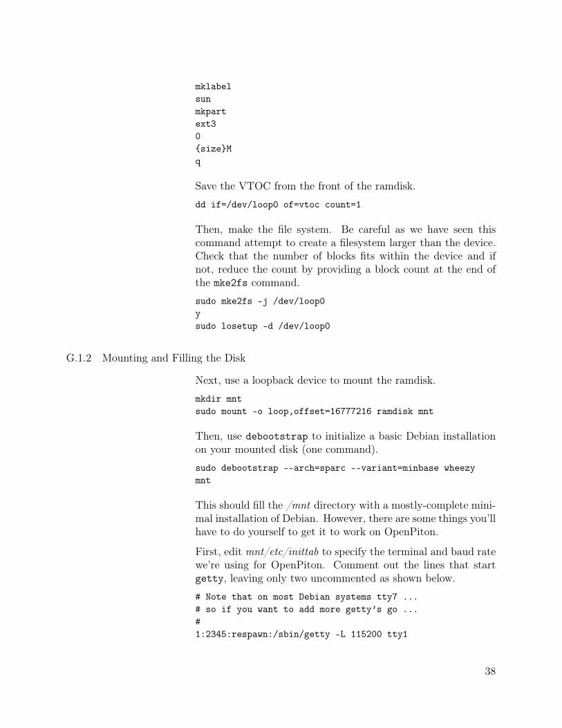
mklabelsunmkpartext30{size}Mq
Save the VTOC from the front of the ramdisk.
dd if=/dev/loop0 of=vtoc count=1
Then, make the file system. Be careful as we have seen thiscommand attempt to create a filesystem larger than the device.Check that the number of blocks fits within the device and ifnot, reduce the count by providing a block count at the end ofthe mke2fs command.
sudo mke2fs -j /dev/loop0ysudo losetup -d /dev/loop0
G.1.2 Mounting and Filling the Disk
Next, use a loopback device to mount the ramdisk.
mkdir mntsudo mount -o loop,offset=16777216 ramdisk mnt
Then, use debootstrap to initialize a basic Debian installationon your mounted disk (one command).
sudo debootstrap --arch=sparc --variant=minbase wheezymnt
This should fill the /mnt directory with a mostly-complete mini-mal installation of Debian. However, there are some things you’llhave to do yourself to get it to work on OpenPiton.
First, edit mnt/etc/inittab to specify the terminal and baud ratewe’re using for OpenPiton. Comment out the lines that startgetty, leaving only two uncommented as shown below.
# Note that on most Debian systems tty7 ...# so if you want to add more getty’s go ...#1:2345:respawn:/sbin/getty -L 115200 tty1
38

#1:2345:respawn:/bin/login ttyS0 </dev/ttyS0 >/dev/ttyS02>&1#2:23:respawn:/sbin/getty 38400 tty2#3:23:respawn:/sbin/getty 38400 tty3#4:23:respawn:/sbin/getty 38400 tty4#5:23:respawn:/sbin/getty 38400 tty5#6:23:respawn:/sbin/getty 38400 tty6
# Example how to put a getty on a serial line (for aterminal)##s0:2345:respawn:/sbin/agetty -L --noclear ttyS0 115200vt100T0:2345:respawn:/sbin/getty -L ttyS0 115200 vt100#T1:23:respawn:/sbin/getty -L ttyS1 9600 vt100
Then, edit mnt/etc/fstab to enable use of the Sun ramdisk. Re-place the contents of that file with those shown below.
# /etc/fstab: static file system information.
proc /proc proc defaults 0 0/dev/sunhv_disk / ext3defaults,errors=remount-ro,noatime 0 1
Finally, add a symlink to /proc/mounts in the /etc directory.
cd mnt/etcsudo ln -nsf /proc/mounts mtab
Next, we’re going to copy over a valid boot directory. Start withthe boot directory from our provided ramdisk:
cd mntsudo cp path/to/existing/boot/* ./boot
Create symlinks in the root directory to point to silo.conf andvmlinuz.
sudo ln -nsf /boot/vmlinuz vmlinuzsudo ln -nsf /boot/silo.conf silo.confsudo ln -nsf /boot/silo.conf /etc/silo.conf
If you wish to modify the version of Linux being used on theramdisk, please note that you will need to add support for thesunhv disk and network drivers.
39

Finally, we’re going to patch up the silo files. Change directo-ries into the directory containing mnt. Then, run the followingcommand.sudo /sbin/silo -r ./mnt -f -p 0syncsudo umount mntdd if=vtoc of=ramdisk seek=16 conv=notrunc count=1
Your ramdisk file is now ready to be used.
G.2 Modifying an Existing Ramdisk
Once you have a ramdisk (either one you generated or our sup-plied one), you can add or remove files from it on any Linuxmachine. First, mount the ramdisk file to a loopback device:mkdir mntsudo mount -o loop,offset=16777216 ramdisk mnt
Copy any files you want to use into the ramdisk’s filesystem,which is now exposed in the mnt/ directory.
If you want to run apt-get to install new packages, you firstmust chroot into the mnt/ directory.cd mntsudo mount -o bind /proc ./procsudo mount -o bind /dev ./devsudo mount -o bind /sys ./syssudo chroot .
Run apt-get to install any desired packages, making sure to runapt-get clean once you’re finished to clear out the packagemanager’s cache.
To exit, undo your chroot.exitsudo umount ./procsudo umount ./devsudo umount ./sys
To save the modified ramdisk back into the original file, simplyunmount it.cd ..syncsudo umount ./mnt
40

G.3 Creating an SD Image
With a PROM file and a ramdisk ready, simply use dd to writeit to an SD card.
Note: As of the current release, only plain SD cards will workproperly – any SDHC or SDXC cards will not work with Open-Piton’s FPGA implementation.
41

References
[1] D. L. Weaver, “Opensparc internals,” pp. 107–108, Sun Mi-crosystems, Inc., October 2008.
[2] J. Balkind, M. McKeown, Y. Fu, T. Nguyen, Y. Zhou,A. Lavrov, M. Shahrad, A. Fuchs, S. Payne, X. Liang,M. Matl, and D. Wentzlaff, “Openpiton: An open sourcemanycore research framework,” in Proceedings of the TwentyFirst International Conference on Architectural Support forProgramming Languages and Operating Systems, ASPLOS’16, (New York, NY, USA), ACM, 2016.
[3] X. Inc., “Vc707 evaluation board for the virtex-7 fpga userguide,” April 7, 2015.
[4] X. Inc., “7 series fpgas memory interface solutions,” March 1,2011.
[5] Y. Zhou and D. Wentzlaff, “Mitts: Memory inter-arrival timetraffic shaping,” in Proceedings of the 43rd International Sym-posium on Computer Architecture, ISCA ’16, (New York, NY,USA), ACM, 2016.
[6] X. Inc., “Vivado design suite user guide,” June 24, 2015.
42
Related Documents