ADC C VREF VSS VDD 5 V 3.3 V R OPAx325 Input + –150 –125 –100 –75 –50 –25 0 25 50 75 100 125 150 –3 –2 –1 0 1 2 3 V OS (V) V CM (V) C003 V CM = –2.85 V V CM = 2.85 V Product Folder Order Now Technical Documents Tools & Software Support & Community Reference Design An IMPORTANT NOTICE at the end of this data sheet addresses availability, warranty, changes, use in safety-critical applications, intellectual property matters and other important disclaimers. PRODUCTION DATA. OPA325, OPA2325, OPA4325 SBOS637D – OCTOBER 2016 – REVISED JUNE 2019 OPAx325 Precision, 10-MHz, Low-Noise, Low-Power, RRIO, CMOS Operational Amplifiers 1 1 Features 1• Precision with zero-crossover distortion: – Low offset voltage: 150 μV (maximum) – High CMRR: 114 dB – Rail-to-rail I/O • Wide bandwidth: 10 MHz • Quiescent current: 650 μA/ch • Single-supply voltage range: 2.2 V to 5.5 V • Low input bias current: 0.2 pA • Low noise: 9 nV/√Hz at 10 kHz • Slew rate: 5 V/μs • Unity-gain stable 2 Applications • High-Z sensor signal conditioning • Transimpedance amplifiers • Test and measurement equipment • Programmable logic controllers (PLCs) • Motor control loops • Communications • Input, output ADC, and DAC buffers • Active filters Offset Voltage vs Input Common-Mode Voltage 3 Description The OPA325, OPA2325, and OPA4325 (OPAx325) are precision, low-voltage complementary metal-oxide semiconductor (CMOS) operational amplifiers optimized for very low noise and wide bandwidth, while operating on a low quiescent current of only 650 μA. The OPAx325 feature a linear input stage with zero- crossover distortion that delivers excellent common- mode rejection ratio (CMRR) of typically 114 dB over the entire input range. The input common-mode range extends 100 mV beyond the negative and positive supply rails. The output voltage typically swings within 10 mV of the rails. The zero-crossover distortion, combined with wide bandwidth (10 MHz), high slew rate (5 V/μs), and low noise (9 nV/√Hz), make the OPAx325 a very good successive-approximation register (SAR) analog-to- digital converter (ADC) input driver amplifier. In addition, the OPAx325 have a wide supply-voltage range from 2.2 V to 5.5 V, with excellent power- supply rejection ratio (PSRR) over the entire supply range, making the device an excellent choice for precision, low-power applications that run directly from batteries without regulation. The OPA325 (single-channel version) is available in the SOT23-5 package. The OPA2325 (dual-channel version) is offered in SO-8 and MSOP-8 packages. The OPA4325 (quad-channel version) is available in TSSOP-14 package. Device Information (1) PART NUMBER PACKAGE BODY SIZE (NOM) OPA325 SOT-23 (5) 2.90 mm × 1.60 mm OPA2325 SOIC (8) 4.90 mm × 3.91 mm VSSOP (8) 3.00 mm × 3.00 mm OPA4325 TSSOP (14) 5.00 mm × 4.40 mm (1) For all available packages, see the package option addendum at the end of the data sheet. The OPAx325 as an ADC Driver Amplifier

Welcome message from author
This document is posted to help you gain knowledge. Please leave a comment to let me know what you think about it! Share it to your friends and learn new things together.
Transcript

ADC
C
VREF
VSS VDD
5 V
3.3 V
R
OPAx325
Input +
±150
±125
±100
±75
±50
±25
0
25
50
75
100
125
150
±3 ±2 ±1 0 1 2 3
VO
S (�
V)
VCM (V) C003
VCM = ±2.85 V VCM = 2.85 V
Product
Folder
Order
Now
Technical
Documents
Tools &
Software
Support &Community
ReferenceDesign
An IMPORTANT NOTICE at the end of this data sheet addresses availability, warranty, changes, use in safety-critical applications,intellectual property matters and other important disclaimers. PRODUCTION DATA.
OPA325, OPA2325, OPA4325SBOS637D –OCTOBER 2016–REVISED JUNE 2019
OPAx325Precision, 10-MHz, Low-Noise, Low-Power, RRIO, CMOS Operational Amplifiers
1
1 Features1• Precision with zero-crossover distortion:
– Low offset voltage: 150 μV (maximum)– High CMRR: 114 dB– Rail-to-rail I/O
• Wide bandwidth: 10 MHz• Quiescent current: 650 μA/ch• Single-supply voltage range: 2.2 V to 5.5 V• Low input bias current: 0.2 pA• Low noise: 9 nV/√Hz at 10 kHz• Slew rate: 5 V/μs• Unity-gain stable
2 Applications• High-Z sensor signal conditioning• Transimpedance amplifiers• Test and measurement equipment• Programmable logic controllers (PLCs)• Motor control loops• Communications• Input, output ADC, and DAC buffers• Active filters
Offset Voltage vs Input Common-Mode Voltage
3 DescriptionThe OPA325, OPA2325, and OPA4325 (OPAx325)are precision, low-voltage complementary metal-oxidesemiconductor (CMOS) operational amplifiersoptimized for very low noise and wide bandwidth,while operating on a low quiescent current of only650 μA.
The OPAx325 feature a linear input stage with zero-crossover distortion that delivers excellent common-mode rejection ratio (CMRR) of typically 114 dB overthe entire input range. The input common-moderange extends 100 mV beyond the negative andpositive supply rails. The output voltage typicallyswings within 10 mV of the rails.
The zero-crossover distortion, combined with widebandwidth (10 MHz), high slew rate (5 V/µs), and lownoise (9 nV/√Hz), make the OPAx325 a very goodsuccessive-approximation register (SAR) analog-to-digital converter (ADC) input driver amplifier. Inaddition, the OPAx325 have a wide supply-voltagerange from 2.2 V to 5.5 V, with excellent power-supply rejection ratio (PSRR) over the entire supplyrange, making the device an excellent choice forprecision, low-power applications that run directlyfrom batteries without regulation.
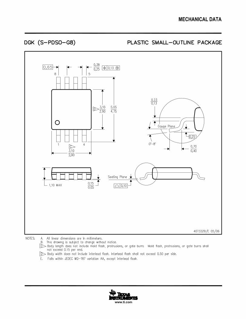
The OPA325 (single-channel version) is available inthe SOT23-5 package. The OPA2325 (dual-channelversion) is offered in SO-8 and MSOP-8 packages.The OPA4325 (quad-channel version) is available inTSSOP-14 package.
Device Information(1)
PART NUMBER PACKAGE BODY SIZE (NOM)OPA325 SOT-23 (5) 2.90 mm × 1.60 mm
OPA2325SOIC (8) 4.90 mm × 3.91 mmVSSOP (8) 3.00 mm × 3.00 mm
OPA4325 TSSOP (14) 5.00 mm × 4.40 mm
(1) For all available packages, see the package option addendumat the end of the data sheet.
The OPAx325 as an ADC Driver Amplifier
2
OPA325, OPA2325, OPA4325SBOS637D –OCTOBER 2016–REVISED JUNE 2019 www.ti.com
Product Folder Links: OPA325 OPA2325 OPA4325
Submit Documentation Feedback Copyright © 2016–2019, Texas Instruments Incorporated
Table of Contents1 Features .................................................................. 12 Applications ........................................................... 13 Description ............................................................. 14 Revision History..................................................... 25 Pin Configuration and Functions ......................... 36 Specifications......................................................... 5
6.1 Absolute Maximum Ratings ...................................... 56.2 ESD Ratings.............................................................. 56.3 Recommended Operating Conditions....................... 56.4 Thermal Information: OPA325 .................................. 66.5 Thermal Information: OPA2325 ................................ 66.6 Thermal Information: OPA4325 ................................ 66.7 Electrical Characteristics: VS = 2.2 V to 5.5 V or
±1.1 V to ±2.75 V ....................................................... 76.8 Typical Characteristics .............................................. 9
7 Detailed Description ............................................ 167.1 Overview ................................................................. 167.2 Functional Block Diagram ....................................... 167.3 Feature Description................................................. 17
7.4 Device Functional Modes........................................ 188 Application and Implementation ........................ 19
8.1 Application Information............................................ 198.2 Typical Application .................................................. 20
9 Power Supply Recommendations ...................... 2510 Layout................................................................... 25
10.1 Layout Guidelines ................................................. 2510.2 Layout Example .................................................... 26
11 Device and Documentation Support ................. 2711.1 Documentation Support ........................................ 2711.2 Related Links ........................................................ 2711.3 Receiving Notification of Documentation Updates 2711.4 Community Resources.......................................... 2711.5 Trademarks ........................................................... 2711.6 Electrostatic Discharge Caution............................ 2711.7 Glossary ................................................................ 27
12 Mechanical, Packaging, and OrderableInformation ........................................................... 27
4 Revision HistoryNOTE: Page numbers for previous revisions may differ from page numbers in the current version.
Changes from Revision C (May 2019) to Revision D Page
• Added OPA325 and associated content to data sheet .......................................................................................................... 1
Changes from Revision B (February 2019) to Revision C Page
• Changed OPA4325 device status from preview to production data (active) ......................................................................... 1
Changes from Revision A (July 2017) to Revision B Page
• Added OPA4325 advance information device to data sheet.................................................................................................. 1• Added operating temperature to Absolute Maximum Ratings table ....................................................................................... 5• Deleted specified temperature from Absolute Maximum Ratings table; specified temperature already listed in
Recommended Operating Conditions table............................................................................................................................ 5
Changes from Original (October 2016) to Revision A Page
• Added new VSSOP package option for dual-channel device ................................................................................................ 1• Added top navigator icon for TI reference design ................................................................................................................. 1

1OUT A 8 V+
2±IN A 7 OUT B
3+IN A 6 ±IN B
4V± 5 +IN B
Not to scale
+ ±
1OUT
2V±
3+IN 4 ±IN
5 V+
Not to scale
3
OPA325, OPA2325, OPA4325www.ti.com SBOS637D –OCTOBER 2016–REVISED JUNE 2019
Product Folder Links: OPA325 OPA2325 OPA4325
Submit Documentation FeedbackCopyright © 2016–2019, Texas Instruments Incorporated
5 Pin Configuration and Functions
OPA325: DBV Package5-Pin SOT-23
Top View
Pin Functions: OPA325PIN
I/O DESCRIPTIONNAME NO.–IN 4 I Inverting input+IN 3 I Noninverting inputOUT 1 O OutputV– 2 — Negative (lowest) power supplyV+ 5 — Positive (highest) power supply
OPA2325: D and DGK Packages8-Pin SOIC, 8-Pin VSSOP
Top View
Pin Functions: OPA2325PIN
I/O DESCRIPTIONNAME NO.–IN A 2 I Inverting input channel A+IN A 3 I Noninverting input channel A–IN B 6 I Inverting input channel B+IN B 5 I Noninverting input channel BOUT A 1 O Output channel AOUT B 7 O Output channel BV– 4 — Negative supplyV+ 8 — Positive supply

1OUT A 14 OUT D
2±IN A 13 ±IN D
3+IN A 12 +IN D
4V+ 11 V±
5+IN B 10 +IN C
6±IN B 9 ±IN C
7OUT B 8 OUT C
Not to scale
4
OPA325, OPA2325, OPA4325SBOS637D –OCTOBER 2016–REVISED JUNE 2019 www.ti.com
Product Folder Links: OPA325 OPA2325 OPA4325
Submit Documentation Feedback Copyright © 2016–2019, Texas Instruments Incorporated
OPA4325: PW Package14-Pin TSSOP
Top View
Pin Functions: OPA4325PIN
I/O DESCRIPTIONNAME NO.
–IN A 2 I Inverting input channel A+IN A 3 I Noninverting input channel A–IN B 6 I Inverting input channel B+IN B 5 I Noninverting input channel B–IN C 9 I Inverting input channel C+IN C 10 I Noninverting input channel C–IN D 13 I Inverting input channel D+IN D 12 I Noninverting input channel DOUT A 1 O Output channel AOUT B 7 O Output channel BOUT C 8 O Output channel COUT D 14 O Output channel DV– 11 — Negative supplyV+ 4 — Positive supply

5
OPA325, OPA2325, OPA4325www.ti.com SBOS637D –OCTOBER 2016–REVISED JUNE 2019
Product Folder Links: OPA325 OPA2325 OPA4325
Submit Documentation FeedbackCopyright © 2016–2019, Texas Instruments Incorporated
(1) Stresses beyond those listed under Absolute Maximum Ratings may cause permanent damage to the device. These are stress ratingsonly, which do not imply functional operation of the device at these or any other conditions beyond those indicated under RecommendedOperating Conditions. Exposure to absolute-maximum-rated conditions for extended periods may affect device reliability.
(2) Input pins are diode-clamped to the power-supply rails. Input signals that can swing more than 0.5 V beyond the supply rails must becurrent limited to 10 mA or less.
(3) Short-circuit to ground, one amplifier per package.
6 Specifications
6.1 Absolute Maximum Ratingsover operating free-air temperature range (unless otherwise noted) (1)
MIN MAX UNITSupply voltage VS = (V+) – (V–) 6 V
Signal input pinsVoltage (2) (V–) – 0.5 (V+) + 0.5 VCurrent (2) –10 10 mA
Output short-circuit (3) Continuous mA
TemperatureOperating, TA –40 150
°CJunction, TJ 150Storage, Tstg –65 150
(1) JEDEC document JEP155 states that 500-V HBM allows safe manufacturing with a standard ESD control process.(2) JEDEC document JEP157 states that 250-V CDM allows safe manufacturing with a standard ESD control process.
6.2 ESD RatingsVALUE UNIT
V(ESD) Electrostatic dischargeHuman-body model (HBM), per ANSI/ESDA/JEDEC JS-001 (1) ±4000
VCharged-device model (CDM), per JEDEC specification JESD22-C101 (2) ±1000
6.3 Recommended Operating Conditionsover operating free-air temperature range (unless otherwise noted)
MIN NOM MAX UNIT
VS Supply voltageSingle supply 2.2 5.5
VDual supply ±1.1 ±2.75
TA Specified temperature –40 125 °C

6
OPA325, OPA2325, OPA4325SBOS637D –OCTOBER 2016–REVISED JUNE 2019 www.ti.com
Product Folder Links: OPA325 OPA2325 OPA4325
Submit Documentation Feedback Copyright © 2016–2019, Texas Instruments Incorporated
(1) For more information about traditional and new thermal metrics, see the Semiconductor and IC Package Thermal Metrics applicationreport.
6.4 Thermal Information: OPA325
THERMAL METRIC (1)OPA325
UNITDBV (SOT)5 PINS
RθJA Junction-to-ambient thermal resistance 205 °C/WRθJC(top) Junction-to-case (top) thermal resistance 200 °C/WRθJB Junction-to-board thermal resistance 113 °C/WΨJT Junction-to-top characterization parameter 38.2 °C/WΨJB Junction-to-board characterization parameter 104.9 °C/WRθJC(bot) Junction-to-case (bottom) thermal resistance N/A °C/W
(1) For more information about traditional and new thermal metrics, see the Semiconductor and IC Package Thermal Metrics applicationreport.
6.5 Thermal Information: OPA2325
THERMAL METRIC (1)OPA2325
UNITD (SOIC) DGK (VSSOP)8 PINS 8 PINS
RθJA Junction-to-ambient thermal resistance 119 143 °C/WRθJC(top) Junction-to-case (top) thermal resistance 60 47 °C/WRθJB Junction-to-board thermal resistance 61 64 °C/WΨJT Junction-to-top characterization parameter 15.0 5.3 °C/WΨJB Junction-to-board characterization parameter 60.4 62.8 °C/WRθJC(bot) Junction-to-case (bottom) thermal resistance N/A N/A °C/W
(1) For more information about traditional and new thermal metrics, see the Semiconductor and IC Package Thermal Metrics applicationreport.
6.6 Thermal Information: OPA4325
THERMAL METRIC (1)OPA4325
UNITPW (TSSOP)14 PINS
RθJA Junction-to-ambient thermal resistance 93 °C/WRθJC(top) Junction-to-case (top) thermal resistance 28 °C/WRθJB Junction-to-board thermal resistance 34 °C/WΨJT Junction-to-top characterization parameter 1.9 °C/WΨJB Junction-to-board characterization parameter 33.1 °C/WRθJC(bot) Junction-to-case (bottom) thermal resistance N/A °C/W

7
OPA325, OPA2325, OPA4325www.ti.com SBOS637D –OCTOBER 2016–REVISED JUNE 2019
Product Folder Links: OPA325 OPA2325 OPA4325
Submit Documentation FeedbackCopyright © 2016–2019, Texas Instruments Incorporated
(1) Third-order filter; bandwidth = 80 kHz at –3 dB.
6.7 Electrical Characteristics: VS = 2.2 V to 5.5 V or ±1.1 V to ±2.75 Vat TA = 25°C, RL = 10 kΩ connected to VS / 2, VCM = VS / 2, and VOUT = VS / 2 (unless otherwise noted)
PARAMETER TEST CONDITIONS MIN TYP MAX UNIT
OFFSET VOLTAGE
VOS Input offset voltage 40 150 µV
dVOS/dT Input offset voltage drift VS = 5.5 V, TA = –40°C to +125°C 2 7.5 µV/°C
PSRR Power-supply rejection ratioVS = 2.2 V to +5.5 V 6 20
µV/VVS = 2.2 V to 5.5 V, TA = –40°C to +125°C 15
Channel separation At 1 kHz 130 dB
INPUT VOLTAGE
VCM Common-mode voltage range (V–) – 0.1 (V+) + 0.1 V
CMRR Common-mode rejection ratioVS = 5.5 V, (V–) – 0.1 V < VCM < (V+) + 0.1 V 100 114
dBTA = –40°C to +125°C 95
INPUT BIAS CURRENT
IB Input bias current
±0.2 ±10pA
TA = –40°C to +85°C ±500
TA = –40°C to +125°C ±10 nA
IOS Input offset current
±0.2 ±10pA
TA = –40°C to +85°C ±500
TA = –40°C to +125°C ±10 nA
NOISE
Input voltage noise f = 0.1 Hz to 10 Hz 2.8 µVPP
en Input voltage noise densityf = 1 kHz 10
nV/√Hzf = 10 kHz 9
in Input current noise density f = 1 kHz 1.3 fA/√Hz
INPUT CAPACITANCE
Differential 5 pF
Common-mode 4 pF
OPEN-LOOP GAIN
AOL Open-loop voltage gain
0.1 V < VO < (V+) – 0.1 V, RL = 10 kΩ 105 130
dB0.1 V < VO < (V+) – 0.1 V, RL = 10 kΩ,TA = –40°C to +125°C 95 128
0.2 V < VO < (V+) – 0.2 V, RL = 2 kΩ 100 110
PM Phase margin G = 1 V/V, VS = 5 V, CL = 15 pF 67 Degrees
FREQUENCY RESPONSE (VS = 5.0 V, CL = 50 pF)
GBP Gain bandwidth product Unity gain 10 MHz
SR Slew rate G = +1 5 V/μs
tS Settling timeTo 0.1%, 2-V step, G = +1 0.6
µsTo 0.01%, 2-V step, G = +1 1
Overload recovery time VIN × G > VS 200 ns
THD+N Total harmonic distortion + noise (1) VO = 4 VPP, G = +1, f = 10 kHz, RL = 10 kΩ 0.0005%
VO = 2 VPP, G = +1, f = 10 kHz, RL = 600 Ω 0.005%

8
OPA325, OPA2325, OPA4325SBOS637D –OCTOBER 2016–REVISED JUNE 2019 www.ti.com
Product Folder Links: OPA325 OPA2325 OPA4325
Submit Documentation Feedback Copyright © 2016–2019, Texas Instruments Incorporated
Electrical Characteristics: VS = 2.2 V to 5.5 V or ±1.1 V to ±2.75 V (continued)at TA = 25°C, RL = 10 kΩ connected to VS / 2, VCM = VS / 2, and VOUT = VS / 2 (unless otherwise noted)
PARAMETER TEST CONDITIONS MIN TYP MAX UNIT
OUTPUT
VO Voltage output swing from both rails
RL = 10 kΩ 10 20
mVRL = 10 kΩ, TA = –40°C to +125°C 30
RL = 2 kΩ 25 45
RL = 2 kΩ, TA = –40°C to +125°C 55
ISC Short-circuit current VS = 5.5 V See the Typical Characteristics mA
CL Capacitive load drive See the Typical Characteristics
RO Open-loop output resistance IO = 0 mA, f = 1 MHz 180 Ω
POWER SUPPLY
IQ Quiescent current per amplifierIO = 0 mA, VS = 5.5 V 0.65 0.75
mAIO = 0 mA, VS = 5.5 V, TA = –40°C to +125°C 0.8
Power-on time V+ = 0 V to 5 V, to 90% IQ level 28 µs

±150
±100
±50
0
50
100
150
1.0 1.2 1.4 1.6 1.8 2.0 2.2 2.4 2.6 2.8 3.0
VO
S (�
V)
VSUPPLY (V) C017
VS = ± 2.75 V
VS = ± 1.1 V
0
45
90
135
180
±20
0
20
40
60
80
100
120
140
1 10 100 1k 10k 100k 1M 10M
Phase (deg) G
ain
(dB
)
Frequency (Hz) C200
Gain
Phase
±150
±125
±100
±75
±50
±25
0
25
50
75
100
125
150
±3 ±2 ±1 0 1 2 3
VO
S (�
V)
VCM (V) C003
VCM = ±2.85 V VCM = 2.85 V
±500
±400
±300
±200
±100
0
100
200
300
400
500
±75 ±50 ±25 0 25 50 75 100 125 150
VO
S (�
V)
Temperature (�C) C010
0
5
10
15
-150
-100 -5
0 0 50 100
150
Am
plifi
ers
(%)
Offset Voltage (µV) C002
0
5
10
15
20
-7.5 -6
-4.5 -3
-1.5 0
1.5 3
4.5 6
7.5
Am
plifi
ers
(%)
Offset Voltage Drift (µV/�C) C001
9
OPA325, OPA2325, OPA4325www.ti.com SBOS637D –OCTOBER 2016–REVISED JUNE 2019
Product Folder Links: OPA325 OPA2325 OPA4325
Submit Documentation FeedbackCopyright © 2016–2019, Texas Instruments Incorporated
6.8 Typical Characteristicsat TA = 25°C, VCM = VOUT = midsupply, and RL = 10 kΩ (unless otherwise noted)
Figure 1. Offset Voltage Production Distribution Histogram Figure 2. Offset Voltage Drift Distribution Histogram
Figure 3. Offset Voltage vs Common-Mode Voltage Figure 4. Offset Voltage vs Temperature
CL = 15 pF
Figure 5. Open-Loop Gain and Phase vs Frequency Figure 6. Offset Voltage vs Supply Voltage

0
5
10
15
20
-2 -1 0 1 2
Am
plifi
ers
(%)
Input Bias Current (pA)
C015
±10
±8
±6
±4
±2
0
2
4
6
8
10
±3 ±2 ±1 0 1 2 3
Inpu
t B
ias
Cur
rent
(pA
)
VCM (V) C013
0
100
200
300
400
500
600
700
800
0 0.5 1 1.5 2 2.5 3
I Q (
µA
)
Supply Voltage (V) C004
0
100
200
300
400
500
600
700
800
900
1000
±75 ±50 ±25 0 25 50 75 100 125 150
I Q (
µA
)
Temperature (�C) C007
VS = ± 2.75 V
VS = ± 1.1 V
±40.0
±30.0
±20.0
±10.0
0.0
10.0
20.0
30.0
40.0
±75 ±50 ±25 0 25 50 75 100 125 150
AO
L (µ
V/V
)
Temperature (�C) C005
VS = ± 2.75 V
VS = ± 1.1 V
±40.0
±30.0
±20.0
±10.0
0.0
10.0
20.0
30.0
40.0
±75 ±50 ±25 0 25 50 75 100 125 150
AO
L (µ
V/V
)
Temperature (�C) C006
VS = ±2.75 V
VS = ±1.1 V
10
OPA325, OPA2325, OPA4325SBOS637D –OCTOBER 2016–REVISED JUNE 2019 www.ti.com
Product Folder Links: OPA325 OPA2325 OPA4325
Submit Documentation Feedback Copyright © 2016–2019, Texas Instruments Incorporated
Typical Characteristics (continued)at TA = 25°C, VCM = VOUT = midsupply, and RL = 10 kΩ (unless otherwise noted)
RL = 10 kΩ
Figure 7. Open-Loop Gain vs Temperature
RL = 2 kΩ
Figure 8. Open-Loop Gain vs Temperature
Figure 9. Quiescent Current vs Temperature Figure 10. Quiescent Current vs Supply Voltage
Figure 11. Input Bias Current vs Common-Mode Voltage Figure 12. Input Bias Current Distribution Histogram

0
10
20
30
40
50
60
±75 ±50 ±25 0 25 50 75 100 125 150
I SC (
mA
)
Temperature (�C) C008
ISC, Source
ISC, Sink
0
20
40
60
80
100
120
1 10 100 1k 10k 100k 1M
Pow
er-S
uppl
y R
ejec
tion
Rat
io (
dB),
C
omm
on-M
ode
Rej
ectio
n R
atio
(dB
)
Frequency (Hz) C203
PSRR+
CMRR PSRR-
0
0.5
1
1.5
2
2.5
3
0 10 20 30 40 50 60
VO (
V)
IO (mA) C009A
±40°C
25°C
125°C
85°C
-3
-2.5
-2
-1.5
-1
-0.5
0
0 10 20 30 40 50 60
VO (
V)
IO (mA) C009B
125°C
25°C
±40°C
85°C
0
5
10
15
20
25-2 -1 0 1 2
Am
plifi
ers
(%)
Input Offset Current (pA)
C016
0.0
0.5
1.0
1.5
2.0
±75 ±50 ±25 0 25 50 75 100 125 150
Inpu
t B
ias
Cur
rent
(nA
)
Temperature (�C) C014
IOS
11
OPA325, OPA2325, OPA4325www.ti.com SBOS637D –OCTOBER 2016–REVISED JUNE 2019
Product Folder Links: OPA325 OPA2325 OPA4325
Submit Documentation FeedbackCopyright © 2016–2019, Texas Instruments Incorporated
Typical Characteristics (continued)at TA = 25°C, VCM = VOUT = midsupply, and RL = 10 kΩ (unless otherwise noted)
Figure 13. Input Offset Current Distribution Histogram Figure 14. Input Bias Current vs Temperature
Figure 15. Output Voltage Swing (Positive) vsOutput Current
Figure 16. Output Voltage Swing (Negative) vsOutput Current
Figure 17. Short-Circuit Current vs Temperature Figure 18. CMRR and PSRR vs Frequency

-20
0
20
40
60
100 1k 10k 100k 1M 10M
Gai
n (d
B)
Frequency (Hz) C201
G = +1
G = +10
G = +100
-20
0
20
40
60
100 1k 10k 100k 1M 10M
Gai
n (d
B)
Frequency (Hz) C202
G = +100
G = +10
G = +1
1
10
100
1k
1 10 100 1k 10k 100k
Vol
tage
Noi
se S
pect
ral D
ensi
ty (
nV/¥
Hz)
Frequency (Hz) C205
Vol
tage
(5
00 n
V/d
iv)
Time (1 s/div)
C204
-20
-15
-10
-5
0
5
10
15
20
±75 ±50 ±25 0 25 50 75 100 125 150
Pow
er-S
uppl
y R
ejec
tion
Rat
io (
µV
/V)
Temperature (�C) C012
-15
-10
-5
0
5
10
15
±75 ±50 ±25 0 25 50 75 100 125 150
Com
mon
-Mod
e R
ejec
tion
Rat
io (
µV
/V)
Temperature (�C) C011
12
OPA325, OPA2325, OPA4325SBOS637D –OCTOBER 2016–REVISED JUNE 2019 www.ti.com
Product Folder Links: OPA325 OPA2325 OPA4325
Submit Documentation Feedback Copyright © 2016–2019, Texas Instruments Incorporated
Typical Characteristics (continued)at TA = 25°C, VCM = VOUT = midsupply, and RL = 10 kΩ (unless otherwise noted)
Figure 19. CMRR vs Temperature Figure 20. PSRR vs Temperature
Figure 21. Input Voltage Noise Spectral Density vsFrequency
Figure 22. 0.1-Hz to 10-Hz Input Voltage Noise
VS = 1.8 V, RL = 10 kΩ, CL = 15 pF
Figure 23. Closed-Loop Gain vs Frequency
VS = 5.5 V, RL = 10 kΩ, CL = 15 pF
Figure 24. Closed-Loop Gain vs Frequency

-120
-100
-80
-60
-40
0.0001
0.001
0.01
0.1
1
10 100 1k 10k 100k
Total H
armonic D
istortion + N
oise (dB) T
otal
Har
mon
ic D
isto
rtio
n +
Noi
se (
%)
Frequency (Hz) C004
G = -1, RL = 600 �
G = +1, RL = 600 �
G = -1, RL = 2 k�
G = -1, RL = 10 k�
G = +1, RL = 2 k�
G = +1, RL = 10 k�
-140
-120
-100
-80
-60
-40
0.0001
0.001
0.01
0.1
1
10 100 1k 10k 100k
Total H
armonic D
istortion + N
oise (dB) T
otal
Har
mon
ic D
isto
rtio
n +
Noi
se (
%)
Frequency (Hz) C206
G = -1, RL = 600 �
G = +1, RL = 600 �
G = -1, RL = 2 k�
G = -1, RL = 10 k�
G = +1, RL = 2 k�
G = +1, RL = 10 k�
0
10
20
30
40
50
60
70
0 200 400 600 800 1000
Ove
rsho
ot (
%)
Capacitive Load (pF) C209
G = 1, VS = 1.8 V
G = 1, VS = 5.5 V
G = 10, VS = 5.5 V
G = 10, VS = 5.5 V
-120
-100
-80
-60
0.0001
0.001
0.01
0.1
0.001 0.01 0.1 1
Total H
armonic D
istortion + N
oise (dB) T
otal
Har
mon
ic D
isto
rtio
n +
Noi
se (
%)
Output Amplitude (VRMS) C208
G = -1, RL = 600 �
G = +1, RL = 600 �
G = -1, RL = 2 k�
G = +1, RL = 10 k� G = +1, RL = 2 k�
G = -1, RL = 10 k�
0
1
2
3
4
5
6
7
100 1k 10k 100k 1M 10M
Out
put
Vol
tage
(V
PP)
Frequency (Hz) C218
VS = ±2.5 V
VS = ±0.9 V
10m 100m 1 10 100 1k 10k 100k 1M 10M 100M 1G 100
1k
10k
Ope
n-Lo
op O
utpu
t Im
peda
nce
Frequency (Hz) C025
13
OPA325, OPA2325, OPA4325www.ti.com SBOS637D –OCTOBER 2016–REVISED JUNE 2019
Product Folder Links: OPA325 OPA2325 OPA4325
Submit Documentation FeedbackCopyright © 2016–2019, Texas Instruments Incorporated
Typical Characteristics (continued)at TA = 25°C, VCM = VOUT = midsupply, and RL = 10 kΩ (unless otherwise noted)
Figure 25. Maximum Output Voltage vs Frequency Figure 26. Open-Loop Output Impedance vs Frequency
Figure 27. Small-Signal Overshoot vs Load Capacitance
f = 10 kHz, VS = ±2.5 V, filter bandwidth = 500 kHz
Figure 28. THD+N vs Amplitude
VIN = 2 VPP, VS = ±2.5 V, filter bandwidth = 500 kHz
Figure 29. THD+N vs Frequency
VIN = 4 VPP, VS = ±2.5 V, filter bandwidth = 500 kHz
Figure 30. THD+N vs Frequency

2.5
mV
/div
Time (2.5 µs/div)
VOUT
VIN
C213
100
µV
/div
Time (1 µs/div)
C217
0.01% Settling = �200 µV
1 V
/div
Time (100 µs/div)
C211
VOUT
VIN
5
5.2
5.4
5.6
5.8
6
2 2.5 3 3.5 4 4.5 5 5.5
Sle
w R
ate
(V/µ
s)
Supply Voltage (V) C219
Slew Rate (Rising)
Slew Rate (Falling)
1.25
V/d
iv
Time (50 ms/div)
C210
VOUT
VIN
5 V
/div
Time (100 µs/div)
C212
VIN
VOUT
14
OPA325, OPA2325, OPA4325SBOS637D –OCTOBER 2016–REVISED JUNE 2019 www.ti.com
Product Folder Links: OPA325 OPA2325 OPA4325
Submit Documentation Feedback Copyright © 2016–2019, Texas Instruments Incorporated
Typical Characteristics (continued)at TA = 25°C, VCM = VOUT = midsupply, and RL = 10 kΩ (unless otherwise noted)
Figure 31. No Phase Reversal Figure 32. Positive Overload Recovery
Figure 33. Negative Overload Recovery
CL = 15 pF
Figure 34. Slew Rate vs Supply Voltage
VIN = 10 mVPP, G = +1, CL = 15 pF
Figure 35. Small-Signal Step Response
VIN = 2-V step
Figure 36. 0.01% Positive Settling Time

1 V
/div
Time (2.5 µs/div)
C214
VIN
VOUT
100
µV
/div
Time (1 µs/div)
C216
0.01% Settling = �200 µV
1 V
/div
Time (2.5 µs/div)
C215
VIN
VOUT
15
OPA325, OPA2325, OPA4325www.ti.com SBOS637D –OCTOBER 2016–REVISED JUNE 2019
Product Folder Links: OPA325 OPA2325 OPA4325
Submit Documentation FeedbackCopyright © 2016–2019, Texas Instruments Incorporated
Typical Characteristics (continued)at TA = 25°C, VCM = VOUT = midsupply, and RL = 10 kΩ (unless otherwise noted)
VIN = 2-V step
Figure 37. 0.01% Negative Settling Time
VIN = 4 VPP, G = +1, CL = 15 pF
Figure 38. Large-Signal Step Response
VIN = 4 VPP, G = –1, CL = 15 pF
Figure 39. Large-Signal Step Response

�
e-WULP�
POR
OUT
V+
V�
�IN
+IN
OPAx325
Charge pump
16
OPA325, OPA2325, OPA4325SBOS637D –OCTOBER 2016–REVISED JUNE 2019 www.ti.com
Product Folder Links: OPA325 OPA2325 OPA4325
Submit Documentation Feedback Copyright © 2016–2019, Texas Instruments Incorporated
7 Detailed Description
7.1 OverviewThe OPA325, OPA2325, and OPA4325 (OPAx325) belong to a new generation of low-noise, e-trim™ operationalamplifiers that provide outstanding dc precision. The OPAx325 also have a highly linear input stage with zero-crossover distortion that delivers excellent CMRR and distortion performance across the full rail-to-rail inputrange. In addition, this device has a wide supply range with excellent PSRR. This feature, combined with lowquiescent current, makes the OPAx325 an excellent choice for applications that are battery-powered withoutregulation.
7.2 Functional Block Diagram

±150
±125
±100
±75
±50
±25
0
25
50
75
100
125
150
±3 ±2 ±1 0 1 2 3
VO
S (�
V)
VCM (V) C003
VCM = ±2.85 V VCM = 2.85 V
Input O
ffset V
oltage (
mV
)
-0.5
3
2
1
0
-1
-2
-3
Input Common-Mode Voltage (V)
6.00 0.5 1.0 1.5 2.0 2.5 3.0 3.5 4.0 4.5 5.0 5.5
+V-V
17
OPA325, OPA2325, OPA4325www.ti.com SBOS637D –OCTOBER 2016–REVISED JUNE 2019
Product Folder Links: OPA325 OPA2325 OPA4325
Submit Documentation FeedbackCopyright © 2016–2019, Texas Instruments Incorporated
7.3 Feature Description
7.3.1 Zero-Crossover Input StageTraditional complementary metal-oxide semiconductor (CMOS) rail-to-rail input amplifiers use a complementaryinput stage: an N-channel input differential pair in parallel with a P-channel differential pair. This configurationresults in sudden change in offset voltage when the input stage transitions from the p-channel metal-oxide-semiconductor field effect transistor (PMOS) to the n-type field effect transistor (NMOS), or vice-versa, as shownin Figure 40. This transition results in significant degradation of CMRR and PSRR performance of the amplifier.
.
Figure 40. Input Common-Mode Voltage vs Input Offset Voltage(Traditional Rail-to-Rail Input CMOS Amplifiers)
The OPAx325 series of amplifiers includes an internal charge pump that powers the amplifier input stage with aninternal supply rail that is higher than the external power supply. The internal supply rail allows a singledifferential pair to operate and to be linear across the entire input common-mode voltage range, thus eliminatingcrossover distortion. Rail-to-rail amplifiers that use this technique to eliminate crossover distortion are calledzero-crossover amplifiers.
The single differential pair combined with the charge pump allows the OPAx325 to provide superior CMRRacross the entire common-mode input range, which extends 100 mV beyond both power-supply rails. Figure 41shows the input offset voltage versus input common-mode voltage plot for the OPAx325. Note that unliketraditional rail-to-rail CMOS amplifiers, there is no transition region for the OPAx325.
Figure 41. Offset Voltage vs Common-Mode Voltage (Zero-Crossover)

IOVERLOAD
10 mA max
5 N��
VIN
VOUT
+5V
Current-limiting resistor required if input voltage exceeds supply rails by
> 0.3V.
Copyright © 2016, Texas Instruments Incorporated
0
5
10
15
-150
-100 -5
0 0 50 100
150
Am
plifi
ers
(%)
Offset Voltage (µV) C002
18
OPA325, OPA2325, OPA4325SBOS637D –OCTOBER 2016–REVISED JUNE 2019 www.ti.com
Product Folder Links: OPA325 OPA2325 OPA4325
Submit Documentation Feedback Copyright © 2016–2019, Texas Instruments Incorporated
Feature Description (continued)7.3.2 Low Input Offset VoltageThe OPAx325 are manufactured using TI's e-trim technology. Each amplifier is trimmed in production, therebyminimizing errors associated with input offset voltage. The e-trim technology is a TI proprietary method oftrimming internal device parameters during either wafer probing or final testing. This process allows theOPAx325 to have an excellent offset specification of 150 µV (maximum). Figure 42 shows the offset voltagedistribution for the OPAx325.
Figure 42. Offset Voltage Distribution
7.3.3 Input and ESD ProtectionThe OPAx325 incorporate internal electrostatic discharge (ESD) protection circuits on all pins. In the case ofinput and output pins, this protection primarily consists of current-steering diodes connected between the inputand power-supply pins. These ESD protection diodes also provide in-circuit, input overdrive protection, as longas the current is limited to 10 mA as stated in the Absolute Maximum Ratings table. Figure 43 shows how aseries input resistor can be added to the driven input to limit the input current. The added resistor contributesthermal noise at the amplifier input; thus, keep the value to a minimum in noise-sensitive applications.
Figure 43. Input Current Protection
7.4 Device Functional ModesThe OPAx325 have a single functional mode and are operational when the power-supply voltage is greater than2.2 V (±1.1 V). The maximum power-supply voltage for the OPAx325 is 5.5 V (±2.75 V).

+
±
OPAx325
+5V
0 �F
R2
10 k R1
1 k
+
±
VCM = 2.5 V
VIN
+
±
OUT
Copyright © 2017, Texas Instruments Incorporated
19
OPA325, OPA2325, OPA4325www.ti.com SBOS637D –OCTOBER 2016–REVISED JUNE 2019
Product Folder Links: OPA325 OPA2325 OPA4325
Submit Documentation FeedbackCopyright © 2016–2019, Texas Instruments Incorporated
8 Application and Implementation
NOTEInformation in the following applications sections is not part of the TI componentspecification, and TI does not warrant its accuracy or completeness. TI’s customers areresponsible for determining suitability of components for their purposes. Customers shouldvalidate and test their design implementation to confirm system functionality.
8.1 Application InformationThe OPAx325 series features e-trim, a proprietary technique in which the offset voltage is adjusted during thefinal steps of manufacturing. As a result, the OPAx325 deliver excellent offset voltage (40 μV, typical).Additionally, the amplifier boasts a fast slew rate, low drift, low noise, and excellent PSRR and AOL. TheOPAx325 also feature a linear input stage with zero-crossover distortion, resulting in excellent CMRR over theentire input range, which extends from 100 mV below the negative rail to 100 mV above the positive rail.
8.1.1 Operating CharacteristicsThe OPAx325 family of amplifiers has parameters that are fully specified from 2.2 V to 5.5 V (±1.1 V to ±2.75 V).Many of the specifications apply from –40°C to +125°C. Parameters that can exhibit significant variance withregard to operating voltage or temperature are presented in the Typical Characteristics section.
8.1.2 Basic Amplifier ConfigurationsThe OPAx325 are unity-gain stable. The devices do not exhibit output phase inversion when the input isoverdriven. A typical single-supply connection is shown in Figure 44. The OPAx325 are configured as a basicinverting amplifier with a gain of –10 V/V. This single-supply connection has an output centered on the common-mode voltage, VCM. For the circuit shown, this voltage is 2.5 V, but can be any value within the common-modeinput voltage range.
Figure 44. Basic Single-Supply Connection

+
±
GND
+2.5 V
-2.5 V
VOUT
4 VPP
Sine Wave
OPAx325
ADC
C
VREF
VSS VDD
5 V
3.3 V
R
OPAx325
Input +
20
OPA325, OPA2325, OPA4325SBOS637D –OCTOBER 2016–REVISED JUNE 2019 www.ti.com
Product Folder Links: OPA325 OPA2325 OPA4325
Submit Documentation Feedback Copyright © 2016–2019, Texas Instruments Incorporated
Application Information (continued)8.1.3 Driving an Analog-to-Digital ConverterThe low-noise and wide-gain bandwidth of the OPAx325, combined with rail-to-rail input/output and zero-crossover distortion, make these devices an excellent input driver for ADCs. Figure 45 shows the OPAx325driving an ADC. The amplifier is connected as a unity-gain, noninverting buffer.
Figure 45. The OPAx325 as an Input Driver for ADCs
8.2 Typical ApplicationOperational amplifiers are commonly used as unity-gain buffers. Figure 46 shows the schematic for an amplifierconfigured as a unity-gain buffer. If the input signal range to the amplifier is very close to the rails or includes therails, a rail-to-rail amplifier must be used. However, regular rail-to-rail amplifiers introduce significant distortion tothe signal. This design compares the distortion introduced by a typical CMOS input amplifier with that of theOPAx325 (a zero-crossover amplifier).
Figure 46. The OPAx325 Configured as a Unity-Gain Buffer Amplifier
8.2.1 Design RequirementsThe following parameters are used for this design example:• Gain = +1 V/V (inverting gain)• V+ = 2.5 V, V– = –2.5 V• Input signal = 4 VPP, f = 1-kHz sine wave

NCH3
PCH2
PCH1
IS1
NCH4
+Vsupply
VIN+
VIN±
e-WULP�
±Vsupply
21
OPA325, OPA2325, OPA4325www.ti.com SBOS637D –OCTOBER 2016–REVISED JUNE 2019
Product Folder Links: OPA325 OPA2325 OPA4325
Submit Documentation FeedbackCopyright © 2016–2019, Texas Instruments Incorporated
Typical Application (continued)8.2.2 Detailed Design ProcedureTraditional CMOS rail-to-rail input amplifiers use a complementary input stage: an N-channel input differentialpair in parallel with a P-channel differential pair, as shown in Figure 47.
Figure 47. Complementary Input Stage (Traditional Rail-to-Rail Input CMOS Amplifiers)
PCH2PCH1
IS1
VIN+ VIN±
e-trimTM
Charge Pump
+VSUPPLY
±Vsupply
Input O
ffset V
oltage (
mV
)
-0.5
3
2
1
0
-1
-2
-3
Input Common-Mode Voltage (V)
6.00 0.5 1.0 1.5 2.0 2.5 3.0 3.5 4.0 4.5 5.0 5.5
+V-V
22
OPA325, OPA2325, OPA4325SBOS637D –OCTOBER 2016–REVISED JUNE 2019 www.ti.com
Product Folder Links: OPA325 OPA2325 OPA4325
Submit Documentation Feedback Copyright © 2016–2019, Texas Instruments Incorporated
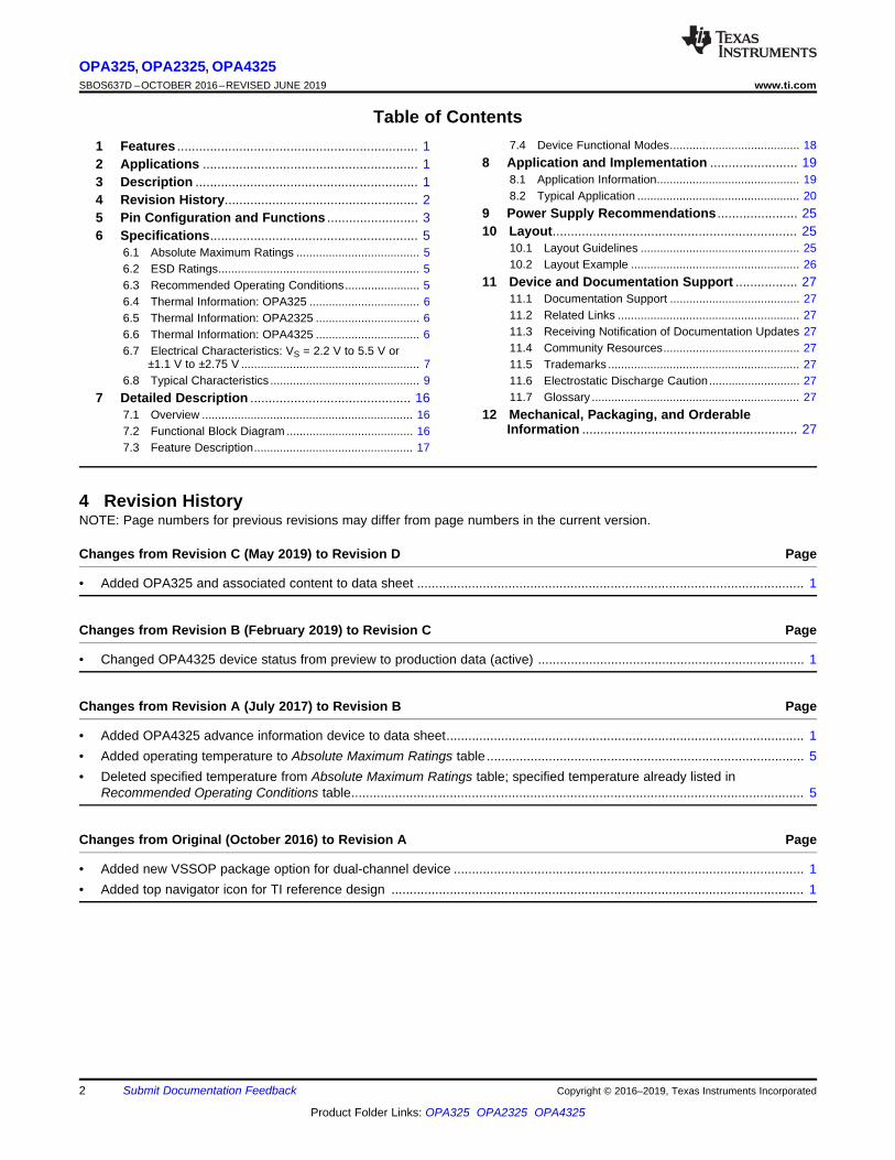
Typical Application (continued)The N-channel pair is active for input voltages close to the positive rail, typically (V+) – 1 V to 200 mV above thepositive supply, and the P-channel pair is on for inputs from 200 mV below the negative supply to approximately(V+) – 1 V. There is a small transition region, typically (V+) – 1.1 V to (V+) – 0.9 V, in which both pairs are on.This transition region is shown in Figure 48 for a traditional rail-to-rail input CMOS amplifier. Within this transitionregion, PSRR, CMRR, offset voltage, offset drift, and THD can be degraded when compared to device operationoutside of this region.
Figure 48. Input Offset Voltage vs Common-Mode Voltage(For Traditional Rail-to-Rail Input CMOS Amplifiers)
The OPAx325 amplifiers include an internal charge pump that powers the amplifier input stage with an internalsupply rail that is higher than the external power supply. The internal supply rail allows a single differential pair tooperate and to be linear across the entire input common-mode voltage range, as shown in Table 1.
Figure 49. Single Differential Input Pair with a Charge Pump (Zero-Crossover)
+
±
GND
2.5 V
-2.5 V
VOUT
4-VPP
Sine Wave
Typical CMOS rail-to-rail amplifiers
+
±
GND
+2.5 V
-2.5 V
VOUT
4 VPP
Sine Wave
OPAx325
±150
±125
±100
±75
±50
±25
0
25
50
75
100
125
150
±3 ±2 ±1 0 1 2 3
VO
S (�
V)
VCM (V) C003
VCM = ±2.85 V VCM = 2.85 V
23
OPA325, OPA2325, OPA4325www.ti.com SBOS637D –OCTOBER 2016–REVISED JUNE 2019
Product Folder Links: OPA325 OPA2325 OPA4325
Submit Documentation FeedbackCopyright © 2016–2019, Texas Instruments Incorporated
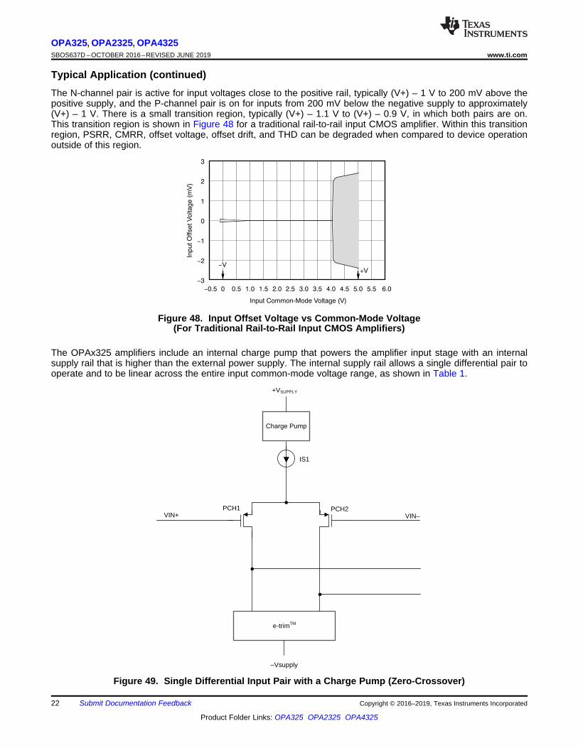
Typical Application (continued)The unique zero-crossover topology shown in Table 1 eliminates the input offset transition region, typical of mostrail-to-rail input operational amplifiers. This topology allows the OPAx325 to provide superior CMRR across theentire common-mode input range that extends 100 mV beyond both power-supply rails. Figure 50 shows theinput offset voltage versus input common-mode voltage plot for the OPAx325.
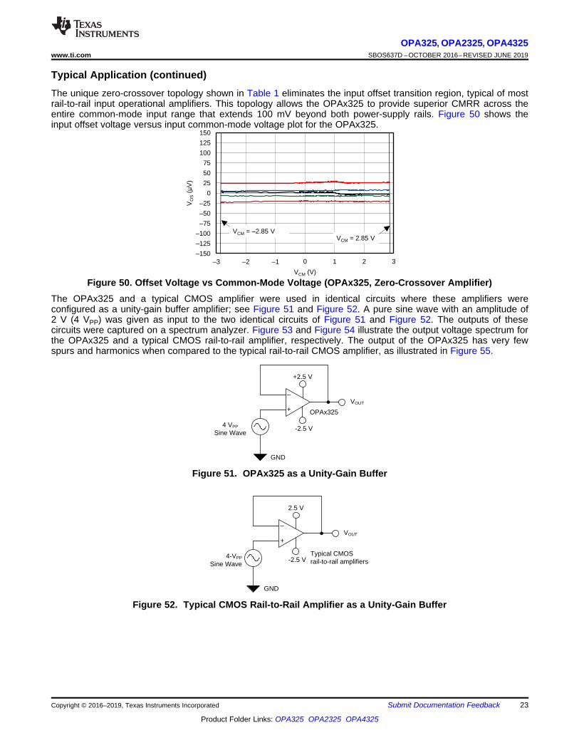
Figure 50. Offset Voltage vs Common-Mode Voltage (OPAx325, Zero-Crossover Amplifier)The OPAx325 and a typical CMOS amplifier were used in identical circuits where these amplifiers wereconfigured as a unity-gain buffer amplifier; see Figure 51 and Figure 52. A pure sine wave with an amplitude of2 V (4 VPP) was given as input to the two identical circuits of Figure 51 and Figure 52. The outputs of thesecircuits were captured on a spectrum analyzer. Figure 53 and Figure 54 illustrate the output voltage spectrum forthe OPAx325 and a typical CMOS rail-to-rail amplifier, respectively. The output of the OPAx325 has very fewspurs and harmonics when compared to the typical rail-to-rail CMOS amplifier, as illustrated in Figure 55.
Figure 51. OPAx325 as a Unity-Gain Buffer
Figure 52. Typical CMOS Rail-to-Rail Amplifier as a Unity-Gain Buffer

±120
±100
±80
±60
±40
±20
0
0. 5k 10k 15k 20k
TH
D +
N (
dB)
Frequency (Hz) C052
OPA2325
Typical rail-to-rail CMOS amplifier
±180
±160
±140
±120
±100
±80
±60
±40
±20
0
20
0. 5k 10k 15k 20k
Pow
er (
dB)
Frequency (Hz) C051
±180
±160
±140
±120
±100
±80
±60
±40
±20
0
20
0. 5k 10k 15k 20k
Pow
er (
dB)
Frequency (Hz) C053
24
OPA325, OPA2325, OPA4325SBOS637D –OCTOBER 2016–REVISED JUNE 2019 www.ti.com
Product Folder Links: OPA325 OPA2325 OPA4325
Submit Documentation Feedback Copyright © 2016–2019, Texas Instruments Incorporated
Typical Application (continued)8.2.3 Application Curves
Figure 53. Output Voltage Spectrum (OPAx325) Figure 54. Output Voltage Spectrum(Typical CMOS Rail-to-Rail Amplifier)
Figure 55. THD+N vs Frequency
25
OPA325, OPA2325, OPA4325www.ti.com SBOS637D –OCTOBER 2016–REVISED JUNE 2019
Product Folder Links: OPA325 OPA2325 OPA4325
Submit Documentation FeedbackCopyright © 2016–2019, Texas Instruments Incorporated
9 Power Supply RecommendationsThe OPAx325 are specified for operation from 2.2 V to 5.5 V (±1.1 V to ±2.75 V); many specifications apply from–40°C to +125°C. Parameters that can exhibit significant variance with regard to operating voltage ortemperature are presented in the Typical Characteristics section.
10 Layout
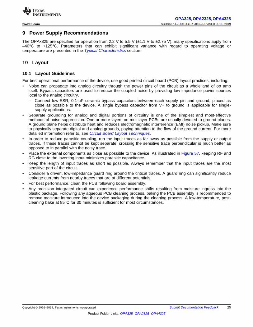
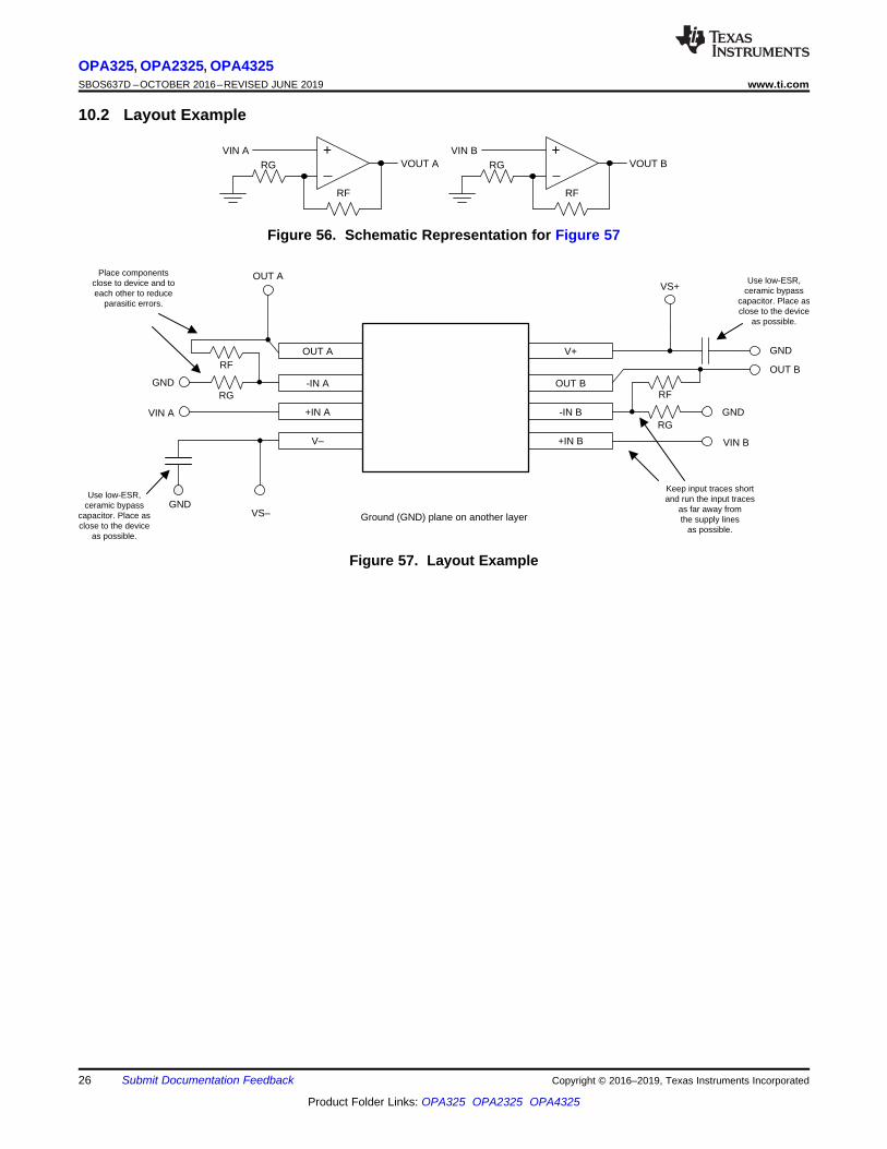
10.1 Layout GuidelinesFor best operational performance of the device, use good printed circuit board (PCB) layout practices, including:• Noise can propagate into analog circuitry through the power pins of the circuit as a whole and of op amp
itself. Bypass capacitors are used to reduce the coupled noise by providing low-impedance power sourceslocal to the analog circuitry.– Connect low-ESR, 0.1-µF ceramic bypass capacitors between each supply pin and ground, placed as
close as possible to the device. A single bypass capacitor from V+ to ground is applicable for single-supply applications.
• Separate grounding for analog and digital portions of circuitry is one of the simplest and most-effectivemethods of noise suppression. One or more layers on multilayer PCBs are usually devoted to ground planes.A ground plane helps distribute heat and reduces electromagnetic interference (EMI) noise pickup. Make sureto physically separate digital and analog grounds, paying attention to the flow of the ground current. For moredetailed information refer to, see Circuit Board Layout Techniques.
• In order to reduce parasitic coupling, run the input traces as far away as possible from the supply or outputtraces. If these traces cannot be kept separate, crossing the sensitive trace perpendicular is much better asopposed to in parallel with the noisy trace.
• Place the external components as close as possible to the device. As illustrated in Figure 57, keeping RF andRG close to the inverting input minimizes parasitic capacitance.
• Keep the length of input traces as short as possible. Always remember that the input traces are the mostsensitive part of the circuit.
• Consider a driven, low-impedance guard ring around the critical traces. A guard ring can significantly reduceleakage currents from nearby traces that are at different potentials.
• For best performance, clean the PCB following board assembly.• Any precision integrated circuit can experience performance shifts resulting from moisture ingress into the
plastic package. Following any aqueous PCB cleaning process, baking the PCB assembly is recommended toremove moisture introduced into the device packaging during the cleaning process. A low-temperature, post-cleaning bake at 85°C for 30 minutes is sufficient for most circumstances.
OUT A
-IN A
+IN A
V±
OUT B
-IN B
+IN B
V+
VS±GND
Ground (GND) plane on another layer
Keep input traces short and run the input traces
as far away fromthe supply lines
as possible.
Place components close to device and to each other to reduce
parasitic errors.
Use low-ESR, ceramic bypass
capacitor. Place as close to the device
as possible.
VIN A
GND
RF
RG
VIN B
GND
RF
RG
VS+
GND
OUT A
OUT B
Use low-ESR, ceramic bypass
capacitor. Place as close to the device
as possible.
+VIN BVOUT BRG
RF
+VIN AVOUT ARG
RF
26
OPA325, OPA2325, OPA4325SBOS637D –OCTOBER 2016–REVISED JUNE 2019 www.ti.com
Product Folder Links: OPA325 OPA2325 OPA4325
Submit Documentation Feedback Copyright © 2016–2019, Texas Instruments Incorporated
10.2 Layout Example
Figure 56. Schematic Representation for Figure 57
Figure 57. Layout Example

27
OPA325, OPA2325, OPA4325www.ti.com SBOS637D –OCTOBER 2016–REVISED JUNE 2019
Product Folder Links: OPA325 OPA2325 OPA4325
Submit Documentation FeedbackCopyright © 2016–2019, Texas Instruments Incorporated
11 Device and Documentation Support
11.1 Documentation Support
11.1.1 Related DocumentationFor related documentation see the following:
Texas Instruments, Circuit Board Layout Techniques application report
11.2 Related LinksTable 1 lists quick access links. Categories include technical documents, support and community resources,tools and software, and quick access to order now.
Table 1. Related Links
PARTS PRODUCT FOLDER ORDER NOW TECHNICALDOCUMENTS
TOOLS &SOFTWARE
SUPPORT &COMMUNITY
OPA325 Click here Click here Click here Click here Click hereOPA2325 Click here Click here Click here Click here Click hereOPA4325 Click here Click here Click here Click here Click here
11.3 Receiving Notification of Documentation UpdatesTo receive notification of documentation updates, navigate to the device product folder on ti.com. In the upperright corner, click on Alert me to register and receive a weekly digest of any product information that haschanged. For change details, review the revision history included in any revised document.
11.4 Community ResourcesThe following links connect to TI community resources. Linked contents are provided "AS IS" by the respectivecontributors. They do not constitute TI specifications and do not necessarily reflect TI's views; see TI's Terms ofUse.
TI E2E™ Online Community TI's Engineer-to-Engineer (E2E) Community. Created to foster collaborationamong engineers. At e2e.ti.com, you can ask questions, share knowledge, explore ideas and helpsolve problems with fellow engineers.
Design Support TI's Design Support Quickly find helpful E2E forums along with design support tools andcontact information for technical support.
11.5 Trademarkse-trim, E2E are trademarks of Texas Instruments.All other trademarks are the property of their respective owners.
11.6 Electrostatic Discharge CautionThis integrated circuit can be damaged by ESD. Texas Instruments recommends that all integrated circuits be handled withappropriate precautions. Failure to observe proper handling and installation procedures can cause damage.
ESD damage can range from subtle performance degradation to complete device failure. Precision integrated circuits may be moresusceptible to damage because very small parametric changes could cause the device not to meet its published specifications.
11.7 GlossarySLYZ022 — TI Glossary.
This glossary lists and explains terms, acronyms, and definitions.
12 Mechanical, Packaging, and Orderable InformationThe following pages include mechanical, packaging, and orderable information. This information is the mostcurrent data available for the designated devices. This data is subject to change without notice and revision ofthis document. For browser-based versions of this data sheet, refer to the left-hand navigation.

PACKAGE OPTION ADDENDUM
www.ti.com 10-Dec-2020
Addendum-Page 1
PACKAGING INFORMATION
Orderable Device Status(1)
Package Type PackageDrawing
Pins PackageQty
Eco Plan(2)
Lead finish/Ball material
(6)
MSL Peak Temp(3)
Op Temp (°C) Device Marking(4/5)
Samples
OPA2325ID ACTIVE SOIC D 8 75 RoHS & Green NIPDAU Level-2-260C-1 YEAR -40 to 125 O2325
OPA2325IDGKR ACTIVE VSSOP DGK 8 2500 RoHS & Green NIPDAUAG Level-2-260C-1 YEAR -40 to 125 18L6
OPA2325IDGKT ACTIVE VSSOP DGK 8 250 RoHS & Green NIPDAUAG Level-2-260C-1 YEAR -40 to 125 18L6
OPA2325IDR ACTIVE SOIC D 8 2500 RoHS & Green NIPDAU Level-2-260C-1 YEAR -40 to 125 O2325
OPA325IDBVR ACTIVE SOT-23 DBV 5 3000 RoHS & Green NIPDAU Level-2-260C-1 YEAR -40 to 125 1UEV
OPA325IDBVT ACTIVE SOT-23 DBV 5 250 RoHS & Green NIPDAU Level-2-260C-1 YEAR -40 to 125 1UEV
OPA4325IPW ACTIVE TSSOP PW 14 90 RoHS & Green NIPDAU Level-2-260C-1 YEAR -40 to 125 4325
OPA4325IPWR ACTIVE TSSOP PW 14 2000 RoHS & Green NIPDAU Level-2-260C-1 YEAR -40 to 125 4325
(1) The marketing status values are defined as follows:ACTIVE: Product device recommended for new designs.LIFEBUY: TI has announced that the device will be discontinued, and a lifetime-buy period is in effect.NRND: Not recommended for new designs. Device is in production to support existing customers, but TI does not recommend using this part in a new design.PREVIEW: Device has been announced but is not in production. Samples may or may not be available.OBSOLETE: TI has discontinued the production of the device.
(2) RoHS: TI defines "RoHS" to mean semiconductor products that are compliant with the current EU RoHS requirements for all 10 RoHS substances, including the requirement that RoHS substancedo not exceed 0.1% by weight in homogeneous materials. Where designed to be soldered at high temperatures, "RoHS" products are suitable for use in specified lead-free processes. TI mayreference these types of products as "Pb-Free".RoHS Exempt: TI defines "RoHS Exempt" to mean products that contain lead but are compliant with EU RoHS pursuant to a specific EU RoHS exemption.Green: TI defines "Green" to mean the content of Chlorine (Cl) and Bromine (Br) based flame retardants meet JS709B low halogen requirements of <=1000ppm threshold. Antimony trioxide basedflame retardants must also meet the <=1000ppm threshold requirement.
(3) MSL, Peak Temp. - The Moisture Sensitivity Level rating according to the JEDEC industry standard classifications, and peak solder temperature.
(4) There may be additional marking, which relates to the logo, the lot trace code information, or the environmental category on the device.
(5) Multiple Device Markings will be inside parentheses. Only one Device Marking contained in parentheses and separated by a "~" will appear on a device. If a line is indented then it is a continuationof the previous line and the two combined represent the entire Device Marking for that device.

PACKAGE OPTION ADDENDUM
www.ti.com 10-Dec-2020
Addendum-Page 2
(6) Lead finish/Ball material - Orderable Devices may have multiple material finish options. Finish options are separated by a vertical ruled line. Lead finish/Ball material values may wrap to twolines if the finish value exceeds the maximum column width.
Important Information and Disclaimer:The information provided on this page represents TI's knowledge and belief as of the date that it is provided. TI bases its knowledge and belief on informationprovided by third parties, and makes no representation or warranty as to the accuracy of such information. Efforts are underway to better integrate information from third parties. TI has taken andcontinues to take reasonable steps to provide representative and accurate information but may not have conducted destructive testing or chemical analysis on incoming materials and chemicals.TI and TI suppliers consider certain information to be proprietary, and thus CAS numbers and other limited information may not be available for release.
In no event shall TI's liability arising out of such information exceed the total purchase price of the TI part(s) at issue in this document sold by TI to Customer on an annual basis.
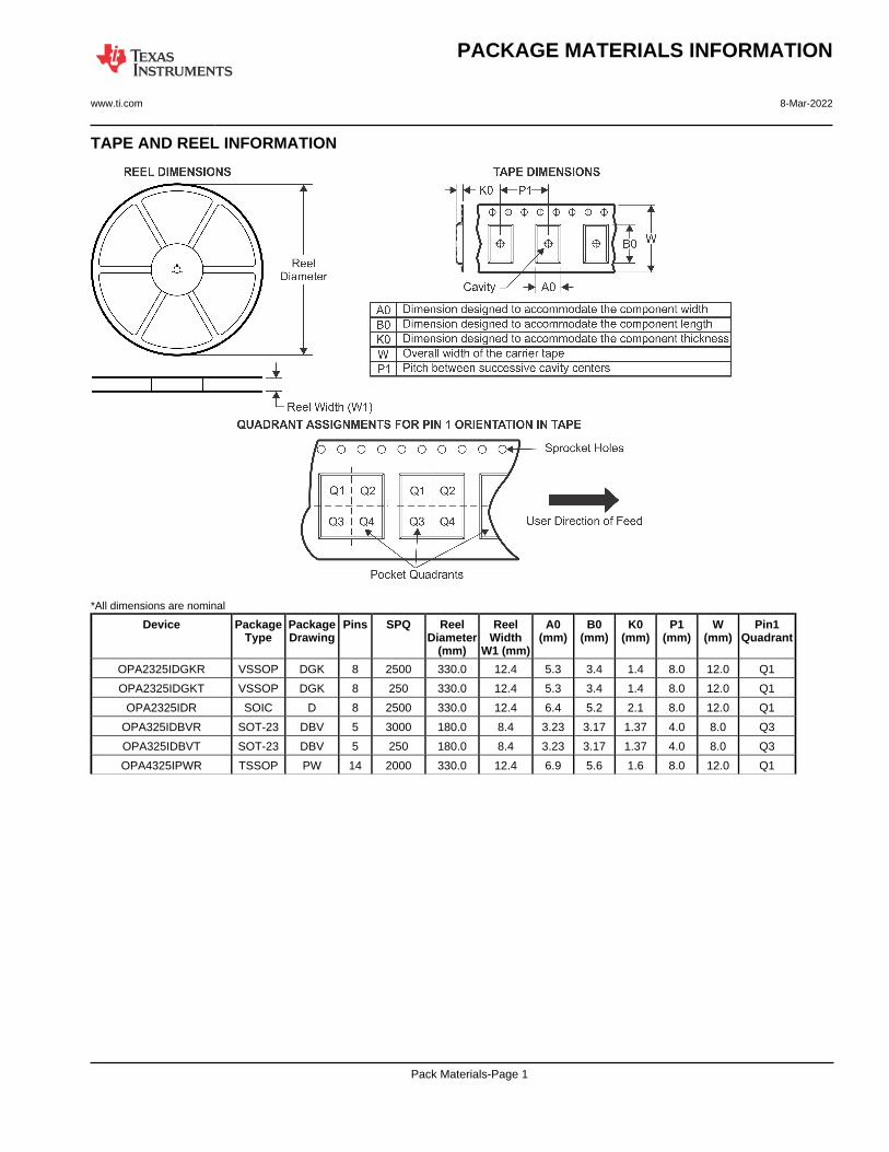
TAPE AND REEL INFORMATION
*All dimensions are nominal
Device PackageType
PackageDrawing
Pins SPQ ReelDiameter
(mm)
ReelWidth
W1 (mm)
A0(mm)
B0(mm)
K0(mm)
P1(mm)
W(mm)
Pin1Quadrant
OPA2325IDGKR VSSOP DGK 8 2500 330.0 12.4 5.3 3.4 1.4 8.0 12.0 Q1
OPA2325IDGKT VSSOP DGK 8 250 330.0 12.4 5.3 3.4 1.4 8.0 12.0 Q1
OPA2325IDR SOIC D 8 2500 330.0 12.4 6.4 5.2 2.1 8.0 12.0 Q1
OPA325IDBVR SOT-23 DBV 5 3000 180.0 8.4 3.23 3.17 1.37 4.0 8.0 Q3
OPA325IDBVT SOT-23 DBV 5 250 180.0 8.4 3.23 3.17 1.37 4.0 8.0 Q3
OPA4325IPWR TSSOP PW 14 2000 330.0 12.4 6.9 5.6 1.6 8.0 12.0 Q1
PACKAGE MATERIALS INFORMATION
www.ti.com 8-Mar-2022
Pack Materials-Page 1

*All dimensions are nominal
Device Package Type Package Drawing Pins SPQ Length (mm) Width (mm) Height (mm)
OPA2325IDGKR VSSOP DGK 8 2500 366.0 364.0 50.0
OPA2325IDGKT VSSOP DGK 8 250 366.0 364.0 50.0
OPA2325IDR SOIC D 8 2500 853.0 449.0 35.0
OPA325IDBVR SOT-23 DBV 5 3000 213.0 191.0 35.0
OPA325IDBVT SOT-23 DBV 5 250 213.0 191.0 35.0
OPA4325IPWR TSSOP PW 14 2000 853.0 449.0 35.0
PACKAGE MATERIALS INFORMATION
www.ti.com 8-Mar-2022
Pack Materials-Page 2

TUBE
*All dimensions are nominal
Device Package Name Package Type Pins SPQ L (mm) W (mm) T (µm) B (mm)
OPA2325ID D SOIC 8 75 506.6 8 3940 4.32
OPA4325IPW PW TSSOP 14 90 530 10.2 3600 3.5
PACKAGE MATERIALS INFORMATION
www.ti.com 8-Mar-2022
Pack Materials-Page 3

www.ti.com
PACKAGE OUTLINE
C
0.220.08 TYP
0.25
3.02.6
2X 0.95
1.9
1.450.90
0.150.00 TYP
5X 0.50.3
0.60.3 TYP
80 TYP
1.9
A
3.052.75
B1.751.45
(1.1)
SOT-23 - 1.45 mm max heightDBV0005ASMALL OUTLINE TRANSISTOR
4214839/F 06/2021
NOTES: 1. All linear dimensions are in millimeters. Any dimensions in parenthesis are for reference only. Dimensioning and tolerancing per ASME Y14.5M.2. This drawing is subject to change without notice.3. Refernce JEDEC MO-178.4. Body dimensions do not include mold flash, protrusions, or gate burrs. Mold flash, protrusions, or gate burrs shall not exceed 0.25 mm per side.
0.2 C A B
1
34
5
2
INDEX AREAPIN 1
GAGE PLANE
SEATING PLANE
0.1 C
SCALE 4.000
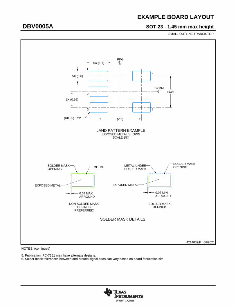
www.ti.com
EXAMPLE BOARD LAYOUT
0.07 MAXARROUND
0.07 MINARROUND
5X (1.1)
5X (0.6)
(2.6)
(1.9)
2X (0.95)
(R0.05) TYP
4214839/F 06/2021
SOT-23 - 1.45 mm max heightDBV0005ASMALL OUTLINE TRANSISTOR
NOTES: (continued) 5. Publication IPC-7351 may have alternate designs. 6. Solder mask tolerances between and around signal pads can vary based on board fabrication site.
SYMM
LAND PATTERN EXAMPLEEXPOSED METAL SHOWN
SCALE:15X
PKG
1
3 4
5
2
SOLDER MASKOPENINGMETAL UNDER
SOLDER MASK
SOLDER MASKDEFINED
EXPOSED METAL
METALSOLDER MASKOPENING
NON SOLDER MASKDEFINED
(PREFERRED)
SOLDER MASK DETAILS
EXPOSED METAL

www.ti.com
EXAMPLE STENCIL DESIGN
(2.6)
(1.9)
2X(0.95)
5X (1.1)
5X (0.6)
(R0.05) TYP
SOT-23 - 1.45 mm max heightDBV0005ASMALL OUTLINE TRANSISTOR
4214839/F 06/2021
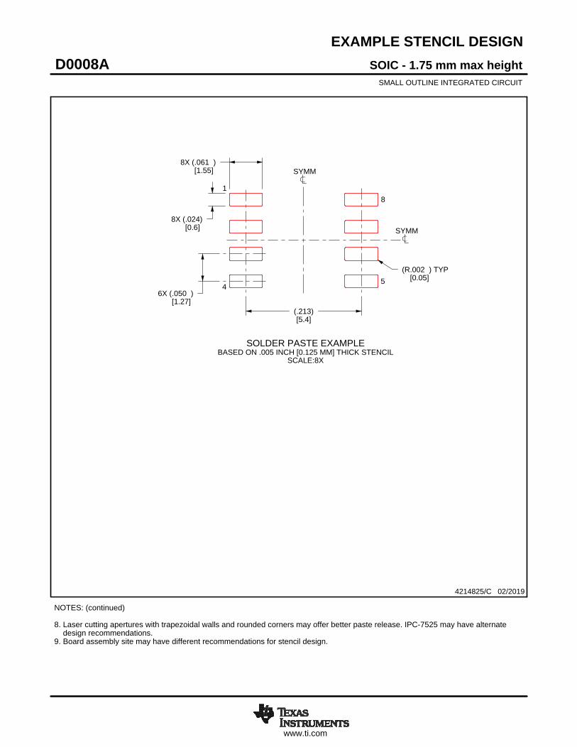
NOTES: (continued) 7. Laser cutting apertures with trapezoidal walls and rounded corners may offer better paste release. IPC-7525 may have alternate design recommendations. 8. Board assembly site may have different recommendations for stencil design.
SOLDER PASTE EXAMPLEBASED ON 0.125 mm THICK STENCIL
SCALE:15X
SYMM
PKG
1
3 4
5
2


www.ti.com
PACKAGE OUTLINE
C
.228-.244 TYP[5.80-6.19]
.069 MAX[1.75]
6X .050[1.27]
8X .012-.020 [0.31-0.51]
2X.150[3.81]
.005-.010 TYP[0.13-0.25]
0 - 8 .004-.010[0.11-0.25]
.010[0.25]
.016-.050[0.41-1.27]
4X (0 -15 )
A
.189-.197[4.81-5.00]
NOTE 3
B .150-.157[3.81-3.98]
NOTE 4
4X (0 -15 )
(.041)[1.04]
SOIC - 1.75 mm max heightD0008ASMALL OUTLINE INTEGRATED CIRCUIT
4214825/C 02/2019
NOTES: 1. Linear dimensions are in inches [millimeters]. Dimensions in parenthesis are for reference only. Controlling dimensions are in inches. Dimensioning and tolerancing per ASME Y14.5M. 2. This drawing is subject to change without notice. 3. This dimension does not include mold flash, protrusions, or gate burrs. Mold flash, protrusions, or gate burrs shall not exceed .006 [0.15] per side. 4. This dimension does not include interlead flash.5. Reference JEDEC registration MS-012, variation AA.
18
.010 [0.25] C A B
54
PIN 1 ID AREA
SEATING PLANE
.004 [0.1] C
SEE DETAIL A
DETAIL ATYPICAL
SCALE 2.800

www.ti.com
EXAMPLE BOARD LAYOUT
.0028 MAX[0.07]ALL AROUND
.0028 MIN[0.07]ALL AROUND
(.213)[5.4]
6X (.050 )[1.27]
8X (.061 )[1.55]
8X (.024)[0.6]
(R.002 ) TYP[0.05]
SOIC - 1.75 mm max heightD0008ASMALL OUTLINE INTEGRATED CIRCUIT
4214825/C 02/2019
NOTES: (continued) 6. Publication IPC-7351 may have alternate designs. 7. Solder mask tolerances between and around signal pads can vary based on board fabrication site.
METALSOLDER MASKOPENING
NON SOLDER MASKDEFINED
SOLDER MASK DETAILS
EXPOSEDMETAL
OPENINGSOLDER MASK METAL UNDER
SOLDER MASK
SOLDER MASKDEFINED
EXPOSEDMETAL
LAND PATTERN EXAMPLEEXPOSED METAL SHOWN
SCALE:8X
SYMM
1
45
8
SEEDETAILS
SYMM
www.ti.com
EXAMPLE STENCIL DESIGN
8X (.061 )[1.55]
8X (.024)[0.6]
6X (.050 )[1.27]
(.213)[5.4]
(R.002 ) TYP[0.05]
SOIC - 1.75 mm max heightD0008ASMALL OUTLINE INTEGRATED CIRCUIT
4214825/C 02/2019
NOTES: (continued) 8. Laser cutting apertures with trapezoidal walls and rounded corners may offer better paste release. IPC-7525 may have alternate design recommendations. 9. Board assembly site may have different recommendations for stencil design.
SOLDER PASTE EXAMPLEBASED ON .005 INCH [0.125 MM] THICK STENCIL
SCALE:8X
SYMM
SYMM
1
45
8

IMPORTANT NOTICE AND DISCLAIMERTI PROVIDES TECHNICAL AND RELIABILITY DATA (INCLUDING DATA SHEETS), DESIGN RESOURCES (INCLUDING REFERENCE DESIGNS), APPLICATION OR OTHER DESIGN ADVICE, WEB TOOLS, SAFETY INFORMATION, AND OTHER RESOURCES “AS IS” AND WITH ALL FAULTS, AND DISCLAIMS ALL WARRANTIES, EXPRESS AND IMPLIED, INCLUDING WITHOUT LIMITATION ANY IMPLIED WARRANTIES OF MERCHANTABILITY, FITNESS FOR A PARTICULAR PURPOSE OR NON-INFRINGEMENT OF THIRD PARTY INTELLECTUAL PROPERTY RIGHTS.These resources are intended for skilled developers designing with TI products. You are solely responsible for (1) selecting the appropriate TI products for your application, (2) designing, validating and testing your application, and (3) ensuring your application meets applicable standards, and any other safety, security, regulatory or other requirements.These resources are subject to change without notice. TI grants you permission to use these resources only for development of an application that uses the TI products described in the resource. Other reproduction and display of these resources is prohibited. No license is granted to any other TI intellectual property right or to any third party intellectual property right. TI disclaims responsibility for, and you will fully indemnify TI and its representatives against, any claims, damages, costs, losses, and liabilities arising out of your use of these resources.TI’s products are provided subject to TI’s Terms of Sale or other applicable terms available either on ti.com or provided in conjunction with such TI products. TI’s provision of these resources does not expand or otherwise alter TI’s applicable warranties or warranty disclaimers for TI products.TI objects to and rejects any additional or different terms you may have proposed. IMPORTANT NOTICE
Mailing Address: Texas Instruments, Post Office Box 655303, Dallas, Texas 75265Copyright © 2022, Texas Instruments Incorporated
Related Documents