On the geometrical and electronic structure of an ultra-thin crystalline silica film grown on Mo(1 1 2) S. Kaya a , M. Baron a , D. Stacchiola a , J. Weissenrieder a , S. Shaikhutdinov a, * , T.K. Todorova b , M. Sierka b, * , J. Sauer b , H.-J. Freund a a Fritz-Haber-Institut der Max-Planck-Gesellschaft, Faradayweg 4-6, 14195 Berlin, Germany b Humboldt-Universita ¨ t zu Berlin, Institut fu ¨ r Chemie, Unter den Linden 6, 10099 Berlin, Germany Received 26 April 2007; accepted for publication 31 July 2007 Available online 25 August 2007 Abstract The atomic structure of a well-ordered silica film grown on a Mo(1 1 2) single crystal substrate is discussed in detail using the exper- imental and theoretical results available to date. New photoelectron spectroscopy results using synchrotron radiation and ultraviolet spectroscopy data are presented. The analysis unambiguously shows that the ultra-thin silica film consists of a two-dimensional network of corner-sharing [SiO 4 ] tetrahedra chemisorbed on the unreconstructed Mo(1 1 2) surface. The review also highlights the important role of theoretical calculations in the determination of the atomic structure of the silica films and in interpretation of experimental data. Ó 2007 Elsevier B.V. All rights reserved. Keywords: Thin oxide films; Oxide surfaces; Silica; Scanning tunneling microscopy; Vibrational spectroscopy; Photoelectron spectroscopy; Density functional theory 1. Introduction In recent years, thin oxide films have received much interest due to their potential use in many technological applications such as insulating layers in integrated circuits, protective films against corrosion, and supports for metal nanoparticles in sensors and catalysts. When grown on me- tal substrates, oxide films are well suited for studying elec- tronic and chemical properties by a variety of surface sensitive techniques. This ‘‘surface science’’ approach has been proven to be very efficient for determining the atomic structure of many oxide surfaces (see [1–12] and references therein). Silica (SiO 2 ) is one of the most important oxides in ad- vanced technology. Although the first attempts to synthe- size crystalline silica films can be traced back to the early 90’s [13,14], the preparation of well-ordered thin silica films was reported only recently by Schroeder et al. [15–18] using a Mo(1 1 2) substrate, who basically modified a recipe orig- inally applied to the Mo(1 0 0) and Mo(1 1 0) substrates by Goodman and co-workers [13,14]. The film exhibited a c(2 · 2) diffraction pattern with respect to Mo(1 1 2), and showed at least two oxygen species in X-ray photoelectron spectra (XPS) and a strong phonon absorption band cen- tered at 1048 cm 1 observed by infrared reflection absorp- tion spectroscopy (IRAS). During the last five years there have been numerous experimental and theoretical efforts in order to elucidate the atomic structure of these films and employ their use as model supports for metal (Pd, Au, Ag) particles [19–45]. Based on attenuation of the substrate signals in Auger electron spectroscopy (AES) and angular-resolved XPS spectra, Schroeder et al. [15] came to the conclusion that the well-ordered films are 5–8 A ˚ in thickness. Based on AES data Kim et al. [24] also reported on the film thickness of 7–8 A ˚ . Later the same group, using another preparation, 0039-6028/$ - see front matter Ó 2007 Elsevier B.V. All rights reserved. doi:10.1016/j.susc.2007.07.030 * Corresponding authors. Tel.: +49 30 8413 4114; fax: +49 30 8413 4105. E-mail addresses: [email protected] (S. Shaikhutdi- nov), [email protected] (M. Sierka). www.elsevier.com/locate/susc Available online at www.sciencedirect.com Surface Science 601 (2007) 4849–4861

Welcome message from author
This document is posted to help you gain knowledge. Please leave a comment to let me know what you think about it! Share it to your friends and learn new things together.
Transcript
Available online at www.sciencedirect.com
www.elsevier.com/locate/susc
Surface Science 601 (2007) 4849–4861
On the geometrical and electronic structure of an ultra-thincrystalline silica film grown on Mo(112)
S. Kaya a, M. Baron a, D. Stacchiola a, J. Weissenrieder a, S. Shaikhutdinov a,*,T.K. Todorova b, M. Sierka b,*, J. Sauer b, H.-J. Freund a
a Fritz-Haber-Institut der Max-Planck-Gesellschaft, Faradayweg 4-6, 14195 Berlin, Germanyb Humboldt-Universitat zu Berlin, Institut fur Chemie, Unter den Linden 6, 10099 Berlin, Germany
Received 26 April 2007; accepted for publication 31 July 2007Available online 25 August 2007
Abstract
The atomic structure of a well-ordered silica film grown on a Mo(112) single crystal substrate is discussed in detail using the exper-imental and theoretical results available to date. New photoelectron spectroscopy results using synchrotron radiation and ultravioletspectroscopy data are presented. The analysis unambiguously shows that the ultra-thin silica film consists of a two-dimensional networkof corner-sharing [SiO4] tetrahedra chemisorbed on the unreconstructed Mo(112) surface. The review also highlights the important roleof theoretical calculations in the determination of the atomic structure of the silica films and in interpretation of experimental data.� 2007 Elsevier B.V. All rights reserved.
Keywords: Thin oxide films; Oxide surfaces; Silica; Scanning tunneling microscopy; Vibrational spectroscopy; Photoelectron spectroscopy; Densityfunctional theory
1. Introduction
In recent years, thin oxide films have received muchinterest due to their potential use in many technologicalapplications such as insulating layers in integrated circuits,protective films against corrosion, and supports for metalnanoparticles in sensors and catalysts. When grown on me-tal substrates, oxide films are well suited for studying elec-tronic and chemical properties by a variety of surfacesensitive techniques. This ‘‘surface science’’ approach hasbeen proven to be very efficient for determining the atomicstructure of many oxide surfaces (see [1–12] and referencestherein).
Silica (SiO2) is one of the most important oxides in ad-vanced technology. Although the first attempts to synthe-size crystalline silica films can be traced back to the early
0039-6028/$ - see front matter � 2007 Elsevier B.V. All rights reserved.
doi:10.1016/j.susc.2007.07.030
* Corresponding authors. Tel.: +49 30 8413 4114; fax: +49 30 8413 4105.E-mail addresses: [email protected] (S. Shaikhutdi-
nov), [email protected] (M. Sierka).
90’s [13,14], the preparation of well-ordered thin silica filmswas reported only recently by Schroeder et al. [15–18] usinga Mo(112) substrate, who basically modified a recipe orig-inally applied to the Mo(100) and Mo(11 0) substrates byGoodman and co-workers [13,14]. The film exhibited ac(2 · 2) diffraction pattern with respect to Mo(112), andshowed at least two oxygen species in X-ray photoelectronspectra (XPS) and a strong phonon absorption band cen-tered at 1048 cm�1 observed by infrared reflection absorp-tion spectroscopy (IRAS). During the last five years therehave been numerous experimental and theoretical effortsin order to elucidate the atomic structure of these filmsand employ their use as model supports for metal (Pd,Au, Ag) particles [19–45].
Based on attenuation of the substrate signals in Augerelectron spectroscopy (AES) and angular-resolved XPSspectra, Schroeder et al. [15] came to the conclusion thatthe well-ordered films are 5–8 A in thickness. Based onAES data Kim et al. [24] also reported on the film thicknessof 7–8 A. Later the same group, using another preparation,
4850 S. Kaya et al. / Surface Science 601 (2007) 4849–4861
concluded from the AES results that the film is only 3 A inthickness [28].
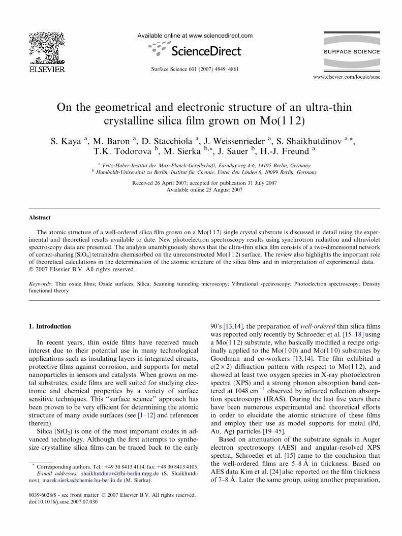
In the first structural model proposed by Schroeder et al.[18], the film was bonded to the Mo substrate through threeoxygen atoms sitting in pseudo three-fold hollow sitesformed between protruding and trough Mo atoms, formingrows on the Mo(11 2) surface along the ½�1�11� direction.These sites were suggested as the most stable for oxygenchemisorption on Mo surfaces. Assuming that a [SiO4] tet-rahedron is the building unit for the silica films, the pro-posed structure involved a maximum coordination ofoxygen atoms to the Mo surface, i.e. three O atoms of eachtetrahedra were bonded to the Mo atoms. In this model,the forth (‘‘apical’’) oxygen atom of each tetrahedra (whichremains uncoordinated in the case of a monolayer silica
Fig. 1. Different models proposed for the monolayer silica film grown on MoShown in the (c) and (d) are ‘‘2D-network’’ models for the ‘‘O-poor’’ and ‘‘O
film) must be stabilized either by hydrogen, thus formingsilanol (Si–OH) groups, or shared with further silica layers.Since neither silanol nor hydroxyl species were observed onthese films [18], this implied that the silica film was of sev-eral layers in thickness.
Following this model and assuming that the film isthree layers of SiO2, Ricci and Pacchioni [27] proposed ab-cristobalite derived structure as thermodynamically themost stable. In particular, formation of two-memberedrings were invoked to explain a weak vibration bandaround 795 cm�1 experimentally observed by Schroederet al. [18].
However, Chen et al. [28], analyzing high-resolutionelectron energy loss spectra (HREELS) of the silica filmsand various Si and Mo oxide compounds available in the
(112). (a, b) ‘‘Cluster models’’ as suggested in Ref. [28] (a) and [43] (b).-rich’’ films, respectively [32,37].
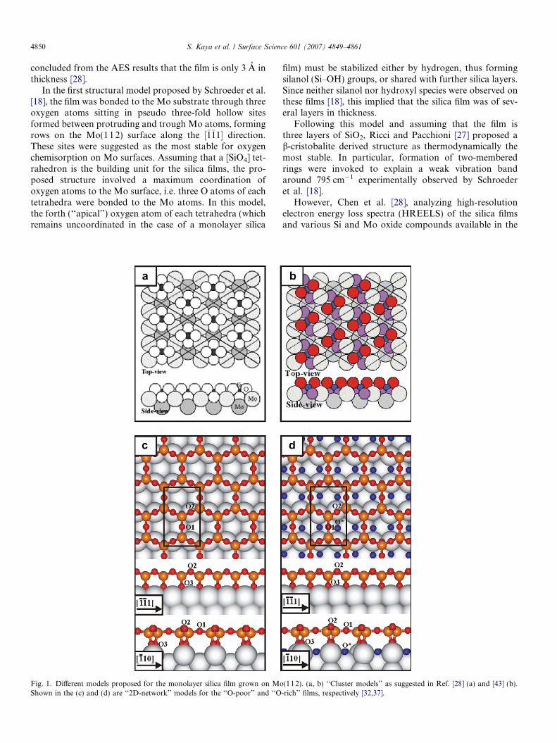
Fig. 2. Large-scale (a) and atomically resolved (b, d) STM images of the ‘‘O-poor’’ silica films together with the image simulation of the model shown inFig. 1c. (b) High-resolution image of antiphase domain boundaries, indicated by the arrows in (a), is superimposed with the APDB model shown in (e).The atomic protrusions seen in (b) and (d) represent the Si and O atoms, respectively. The crystal directions shown in (a) are applied to all figures except(c). The STM image reported in [43] is shown in (c), for comparison. DFT-optimized geometry and simulated STM image for the cluster models are shownin (f) and (g). The size and tunnelling parameters are: (a) 14 · 14 nm2; V = 1.3 V, I = 0.45 nA; (b) 3.2 · 3.2 nm2; 1.2 V, 0.35 nA; (c) 5.5 · 5.5 nm2; �3 V,0.3 nA; (d) 3 · 2.25 nm2; 0.65 V, 0.75 nA.
S. Kaya et al. / Surface Science 601 (2007) 4849–4861 4851
literature, have suggested that the most prominent absorp-tion band at 1048 cm�1 observed on the film must be as-signed to the Si–O–Mo vibration. The absence of theband in the 1150–1200 cm�1 region, characteristic for theSi–O–Si asymmetric stretching in the bulk silica systems,led the authors to the conclusion that the film does not ex-hibit Si–O–Si bonds. Therefore, the authors have proposeda model consisting of a layer of isolated [SiO4] clusters ar-ranged in a c(2 · 2) structure on the Mo(112) surface withall oxygen atoms bonding to the Mo substrate as shown inFig. 1a. This model is hereafter referred to as a ‘‘clustermodel’’.
The interest in the structure of ultra-thin films was rein-forced after Weissenrieder et al. [32], modifying the prepa-ration procedure, reported a scanning tunnelingmicroscopy (STM) study of the silica films with atomic res-olution. The STM images revealed a honeycomb-like sur-face on the extended flat terraces separated by themonoatomic steps of the Mo substrate underneath(Fig. 2a). In addition, well-resolved images of antiphasedomain boundaries (APDB) running along the ½�110� direc-tion as predicted by LEED studies [18] were obtained asindicated in Fig. 2a. Density functional theory (DFT),combined with IRAS and XPS data (discussed below) ob-tained on the same samples, have shown that the film is in-deed of a monolayer thickness but consists of [SiO4]tetrahedra with one apex O atom pointing to the Mo sur-face, whereas the surface is formed by a fully saturated Olayer arranged in honeycomb structure through sharingthe corner O-atoms (see Fig. 1c) [32,36]. (Note, that thisstructure was suggested but rejected by Chen et al [28].)This model is henceforth referred to as the ‘‘2D-networkmodel’’. Simultaneously, a similar 2D-network model of
the film was independently proposed by Pacchioni andco-workers [33] who also discarded the cluster model forthe silica film.
However, very recently, Chen and Goodman [43] re-ported an STM study, which in their opinion favors thecluster model, although slightly modified as shown inFig. 1b. In addition, they discussed issues in interpretingvibrational spectra of thin films and referred to the clustercalculations of Yakovkin [34].
In this paper, we have attempted to critically review allthe experimental and theoretical studies on thin crystallinesilica films reported to date. In addition, we provide newphotoelectron spectroscopy results using synchrotron radi-ation and also report an UPS study, which strongly sup-port the 2D-network model of the monolayer silica film.This review also highlights the crucial role of theory inthe determination of atomic structure of the silica filmsand in interpretation of their vibrational spectra.
This paper was organized as follows. We first describethe details of the silica film preparation, which turn outto be critical for the structures of the films grown. Thenwe summarize the key observations of experimental andtheoretical studies on this system reported in the literatureand discuss how these results agree or disagree with themodels suggested. The paper ends with a summary andconcluding remarks.
2. Film preparation
There are different preparations of the silica film onMo(112) reported in the literature. Originally, Schroederet al. [15] used four cycles of Si deposition at 300 K andoxidation at 800 K in 5 · 10�6 mbar O2. Subsequently,
4852 S. Kaya et al. / Surface Science 601 (2007) 4849–4861
the film was annealed stepwise up to 1100–1250 K in 10�5
mbar of O2 until the films exhibited a c(2 · 2)-Mo(112)structure by LEED.
Chen et al. [28] have modified the recipe by first expos-ing a clean Mo(112) surface to 5 · 10�8 mbar O2 at 850 K,which produces the p(2 · 3)O–Mo(112) surface. Sub-monolayer amounts of Si were then deposited onto thissurface at 300 K, followed by annealing at 800 K in10�7 mbar O2 for 5 min and increasing the temperatureto 1200 K for additional 5 min. These steps were repeatedseveral times until a constant Si/Mo Auger ratio was ob-tained. Another preparation basically omitted the interme-diate annealing step, and only the completed film wassubjected to annealing at temperatures that range from1000 to 1200 K. In addition to these ‘‘multistep’’ prepara-tions, the same group later used a single step preparationby deposition of 1.5–2 monolayer (ML) of Si onto thep(2 · 3)O–Mo(112) surface at 300 K followed by oxidationin 10�7 mbar O2 at 800 K for 10 min and annealing at1050–1250 K using the same oxygen pressures.
Finally, our own group prepared the films by exposingthe clean Mo(112) surface to 5 · 10�8 mbar O2 at 900 K(resulting in p(2 · 3)O–Mo(112) surface) and subsequentdeposition of approximately 1.2 ML of Si at the same oxy-gen pressure and temperature. The films were then an-nealed in UHV at ca. 1250 K. The annealing temperaturehas turned out to be critical. Based on the STM studieswe have found that overheating results in partial sublima-tion of the film, while low temperature annealing results inthe presence of ill-defined silica particles on top of the or-dered film. The preparation involving final annealing inUHV produces the film, which is referred to as ‘‘O-poor’’.In contrast, high temperature annealing in �10�6 mbar O2
during the preparation or, alternatively, annealing of the‘‘O-poor’’ films in oxygen results in the ‘‘O-rich’’ films, inwhich additional oxygen atoms underneath the film are ad-sorbed onto the Mo substrate [37] (see Fig. 1d). Therefore,the preparations reported by Schroeder et al. [15] and Chenet al. [28], which include annealing in oxygen ambient,must have resulted in the ‘‘O-rich’’ films in our notation.
3. Low energy electron diffraction (LEED)
All well-ordered silica films prepared by different recipesshowed a c(2 · 2)-Mo(112) diffraction pattern. Chen et al.[28] depicted several possible models which may explain thec(2 · 2) structure. In principle, both cluster and 2D-net-work models exhibit this symmetry. Note, however, thata spot-profile analysis of the diffraction patterns performedby Schroeder et al. [18] revealed a structure containing twodomains with antiphase domain boundaries (APDB) be-tween the domains propagating along the ½�110� direction.
The presence of additional oxygen atoms observed inthe ‘‘O-rich’’ films does not change the symmetry of thefilm and cannot be discerned by conventional LEED. Tothe best of our knowledge, no dynamic (I/V) LEED studiesare reported to date.
4. Scanning tunneling microscopy (STM)
Determination of the atomic structure of the monolayersilica film using electron and vibrational spectroscopies,which will be discussed in the following sections, cannotbe done without precise control of the morphology of thesilica films under study, even though LEED may show asharp diffraction pattern. In particular, the samples maycontain small silica particles and clusters, whose propertiesmay strongly influence the spectroscopic results. The sys-tematic STM studies performed in [36] revealed that atom-ically flat films can be produced only after annealing attemperatures above 1200 K. It should be also emphasizedthat STM images of the thin oxide films very often cannotbe interpreted straightforwardly and therefore other sup-porting information is necessary to prove a proposed struc-ture model (see, for example, [9,12]).
Figs. 2b and 2d show high-resolution STM images ob-tained on the ‘‘O-poor’’ films. A honeycomb-like structureresolved in Fig. 2d was explained within the 2D-networkmodel by assigning the protrusions in this image to theoxygen atoms in the topmost O-layer. Indeed, the imagesimulation performed on the basis of the calculated densityof states for this structure showed a good match with theexperiment (Fig. 2). Furthermore, at certain tunnelingparameters the Si atoms could be imaged (Fig. 2b) and,again, this fact has been proven by comparing the experi-mental and simulated STM images [32,36].
Fig. 2 also shows the line defects running along the Mo½�110� direction, as previously observed by LEED [18],which appear as alternating 8-members and 4-membersrings. These straight-line defects can be easily explainedwithin the 2D-network model by a half-lattice shift in the½�1�11� direction between two domains as shown in Fig. 2e.In contrast, the cluster model will result in the APDB run-ning in the ½�311� direction, which is inconsistent with theLEED results.
Interestingly, high-resolution images also showed modu-lation in corrugation amplitude on a large scale (seeFig. 2a). In a first approximation, this can be explainedas a result of the small lattice mismatch between the oxidefilm and the substrate, which often leads to the periodicMoire structure as observed for monolayer films of FeO/Pt [46], TiOx/Pt [47], Nb2O5/Cu3Au [48], etc. However, inthe case of silica, one should take into account a high flex-ibility of the Si–O–Si bonds that may explain the ‘‘randomwave’’ modulation observed. Another explanation is basedon the presence of small amounts of the sub-surface impu-rities in the Mo crystal.
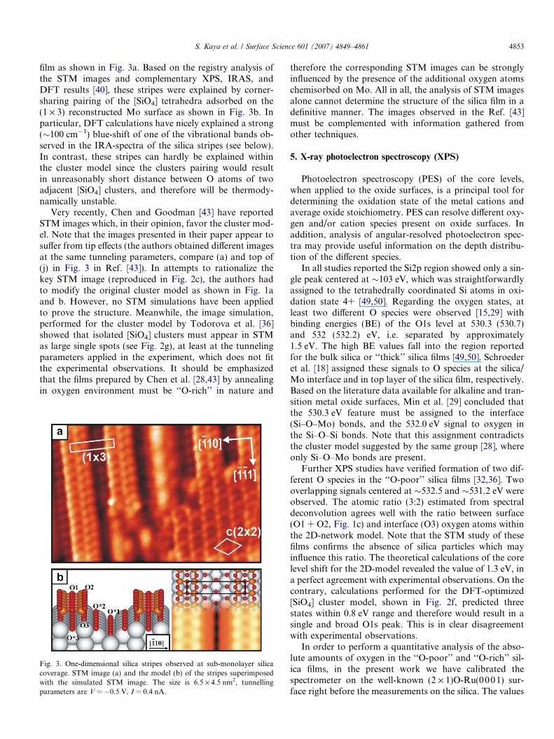
At sub-monolayer coverage, high-resolution STM stud-ies revealed formation of 0.5 nm-wide silica stripes alongthe ½�1�11� direction. These stripes, which exhibit a (1 · 3)periodicity, cannot be assigned to the oxygen reconstructedMo(112) surface which showed completely different STMimages on the Si-free samples prepared under the sameconditions in the blank experiments. The stripes coalesceand form islands with the same structure as the dense silica
S. Kaya et al. / Surface Science 601 (2007) 4849–4861 4853
film as shown in Fig. 3a. Based on the registry analysis ofthe STM images and complementary XPS, IRAS, andDFT results [40], these stripes were explained by corner-sharing pairing of the [SiO4] tetrahedra adsorbed on the(1 · 3) reconstructed Mo surface as shown in Fig. 3b. Inparticular, DFT calculations have nicely explained a strong(�100 cm�1) blue-shift of one of the vibrational bands ob-served in the IRA-spectra of the silica stripes (see below).In contrast, these stripes can hardly be explained withinthe cluster model since the clusters pairing would resultin unreasonably short distance between O atoms of twoadjacent [SiO4] clusters, and therefore will be thermody-namically unstable.
Very recently, Chen and Goodman [43] have reportedSTM images which, in their opinion, favor the cluster mod-el. Note that the images presented in their paper appear tosuffer from tip effects (the authors obtained different imagesat the same tunneling parameters, compare (a) and top of(j) in Fig. 3 in Ref. [43]). In attempts to rationalize thekey STM image (reproduced in Fig. 2c), the authors hadto modify the original cluster model as shown in Fig. 1aand b. However, no STM simulations have been appliedto prove the structure. Meanwhile, the image simulation,performed for the cluster model by Todorova et al. [36]showed that isolated [SiO4] clusters must appear in STMas large single spots (see Fig. 2g), at least at the tunnelingparameters applied in the experiment, which does not fitthe experimental observations. It should be emphasizedthat the films prepared by Chen et al. [28,43] by annealingin oxygen environment must be ‘‘O-rich’’ in nature and
Fig. 3. One-dimensional silica stripes observed at sub-monolayer silicacoverage. STM image (a) and the model (b) of the stripes superimposedwith the simulated STM image. The size is 6.5 · 4.5 nm2, tunnellingparameters are V = �0.5 V, I = 0.4 nA.
therefore the corresponding STM images can be stronglyinfluenced by the presence of the additional oxygen atomschemisorbed on Mo. All in all, the analysis of STM imagesalone cannot determine the structure of the silica film in adefinitive manner. The images observed in the Ref. [43]must be complemented with information gathered fromother techniques.
5. X-ray photoelectron spectroscopy (XPS)
Photoelectron spectroscopy (PES) of the core levels,when applied to the oxide surfaces, is a principal tool fordetermining the oxidation state of the metal cations andaverage oxide stoichiometry. PES can resolve different oxy-gen and/or cation species present on oxide surfaces. Inaddition, analysis of angular-resolved photoelectron spec-tra may provide useful information on the depth distribu-tion of the different species.
In all studies reported the Si2p region showed only a sin-gle peak centered at �103 eV, which was straightforwardlyassigned to the tetrahedrally coordinated Si atoms in oxi-dation state 4+ [49,50]. Regarding the oxygen states, atleast two different O species were observed [15,29] withbinding energies (BE) of the O1s level at 530.3 (530.7)and 532 (532.2) eV, i.e. separated by approximately1.5 eV. The high BE values fall into the region reportedfor the bulk silica or ‘‘thick’’ silica films [49,50]. Schroederet al. [18] assigned these signals to O species at the silica/Mo interface and in top layer of the silica film, respectively.Based on the literature data available for alkaline and tran-sition metal oxide surfaces, Min et al. [29] concluded thatthe 530.3 eV feature must be assigned to the interface(Si–O–Mo) bonds, and the 532.0 eV signal to oxygen inthe Si–O–Si bonds. Note that this assignment contradictsthe cluster model suggested by the same group [28], whereonly Si–O–Mo bonds are present.
Further XPS studies have verified formation of two dif-ferent O species in the ‘‘O-poor’’ silica films [32,36]. Twooverlapping signals centered at �532.5 and �531.2 eV wereobserved. The atomic ratio (3:2) estimated from spectraldeconvolution agrees well with the ratio between surface(O1 + O2, Fig. 1c) and interface (O3) oxygen atoms withinthe 2D-network model. Note that the STM study of thesefilms confirms the absence of silica particles which mayinfluence this ratio. The theoretical calculations of the corelevel shift for the 2D-model revealed the value of 1.3 eV, ina perfect agreement with experimental observations. On thecontrary, calculations performed for the DFT-optimized[SiO4] cluster model, shown in Fig. 2f, predicted threestates within 0.8 eV range and therefore would result in asingle and broad O1s peak. This is in clear disagreementwith experimental observations.
In order to perform a quantitative analysis of the abso-lute amounts of oxygen in the ‘‘O-poor’’ and ‘‘O-rich’’ sil-ica films, in the present work we have calibrated thespectrometer on the well-known (2 · 1)O-Ru(0001) sur-face right before the measurements on the silica. The values
4854 S. Kaya et al. / Surface Science 601 (2007) 4849–4861
measured (24 ± 4 and 28 ± 5 at/nm2, respectively) are con-sistent with the values predicted by the 2D-network model(=20.6 and 28.8 at/nm2) and far above the amount pre-dicted by the cluster model (=16.5 at/nm2).
The presence of ‘‘extra’’ oxygen atoms in the ‘‘O-rich’’films manifests itself in the feature at 530.6 eV [37], i.e.,close to that observed on the O/Mo(1 12) surface underthe same conditions (see also [51]). This feature overlapswith the signal of interface (Si–O–Mo) oxygen at531.2 eV. In addition, a high BE shoulder was observedin the Mo3d region [37], which was explained by a largercharge transfer through the O–Mo bond as compared tothe Si–O–Mo bonds.
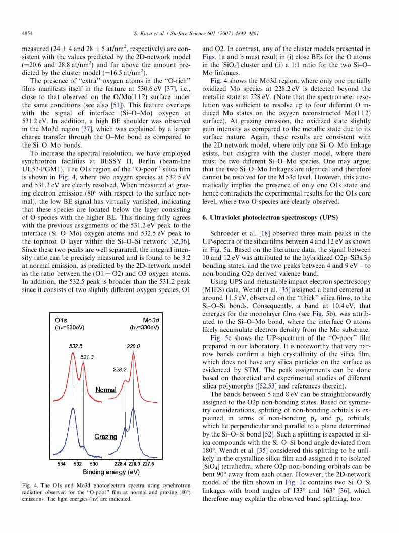
To increase the spectral resolution, we have employedsynchrotron facilities at BESSY II, Berlin (beam-lineUE52-PGM1). The O1s region of the ‘‘O-poor’’ silica filmis shown in Fig. 4, where two oxygen species at 532.5 eVand 531.2 eV are clearly resolved. When measured at graz-ing electron emission (80� with respect to the surface nor-mal), the low BE signal has virtually vanished, indicatingthat these species are located below the layer consistingof O species with the higher BE. This finding fully agreeswith the previous assignments of the 531.2 eV peak to theinterface (Si–O–Mo) oxygen atoms and 532.5 eV peak tothe topmost O layer within the Si–O–Si network [32,36].Since these two peaks are well separated, the integral inten-sity ratio can be precisely measured and is found to be 3:2at normal emission, as predicted by the 2D-network modelas the ratio between the (O1 + O2) and O3 oxygen atoms.In addition, the 532.5 peak is broader than the 531.2 peaksince it consists of two slightly different oxygen species, O1
Fig. 4. The O1s and Mo3d photoelectron spectra using synchrotronradiation observed for the ‘‘O-poor’’ film at normal and grazing (80�)emissions. The light energies (hm) are indicated.
and O2. In contrast, any of the cluster models presented inFigs. 1a and b must result in (i) close BEs for the O atomsin the [SiO4] cluster and (ii) a 1:1 ratio for the two Si–O–Mo linkages.
Fig. 4 shows the Mo3d region, where only one partiallyoxidized Mo species at 228.2 eV is detected beyond themetallic state at 228 eV. (Note that the spectrometer reso-lution was sufficient to resolve up to four different O in-duced Mo states on the oxygen reconstructed Mo(112)surface). At grazing emission, the oxidized state slightlygain intensity as compared to the metallic state due to itssurface nature. Again, these results are consistent withthe 2D-network model, where only one Si–O–Mo linkageexists, but disagree with the cluster model, where theremust be two different Si–O–Mo species. One may argue,that the two Si–O–Mo linkages are identical and thereforecannot be resolved for the Mo3d level. However, this auto-matically implies the presence of only one O1s state andhence contradicts the experimental results for the O1s corelevel, where two O species are clearly observed.
6. Ultraviolet photoelectron spectroscopy (UPS)
Schroeder et al. [18] observed three main peaks in theUP-spectra of the silica films between 4 and 12 eV as shownin Fig. 5a. Based on the literature data, the signal between10 and 12 eV was attributed to the hybridized O2p–Si3s,3pbonding states, and the two peaks between 4 and 9 eV – tonon-bonding O2p derived valence band.
Using UPS and metastable impact electron spectroscopy(MIES) data, Wendt et al. [35] assigned a band centered ataround 11.5 eV, observed on the ‘‘thick’’ silica films, to theSi–O–Si bonds. Consequently, a band at 10.4 eV, thatemerges for the monolayer films (see Fig. 5b), was attrib-uted to the Si–O–Mo bond, where the interface O atomslikely accumulate electron density from the Mo substrate.
Fig. 5c shows the UP-spectrum of the ‘‘O-poor’’ filmprepared in our laboratory. It is noteworthy that very nar-row bands confirm a high crystallinity of the silica film,which does not have any silica particles on the surface asevidenced by STM. The peak assignments can be donebased on theoretical and experimental studies of differentsilica polymorphs ([52,53] and references therein).
The bands between 5 and 8 eV can be straightforwardlyassigned to the O2p non-bonding states. Based on symme-try considerations, splitting of non-bonding orbitals is ex-plained in terms of non-bonding px and py orbitals,which lie perpendicular and parallel to a plane determinedby the Si–O–Si bond [52]. Such a splitting is expected in sil-ica compounds with the Si–O–Si bond angle deviated from180�. Wendt et al. [35] considered this splitting to be unli-kely in the crystalline silica film and assigned it to isolated[SiO4] tetrahedra, where O2p non-bonding orbitals can bebent 90� away from each other. However, the 2D-networkmodel of the film shown in Fig. 1c contains two Si–O–Silinkages with bond angles of 133� and 163� [36], whichtherefore may explain the observed band splitting, too.
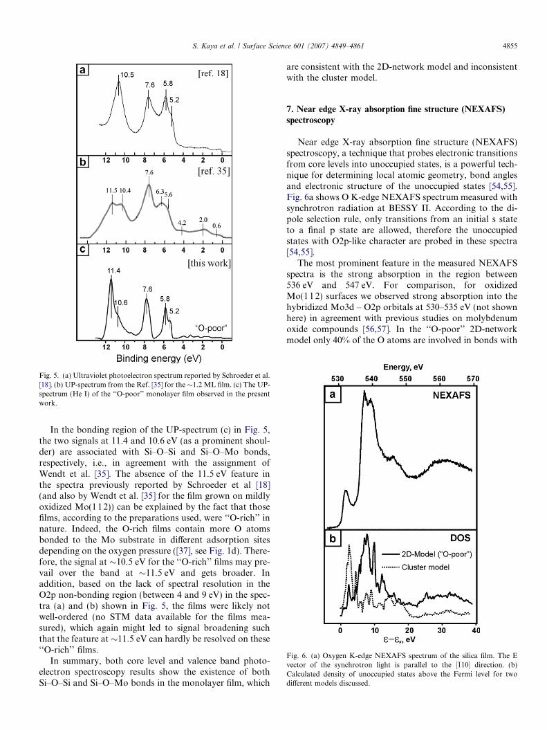
Fig. 5. (a) Ultraviolet photoelectron spectrum reported by Schroeder et al.[18]. (b) UP-spectrum from the Ref. [35] for the �1.2 ML film. (c) The UP-spectrum (He I) of the ‘‘O-poor’’ monolayer film observed in the presentwork.
Fig. 6. (a) Oxygen K-edge NEXAFS spectrum of the silica film. The Evector of the synchrotron light is parallel to the ½�110� direction. (b)Calculated density of unoccupied states above the Fermi level for twodifferent models discussed.
S. Kaya et al. / Surface Science 601 (2007) 4849–4861 4855
In the bonding region of the UP-spectrum (c) in Fig. 5,the two signals at 11.4 and 10.6 eV (as a prominent shoul-der) are associated with Si–O–Si and Si–O–Mo bonds,respectively, i.e., in agreement with the assignment ofWendt et al. [35]. The absence of the 11.5 eV feature inthe spectra previously reported by Schroeder et al [18](and also by Wendt et al. [35] for the film grown on mildlyoxidized Mo(112)) can be explained by the fact that thosefilms, according to the preparations used, were ‘‘O-rich’’ innature. Indeed, the O-rich films contain more O atomsbonded to the Mo substrate in different adsorption sitesdepending on the oxygen pressure ([37], see Fig. 1d). There-fore, the signal at �10.5 eV for the ‘‘O-rich’’ films may pre-vail over the band at �11.5 eV and gets broader. Inaddition, based on the lack of spectral resolution in theO2p non-bonding region (between 4 and 9 eV) in the spec-tra (a) and (b) shown in Fig. 5, the films were likely notwell-ordered (no STM data available for the films mea-sured), which again might led to signal broadening suchthat the feature at �11.5 eV can hardly be resolved on these‘‘O-rich’’ films.
In summary, both core level and valence band photo-electron spectroscopy results show the existence of bothSi–O–Si and Si–O–Mo bonds in the monolayer film, which
are consistent with the 2D-network model and inconsistentwith the cluster model.
7. Near edge X-ray absorption fine structure (NEXAFS)spectroscopy
Near edge X-ray absorption fine structure (NEXAFS)spectroscopy, a technique that probes electronic transitionsfrom core levels into unoccupied states, is a powerful tech-nique for determining local atomic geometry, bond anglesand electronic structure of the unoccupied states [54,55].Fig. 6a shows O K-edge NEXAFS spectrum measured withsynchrotron radiation at BESSY II. According to the di-pole selection rule, only transitions from an initial s stateto a final p state are allowed, therefore the unoccupiedstates with O2p-like character are probed in these spectra[54,55].
The most prominent feature in the measured NEXAFSspectra is the strong absorption in the region between536 eV and 547 eV. For comparison, for oxidizedMo(112) surfaces we observed strong absorption into thehybridized Mo3d – O2p orbitals at 530–535 eV (not shownhere) in agreement with previous studies on molybdenumoxide compounds [56,57]. In the ‘‘O-poor’’ 2D-networkmodel only 40% of the O atoms are involved in bonds with
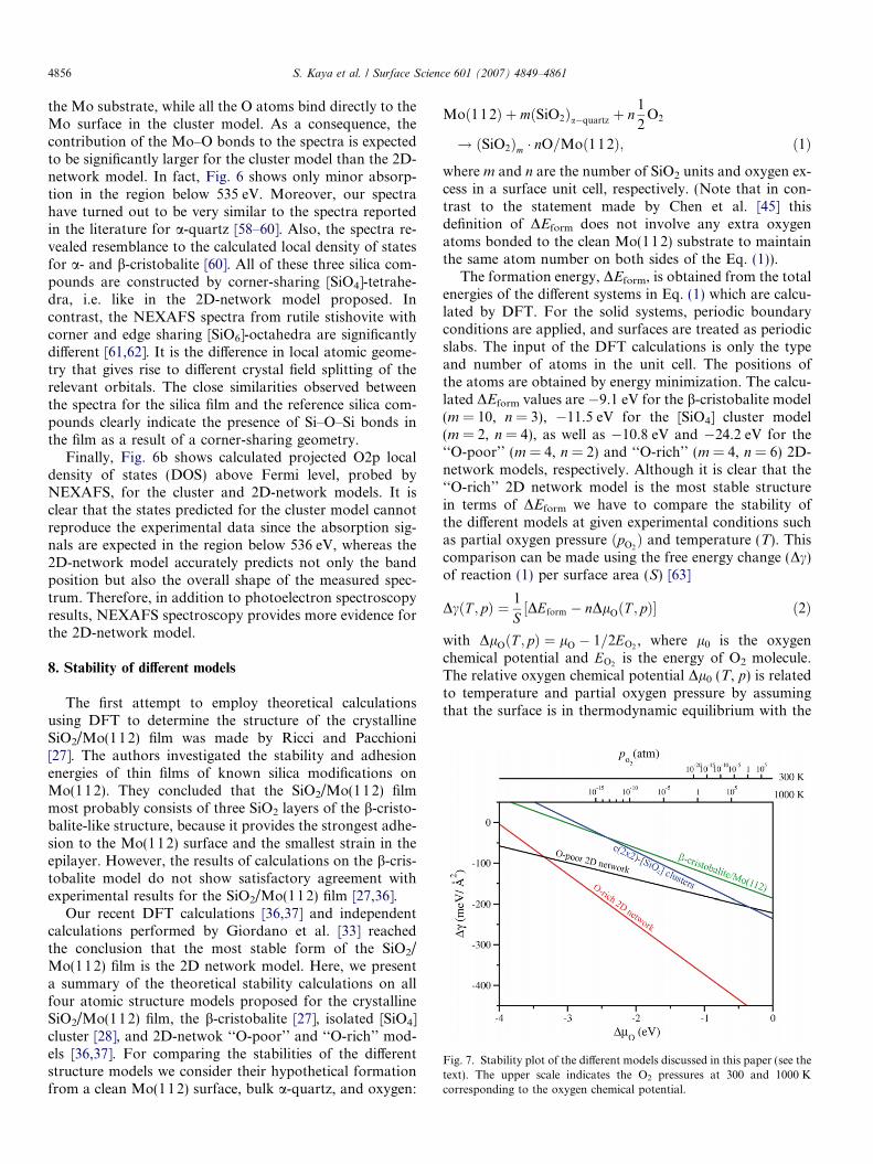
Fig. 7. Stability plot of the different models discussed in this paper (see thetext). The upper scale indicates the O2 pressures at 300 and 1000 Kcorresponding to the oxygen chemical potential.
4856 S. Kaya et al. / Surface Science 601 (2007) 4849–4861
the Mo substrate, while all the O atoms bind directly to theMo surface in the cluster model. As a consequence, thecontribution of the Mo–O bonds to the spectra is expectedto be significantly larger for the cluster model than the 2D-network model. In fact, Fig. 6 shows only minor absorp-tion in the region below 535 eV. Moreover, our spectrahave turned out to be very similar to the spectra reportedin the literature for a-quartz [58–60]. Also, the spectra re-vealed resemblance to the calculated local density of statesfor a- and b-cristobalite [60]. All of these three silica com-pounds are constructed by corner-sharing [SiO4]-tetrahe-dra, i.e. like in the 2D-network model proposed. Incontrast, the NEXAFS spectra from rutile stishovite withcorner and edge sharing [SiO6]-octahedra are significantlydifferent [61,62]. It is the difference in local atomic geome-try that gives rise to different crystal field splitting of therelevant orbitals. The close similarities observed betweenthe spectra for the silica film and the reference silica com-pounds clearly indicate the presence of Si–O–Si bonds inthe film as a result of a corner-sharing geometry.
Finally, Fig. 6b shows calculated projected O2p localdensity of states (DOS) above Fermi level, probed byNEXAFS, for the cluster and 2D-network models. It isclear that the states predicted for the cluster model cannotreproduce the experimental data since the absorption sig-nals are expected in the region below 536 eV, whereas the2D-network model accurately predicts not only the bandposition but also the overall shape of the measured spec-trum. Therefore, in addition to photoelectron spectroscopyresults, NEXAFS spectroscopy provides more evidence forthe 2D-network model.
8. Stability of different models
The first attempt to employ theoretical calculationsusing DFT to determine the structure of the crystallineSiO2/Mo(112) film was made by Ricci and Pacchioni[27]. The authors investigated the stability and adhesionenergies of thin films of known silica modifications onMo(112). They concluded that the SiO2/Mo(112) filmmost probably consists of three SiO2 layers of the b-cristo-balite-like structure, because it provides the strongest adhe-sion to the Mo(112) surface and the smallest strain in theepilayer. However, the results of calculations on the b-cris-tobalite model do not show satisfactory agreement withexperimental results for the SiO2/Mo(11 2) film [27,36].
Our recent DFT calculations [36,37] and independentcalculations performed by Giordano et al. [33] reachedthe conclusion that the most stable form of the SiO2/Mo(112) film is the 2D network model. Here, we presenta summary of the theoretical stability calculations on allfour atomic structure models proposed for the crystallineSiO2/Mo(112) film, the b-cristobalite [27], isolated [SiO4]cluster [28], and 2D-netwok ‘‘O-poor’’ and ‘‘O-rich’’ mod-els [36,37]. For comparing the stabilities of the differentstructure models we consider their hypothetical formationfrom a clean Mo(112) surface, bulk a-quartz, and oxygen:
Moð112Þ þ mðSiO2Þa�quartz þ n1
2O2
! ðSiO2Þm � nO=Moð1 12Þ; ð1Þ
where m and n are the number of SiO2 units and oxygen ex-cess in a surface unit cell, respectively. (Note that in con-trast to the statement made by Chen et al. [45] thisdefinition of DEform does not involve any extra oxygenatoms bonded to the clean Mo(11 2) substrate to maintainthe same atom number on both sides of the Eq. (1)).
The formation energy, DEform, is obtained from the totalenergies of the different systems in Eq. (1) which are calcu-lated by DFT. For the solid systems, periodic boundaryconditions are applied, and surfaces are treated as periodicslabs. The input of the DFT calculations is only the typeand number of atoms in the unit cell. The positions ofthe atoms are obtained by energy minimization. The calcu-lated DEform values are �9.1 eV for the b-cristobalite model(m = 10, n = 3), �11.5 eV for the [SiO4] cluster model(m = 2, n = 4), as well as �10.8 eV and �24.2 eV for the‘‘O-poor’’ (m = 4, n = 2) and ‘‘O-rich’’ (m = 4, n = 6) 2D-network models, respectively. Although it is clear that the‘‘O-rich’’ 2D network model is the most stable structurein terms of DEform we have to compare the stability ofthe different models at given experimental conditions suchas partial oxygen pressure ðpO2
Þ and temperature (T). Thiscomparison can be made using the free energy change (Dc)of reaction (1) per surface area (S) [63]
DcðT ; pÞ ¼ 1
S½DEform � nDlOðT ; pÞ� ð2Þ
with DlOðT ; pÞ ¼ lO � 1=2EO2, where l0 is the oxygen
chemical potential and EO2is the energy of O2 molecule.
The relative oxygen chemical potential Dl0 (T, p) is relatedto temperature and partial oxygen pressure by assumingthat the surface is in thermodynamic equilibrium with the
S. Kaya et al. / Surface Science 601 (2007) 4849–4861 4857
gas phase O2 [63]. The stability plot of Dc (T, p) for the se-lected models is presented in Fig. 7, which clearly showsthat the 2D-network models are the most stable systemsat any experimentally relevant conditions. Note, that theexistence of the ‘‘O-rich’’ phase of the 2D film has not beenexplicitly considered by Chen and Goodman in their recentpublications [43,45], particularly concerning qualitativeanalysis of the stability of different silica film models.
9. Vibrational spectroscopy: experiment vs. theory
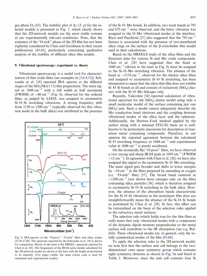
Vibrational spectroscopy is a useful tool for character-ization of thin oxide films (see examples in [3,6,9,12]). Sch-roeder et al. [18] reported IRA spectra at the differentstages of the SiO2/Mo(112) film preparation. The main sig-nal at 1048 cm�1 with a full width at half maximum(FWHM) of �40 cm�1 (Fig. 8), observed for the orderedfilms, as judged by LEED, was assigned to asymmetricSi–O–Si stretching vibrations. A strong frequency shiftfrom 1150 to 1200 cm�1 (typically observed for this vibra-tion mode in the bulk silica) was attributed to the presence
Fig. 8. IRA-spectra of the ‘‘O-poor’’, ‘‘O-rich’’ films and silica stripes[33,36,37,40]. The spectrum reported by the Schroeder et al. [18] is shownfor comparison. Shown in the inset is the HREEL- spectrum reported byChen et al. [28]. The frequencies of the IRAS active modes calculated forthe 2D-network model are shown as the bars with the height proportionalto its intensity. (For paper online: the same colour code is used forcalculated and experimental results).
of the Si–O–Mo bonds. In addition, two weak bands at 795and 675 cm�1 were observed, and the latter vibration wasassigned to the O–Mo vibrational modes at the interface.Ricci and Pacchioni [27] also suggested that the 795 cm�1
feature is associated with the presence of two-memberedsilica rings on the surface of the b-cristobalite film modelused in their calculations.
Based on the HREELS study of the silica films and theliterature data for various Si and Mo oxide compounds,Chen et al. [28] have suggested that the band at1048 cm�1 (shown in the inset in Fig. 8) must be assignedto the Si–O–Mo stretching vibration. The absence of theband at �1176 cm�1, observed for the thicker silica filmsand assigned to asymmetric Si–O–Si stretching, has beeninterpreted to mean that the ultra-thin film does not exhibitSi–O–Si bonds at all and consists of exclusively [SiO4] clus-ters with the Si–O–Mo linkages only.
Recently, Yakovkin [34] reported calculation of vibra-tional spectrum for the [SiO4] cluster model using only asmall molecular model of the surface containing just one[SiO4] unit. Such a model cannot adequately describe theMo conduction band electrons and the coupling betweenvibrational modes of the silica layer and the substrate.Additionally, the Hartree–Fock method applied by theauthor along with a minimal STO-3G basis set is well-known to be particularly inaccurate for description of tran-sition metal containing compounds. Therefore, in ouropinion the reported agreement between the calculatedSi–O stretching frequency at 1044 cm�1 and experimentalvalue at 1048 cm�1 is purely accidental.
On the atomically flat ‘‘O-poor’’ films, we have observeda very strong and sharp IRAS peak at 1059 cm�1 (FWHM�12 cm�1). In agreement with Chen et al. [28], we have alsoassigned this signal to the asymmetric Si–O–Mo stretching.The main signal gets broader and shifts to lower energiesby �10 cm�1 in the films prepared by annealing in oxygen(i.e. ‘‘O-rich’’ film) [37]. The broad band centered at�1200 cm�1 (not shown here) emerges only on the filmscontaining silica particles [36], which is therefore assignedto asymmetric Si–O–Si stretching in the bulk silica. How-ever, the absence of the absorption bands characteristicfor the Si–O–Si vibrations in the monolayer film does notstraightforwardly mean the absence of the Si–O–Si bondsas postulated by Chen et al. [28]. In fact, this effect canbe rationalized on the basis of the selection rules appliedto the refractory metal surfaces.
The selection rule (which holds true for the thin films aswell) states that only vibrational modes with a componentof the dynamic dipole moment perpendicular to the metalsurface will contribute to the IR absorption (see e.g. Ref.[64]). These vibrational modes are, in general, only the to-tally symmetrical modes of the film [65,66].
To apply the selection rules to the 2D-network model,we note first that the surface unit cell belongs to the two-dimensional cmm space symmetry group which containseight symmetry elements as shown in Fig. 9a and listed inTable 1. Moreover, since the unit cell contains four Si
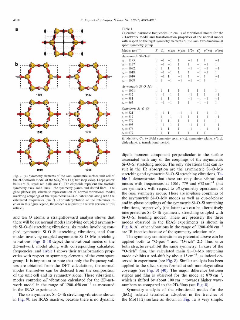
Fig. 9. (a) Symmetry elements of the cmm symmetric surface unit cell ofthe 2D-network model of the SiO2/Mo(112) film (top view). Large yellowballs are Si, small red balls are O. The ellipsoids represent the twofoldsymmetry axes, solid lines – the symmetry planes and dotted lines – theglide planes; (b) schematic representation of normal vibrational modesinvolving couplings of the asymmetric Si–O–Si vibrations along with thecalculated frequencies (cm�1). (For interpretation of the references tocolor in this figure legend, the reader is referred to the web version of thisarticle.)
Table 1Calculated harmonic frequencies (in cm�1) of vibrational modes for the2D-network model and transformation properties of the normal modeswith respect to the eight symmetry elements of the cmm two-dimensionalspace symmetry group
Modes (cm�1) E C2 r(xz) r(yz) 1/2s C02 r 0(xz) r 0(yz)
Asymmetric Si–O–Si
v1 = 1195 1 �1 �1 1 �1 1 1 �1v2 = 1137 1 �1 �1 1 1 �1 �1 1v3 = 1092 1 1 1 1 �1 �1 �1 �1v4 = 1018 1 �1 �1 1 1 �1 �1 1v5 = 1010 1 �1 1 �1 1 �1 1 �1v6 = 1008 1 1 �1 �1 �1 �1 1 1
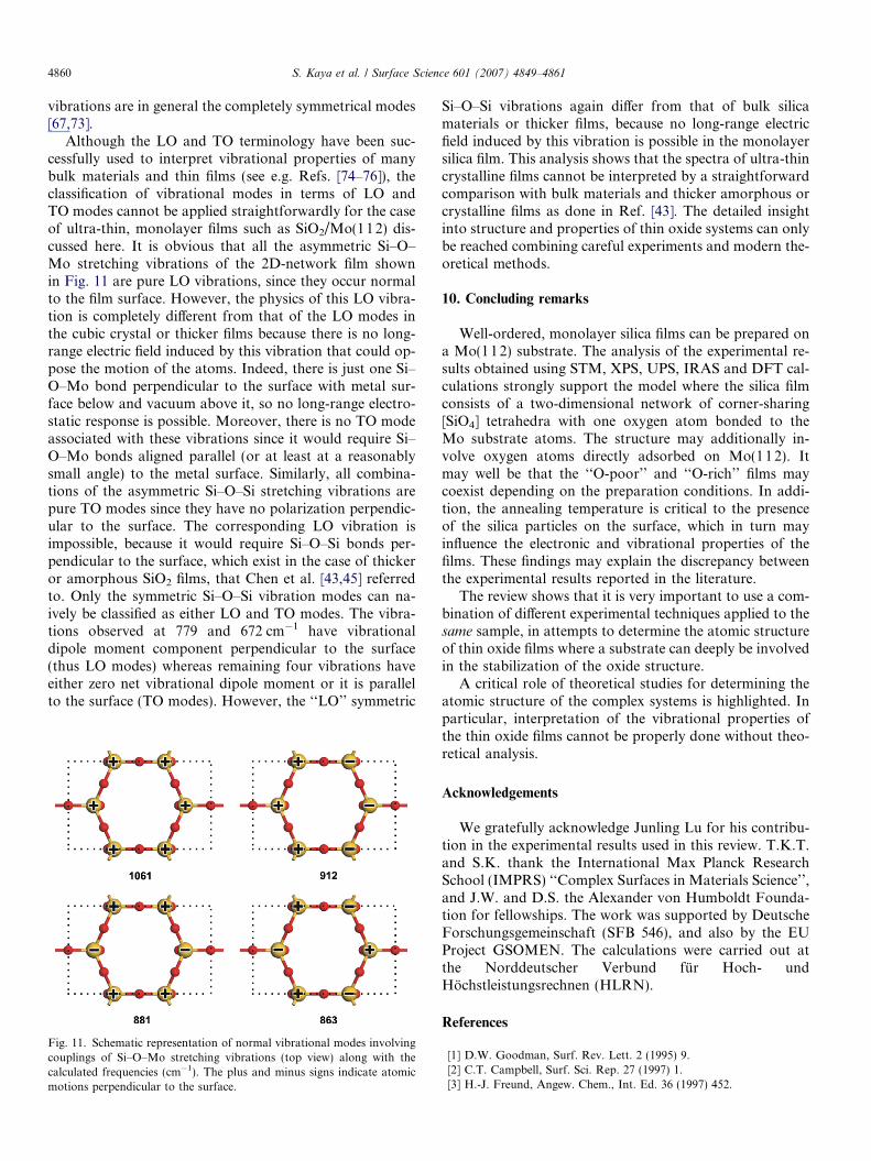
Asymmetric Si–O–Mo
v1 = 1061 1 1 1 1 1 1 1 1v2 = 912 1 �1 �1 1 �1 1 1 �1v3 = 881 1 1 1 1 �1 �1 �1 �1v4 = 863 1 �1 �1 1 1 �1 �1 1
Symmetric Si–O–Si
v1 = 821 1 �1 1 �1 �1 1 �1 1v2 = 817 1 1 �1 �1 1 1 �1 �1v3 = 779 1 1 1 1 1 1 1 1v4 = 695 1 �1 �1 1 �1 1 1 �1v5 = 676 1 1 1 1 �1 �1 �1 �1v6 = 672 1 1 1 1 1 1 1 1
E: identity; C2: twofold symmetry axis; r(xz): symmetry plane; r0(xz):glide plane; s: translational period.
4858 S. Kaya et al. / Surface Science 601 (2007) 4849–4861
and ten O atoms, a straightforward analysis shows thatthere will be six normal modes involving coupled asymmet-ric Si–O–Si stretching vibrations, six modes involving cou-pled symmetric Si–O–Si stretching vibrations, and fourmodes involving coupled asymmetric Si–O–Mo stretchingvibrations. Figs. 8–10 depict the vibrational modes of the2D-network model along with corresponding calculatedfrequencies, and Table 1 shows their transformation prop-erties with respect to symmetry elements of the cmm spacegroup. It is important to note that only the frequency val-ues are obtained from the DFT calculations, the normalmodes themselves can be deduced from the compositionof the unit cell and its symmetry alone. These vibrationalmodes comprise all vibrations calculated for the 2D-net-work model in the range of 1200–650 cm�1 as measuredin the IRAS experiments.
The six asymmetric Si–O–Si stretching vibrations shownin Fig. 9b are IRAS inactive, because there is no dynamic
dipole moment component perpendicular to the surfaceassociated with any of the couplings of the asymmetricSi–O–Si stretching modes. The only vibrations that can re-sult in the IR absorption are the asymmetric Si–O–Mostretching and symmetric Si–O–Si stretching vibrations. Ta-ble 1 demonstrates that there are only three vibrationalmodes with frequencies at 1061, 779 and 672 cm�1 thatare symmetric with respect to all symmetry operations ofthe cmm symmetry group. These are in-phase couplings ofthe asymmetric Si–O–Mo modes as well as out-of-phaseand in-phase couplings of the symmetric Si–O–Si stretchingvibrations, respectively (the latter two can be alternativelyinterpreted as Si–O–Si symmetric stretching coupled withSi–O–Si bending modes). These are precisely the threemodes observed in the IRAS experiments as shown inFig. 8. All other vibrations in the range of 1200–650 cm�1
are IR inactive because of the symmetry selection rule.The symmetry considerations as presented above can be
applied both to ‘‘O-poor’’ and ‘‘O-rich’’ 2D films sinceboth structures exhibit the same symmetry. In case of the‘‘O-rich’’ film, the calculated main Si–O–Mo stretchingmode exhibits a red-shift by about 15 cm�1, as indeed ob-served in experiment (see Fig. 8). Similar analysis has beenapplied to the silica stripes formed at sub-monolayer silicacoverage (see Fig. 3) [40]. The major difference betweenstripes and film is observed for the mode at 879 cm�1,which is shifted by about 100 cm�1 towards higher wave-numbers as compared to the 2D-films (see Fig. 8).
Symmetry analysis of the vibrational modes for the[SiO4] isolated tetrahedra adsorbed in the trenches ofthe Mo(11 2) surface as shown in Fig. 1a is very simple.
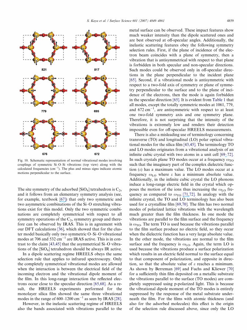
Fig. 10. Schematic representation of normal vibrational modes involvingcouplings of symmetric Si–O–Si vibrations (top view) along with thecalculated frequencies (cm�1). The plus and minus signs indicate atomicmotions perpendicular to the surface.
S. Kaya et al. / Surface Science 601 (2007) 4849–4861 4859
The site symmetry of the adsorbed [SiO4] tetrahedron is C2v
and it follows from an elementary symmetry analysis (see,for example, textbook [67]) that only two symmetric andtwo asymmetric combinations of the Si–O stretching vibra-tions exist for this model. Only the two symmetric combi-nations are completely symmetrical with respect to allsymmetry operations of the C2v symmetry group and there-fore can be observed by IRAS. This is in agreement withour DFT calculations [36], which showed that for the clus-ter model basically only two symmetric O–Si–O vibrationalmodes at 706 and 532 cm�1 are IRAS active. This is in con-trast to the claim [43,45] that the asymmetrical Si–O vibra-tions of the [SiO4] tetrahedron should be always IR active.
In a dipole scattering regime HREELS obeys the sameselection rule that applies to infrared spectroscopy. Onlythe completely symmetrical vibrational modes are allowedwhen the interaction is between the electrical field of theincoming electron and the vibrational dipole moment ofthe film. In this long-range interaction the reflected elec-trons occur close to the specular direction [65,68]. As a re-sult, the HREELS experiments performed for themonolayer silica film showed the same three vibrationalmodes in the range of 600–1200 cm�1 as seen by IRAS [28].
However, in the inelastic scattering regime of HREELSalso the bands associated with vibrations parallel to the
metal surface can be observed. These impact features showmuch weaker intensity than the dipole scattered ones andare best observed at off-specular angles. Additionally, theinelastic scattering features obey the following symmetryselection rules. First, if the plane of incidence of the elec-tron beam coincides with a plane of symmetry, then avibration that is antisymmetrical with respect to that planeis forbidden in both specular and non-specular directions.Such modes could be observed only in off-specular direc-tions in the plane perpendicular to the incident plane[65]. Second, if a vibrational mode is antisymmetric withrespect to a two-fold axis of symmetry or plane of symme-try perpendicular to the surface and to the plane of inci-dence of the electrons, then the mode is again forbiddenin the specular direction [65]. It is evident from Table 1 thatall modes, except the totally symmetric modes at 1061, 779,and 672 cm�1, are antisymmetric with respect to at leastone two-fold symmetry axis and one symmetry plane.Therefore, it is not surprising that the intensity of thevibrations is extremely low and renders their detectionimpossible even for off-specular HREELS measurements.
There is also a misleading use of terminology concerningtransverse (TO) and longitudinal (LO) polar optical vibra-tional modes for the silica film [43,45]. The terminology TOand LO modes originates from a vibrational analysis of aninfinite cubic crystal with two atoms in a unit cell [69–72].In such crystals plane TO modes occur at a frequency xTO
such that the imaginary part of the complex dielectric func-tion (e) has a maximum value. The LO modes occur at afrequency xLO where e has a minimum absolute value.Additionally, in the infinite cubic crystal the LO phononsinduce a long-range electric field in the crystal which op-poses the motion of the ions thus increasing the xLO fre-quency as compared to xTO [71,72]. In analogy with theinfinite crystal, the TO and LO terminology has also beenused for a crystalline film [69,70]. The film has two normalmodes of polarized lattice vibrations with the wavelengthmuch greater than the film thickness. In one mode thevibrations are parallel to the film surface and the frequencyis xTO. The term TO is used because the vibrations parallelto the film surface produce no electric field, so they occurwhen the dielectric function has a very large absolute value.In the other mode, the vibrations are normal to the filmsurface and the frequency is xLO. Again, the term LO isused because the vibrations produce a surface polarizationwhich results in an electric field normal to the surface equalto that component of polarization, and opposite in direc-tion, so that the absolute value of e reaches a minimum.As shown by Berreman [69] and Fuchs and Kliewer [70]for a sufficiently thin film deposited on a metallic substratethe vibrations parallel to the surface (TO modes) are com-pletely suppressed using p-polarized light. This is becausethe vibrational dipole moment of the TO modes is entirelysuppressed by the response of the metal substrate under-neath the film. For the films with atomic thickness (andalso for the adsorbed molecules) this effect is the originof the selection rule discussed above, since only the LO
4860 S. Kaya et al. / Surface Science 601 (2007) 4849–4861
vibrations are in general the completely symmetrical modes[67,73].
Although the LO and TO terminology have been suc-cessfully used to interpret vibrational properties of manybulk materials and thin films (see e.g. Refs. [74–76]), theclassification of vibrational modes in terms of LO andTO modes cannot be applied straightforwardly for the caseof ultra-thin, monolayer films such as SiO2/Mo(112) dis-cussed here. It is obvious that all the asymmetric Si–O–Mo stretching vibrations of the 2D-network film shownin Fig. 11 are pure LO vibrations, since they occur normalto the film surface. However, the physics of this LO vibra-tion is completely different from that of the LO modes inthe cubic crystal or thicker films because there is no long-range electric field induced by this vibration that could op-pose the motion of the atoms. Indeed, there is just one Si–O–Mo bond perpendicular to the surface with metal sur-face below and vacuum above it, so no long-range electro-static response is possible. Moreover, there is no TO modeassociated with these vibrations since it would require Si–O–Mo bonds aligned parallel (or at least at a reasonablysmall angle) to the metal surface. Similarly, all combina-tions of the asymmetric Si–O–Si stretching vibrations arepure TO modes since they have no polarization perpendic-ular to the surface. The corresponding LO vibration isimpossible, because it would require Si–O–Si bonds per-pendicular to the surface, which exist in the case of thickeror amorphous SiO2 films, that Chen et al. [43,45] referredto. Only the symmetric Si–O–Si vibration modes can na-ively be classified as either LO and TO modes. The vibra-tions observed at 779 and 672 cm�1 have vibrationaldipole moment component perpendicular to the surface(thus LO modes) whereas remaining four vibrations haveeither zero net vibrational dipole moment or it is parallelto the surface (TO modes). However, the ‘‘LO’’ symmetric
Fig. 11. Schematic representation of normal vibrational modes involvingcouplings of Si–O–Mo stretching vibrations (top view) along with thecalculated frequencies (cm�1). The plus and minus signs indicate atomicmotions perpendicular to the surface.
Si–O–Si vibrations again differ from that of bulk silicamaterials or thicker films, because no long-range electricfield induced by this vibration is possible in the monolayersilica film. This analysis shows that the spectra of ultra-thincrystalline films cannot be interpreted by a straightforwardcomparison with bulk materials and thicker amorphous orcrystalline films as done in Ref. [43]. The detailed insightinto structure and properties of thin oxide systems can onlybe reached combining careful experiments and modern the-oretical methods.
10. Concluding remarks
Well-ordered, monolayer silica films can be prepared ona Mo(112) substrate. The analysis of the experimental re-sults obtained using STM, XPS, UPS, IRAS and DFT cal-culations strongly support the model where the silica filmconsists of a two-dimensional network of corner-sharing[SiO4] tetrahedra with one oxygen atom bonded to theMo substrate atoms. The structure may additionally in-volve oxygen atoms directly adsorbed on Mo(11 2). Itmay well be that the ‘‘O-poor’’ and ‘‘O-rich’’ films maycoexist depending on the preparation conditions. In addi-tion, the annealing temperature is critical to the presenceof the silica particles on the surface, which in turn mayinfluence the electronic and vibrational properties of thefilms. These findings may explain the discrepancy betweenthe experimental results reported in the literature.
The review shows that it is very important to use a com-bination of different experimental techniques applied to thesame sample, in attempts to determine the atomic structureof thin oxide films where a substrate can deeply be involvedin the stabilization of the oxide structure.
A critical role of theoretical studies for determining theatomic structure of the complex systems is highlighted. Inparticular, interpretation of the vibrational properties ofthe thin oxide films cannot be properly done without theo-retical analysis.
Acknowledgements
We gratefully acknowledge Junling Lu for his contribu-tion in the experimental results used in this review. T.K.T.and S.K. thank the International Max Planck ResearchSchool (IMPRS) ‘‘Complex Surfaces in Materials Science’’,and J.W. and D.S. the Alexander von Humboldt Founda-tion for fellowships. The work was supported by DeutscheForschungsgemeinschaft (SFB 546), and also by the EUProject GSOMEN. The calculations were carried out atthe Norddeutscher Verbund fur Hoch- undHochstleistungsrechnen (HLRN).
References
[1] D.W. Goodman, Surf. Rev. Lett. 2 (1995) 9.[2] C.T. Campbell, Surf. Sci. Rep. 27 (1997) 1.[3] H.-J. Freund, Angew. Chem., Int. Ed. 36 (1997) 452.
S. Kaya et al. / Surface Science 601 (2007) 4849–4861 4861
[4] R. Franchy, Surf. Sci. Rep. 38 (2000) 195.[5] S.A. Chambers, Surf. Sci. Rep. 39 (2000) 105.[6] M. Baumer, H.-J. Freund, Prog. Surf. Sci. 61 (1999) 127.[7] W. Weiss, W. Ranke, Prog. Surf. Sci. 70 (2002) 1.[8] U. Diebold, Surf. Sci. Rep. 48 (2003) 53.[9] G. Kresse, M. Schmid, E. Napetschnig, M. Shishkin, L. Kohler, P.
Varga, Science 308 (2005) 1440.[10] M. Sterrer, M. Yulikov, E. Fischbach, M. Heyde, H.-P. Rust, G.
Pacchioni, T. Risse, H.-J. Freund, Angew. Chem., Int. Ed. 45 (2006)2630.
[11] D.R. Mullins, P.V. Radulovic, S.H. Overbury, Surf. Sci. 429 (1999)186.
[12] J. Schoiswohl, M. Sock, S. Surnev, M.G. Ramsey, F.P. Netzer, G.Kresse, J.N. Andersen, Surf. Sci. 555 (2004) 101.
[13] J.W. He, X. Xu, J.S. Corneille, D.W. Goodman, Surf. Sci. 279 (1992)119.
[14] X. Xu, D.W. Goodman, Surf. Sci. 282 (1993) 323.[15] T. Schroeder, M. Adelt, B. Richter, M. Naschitzki, M. Baumer, H.-J.
Freund, Surf. Rev. Lett. 7 (2000) 7.[16] T. Schroeder, M. Adelt, B. Richter, M. Naschitzki, M. Baumer, H.-J.
Freund, Microelectr. Rel. 40 (2000) 841.[17] T. Schroeder, A. Hammoudeh, M. Pykavy, N. Magg, M. Adelt, M.
Baumer, H.-J. Freund, Solid State Electron. 45 (2001) 1471.[18] T. Schroeder, J.B. Giorgi, M. Baumer, H.-J. Freund, Phys. Rev. B 66
(2002) 165422.[19] J.B. Giorgi, T. Schroeder, M. Baumer, H.-J. Freund, Surf. Sci. 498
(2002) L71.[20] A.K. Santra, B.K. Min, D.W. Goodman, Surf. Sci. 515 (2002) L475.[21] B.K. Min, A.K. Santra, D.W. Goodman, J. Vac. Sci. Technol. B 21
(2003) 2319.[22] Y.D. Kim, T. Wei, D.W. Goodman, Langmuir 19 (2003) 354.[23] B.K. Min, A.K. Santra, D.W. Goodman, Catal. Today 85 (2003) 113.[24] Y.D. Kim, T. Wei, J. Stulz, D.W. Goodman, Langmuir 19 (2003)
1140.[25] E. Ozensoy, B.K. Min, A.K. Santra, D.W. Goodman, J. Phys. Chem.
B 108 (2004) 4351.[26] S. Wendt, M. Frerichs, T. Wei, M. Chen, V. Kempter, D.W.
Goodman, Surf. Sci. 565 (2004) 107.[27] D. Ricci, G. Pacchioni, Phys. Rev. B 69 (2004) 161307.[28] M. Chen, A.K. Santra, D.W. Goodman, Phys. Rev. B 69 (2004)
155404.[29] B.K. Min, W.T. Wallace, D.W. Goodman, J. Phys. Chem. B 108
(2004) 14609.[30] B.K. Min, W.T. Wallace, A.K. Santra, D.W. Goodman, J. Phys.
Chem. B. 108 (2004) 16339.[31] W.T. Wallace, B.K. Min, D.W. Goodman, J. Mol. Catal. A 228
(2005) 3.[32] J. Weissenrieder, S. Kaya, J.-L. Lu, H.-J. Gao, S. Shaikhutdinov, H.-
J. Freund, M.M. Sierka, T.K. Todorova, J. Sauer, Phys. Rev. Lett. 95(2005) 076103.
[33] L. Giordano, D. Ricci, G. Pacchioni, P. Ugliengo, Surf. Sci. 584(2005) 225.
[34] I.N. Yakovkin, Surf. Rev. Lett. 12 (2005) 449.[35] S. Wendt, E. Ozensoy, T. Wei, M. Frerichsr, Y. Cai, M. Chen, D.W.
Goodman, Phys. Rev. B 72 (2005) 115409.[36] T.K. Todorova, M. Sierka, J. Sauer, S. Kaya, J. Weissenrieder, J.-L.
Lu, H.-J. Gao, S. Shaikhutdinov, H.-J. Freund, Phys. Rev. B 73(2006) 165414.
[37] M. Sierka, T.K. Todorova, S. Kaya, D. Stacchiola, J. Weissenrieder,J.-L. Lu, H.-J. Gao, S. Shaikhutdinov, H.-J. Freund, J. Sauer, Chem.Phys. Lett. 424 (2006) 115.
[38] B.K. Min, W.T. Wallace, D.W. Goodman, Surf. Sci. 600 (2006) L7.
[39] L. Giordano, A. Del Vitto, G. Pacchioni, J. Chem. Phys. 124 (2006)034701.
[40] J.-L. Lu, S. Kaya, J. Weissenrieder, T.K. Todorova, M. Sierka, J.Sauer, H.-J. Gao, S. Shaikhutdinov, H.-J. Freund, Surf. Sci. 600(2006) L164.
[41] J.-L. Lu, S. Kaya, J. Weissenrieder, H.-J. Gao, S. Shaikhutdinov, H.-J. Freund, Surf. Sci. 600 (2006) L153.
[42] U. Martinez, L. Giordano, G. Pacchioni, J. Chem. Phys. B 110 (2006)17015.
[43] M. Chen, D.W. Goodman, Surf. Sci. 600 (2006) L255.[44] L. Giordano, D. Ricci, G. Pacchioni, P. Ugliendo, Surf. Sci. 601
(2007) 588.[45] M. Chen, D.W. Goodman, Surf. Sci. 601 (2007) 591.[46] S. Shaikhutdinov, M. Ritter, W. Weiss, Phys. Rev. B 62 (2000) 7535.[47] F. Sedona, S. Agnoli, G. Granozzi, J. Phys. Chem. B 110 (2006)
15359.[48] D.E. Starr, F.M.T. Mendes, J. Middeke, R.-P. Blum, H. Niehus, D.
Lahav, S. Guimond, A. Uhl, T. Kluener, M. Schmal, H. Kuhlenbeck,S. Shaikhutdinov, H.-J. Freund, Surf. Sci. 599 (2005) 14.
[49] J.F. Moulder, W.F. Stickle, P.E. Sobol, K.D. Bomben, Handbook ofX-ray Photoelectron Spectroscopy, Perkin–Elmer Corporation, USA,1992.
[50] F.J. Grunthaner, P.J. Grunthaner, R. Vasguez, B. Lewis, J. Maserj-ian, A. Madhukar, J. Vac. Sci. Technol. 16 (1979) 1443.
[51] T. Schroeder, J. Zegenhagen, N. Magg, B. Immaraporn, H.-J.Freund, Surf. Sci. 552 (2004) 85.
[52] T.H. Di Stefano, D.E. Eastman, Phys. Rev. Lett. 27 (1971) 1560.[53] B. Fischer, R.A. Pollak, T.H. Di Stefano, W.D. Grobman, Phys. Rev.
B 15 (1977) 3193.[54] J. Stohr, NEXAFS Spectroscopy, Springer-Verlag, Berlin, 1992.[55] J.G. Chen, Surf. Sci. Rep. 30 (1997) 1.[56] M. Sing, R. Neudert, H. von Lips, M.S. Golden, et al., Phys. Rev. B
60 (1999) 8661.[57] M. Cavalleri, K. Hermann, S. Guimond, Y. Romanyshyn, H.
Kuhlenbeck, H.-J. Freund, Catal. Today 124 (2007) 21.[58] M. Taillefumier, D. Cabaret, A.-M. Flank, F. Mauri, Phys. Rev. B 66
(2002) 195107.[59] L.A.J. Garvie, P. Rez, J.R. Alvarez, P.R. Buseck, A.J. Craven, R.
Brydson, Am. Mineral. 85 (2000) 732.[60] I. Tanaka, J. Kawai, H. Adachi, Phys. Rev. B 52 (1995) 11733.[61] A.V. Soldatov, M. Kasrai, G.M. Bancroft, Solid State Commun. 115
(2000) 687.[62] S.-D. Mo, W.Y. Ching, Appl. Phys. Lett. 78 (2001) 3809.[63] K. Reuter, M. Scheffler, Phys. Rev. B 65 (2002) 035406.[64] F.M. Hoffman, Surf. Sci. Rep. 3 (1983) 107.[65] N. Sheppard, J. Erkelens, Appl. Spectros. 38 (1984) 471.[66] A.M. Bradshaw, N.V. Richardson, Pure Appl. Chem. 68 (1996) 457.[67] H. Ibach, D.L. Mils, Electron Energy Loss Spectroscopy and Surface
Vibrations, Academic Press, New York, 1982.[68] H. Ibach, Surf. Sci. 66 (1977) 56.[69] D.W. Berreman, Phys. Rev. 130 (1963) 2193.[70] R. Fuchs, K.L. Kliewer, Phys. Rev. 140 (1965) 2076.[71] M. Born, K. Huang, Dynamical Theory of Crystal Lattices, Oxford
University Press, Oxford, 1966.[72] H. Bottger, Principles of the Theory of Lattice Dynamics, Physik-
Werlag, Weinheim, 1983.[73] H.A. Pearce, N. Sheppard, Surf. Sci. 59 (1976) 205.[74] F.L. Galeener, G. Lucovsky, Phys. Rev. Lett. 37 (1976) 1474.[75] B. Harbecke, B. Heinz, P. Grosse, Appl. Phys. A 38 (1985) 263.[76] P. Grosse, B. Harbecke, B. Heinz, R. Meyer, M. Offenberg, Appl.
Phys. A 39 (1986) 257.
Related Documents