On-chip quantum interference between silicon photon-pair sources J. W. Silverstone 1 , D. Bonneau 1 , K. Ohira 2 , N. Suzuki 2 , H. Yoshida 2 , N. Iizuka 2 , M. Ezaki 2 , C. M. Natarajan 3 , M. G. Tanner 4 , R. H. Hadfield 4 , V. Zwiller 5 , G. D. Marshall 1 , J. G. Rarity 1 , J. L. O’Brien 1 and M. G. Thompson 1,† 1 Centre for Quantum Photonics, H. H. Wills Physics Laboratory & Department of Electrical and Electronic Engineering, University of Bristol, Merchant Venturers Building, Woodland Road, Bristol BS8 1UB, UK 2 Corporate Research & Development Center, Toshiba Corporation, 1, Komukai Toshiba-cho, Saiwai-ku, Kawasaki 212-8582, Japan 3 E. L. Ginzton Laboratory, Stanford University, Stanford 94305, USA 4 School of Engineering, University of Glasgow, Glasgow G12 8QQ, UK 5 Kavli Institute of Nanoscience, TU Delft, 2628CJ Delft, The Netherlands † Please direct correspondence to: [email protected] Large-scale integrated quantum photonic technologies[1, 2] will require the on-chip integration of identical photon sources with reconfigurable waveguide cir- cuits. Relatively complex quantum circuits have already been demonstrated[3, 4, 5, 6, 7], but few studies acknowledge the pressing need to integrate photon sources and waveguide circuits together on-chip[8, 9]. A key step towards such large-scale quantum technologies is the integration of just two individual pho- ton sources within a waveguide circuit, and the demonstration of high-visibility quantum interference between them. Here, we report a silicon-on-insulator de- vice combining two four-wave mixing sources, in an interferometer with a recon- figurable phase shifter. We configure the device to create and manipulate two- colour (non-degenerate) or same-colour (degenerate), path-entangled or path- unentangled photon pairs. We observe up to 100.0 ± 0.4% visibility quantum interference on-chip, and up to 95 ± 4% off-chip. Our device removes the need for external photon sources, provides a path to increasing the complexity of quantum photonic circuits, and is a first step towards fully-integrated quantum technologies. Most quantum waveguide circuits to date have been fabricated from glass-based materials, which offer low propagation loss, a wide transparency window, and efficient coupling to optical fibre, but also limit device functionality and suffer from large circuit footprints. The silicon-on-insulator photonics platform (SOI), recently developed for classical applications[10, 11], has several advantages over glass-based systems, including a high component density, a strong χ (3) optical nonlinearity, mature fabrication techniques, fast optical modulators[12], and compatibility with both 1550-nm telecom optics and CMOS electronics. As such, SOI quantum photonic circuits [13] and spontaneous photon-pair sources [14, 15, 16, 17, 18] have recently been shown. Our SOI photonic device is presented in Fig. 1a. Inside the device are two photon-pair sources, each comprising a 5.2-mm-long spiraled silicon waveguide in which the χ (3) spontaneous four-wave mixing (SFWM) process is possible (region II, Fig. 1a). SFWM creates a signal- 1

Welcome message from author
This document is posted to help you gain knowledge. Please leave a comment to let me know what you think about it! Share it to your friends and learn new things together.
Transcript
On-chip quantum interference
between silicon photon-pair sources
J. W. Silverstone1, D. Bonneau1, K. Ohira2, N. Suzuki2, H. Yoshida2, N. Iizuka2,M. Ezaki2, C. M. Natarajan3, M. G. Tanner4, R. H. Hadfield4, V. Zwiller5,
G. D. Marshall1, J. G. Rarity1, J. L. O’Brien1 and M. G. Thompson1,†
1Centre for Quantum Photonics, H. H. Wills Physics Laboratory & Department of Electrical andElectronic Engineering, University of Bristol, Merchant Venturers Building, Woodland Road,
Bristol BS8 1UB, UK2Corporate Research & Development Center, Toshiba Corporation, 1, Komukai Toshiba-cho,
Saiwai-ku, Kawasaki 212-8582, Japan3E. L. Ginzton Laboratory, Stanford University, Stanford 94305, USA4School of Engineering, University of Glasgow, Glasgow G12 8QQ, UK
5Kavli Institute of Nanoscience, TU Delft, 2628CJ Delft, The Netherlands†Please direct correspondence to: [email protected]
Large-scale integrated quantum photonic technologies[1, 2] will require theon-chip integration of identical photon sources with reconfigurable waveguide cir-cuits. Relatively complex quantum circuits have already been demonstrated[3,4, 5, 6, 7], but few studies acknowledge the pressing need to integrate photonsources and waveguide circuits together on-chip[8, 9]. A key step towards suchlarge-scale quantum technologies is the integration of just two individual pho-ton sources within a waveguide circuit, and the demonstration of high-visibilityquantum interference between them. Here, we report a silicon-on-insulator de-vice combining two four-wave mixing sources, in an interferometer with a recon-figurable phase shifter. We configure the device to create and manipulate two-colour (non-degenerate) or same-colour (degenerate), path-entangled or path-unentangled photon pairs. We observe up to 100.0± 0.4% visibility quantuminterference on-chip, and up to 95± 4% off-chip. Our device removes the needfor external photon sources, provides a path to increasing the complexity ofquantum photonic circuits, and is a first step towards fully-integrated quantumtechnologies.
Most quantum waveguide circuits to date have been fabricated from glass-based materials,which offer low propagation loss, a wide transparency window, and efficient coupling tooptical fibre, but also limit device functionality and suffer from large circuit footprints. Thesilicon-on-insulator photonics platform (SOI), recently developed for classical applications[10,11], has several advantages over glass-based systems, including a high component density, astrong χ(3) optical nonlinearity, mature fabrication techniques, fast optical modulators[12],and compatibility with both 1550-nm telecom optics and CMOS electronics. As such, SOIquantum photonic circuits [13] and spontaneous photon-pair sources [14, 15, 16, 17, 18] haverecently been shown.
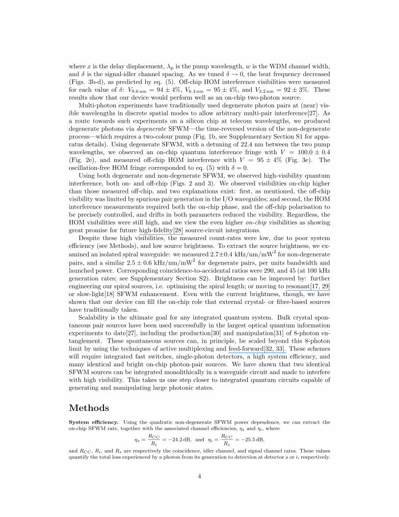
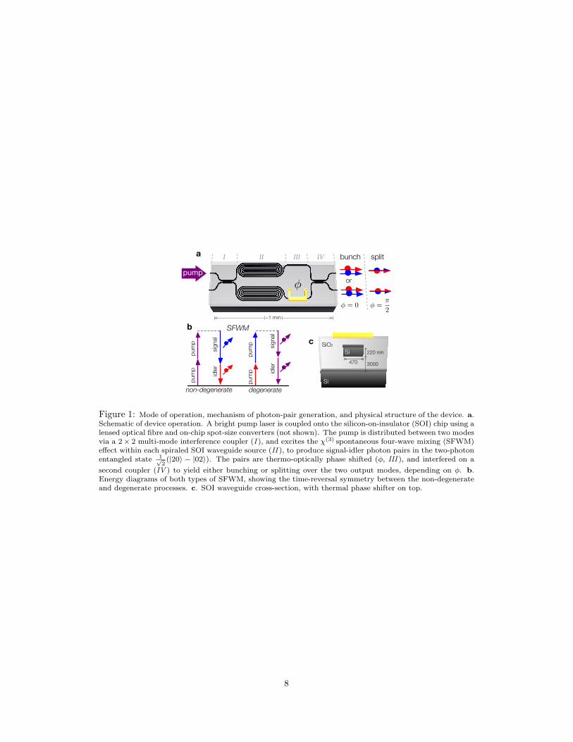
Our SOI photonic device is presented in Fig. 1a. Inside the device are two photon-pairsources, each comprising a 5.2-mm-long spiraled silicon waveguide in which the χ(3) spontaneousfour-wave mixing (SFWM) process is possible (region II, Fig. 1a). SFWM creates a signal-
1
idler photon pair by annihilating two photons from a bright pump beam (Fig. 1b). Non-degenerate pairs are created by a single-wavelength pump, while degenerate pairs require adual-wavelength scheme[19, 20]. In our experiments, two amplified continuous-wave lasersproduced the required pump field. Pump distribution and single-photon interference wereachieved using 2×2 multi-mode interference couplers (MMI, reflectivity ≈ 50%), while a ther-mal phase-shifter modified the on-chip quantum and bright-light states. Off-chip wavelength-division multiplexers (WDM) were used to separate the signal, idler, and pump channels, be-fore the photon pairs were finally measured by two superconducting single-photon detectors(dark count rate 1 kHz, gate width 650 ps).
Evolution of the degenerate quantum and bright-light states proceeded, referring to re-gions (I -IV ) of Fig. 1a, as follows. The bright pump was equally split by the first MMI(I ) between the two sources (II ). By operating in the weak pump regime (so that only onepair was likely to be generated), the simultaneous pumping of both sources yielded a path-entangled N00N state: 1√
2(|20〉 − |02〉). The relative phase was then dynamically controlled
via a thermal phase-shifter in one arm (III ), which applied a φ shift to the bright-light pumpand a 2φ shift to the entangled biphoton state: 1√
2(|20〉 − ei2φ|02〉). Finally, the bright-light
and biphoton states were interfered on a second MMI (IV ) to yield Mach-Zehnder inter-ference fringes in the bright pump transmission, and half-period (λ2 -like) fringes[21] in thephoton pair statistics, of the form
|Ψout〉 = cosφ |Ψbunch〉+ sinφ |Ψsplit〉 . (1)
Here, the |Ψbunch〉 state describes photons bunched together (coalesced) in either output modeA or B, and the |Ψsplit〉 state describes pair splitting, with one photon in each mode[20]. Byconsidering the degenerate pair case, and specifically setting φ = 0 or φ = π
2 , we can obtaineither state at the output:
|Ψout〉 =
{|Ψbunch〉 = 1√
2
(|20〉 − |02〉
), for φ = 0
|Ψsplit〉 = |11〉, for φ = π2 .
(2)
When non-degenerate pairs are created, signal-idler exchange symmetry leads to identicalquantum evolution and non-classical interference as eqs. (1,2). The corresponding |Ψbunch〉and |Ψsplit〉 states for non-degenerate SFWM are:
|Ψbunch〉 =1√2
(|1s1i〉A|0s0i〉B − |0s0i〉A|1s1i〉B
)|Ψsplit〉 =
1√2
(|1s0i〉A|0s1i〉B + |0s1i〉A|1s0i〉B
),
(3)
where s and i indicate signal and idler wavelengths (for more detail, see SupplementarySection S4). We will show experimentally that these non-degenerate colour-entangled[22, 23]states behave like degenerate pairs.
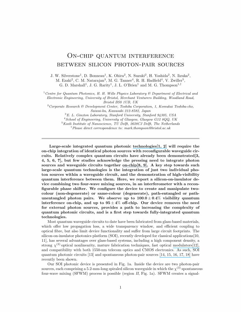
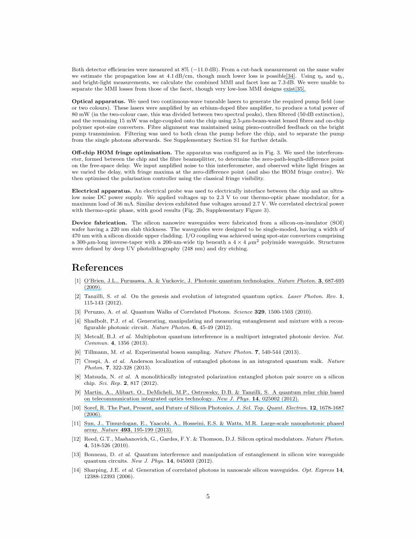
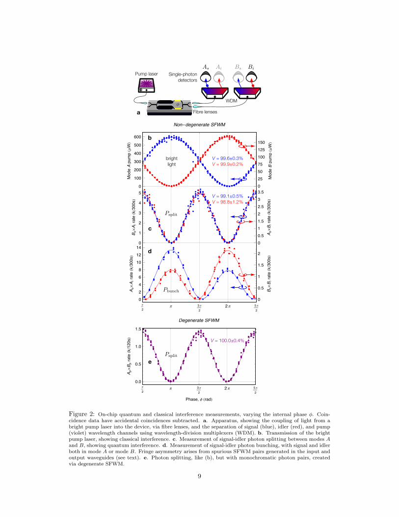
High-visibility quantum interference—the non-classical interference between two photons[24]on a beamsplitter—underpins all of photonic quantum information science and technology.Quantum interference within our device was quantified by the splitting and bunching prob-abilities at the output, Psplit and Pbunch, as the on-chip phase (φ) was varied; classicalinterference was observed in the transmission of the bright pump through the interferometer.First, we manipulated the on-chip path entanglement of the two-colour (non-degenerate)pairs. The experimental apparatus is pictured in Fig. 2a, and detailed in SupplementarySection S1. WDMs separated the monochromatic 1549.6-nm pump from the non-degeneratesignal and idler photons (detuned by δ = 6.4 nm) such that signal-idler coincidences and
2
pump transmission could be measured at the same time. Detector coincidences As×Bi andBs×Ai were measured for Psplit, while As×Ai and Bs×Bi were measured for Pbunch. Therates of classical transmission, as well as Psplit, and Pbunch are recorded in Figs. 2b, 2c,and 2d, respectively. In all cases, high-visibility interference was observed, and both thePsplit and Pbunch two-photon fringes exhibited a phase-doubling compared to their classicalcounterparts—a signature of path-entangled two-photon N00N states.
According to equation (1), the splitting rate should follow Psplit ∝ sin2 φ (curves, Fig. 2c).This model works well, with the data exhibiting net visibilities of 99.1±0.5% for Ai×Bs, and98.8± 1.2% for As×Bi, where we compute the visibility V = (Nmax −Nmin)/Nmax from themaximum Nmax and minimum Nmin values of each fit. The uncorrected visibilities for thesemeasurements remained around 96%—all raw visibilities, including those for the followingmeasurements, are listed in Supplementary Section S7. Meanwhile, for the bunching rate,eq. (1) predicts Pbunch ∝ cos2 φ, but an asymmetric behaviour is observed instead (Fig. 2d).This behaviour can be explained by considering spurious SFWM in the device’s input andoutput (I/O) waveguides—identical in cross-section to the source waveguides (Fig. 1c). Wecalculate corrected bunching probabilities, PAbunch and PBbunch, at the two output modes Aand B as,
PABbunch =
∣∣(Γ0 + ΓI/O) cosφ∓ ΓI/O
∣∣2 (4)
where Γ0 is the base SFWM rate of the spiral sources, and ΓI/O quantifies the generation rateof spurious pairs inside the I/O waveguides (see Supplementary Section S5). Equation (4)describes the Pbunch data well (curves, Fig. 2c). We extracted the spurious pair rate Γ2
I/O,and found that such pairs accounted for a small fraction of the total: Γ2
I/O/Γ20 = 2.5% for
PAbunch, and 2.1% for PBbunch. Since SFWM efficiency scales quadratically with interactionlength (Γ2 ∝ L2, see Supplementary Section S3), we compared these ratios with the I/O-to-source waveguide-length ratio squared, L2
I/O/L20 = 2.0%, and found good agreement. The
Γ2I/O/Γ
20 ratio is of considerable importance—it measures the amount of |Ψbunch〉 contami-
nation when the device is configured to produce only |Ψsplit〉 . In our experiments, spuriouspairs limited the observable off-chip quantum interference visibility to V < 98% (Supple-mentary Section S6). This noise could be suppressed by modifying the waveguide geometryoutside the source regions[15], or by moving to resonant sources[17].
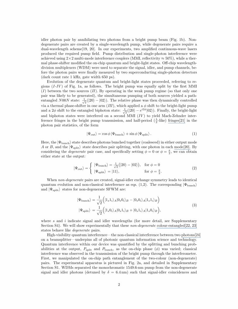
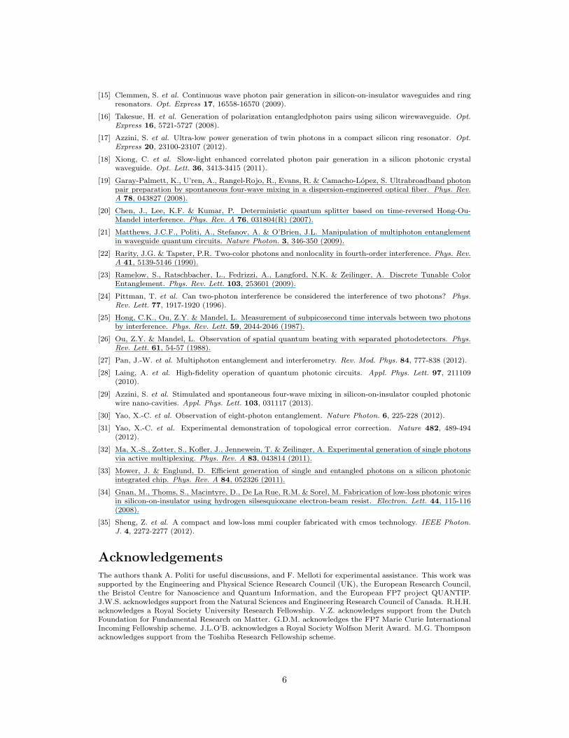
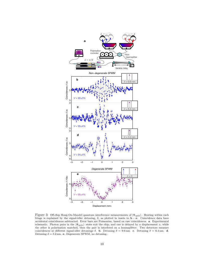
To show how our |Ψsplit〉 pairs could be used in an external circuit, and to explore theimplications of the colour entanglement of our non-degenerate pairs, we performed severaloff-chip Hong-Ou-Mandel-type (HOM) quantum interference measurements[25], for variousvalues of the signal-idler detuning δ. The modified apparatus is pictured in Fig. 3a. Weconfigured the device to generate |Ψsplit〉 at the chip output (by setting φ = π/2), then sentone photon to a tunable delay line, and the other to a polarisation controller. Thus, theoptical path and polarisation of the two photons could be precisely matched, and we couldintroduce distinguishability in the arrival time degree of freedom. The photon pairs theninterfered on a fibre beamsplitter (R = 50.2%), and we recorded coincidences while varyingthe arrival time (via the free-space displacement, x).
The phase-stable two-colour |Ψsplit〉 state yielded HOM interference fringes (Fig. 3b-d)which exhibited a beating between the non-degenerate signal and idler wavelengths[26, 22](with detuning δ). Due to the colour entanglement present in |Ψsplit〉 , the filtered biphotonspectrum has two lobes—one lobe from each of the signal- and idler-channel filters (insetsFig. 3b-d). Since the time-domain HOM interference pattern is effectively the Fourier trans-form of this spectrum, we can calculate the coincidence probability after the beamsplitter tobe
PHOM =12− V
2cos(
2πxδ
λ2p
)sinc
(2πx
w
λ2p
), (5)
3
where x is the delay displacement, λp is the pump wavelength, w is the WDM channel width,and δ is the signal-idler channel spacing. As we tuned δ → 0, the beat frequency decreased(Figs. 3b-d), as predicted by eq. (5). Off-chip HOM interference visibilities were measuredfor each value of δ: V9.6 nm = 94 ± 4%, V6.4 nm = 95 ± 4%, and V3.2 nm = 92 ± 3%. Theseresults show that our device would perform well as an on-chip two-photon source.
Multi-photon experiments have traditionally used degenerate photon pairs at (near) vis-ible wavelengths in discrete spatial modes to allow arbitrary multi-pair interference[27]. Asa route towards such experiments on a silicon chip at telecom wavelengths, we produceddegenerate photons via degenerate SFWM—the time-reversed version of the non-degenerateprocess—which requires a two-colour pump (Fig. 1b, see Supplementary Section S1 for appa-ratus details). Using degenerate SFWM, with a detuning of 22.4 nm between the two pumpwavelengths, we observed an on-chip quantum interference fringe with V = 100.0 ± 0.4(Fig. 2e), and measured off-chip HOM interference with V = 95 ± 4% (Fig. 3e). Theoscillation-free HOM fringe corresponded to eq. (5) with δ = 0.
Using both degenerate and non-degenerate SFWM, we observed high-visibility quantuminterference, both on- and off-chip (Figs. 2 and 3). We observed visibilities on-chip higherthan those measured off-chip, and two explanations exist: first, as mentioned, the off-chipvisibility was limited by spurious pair generation in the I/O waveguides; and second, the HOMinterference measurements required both the on-chip phase, and the off-chip polarisation tobe precisely controlled, and drifts in both parameters reduced the visibility. Regardless, theHOM visibilities were still high, and we view the even higher on-chip visibilities as showinggreat promise for future high-fidelity[28] source-circuit integrations.
Despite these high visibilities, the measured count-rates were low, due to poor systemefficiency (see Methods), and low source brightness. To extract the source brightness, we ex-amined an isolated spiral waveguide: we measured 2.7±0.4 kHz/nm/mW2 for non-degeneratepairs, and a similar 2.5 ± 0.6 kHz/nm/mW2 for degenerate pairs, per units bandwidth andlaunched power. Corresponding coincidence-to-accidental ratios were 290, and 45 (at 100 kHzgeneration rates; see Supplementary Section S2). Brightness can be improved by: furtherengineering our spiral sources, i.e. optimising the spiral length; or moving to resonant[17, 29]or slow-light[18] SFWM enhancement. Even with the current brightness, though, we haveshown that our device can fill the on-chip role that external crystal- or fibre-based sourceshave traditionally taken.
Scalability is the ultimate goal for any integrated quantum system. Bulk crystal spon-taneous pair sources have been used successfully in the largest optical quantum informationexperiments to date[27], including the production[30] and manipulation[31] of 8-photon en-tanglement. These spontaneous sources can, in principle, be scaled beyond this 8-photonlimit by using the techniques of active multiplexing and feed-forward[32, 33]. These schemeswill require integrated fast switches, single-photon detectors, a high system efficiency, andmany identical and bright on-chip photon-pair sources. We have shown that two identicalSFWM sources can be integrated monolithically in a waveguide circuit and made to interferewith high visibility. This takes us one step closer to integrated quantum circuits capable ofgenerating and manipulating large photonic states.
Methods
System efficiency. Using the quadratic non-degenerate SFWM power dependence, we can extract theon-chip SFWM rate, together with the associated channel efficiencies, ηs and ηi, where
ηs =RCC
Ri= −24.2 dB, and ηi =
RCC
Rs= −25.5 dB,
and RCC , Ri, and Rs are respectively the coincidence, idler channel, and signal channel rates. These valuesquantify the total loss experienced by a photon from its generation to detection at detector s or i, respectively.
4
Both detector efficiencies were measured at 8% (−11.0 dB). From a cut-back measurement on the same waferwe estimate the propagation loss at 4.1 dB/cm, though much lower loss is possible[34]. Using ηs and ηi,and bright-light measurements, we calculate the combined MMI and facet loss as 7.3 dB. We were unable toseparate the MMI losses from those of the facet, though very low-loss MMI designs exist[35].
Optical apparatus. We used two continuous-wave tuneable lasers to generate the required pump field (oneor two colours). These lasers were amplified by an erbium-doped fibre amplifier, to produce a total power of80 mW (in the two-colour case, this was divided between two spectral peaks), then filtered (50 dB extinction),and the remaining 15 mW was edge-coupled onto the chip using 2.5-µm-beam-waist lensed fibres and on-chippolymer spot-size converters. Fibre alignment was maintained using piezo-controlled feedback on the brightpump transmission. Filtering was used to both clean the pump before the chip, and to separate the pumpfrom the single photons afterwards. See Supplementary Section S1 for further details.
Off-chip HOM fringe optimisation. The apparatus was configured as in Fig. 3. We used the interferom-eter, formed between the chip and the fibre beamsplitter, to determine the zero-path-length-difference pointon the free-space delay. We input amplified noise to this interferometer, and observed white light fringes aswe varied the delay, with fringe maxima at the zero-difference point (and also the HOM fringe centre). Wethen optimised the polarisation controller using the classical fringe visibility.
Electrical apparatus. An electrical probe was used to electrically interface between the chip and an ultra-low noise DC power supply. We applied voltages up to 2.3 V to our thermo-optic phase modulator, for amaximum load of 36 mA. Similar devices exhibited fuse voltages around 2.7 V. We correlated electrical powerwith thermo-optic phase, with good results (Fig. 2b, Supplementary Figure 3).
Device fabrication. The silicon nanowire waveguides were fabricated from a silicon-on-insulator (SOI)wafer having a 220 nm slab thickness. The waveguides were designed to be single-moded, having a width of470 nm with a silicon dioxide upper cladding. I/O coupling was achieved using spot-size converters comprisinga 300-µm-long inverse-taper with a 200-nm-wide tip beneath a 4 × 4 µm2 polyimide waveguide. Structureswere defined by deep UV photolithography (248 nm) and dry etching.
References[1] O’Brien, J.L., Furusawa, A. & Vuckovic, J. Photonic quantum technologies. Nature Photon. 3, 687-695
(2009).
[2] Tanzilli, S. et al. On the genesis and evolution of integrated quantum optics. Laser Photon. Rev. 1,115-143 (2012).
[3] Peruzzo, A. et al. Quantum Walks of Correlated Photons. Science 329, 1500-1503 (2010).
[4] Shadbolt, P.J. et al. Generating, manipulating and measuring entanglement and mixture with a recon-figurable photonic circuit. Nature Photon. 6, 45-49 (2012).
[5] Metcalf, B.J. et al. Multiphoton quantum interference in a multiport integrated photonic device. Nat.Commun. 4, 1356 (2013).
[6] Tillmann, M. et al. Experimental boson sampling. Nature Photon. 7, 540-544 (2013).
[7] Crespi, A. et al. Anderson localization of entangled photons in an integrated quantum walk. NaturePhoton. 7, 322-328 (2013).
[8] Matsuda, N. et al. A monolithically integrated polarization entangled photon pair source on a siliconchip. Sci. Rep. 2, 817 (2012).
[9] Martin, A., Alibart, O., DeMicheli, M.P., Ostrowsky, D.B. & Tanzilli, S. A quantum relay chip basedon telecommunication integrated optics technology. New J. Phys. 14, 025002 (2012).
[10] Soref, R. The Past, Present, and Future of Silicon Photonics. J. Sel. Top. Quant. Electron. 12, 1678-1687(2006).
[11] Sun, J., Timurdogan, E., Yaacobi, A., Hosseini, E.S. & Watts, M.R. Large-scale nanophotonic phasedarray. Nature 493, 195-199 (2013).
[12] Reed, G.T., Mashanovich, G., Gardes, F.Y. & Thomson, D.J. Silicon optical modulators. Nature Photon.4, 518-526 (2010).
[13] Bonneau, D. et al. Quantum interference and manipulation of entanglement in silicon wire waveguidequantum circuits. New J. Phys. 14, 045003 (2012).
[14] Sharping, J.E. et al. Generation of correlated photons in nanoscale silicon waveguides. Opt. Express 14,12388-12393 (2006).
5
[15] Clemmen, S. et al. Continuous wave photon pair generation in silicon-on-insulator waveguides and ringresonators. Opt. Express 17, 16558-16570 (2009).
[16] Takesue, H. et al. Generation of polarization entangledphoton pairs using silicon wirewaveguide. Opt.Express 16, 5721-5727 (2008).
[17] Azzini, S. et al. Ultra-low power generation of twin photons in a compact silicon ring resonator. Opt.Express 20, 23100-23107 (2012).
[18] Xiong, C. et al. Slow-light enhanced correlated photon pair generation in a silicon photonic crystalwaveguide. Opt. Lett. 36, 3413-3415 (2011).
[19] Garay-Palmett, K., U’ren, A., Rangel-Rojo, R., Evans, R. & Camacho-Lopez, S. Ultrabroadband photonpair preparation by spontaneous four-wave mixing in a dispersion-engineered optical fiber. Phys. Rev.A 78, 043827 (2008).
[20] Chen, J., Lee, K.F. & Kumar, P. Deterministic quantum splitter based on time-reversed Hong-Ou-Mandel interference. Phys. Rev. A 76, 031804(R) (2007).
[21] Matthews, J.C.F., Politi, A., Stefanov, A. & O’Brien, J.L. Manipulation of multiphoton entanglementin waveguide quantum circuits. Nature Photon. 3, 346-350 (2009).
[22] Rarity, J.G. & Tapster, P.R. Two-color photons and nonlocality in fourth-order interference. Phys. Rev.A 41, 5139-5146 (1990).
[23] Ramelow, S., Ratschbacher, L., Fedrizzi, A., Langford, N.K. & Zeilinger, A. Discrete Tunable ColorEntanglement. Phys. Rev. Lett. 103, 253601 (2009).
[24] Pittman, T. et al. Can two-photon interference be considered the interference of two photons? Phys.Rev. Lett. 77, 1917-1920 (1996).
[25] Hong, C.K., Ou, Z.Y. & Mandel, L. Measurement of subpicosecond time intervals between two photonsby interference. Phys. Rev. Lett. 59, 2044-2046 (1987).
[26] Ou, Z.Y. & Mandel, L. Observation of spatial quantum beating with separated photodetectors. Phys.Rev. Lett. 61, 54-57 (1988).
[27] Pan, J.-W. et al. Multiphoton entanglement and interferometry. Rev. Mod. Phys. 84, 777-838 (2012).
[28] Laing, A. et al. High-fidelity operation of quantum photonic circuits. Appl. Phys. Lett. 97, 211109(2010).
[29] Azzini, S. et al. Stimulated and spontaneous four-wave mixing in silicon-on-insulator coupled photonicwire nano-cavities. Appl. Phys. Lett. 103, 031117 (2013).
[30] Yao, X.-C. et al. Observation of eight-photon entanglement. Nature Photon. 6, 225-228 (2012).
[31] Yao, X.-C. et al. Experimental demonstration of topological error correction. Nature 482, 489-494(2012).
[32] Ma, X.-S., Zotter, S., Kofler, J., Jennewein, T. & Zeilinger, A. Experimental generation of single photonsvia active multiplexing. Phys. Rev. A 83, 043814 (2011).
[33] Mower, J. & Englund, D. Efficient generation of single and entangled photons on a silicon photonicintegrated chip. Phys. Rev. A 84, 052326 (2011).
[34] Gnan, M., Thoms, S., Macintyre, D., De La Rue, R.M. & Sorel, M. Fabrication of low-loss photonic wiresin silicon-on-insulator using hydrogen silsesquioxane electron-beam resist. Electron. Lett. 44, 115-116(2008).
[35] Sheng, Z. et al. A compact and low-loss mmi coupler fabricated with cmos technology. IEEE Photon.J. 4, 2272-2277 (2012).
AcknowledgementsThe authors thank A. Politi for useful discussions, and F. Melloti for experimental assistance. This work wassupported by the Engineering and Physical Science Research Council (UK), the European Research Council,the Bristol Centre for Nanoscience and Quantum Information, and the European FP7 project QUANTIP.J.W.S. acknowledges support from the Natural Sciences and Engineering Research Council of Canada. R.H.H.acknowledges a Royal Society University Research Fellowship. V.Z. acknowledges support from the DutchFoundation for Fundamental Research on Matter. G.D.M. acknowledges the FP7 Marie Curie InternationalIncoming Fellowship scheme. J.L.O’B. acknowledges a Royal Society Wolfson Merit Award. M.G. Thompsonacknowledges support from the Toshiba Research Fellowship scheme.
6
Author contributionsAuthors J.W.S. and D.B. contributed equally to this work. J.W.S., D.B., J.G.R., J.L.O’B., and M.G.Thompson conceived of and designed the experiments. J.W.S., D.B., and M.G. Thompson analyzed thedata. K.O., N.S., H.Y., N.I., and M.E. fabricated the device. R.H.H., V.Z., C.M.N., and M.G. Tanner builtthe single-photon detector system. J.W.S., D.B., and G.D.M. performed the experiments. J.W.S., D.B.,G.D.M., J.G.R., J.L.O’B., and M.G. Thompson wrote the manuscript.
Competing financial interestsJ.W.S., D.B., J.L.O’B., and M.G. Thompson declare UK patent application number 1302895.6. The authorsdeclare no other competing financial interests.
7
or
bunch split
pump�
� = 0 � =⇡
2
220 nm
470 3000
pum
ppu
mp
sign
alid
ler
pum
ppu
mp
sign
alid
ler
non-degenerate degenerate
SFWM
SiO2
Si
Si
a
bc
I II III IV
~1 mm
Figure 1: Mode of operation, mechanism of photon-pair generation, and physical structure of the device. a.Schematic of device operation. A bright pump laser is coupled onto the silicon-on-insulator (SOI) chip using alensed optical fibre and on-chip spot-size converters (not shown). The pump is distributed between two modesvia a 2× 2 multi-mode interference coupler (I ), and excites the χ(3) spontaneous four-wave mixing (SFWM)effect within each spiraled SOI waveguide source (II ), to produce signal-idler photon pairs in the two-photonentangled state 1√
2(|20〉 − |02〉). The pairs are thermo-optically phase shifted (φ, III ), and interfered on a
second coupler (IV ) to yield either bunching or splitting over the two output modes, depending on φ. b.Energy diagrams of both types of SFWM, showing the time-reversal symmetry between the non-degenerateand degenerate processes. c. SOI waveguide cross-section, with thermal phase shifter on top.
8
a
Ai Bs
�WDM
Single-photondetectors
Fibre lenses
Pump laser
As Bi
0
100
200
300
400
500
600
0255075100125150
ModeApump!ΜW"
Non"degenerate SFWM
ModeBpump!ΜW"
0
1
2
3
4
5
00.511.522.533.5
B s#A irate!k#30
0s"
A s#B irate!k#30
0s"
Π
2Π 3 Π
22 Π 5 Π
2
02468101214
0
0.5
1
1.5
2
A s#A irate!k#30
0s"
B s#B irate!k#30
0s"
Π
2Π 3 Π
22 Π 5 Π
2
0.0
0.5
1.0
1.5
Phase, Φ !rad"
A p#B p
rate!k#12
0s"
Degenerate SFWM
b
c
d
e
V = 99.6±0.3%V = 99.9±0.2%
V = 99.1±0.5%V = 98.8±1.2%
V = 100.0±0.4%
brightlight
Psplit
Pbunch
Psplit
Figure 2: On-chip quantum and classical interference measurements, varying the internal phase φ. Coin-cidence data have accidental coincidences subtracted. a. Apparatus, showing the coupling of light from abright pump laser into the device, via fibre lenses, and the separation of signal (blue), idler (red), and pump(violet) wavelength channels using wavelength-division multiplexers (WDM). b. Transmission of the brightpump laser, showing classical interference. c. Measurement of signal-idler photon splitting between modes Aand B, showing quantum interference. d. Measurement of signal-idler photon bunching, with signal and idlerboth in mode A or mode B. Fringe asymmetry arises from spurious SFWM pairs generated in the input andoutput waveguides (see text). e. Photon splitting, like (b), but with monochromatic photon pairs, createdvia degenerate SFWM.
9
0
5
11
Coincidences!1"s#
Non!degenerate SFWM
0
5
11
Coincidences!1"s#
!3 !2 !1 0 1 2 30
5
11Coincidences!1"s#
!3 !2 !1 0 1 2 30
5
Displacement !mm#
Coincidences!1"10
s#
Degenerate SFWM
b
a
c
d
e
V = 94±4%
V = 92±3%
V = 95±4%
V = 95±4%
Polarisationcontroller
� = ⇡/2
Fibre beamsplitter
Variable delay
� �
x
= 9.6 nm�
= 6.4 nm�
= 3.2 nm�
= 0�
Figure 3: Off-chip Hong-Ou-Mandel quantum interference measurements of |Ψsplit〉 . Beating within eachfringe is explained by the signal-idler detuning, δ, as plotted in insets to b - e. Coincidence data haveaccidental coincidences subtracted. Error bars are Poissonian, based on raw coincidences. a. Experimentalschematic. Photon pairs in the |Ψsplit〉 state exit the chip, and one is delayed by a displacement x, whilethe other is polarisation matched, then the pair is interfered on a beamsplitter. Two detectors measurecoincidences at different signal-idler detunings δ. b. Detuning δ = 9.6 nm. c. Detuning δ = 6.4 nm. d.Detuning δ = 3.2 nm. e. Degenerate SFWM, no detuning.
10
Related Documents