ISSN (Online) : 2319 - 8753 ISSN (Print) : 2347 - 6710 International Journal of Innovative Research in Science, Engineering and Technology Volume 3, Special Issue 3, March 2014 2014 International Conference on Innovations in Engineering and Technology (ICIET’14) On 21 st & 22 nd March Organized by K.L.N. College of Engineering, Madurai, Tamil Nadu, India Copyright to IJIRSET www.ijirset.com 344 M.R. Thansekhar and N. Balaji (Eds.): ICIET’14 ABSTRACT—In this paper, an interleaved boost converter with zero-voltage transition and zero-current transition characteristics is proposed. The interleaved approach reduces the ripple of the input current and output voltage. The active snubber cell provides main switch to turn ON with zero-voltage transition (ZVT) and to turn OFF with zero-current transition (ZCT). All semiconductor devices operate with soft switching. There is no additional voltage stress across the main and auxiliary components. The proposed converter has simple structure, minimum number of components, and ease of control. The operating principle and detailed steady-state analysis of the converter are given. The proposed converter is simulated using MATLAB/SIMULINK KEYWORDS— soft switching, zero-voltage transition (ZVT), zero-current transition (ZCT), interleaved boost converter. I. INTRODUCTION An Interleaved boost converter usually combines more than two conventional topologies and the current in the element of the interleaved boost converter is half of the conventional topology in the same power condition. Besides, the input current ripple and output voltage ripple of the interleaved boost converter are lower than those of the conventional topologies. The single boost converter can use the zero-voltage transition (ZVT) and/or zero-current transition (ZCT) to reduce the switching loss at the high frequency switching [1]-[9]. High-Frequency PWM dc–dc converters have been widely used in power factor correction, battery charging, and renewable energy applications due to their high power density, fast response, and control simplicity. To achieve high-power density and smaller converter size, it is required to operate converters at high switching frequencies. However, they are considered for the single topology. Many soft-switching techniques are introduced to the interleaved boost converter. In [10] the Zero-current-switching performance is used to reduce the switching losses by using coupled inductors in the interleaved boost converter.The cost of the converter is increased due to the usage of the coupled inductors. In [11], [12], [13] zero voltage switching (ZVS) and zero current switching (ZCS) characteristics is achieved for the main switches of the interleaved boost converter. The ZVS and ZCS can operate only at variable frequency control to regulate the output. This is undesirable since it complicates the control circuit and generates unwanted EMI harmonics especially under wide load variations. In some papers [14] only ZVT characteristics is alone achieved for the main switches of the interleaved boost converter. This paper proposes an interleaved boost converter with an active Snubber cell is proposed. The active snubber cell provides both characteristics of zero-voltage transition during turn ON of the switch and zero-current transition during turn OFF of the switch. The proposed converter is the parallel of two boost converters with their driving signals stagger 180 and this makes the operation assumed symmetrical. The converter has simple structure, minimum number of components, and ease of control. II. OPERATION MODES AND ANALYSIS A. Definitions and Assumptions Interleaved ZVT-ZCT PWM boost converter circuit is shown in Fig.1. In this circuit, input voltage source isV i , output voltage isV o ,L F, L F1 , is main inductor, C F is output filter capacitor, and D F ,D F1 is main diode. The Simulation and Analysis of A ZVT and ZCT Interleaved DC-DC Boost Converter Kiruba.T , Santhi.M ME. Power Electronics & Drives, Department of EEE, Sethu Institute Of Technology, Kariapatti, India. ME. Power Electronics & Drives, Department of EEE, Sethu Institute Of Technology, Kariapatti, India.

Welcome message from author
This document is posted to help you gain knowledge. Please leave a comment to let me know what you think about it! Share it to your friends and learn new things together.
Transcript

ISSN (Online) : 2319 - 8753 ISSN (Print) : 2347 - 6710
International Journal of Innovative Research in Science, Engineering and Technology
Volume 3, Special Issue 3, March 2014
2014 International Conference on Innovations in Engineering and Technology (ICIET’14)
On 21st & 22nd March Organized by
K.L.N. College of Engineering, Madurai, Tamil Nadu, India
Copyright to IJIRSET www.ijirset.com 344
M.R. Thansekhar and N. Balaji (Eds.): ICIET’14
ABSTRACT—In this paper, an interleaved boost
converter with zero-voltage transition and zero-current
transition characteristics is proposed. The interleaved
approach reduces the ripple of the input current and
output voltage. The active snubber cell provides main
switch to turn ON with zero-voltage transition (ZVT) and
to turn OFF with zero-current transition (ZCT). All
semiconductor devices operate with soft switching. There
is no additional voltage stress across the main and
auxiliary components. The proposed converter has simple
structure, minimum number of components, and ease of
control. The operating principle and detailed steady-state
analysis of the converter are given. The proposed
converter is simulated using MATLAB/SIMULINK
KEYWORDS— soft switching, zero-voltage transition
(ZVT), zero-current transition (ZCT), interleaved boost
converter.
I. INTRODUCTION An Interleaved boost converter usually combines more
than two conventional topologies and the current in the
element of the interleaved boost converter is half of the
conventional topology in the same power condition.
Besides, the input current ripple and output voltage ripple
of the interleaved boost converter are lower than those of
the conventional topologies.
The single boost converter can use the zero-voltage
transition (ZVT) and/or zero-current transition (ZCT) to
reduce the switching loss at the high frequency switching
[1]-[9]. High-Frequency PWM dc–dc converters have
been widely used in power factor correction, battery
charging, and renewable energy applications due to their
high power density, fast response, and control simplicity.
To achieve high-power density and smaller converter size,
it is required to operate converters at high
switching frequencies. However, they are considered for
the single topology. Many soft-switching techniques are
introduced to the interleaved boost converter. In [10] the
Zero-current-switching performance is used to reduce the
switching losses by using coupled inductors in the
interleaved boost converter.The cost of the converter is
increased due to the usage of the coupled inductors.
In [11], [12], [13] zero voltage switching (ZVS) and
zero current switching (ZCS) characteristics is achieved
for the main switches of the interleaved boost converter.
The ZVS and ZCS can operate only at variable frequency
control to regulate the output. This is undesirable since it
complicates the control circuit and generates unwanted
EMI harmonics especially under wide load variations.
In some papers [14] only ZVT characteristics is alone
achieved for the main switches of the interleaved boost
converter.
This paper proposes an interleaved boost converter with
an active Snubber cell is proposed. The active snubber
cell provides both characteristics of zero-voltage
transition during turn ON of the switch and zero-current
transition during turn OFF of the switch. The proposed
converter is the parallel of two boost converters with
their driving signals stagger 180 and this makes the
operation assumed symmetrical. The converter has
simple structure, minimum number of components, and
ease of control.
II. OPERATION MODES AND ANALYSIS
A. Definitions and Assumptions
Interleaved ZVT-ZCT PWM boost converter
circuit is shown in Fig.1. In this circuit, input voltage
source isVi, output voltage isVo,LF,LF1, is main inductor,
CFis output filter capacitor, and DF,DF1 is main diode. The
Simulation and Analysis of A ZVT and
ZCT Interleaved DC-DC Boost Converter
Kiruba.T , Santhi.M
ME. Power Electronics & Drives, Department of EEE, Sethu Institute Of Technology, Kariapatti, India.
ME. Power Electronics & Drives, Department of EEE, Sethu Institute Of Technology, Kariapatti, India.
ISSN (Online) : 2319 - 8753 ISSN (Print) : 2347 - 6710
International Journal of Innovative Research in Science, Engineering and Technology
Volume 3, Special Issue 3, March 2014
2014 International Conference on Innovations in Engineering and Technology (ICIET’14)
On 21st & 22nd March Organized by
K.L.N. College of Engineering, Madurai, Tamil Nadu, India
Copyright to IJIRSET www.ijirset.com 345
M.R. Thansekhar and N. Balaji (Eds.): ICIET’14
main switch S1, S3 consist of a main transistor T1, T3 and
its body diode D1, D3. The snubber circuit shown with
dashed line is formed by snubber inductor LS, LS1 a
snubber capacitor CS, CS1and auxiliary switch S2, S4
consist of a transistor T2, T4 and its body diode D2, D4.
The capacitor Cr, Cr1is assumed to be the sum of the
parasitic capacitor of T1, T3 and the other parasitic
capacitors incorporating it. In the proposed converter, it is
not required to use an additional Cr capacitor.
B. Operation Modes of the converter
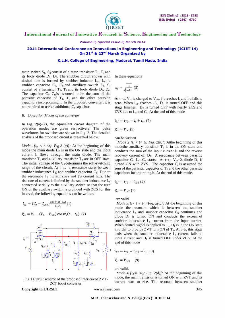
In Fig. 2(a)-(k), the equivalent circuit diagram of the
operation modes are given respectively. The pulse
waveforms for switches are shown in Fig. 3. The detailed
analysis of the proposed circuit is presented below.
Mode 1[t0 < t <t1: Fig.2 (a)]: At the beginning of this
mode the main diode DF is in the ON state and the input
current Ii flows through the main diode. The main
transistor T1 and auxiliary transistor T2 are in OFF state.
The initial voltage of the CS determines the soft-switching
range of the circuit. At t=t0, a resonance starts between
snubber inductance LS and snubber capacitor CS. Due to
the resonance T2 current rises and DF current falls. The
rise rate of current is limited by the snubber inductance LS
connected serially to the auxiliary switch so that the turn
ON of the auxiliary switch is provided with ZCS for this
interval, the following equations can be written:
𝑖𝐿𝑆 = 𝑉0 − 𝑉𝐶𝑆0 sin 𝑤𝑠 𝑡−𝑡0
𝐿𝑠𝑤𝑠 (1)
𝑉𝑐𝑠 = 𝑉0 − 𝑉0 − 𝑉𝑐𝑠0 cos𝑤𝑠 𝑡 − 𝑡0 (2)
Fig.1 Circuit scheme of the proposed interleaved ZVT-
ZCT boost converter.
In these equations
𝑤𝑠 = 1
𝐿𝑠𝐶𝑠 (3)
At t=t1, Vcs is charged to Vcs1, iT2 reaches Ii and iDF falls to
zero. When iDF reaches -Irr, DF is turned OFF and this
stage finishes. DF is turned OFF with nearly ZCS and
ZVS due to LS and Cr. At the end of this mode
𝑖𝐿𝑆 = 𝑖𝑇2 = 𝐼𝑖 + 𝐼𝑟𝑟 (4)
𝑉𝑐𝑠 = 𝑉𝑐𝑠1(5)
can be written.
Mode 2 [t1 < t< t2: Fig. 2(b)]: Atthe beginning of this
modethe auxiliary transistor T2 is in the ON state and
conducts the sum of the input current Ii and the reverse
recovery current of DF. A resonance between parasitic
capacitor Cr, LS, CS starts. At t=t2, Vcr=0, diode D1 is
turned ON with ZVS. The capacitor Cr is assumed the
sum of the parasitic capacitor of T1 and the other parasitic
capacitors incorporating it. At the end of this mode,
𝑖𝐿𝑆 = 𝑖𝑇2 = 𝑖𝐿𝑆2 (6)
𝑉𝑐𝑠 = 𝑉𝑐𝑠2 (7)
are valid.
Mode 3[t2< t < t3 : Fig. 2(c)]: At the beginning of this
mode the resonant which is between the snubber
inductance LS and snubber capacitor CS continues and
diode D1 is turned ON and conducts the excess of
snubber inductance LS current from the input current.
When control signal is applied to T1, D1 is in the ON state
in order to provide ZVT turn ON of T1. At t=t3, this stage
ends when the snubber inductance LS current falls to
input current and D1 is turned OFF under ZCS. At the
end of this mode
𝑖𝐿𝑆 = 𝑖𝑇2 = 𝑖𝐿𝑆3 = 𝐼𝑖 (8)
𝑉𝑐𝑠 = 𝑉𝑐𝑠3 (9)
are valid.
Mode 4 [t3<t <t4: Fig. 2(d)]: At the beginning of this
mode, the main transistor is turned ON with ZVT and its
current start to rise. The resonant between snubber
ISSN (Online) : 2319 - 8753 ISSN (Print) : 2347 - 6710
International Journal of Innovative Research in Science, Engineering and Technology
Volume 3, Special Issue 3, March 2014
2014 International Conference on Innovations in Engineering and Technology (ICIET’14)
On 21st & 22nd March Organized by
K.L.N. College of Engineering, Madurai, Tamil Nadu, India
Copyright to IJIRSET www.ijirset.com 346
M.R. Thansekhar and N. Balaji (Eds.): ICIET’14
inductance LS and snubber capacitor CS continues. For
this mode the following equation are derived:
𝑖𝐿𝑆 = 𝐼𝑖 cos𝑤𝑠 𝑡 − 𝑡3 −𝑉𝑐𝑠4
𝑤𝑠𝐿𝑠sin𝑤𝑠 𝑡 − 𝑡3 (10)
𝑉𝑐𝑠 = 𝑉𝑐𝑠4 cos𝑤𝑠 𝑡 − 𝑡3 + 𝐿𝑠𝑤𝑠𝐼𝑖 sin𝑤𝑠 𝑡 − 𝑡3 (11)
At t=t4, the current in the main transistor reaches to
the input current level and iLS becomes zero hence the
current through the auxiliary transistor reaches zero and
T2 is turned OFF. At the end of this mode,
𝑖𝐿𝑆 = 𝑖𝑇2 = 𝐼𝐿𝑆4 = 0 (12)
𝑉𝑐𝑠 = 𝑉𝑐𝑠4 (13)
are valid.
Mode 5 [t4 < t <t5 : Fig. 2(e)]: In this mode the diode D2
is turned ON with ZCS and its current starts to rise. The
resonant between snubber inductance and snubber
capacitance continues. The current through snubber
inductance iLs becomes negative, so the current through
the main transistor is higher than the input current in this
mode. The equation is expressed as follows:
𝑖𝐿𝑆 = −𝑉𝑐𝑠4
𝑤𝑠𝐿𝑠sin𝑤𝑠 𝑡 − 𝑡4 (14)
𝑉𝑐𝑠 = 𝑉𝑐𝑠4 cos𝑤𝑠 𝑡 − 𝑡4 (15)
At t=t5,the main transistor current decrease to the input
current level and iLS becomes zero. iD2 becomes zero and
it is turned OFF under ZCS. At the end of this mode,
(a)
(b)
(c )
(d)
(e)
(f)
(g)
(h)

ISSN (Online) : 2319 - 8753 ISSN (Print) : 2347 - 6710
International Journal of Innovative Research in Science, Engineering and Technology
Volume 3, Special Issue 3, March 2014
2014 International Conference on Innovations in Engineering and Technology (ICIET’14)
On 21st & 22nd March Organized by
K.L.N. College of Engineering, Madurai, Tamil Nadu, India
Copyright to IJIRSET www.ijirset.com 347
M.R. Thansekhar and N. Balaji (Eds.): ICIET’14
(i)
(j)
(k)
Fig. 2. Equivalent circuit schemes of the operation modes
in the proposed novel ZVT-ZCT-PWM boost converter.
(a) t0< t < t1. (b) t1< t < t2 . (c) t2< t < t3. (d) t3< t < t4. (e)
t4< t < t5(f) t5< t < t6. (g) t6< t < t7. (h) t7< t < t8. (i) t8< t
< t9. (j) t9< t <t10. (k) t10< t < t11 = t0 .
𝑖𝐿𝑆 = 𝑖𝑇2 = 𝐼𝐿𝑆5 = 0 (16)
𝑉𝑐𝑠 = 𝑉𝑐𝑠5 (17)
are valid.
Mode 6 [t5<t <t6: Fig. 2(f)]: In this mode main transistor
T1 conducts the input current Ii and snubber circuit is not
active. This mode is the ON state of the conventional
boost converter.
𝐼𝑇1 = 𝐼𝑖 (18)
are valid.
Mode 7 [t6 <t <t7: Fig. 2(g)]: In this mode the control
signal is applied to auxiliary transistor T2, a new
resonance between snubber inductance LS and snubber
capacitor CS. starts through CS-LS-T2-T1. The equations
can be expressed as follows,
𝑖𝐿𝑆 = −𝑉𝑐𝑠5
𝑤𝑠𝐿𝑠sin𝑤𝑠 𝑡 − 𝑡5 (19)
𝑉𝑐𝑠 = 𝑉𝑐𝑠5 cos𝑤𝑠 𝑡 − 𝑡5 (20)
The auxiliary transistor T2 is turned ON with ZCS due to
the snubber inductance LS. The main transistor T1 current
falls with the rise in snubber inductance current.At t=t7,
when the current of T2 reaches to the input current level,
the main transistor current becomes zero and this mode
finishes.At the end of this mode,
𝑖𝐿𝑆 = 𝑖𝑇2 = 𝐼𝐿𝑆7 = 𝐼𝑖 (21)
𝑉𝑐𝑠 = 𝑉𝑐𝑠7 (22)
are valid
Mode 8 [t7 <t <t8: Fig. 2(h)]: At the beginning of this
mode, D1 is turned ON with ZCS. If T1 turned OFF when
D1 is ON, T1 turns OFF with ZVS and ZCS. D1 conducts
the excess of iLS from the input current. The resonance
between LS and CS continues. At=t8, iD1 reaches –Irr and
turns OFF, and this stage ends. At the end of this mode
𝑖𝐿𝑆 = 𝑖𝑇2 = 𝐼𝐿𝑆8 = 𝐼𝑖 − 𝐼𝑟𝑟 (23)
𝑉𝑐𝑠 = 𝑉𝑐𝑠8 = 𝑉𝑐𝑠0(24)
are valid.
Mode 9 [t8 <t <t9: Fig. 2(i)]: In the beginning of this
mode, a resonance between parasitic capacitor Cr,
snubber inductor LS and snubber capacitor CS starts. At
t=t9, iLS falls to zero and the capacitor Cr is charged from
zero to Vcs8 with this resonance. The auxiliary transistor
T2 is turned OFF with ZCS. At the end of this mode
𝑖𝐿𝑆 = 𝑖𝑇2 = 𝐼𝐿𝑆9 = 0(25)
𝑉𝑐𝑠 = 𝑉𝑐𝑠9 = 𝑉𝑐𝑠0(26)
are valid.
Mode 10 [t9 <t <t10: Fig. 2(j)]: In this mode Cr is charged
linearly under the input current. At instant t10Cr voltage
reaches the output voltage Vo, and the main diode DF is
turned ON with ZVS.
Mode 11 [t10<t<t11: Fig. 2(k)]: This mode is the OFF
state of the conventional boost converter. During this
mode, the main diode DF continues conducting the input

ISSN (Online) : 2319 - 8753 ISSN (Print) : 2347 - 6710
International Journal of Innovative Research in Science, Engineering and Technology
Volume 3, Special Issue 3, March 2014
2014 International Conference on Innovations in Engineering and Technology (ICIET’14)
On 21st & 22nd March Organized by
K.L.N. College of Engineering, Madurai, Tamil Nadu, India
Copyright to IJIRSET www.ijirset.com 348
M.R. Thansekhar and N. Balaji (Eds.): ICIET’14
current Ii and the snubber circuit is not active. For this
mode
𝑖𝐷𝐹 = 𝐼𝑖 (27)
can be written.
Mode 12-22:since two cells of the converter are identical
and operating with the same frequency and duty cycles
and there is only 1800 phase shift between these two cells,
the circuit behavior during operation modes of 11-22 is
similar to that of during modes of 1–11. The circuit
analysis of the converter during the last eleven modes is
similar to that of the first eleven modes and can be
Achieved by replacing T1, T2, D1, D2, DF, LF, Cr, LS,
CS,Vcs0 with T3, T4, D3, D4, DF1, LF1, Cr1, LS1, CS1,Vcs1
respectively.
III DESIGN PROCEDURE
The design procedure for the proposed interleaved
ZVT-ZCT boost converter is presented in this section.
1. Operating Requirements:
Output power Pout: 1KW
Input voltage Vin: 200V DC
Switching frequency (fsw): 100 KHZ
Output voltage (Vo): 400V
2. Input and Output Parameters:
The relationship between the duty cycle and the
Output/input ratio for interleaved boost converter is
𝑉𝑜
𝑉𝑖𝑛=
1
1−𝐷 (28)
Fig. 3 Pulse waveforms for switches
3. Inductor Current Ripple Peak-To-Peak Amplitude:
The inductor current ripple peak-peak amplitude
is given by
∆𝐼𝑙1𝑙2 =𝑉𝑖𝑛 𝐷
𝑓𝑠𝑤 𝐿 (29)
Where fsw is the switching frequency, D is the duty
cycle, Vin is the input Voltage and L is the inductance.
4. Output Voltage Ripple:
Since the load and output capacitor are supplied
through two diodes DF and DF1, the frequency of the
output ripple current is twice the switching frequency.
This decreases the output ripple voltage∆𝑉𝑜 . The output
capacitor is determined as,
𝐶 =𝑉𝑜𝐷𝐹
𝑅∆𝑉𝑜 (30)
5. Selection of Snubber Inductor:
The snubber inductance can be selected to
provide the following conditions with reference to [15].
Here, tr2 is rise time of the auxiliary switch. Vcs1 is
assumed constant in tr2 duration
𝑉0−𝑉𝑐𝑠1
𝐿𝑠𝑡𝑟2 ≤ 𝐼𝑖𝑚𝑎𝑥 (31)
ISSN (Online) : 2319 - 8753 ISSN (Print) : 2347 - 6710
International Journal of Innovative Research in Science, Engineering and Technology
Volume 3, Special Issue 3, March 2014
2014 International Conference on Innovations in Engineering and Technology (ICIET’14)
On 21st & 22nd March Organized by
K.L.N. College of Engineering, Madurai, Tamil Nadu, India
Copyright to IJIRSET www.ijirset.com 349
M.R. Thansekhar and N. Balaji (Eds.): ICIET’14
To turn ON auxiliary switch with ZCS, the required Series
inductor Ls is calculated as,
𝐿𝑆 ≥400−150
5 2 ∗ 10−6 ≥ 0.1𝑚𝐻(32)
The value of Ls is selected as the smallest possible value
as 1mH in order to decrease ZCT duration.
6. Selection of Snubber Capacitor:
The snubber capacitor Cs is determined depending on the
transient intervals.The sum of the transient intervals
isselected to be smaller than 20% oftransient intervals is
equal to the resonant period tR
𝑡𝑅 < 𝑇𝑠 ∗ 20
100 (33)
𝑡𝑅 = 2𝜋 𝐿𝑠𝐶𝑠 (34)
The value of Cs is selected as 33𝜇F to obtain appropriate
ZVT duration.
IV. SIMULATION RESULTS
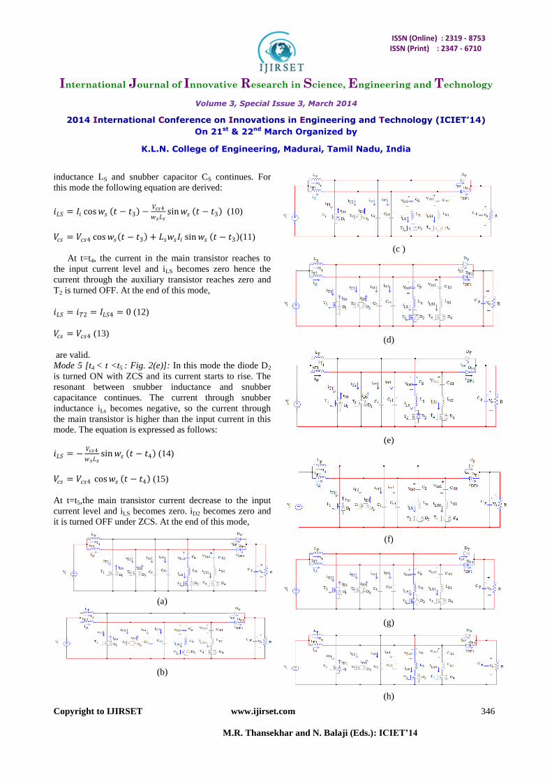
The computer simulation of proposed converter is done
using MATLAB/SIMULINK and the results are
presented. The simulation result of the output voltage and
output current are shown in Fig. 4.Soft switching in the
auxiliary switch is shown in the Fig.6. Fig.7. Shows the
Ripple content in the output voltage.Ripple content in the
output voltage is low due to interleavingtechnique. Ripple
content in the output voltage is calculated by finding the
difference between peak –to–peak voltages. Due to reduce
in the ripple content in the output voltage efficiency of the
converter is increased.
Fig.4 input and output voltage, current waveforms
(Vin=200V, Ii=5A, Vout=400V, Iout=2.5A)
Soft switching in the main switch is shown in the Fig.5
Comparisons of the output ripple voltage and THD of
conventional ZVT-ZCT boost converter and interleaved
ZVT-ZCT boost converter are shown in Table I.
Table I
TYPE OUTPUT
RIPPLE
VOLTAGE
THD
ZVT-ZCT
Boost Converter
32mV 105.65%
Interleaved
ZVT-ZCT
Boost Converter
2.8mV 76.02%

ISSN (Online) : 2319 - 8753 ISSN (Print) : 2347 - 6710
International Journal of Innovative Research in Science, Engineering and Technology
Volume 3, Special Issue 3, March 2014
2014 International Conference on Innovations in Engineering and Technology (ICIET’14)
On 21st & 22nd March Organized by
K.L.N. College of Engineering, Madurai, Tamil Nadu, India
Copyright to IJIRSET www.ijirset.com 350
M.R. Thansekhar and N. Balaji (Eds.): ICIET’14
Fig.5 soft switching of the main switch
Fig.6 soft switching of the auxiliary switch
Fig.7 Ripple voltage waveform
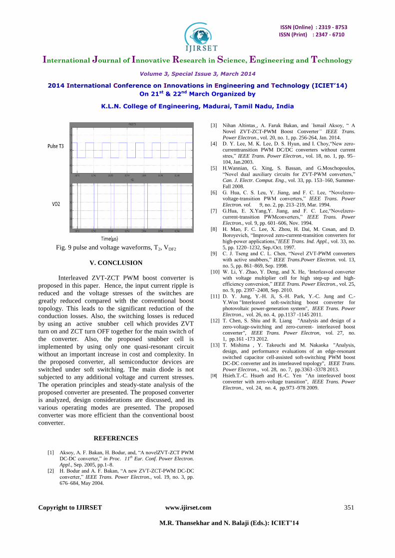
Voltage across the main diode DF1, DF2 is shown in the
Fig. 8 and Fig. 9.
Fig. 8 pulse and voltage waveforms, T1, VDF1
ISSN (Online) : 2319 - 8753 ISSN (Print) : 2347 - 6710
International Journal of Innovative Research in Science, Engineering and Technology
Volume 3, Special Issue 3, March 2014
2014 International Conference on Innovations in Engineering and Technology (ICIET’14)
On 21st & 22nd March Organized by
K.L.N. College of Engineering, Madurai, Tamil Nadu, India
Copyright to IJIRSET www.ijirset.com 351
M.R. Thansekhar and N. Balaji (Eds.): ICIET’14
Fig. 9 pulse and voltage waveforms, T2, VDF2
V. CONCLUSION
Interleaved ZVT-ZCT PWM boost converter is
proposed in this paper. Hence, the input current ripple is
reduced and the voltage stresses of the switches are
greatly reduced compared with the conventional boost
topology. This leads to the significant reduction of the
conduction losses. Also, the switching losses is reduced
by using an active snubber cell which provides ZVT
turn on and ZCT turn OFF together for the main switch of
the converter. Also, the proposed snubber cell is
implemented by using only one quasi-resonant circuit
without an important increase in cost and complexity. In
the proposed converter, all semiconductor devices are
switched under soft switching. The main diode is not
subjected to any additional voltage and current stresses.
The operation principles and steady-state analysis of the
proposed converter are presented. The proposed converter
is analyzed, design considerations are discussed, and its
various operating modes are presented. The proposed
converter was more efficient than the conventional boost
converter.
REFERENCES
[1] Aksoy, A. F. Bakan, H. Bodur, and, ―A novelZVT-ZCT PWM
DC-DC converter,‖ in Proc. 11th Eur. Conf. Power Electron.
Appl., Sep. 2005, pp.1–8. [2] H. Bodur and A. F. Bakan, ―A new ZVT-ZCT-PWM DC-DC
converter,‖ IEEE Trans. Power Electron., vol. 19, no. 3, pp.
676–684, May 2004.
[3] Nihan Altintas¸, A. Faruk Bakan, and ˙Ismail Aksoy, ― A
Novel ZVT-ZCT-PWM Boost Converter” IEEE Trans.
Power Electron., vol. 20, no. 1, pp. 256-264, Jan. 2014. [4] D. Y. Lee, M. K. Lee, D. S. Hyun, and I. Choy,―New zero-
currenttransition PWM DC/DC converters without current
stres,‖ IEEE Trans. Power Electron., vol. 18, no. 1, pp. 95–104, Jan.2003.
[5] H.Wannian, G. Xing, S. Bassan, and G.Moschopoulos,
―Novel dual auxiliary circuits for ZVT-PWM converters,‖ Can. J. Electr. Comput. Eng., vol. 33, pp. 153–160, Summer-
Fall 2008.
[6] G. Hua, C. S. Leu, Y. Jiang, and F. C. Lee, ―Novelzero-voltage-transition PWM converters,‖ IEEE Trans. Power
Electron. vol. 9, no. 2, pp. 213–219, Mar. 1994.
[7] G.Hua, E. X.Yang,Y. Jiang, and F. C. Lee,―Novelzero-current-transition PWMconverters,‖ IEEE Trans. Power
Electron., vol. 9, pp. 601–606, Nov. 1994.
[8] H. Mao, F. C. Lee, X. Zhou, H. Dai, M. Cosan, and D. Boroyevich, ―Improved zero-current-transition converters for
high-power applications,‖IEEE Trans. Ind. Appl., vol. 33, no.
5, pp. 1220–1232, Sep./Oct. 1997. [9] C. J. Tseng and C. L. Chen, ―Novel ZVT-PWM converters
with active snubbers,‖ IEEE Trans.Power Electron. vol. 13,
no. 5, pp. 861–869, Sep. 1998. [10] W. Li, Y. Zhao, Y. Deng, and X. He, ‗Interleaved converter
with voltage multiplier cell for high step-up and high-efficiency conversion,‖ IEEE Trans. Power Electron., vol. 25,
no. 9, pp. 2397–2408, Sep. 2010.
[11] D. Y. Jung, Y.-H. Ji, S.-H. Park, Y.-C. Jung and C.-Y.Won "Interleaved soft-switching boost converter for
photovoltaic power-generation system", IEEE Trans. Power
Electron., vol. 26, no. 4, pp.1137 -1145 2011. [12] T. Chen, S. Shiu and R. Liang "Analysis and design of a
zero-voltage-switching and zero-current- interleaved boost
converter", IEEE Trans. Power Electron, vol. 27, no. 1, pp.161 -173 2012.
[13] T. Mishima , Y. Takeuchi and M. Nakaoka "Analysis,
design, and performance evaluations of an edge-resonant switched capacitor cell-assisted soft-switching PWM boost
DC-DC converter and its interleaved topology", IEEE Trans.
Power Electron., vol. 28, no. 7, pp.3363 -3378 2013. [14] Hsieh.T.-C. Hsueh and H.-C. Yen "An interleaved boost
converter with zero-voltage transition", IEEE Trans. Power
Electron., vol. 24, no. 4, pp.973 -978 2009.
Related Documents