CHAPTER 18 ELECTRICAL PROPERTIES PROBLEM SOLUTIONS Ohm’s Law Electrical Conductivity 18.1 (a) Compute the electrical conductivity of a 5.1-mm (0.2-in.) diameter cylindrical silicon specimen 51 mm (2 in.) long in which a current of 0.1 A passes in an axial direction. A voltage of 12.5 V is measured across two probes that are separated by 38 mm (1.5 in.). (b) Compute the resistance over the entire 51 mm (2 in.) of the specimen. Solution This problem calls for us to compute the electrical conductivity and resistance of a silicon specimen. (a) We use Equations 18.3 and 18.4 for the conductivity, as s = 1 r = Il VA = Il V p d 2 æ è ç ö ø ÷ 2 And, incorporating values for the several parameters provided in the problem statement, leads to s = ( 0. 1 A)( 38 ´ 10 - 3 m) ( 12. 5 V)(p) 5. 1 ´ 10 - 3 m 2 æ è ç ö ø ÷ 2 = 14.9 ( W - m) -1 (b) The resistance, R, may be computed using Equations 18.2 and 18.4, as R = rl A = l sA = l sp d 2 æ è ç ö ø ÷ 2 = 51 ´ 10 - 3 m 14. 9( W- m) - 1 [ ] (p) 5. 1 ´ 10 - 3 m 2 æ è ç ö ø ÷ 2 = 168 W

Welcome message from author
This document is posted to help you gain knowledge. Please leave a comment to let me know what you think about it! Share it to your friends and learn new things together.
Transcript

CHAPTER 18
ELECTRICAL PROPERTIES
PROBLEM SOLUTIONS
Ohm’s Law
Electrical Conductivity
18.1 (a)
Compute the electrical conductivity of a 5.1-
mm (0.2-in.) diameter cylindrical silicon specimen
51 mm (2 in.) long in which a current of 0.1 A passes in an axial direction. A voltage of 12.5 V is measured across
two probes that are separated by 38 mm (1.5 in.).
(b)
Compute the resistance over the entire 51 mm (2 in.) of the specimen.
Solution
This problem calls for us to compute the electrical conductivity and resistance of a silicon specimen.
(a) We use Equations 18.3 and 18.4 for the conductivity, as
s =
1
r=
Il
VA=
Il
Vpd
2
æ
è ç
ö
ø ÷
2
And, incorporating values for the several parameters provided in the problem statement, leads to
s =(
0.
1 A)(
38 ´
10-
3 m)
(
12.
5 V)(p)
5.
1 ´
10-
3 m
2
æ
è ç
ö
ø ÷
2=
14.9 (W - m)
-1
(b) The resistance, R
, may be computed using Equations 18.2 and 18.4, as
R =rl
A=
l
sA =
l
spd
2
æ
è ç
ö
ø ÷
2
=
51 ´
10-
3 m
14.
9 (W - m)-
1[ ] (p)
5.
1 ´
10-
3 m
2
æ
è ç
ö
ø ÷
2=
168 W

18.2
A copper wire 100 m long must experi
ence a voltage drop of less than 1.5 V when a current of 2.5 A
passes through it. Using the data in Table 18.1, compute the minimum diameter of the wire.
Solution
For this problem, given that a copper wire 100 m long must experience a voltage drop of l
ess than 1.5 V when
a current of 2.5 A passes through it, we are to compute the minimum diameter of the wire. Combining Equations 18.3
and 18.4 and solving for the cross-sectional area A leads to
A =Ilr
V=
Il
Vs
From Table 18.1, for copper s
= 6
.0 ´
10
7 (W-m)-
1. Furthermore, inasmuch as
A = pd
2
æ
è ç
ö
ø ÷
2
for a cylindrical wire, then
pd
2
æ
è ç
ö
ø ÷
2
=Il
Vs
or
d =
4 Il
pVs
When values for the several parameters given in the problem statement are incorporated into this expression, we get
d =(
4)(
2.
5 A)(
100 m)
(p)(
1.
5 V)
6.
0 ´
10
7 (W - m)-
1[ ]
= 1.88 ´
10-
3
m = 1.88 mm

18.3
An aluminum wire 4 mm in diameter is to offer a resistance of no more than 2.5 W . Using the data in
Table 18.1, compute the maximum wire length.
Solution
This problem asks that we
compute, for an aluminum wire 4 mm in diameter, the maximum length such that
the resistance will not exceed 2.5 W
. From Table 18.1 for aluminum, s
= 3.8 ´
10
7 (W-m)-
1. If d is the diameter then,
combining Equations 18.2 and 18.4 leads to
l =RA
r= RsA = Rsp
d
2
æ
è ç
ö
ø ÷
2
=
(2.5 W)
3.
8 ´
10
7 (W - m)-
1[ ](p)
4 ´
10-
3 m
2
æ
è ç
ö
ø ÷
2
=
1194 m

18.4
Demonstrate that the two Ohm’s law expressions, Equations 18.1 and 18.5, are equivalent.
Solution
Let us demonstrate, by appropriate substitution and algebraic manipulation, that Equation 18.5 may be made
to tak
e the form of Equation 18.1. Now, Equation 18.5 is just
J = sE
(In this equation we represent the electric field with an “E”.) But, by definition, J is just the current density, the
current per unit cross-sectional area, or
J =I
A. Also, the electric field is defined by
E =V
l. And, substituting these
expressions into Equation 18.5 leads to
I
A= s
V
l
But, from Equations 18.2 and 18.4
s =l
RA
and
I
A=
l
RA
æ
è ç
ö
ø ÷
V
l
æ
è ç
ö
ø ÷
Solving for V from this expression gives V = IR
, which is just Equation 18.1.

18.5 (a)
Using the data in Table 18.1, compute the resistance of a copper wire 3 mm (0.12 in.) in diameter
and 2 m (78.7 in.) long. (b) What would be the current flow if the potential drop across the ends of the wire is 0.05
V? (c) What is the current density? (d) What is the magnitude of the electric field across the ends of the wire?
Solution
(a) In order to compute the resistance of this copper wire it is necessary to employ Equations 18.2 and 18.4.
Solving for the resistance in terms of the conductivity,
R =r l
A=
l
sA=
l
spd
2
æ
è ç
ö
ø ÷
2
From Table 18.1, the conductivity of copper is 6.0 ´
10
7 (W-m)-
1, and
R =l
spd
2
æ
è ç
ö
ø ÷
2=
2 m
6.
0 ´
10
7 (W - m)-
1[ ](p)
3 ´
10-
3 m
2
æ
è ç
ö
ø ÷
2
= 4.7 ´
10-
3 W
(b) If V
= 0.05 V then, from Equation 18.1
I =V
R=
0.
05 V
4.
7 ´
10-
3 W=
10.6 A
(c) The current density is just
J =I
A=
I
pd
2
æ
è ç
ö
ø ÷
2=
10.
6 A
p
3 ´
10-
3 m
2
æ
è ç
ö
ø ÷
2=
1.
5 ´
10
6 A/m
2
(d) The electric field is just
E =V
l=
0.
05 V
2 m=
2.
5 ´
10
-2 V/m

Electronic and Ionic Conduction
18.6 What is the distinction between electronic and ionic conduction?
Solution
When a current arises from a flow of electrons, the conduction is termed electronic; for ionic conduction,
the current results from the net motion of charged ions.

Energy Band Structures in Solids
18.7 How does the electron structure of an isolated atom differ from that of a solid material?
Solution
For an isolated atom, there exist discrete electron energy states (arranged into shells and subshells); each
state may be occupied by, at most, two electrons, which must have opposite spins. On the other hand, an electron
band structure is found for solid materials; within each band exist closely spaced yet discrete electron states, each of
which may be occupied by, at most, two electrons, having opposite spins. The number of electron states in each
band will equal the total number of corresponding states contributed by all of the atoms in the solid.

Conduction in Terms of Band and Atomic Bonding Models
18.8 In terms of electron energy band structure, discuss reasons for the difference in electrical
conductivity between metals, semiconductors, and insulators.
Solution
For metallic materials, there are vacant electron energy states adjacent to the highest filled state; thus, very
little energy is required to excite large numbers of electrons into conducting states. These electrons are those that
participate in the conduction process, and, because there are so many of them, metals are good electrical conductors.
There are no empty electron states adjacent to and above filled states for semiconductors and insulators,
but rather, an energy band gap across which electrons must be excited in order to participate in the conduction
process. Thermal excitation of electrons will occur, and the number of electrons excited will be less than for metals,
and will depend on the band gap energy. For semiconductors, the band gap is narrower than for insulators;
consequently, at a specific temperature more electrons will be excited for semiconductors, giving rise to higher
conductivities.

Electron Mobility
18.9 Briefly tell what is meant by the drift velocity and mobility of a free electron.
Solution
The drift velocity of a free electron is the average electron velocity in the direction of the force imposed by
an electric field.
The mobility is the proportionality constant between the drift velocity and the electric field. It is also a
measure of the frequency of scattering events (and is inversely proportional to the frequency of scattering).

18.10 (a) Calculate the drift velocity of electrons in germanium at room temperature and when the
magnitude of the electric field is 1000 V/m. (b) Under these circumstances, how long does it take an electron to
traverse a 25-
mm (1-in.) length of crystal?
Solution
(a) The drift velocity of electrons in Ge may be determined using Equation 18.7. Since the room temperature
mobility of electrons is 0.38 m
2/V-
s (Table 18.3), and the electric field is 100
0 V/m (as stipulated in the problem
statement),
vd = meE
= (
0.38 m
2/V - s)
(1000 V/m) =
380 m/s
(b) The time, t, required to traverse a given length, l
(= 25 mm), is just
t =l
vd
=
25 ´
10-
3 m
380 m/s=
6.6 ´
10
-5 s
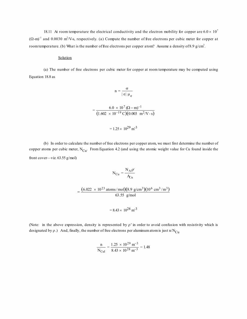
18.11 At room temperature the electrical conductivit
y and the electron mobility for copper are 6.0 ´
10
7
(W-m)-
1
and 0.0030 m
2/V-s, respectively. (a) Compute the number of free electrons per cubic meter for copper at
room temperature. (b) What is the number of free electrons per copper atom? Assume a density of 8.9 g/cm
3.
Solution
(a) The number of free electrons per cubic meter for copper at room temperature may be computed using
Equation 18.8 as
n =s
| e | me
=
6.
0 ´
10
7 (W - m)-
1
(
1.
602 ´
10-
19 C)(
0.
003 m
2/V - s)
= 1.25 ´
10
29 m-
3
(b) In order to calculate the number of free electrons per copper atom, we must first determine the number of
copper atoms per cubic meter, NCu
. From Equation 4.2 (and using the atomic weight value for Cu found inside the
front cover—
viz. 63.55 g/mol)
NCu =NA ¢ r
ACu
=(
6.
022 ´
10
23 atoms /mol)(
8.
9 g/cm
3)(
10
6 cm
3 /m
3)
63.
55 g/mol
= 8.43 ´
10
28 m-
3
(Note: in the above expression, density is represented by r ' in order to avoid confusion with resistivity which is
designated by r.) And, finally, the number of free electrons per aluminum atom is just n/NCu
n
NCul
=
1.
25 ´
10
29 m-
3
8.
43 ´
10
28 m-
3=
1.48

18.12 (a) Calculate the number of free
electrons per cubic meter for gold assuming that there are 1.5 free
electrons per gold atom. The electrical conductivity and density for Au are 4.3 ´
10
7 (W-m)-
1
and 19.32 g/cm
3,
respectively. (b) Now compute the electron mobility for Au.
Solution
(a) This portion of the problem asks that we calculate, for gold, the number of free electrons per cubic meter
(n
) given that there are 1.5 free electrons per gold atom, that the electrical conductivity is 4.3 ´
10
7 (W-m)-
1, and that
the density
(rAu' )
is 19.32 g/cm
3. (Note: in this discussion, the density of silver is represented by
rAu' in order to
avoid confusion with resistivity which is designated by r.) Since n
= 1.5NAu, and NAu
is defined in Equation 4.2
(and using the atomic weight of Au found inside the front cover—
viz 196.97 g/mol), then
n =
1.5NAu =
1.5 rAu
' NA
AAu
é
ë
ê ê
ù
û
ú ú
=
1.5 (
19.
32 g/cm
3)(
6.
022 ´
10
23 atoms / mol)
196 .
97 g/mol
é
ë ê
ù
û ú
= 8.86 ´
10
22 cm-
3
= 8.86 ´
10
28 m-
3
(b) Now we are asked to compute the electron mobility, me
. Using Equation 18.8
me =s
n | e |
=
4.
3 ´
10
7 (W - m)-
1
(
8.
86 ´
10
28 m-
3)(
1.
602 ´
10-
19C)=
3.03 ´
10
-3 m
2/V - s

Electrical Resistivity of Metals
18.13
From Figure 18.38, estimate the value of A in Equation 18.11 for zinc as an impurity in copper–zinc
alloys.
Solution
We want to solve for the parameter A in Equati
on 18.11 using the data in Figure 18.38. From Equation 18.11
A =ri
ci (
1 - ci )
However, the data plotted in Figure 18.38 is the total resistivity, rtotal, and includes both impurity (ri) and thermal
(rt
) contributions (Equation 18.9). The value of rt is taken as the resistivity at ci
= 0 in Figure 18.38, which has a
value of 1.7 ´
10-
8 (W-m); this must be subtracted out. Below are tabulated values of A determined at ci
= 0.10, 0.20,
and 0.30, including other data that were used in the computations. (Note: the ci values were taken from the upper
horizontal axis of Figure 18.38, since it is graduated in atom percent zinc.)
ci
1 – ci rtotal (W-m) ri (W-m) A (W-m)
0.10
0.90
4.0 ´
10-
8
2.3 ´
10-
8
2.56 ´
10-
7
0.20
0.80
5.4 ´
10-
8
3.7 ´
10-
8
2.31 ´
10-
7
0.30
0.70
6.15 ´
10-
8
4.45 ´
10-
8
2.12 ´
10-
7
So, there is a slight decrease of A with increasing ci.

18.14 (a)
Using the data in Figure 18.8, determine the values of ρ
0
and a from Equation 18.10 for pure
copper. Take the temperature T to be in degrees Celsius. (b) Determine the value of A in Equation 18.11 for nickel
as an impurity in copper, using the data in Figure 18.8. (c) Using the results of parts (a) and (b), estimate the
electrical resistivity of copper containing 1.75 at% Ni at 100°C.
Solution
(a) Perhaps the easiest way to determine the values of r
0 and a
in Equation 18.10 for pure copper in Figure
18.8, is to set up two simultaneous equations using two resistivity values (labeled rt
1 and rt
2) taken at two
corresponding temperatures (T
1 and T
2). Thus,
rt
1 = r
0 + aT
1
rt
2 = r
0 + aT
2
And solving these equations simultaneously lead to the following expressions for a and r
0:
a =rt
1 - rt
2
T
1 - T
2
r
0 = rt
1 - T
1
rt
1 - rt
2
T
1 -T
2
é
ë
ê ê
ù
û
ú ú
= rt
2 - T
2
rt
1 - rt
2
T
1 - T
2
é
ë
ê ê
ù
û
ú ú
From Figure 18.8, let us take T
1 = –
150°C, T
2 = –
50°C, which gives rt
1
= 0.6 ´
10-
8 (W-m), and rt
2
= 1.25 ´
10-
8 (W-m).
Therefore
a =rt
1 - rt
2
T
1 - T
2
= (
0.6 ´
10
-8) - (
1.25 ´
10
-8)[ ]W - m( )
-
150°C - (-
50°C)
6.5 ´
10-
11 (W-m)/°C

and
r
0 = rt
1 - T
1
rt
1 - rt
2
T
1 -T
2
é
ë
ê ê
ù
û
ú ú
= (
0.6 ´
10
-8) - (-
150) (
0.6 ´
10
-8) - (
1.25 ´
10
-8)[ ]W - m( )
-
150°C - (-
50°C)
= 1.58 ´
10-
8 (W-m)
(b) For this part of the problem, we want to calculate A
from Equation 18.11
ri = Aci (
1 - ci)
In Figure 18.8, curves are plotted for three ci
values (0.0112, 0.0216, and 0.0332). Let us find A for each of these ci's by
taking a rtotal
from each curve at some temperature (say 0°C) and then subtracting out ri for pure copper at this
same temperature (which is 1.7 ´
10-
8 W-m). Below is tabulated values of A determined from these three ci values,
and other data that were used in the computations.
ci
1 – ci rtotal (W-m) ri (W-m) A (W-m)
0.0112
0.989
3.0 ´
10-
8
1.3 ´
10-
8
1.17 ´
10-
6
0.0216
0.978
4.2 ´
10-
8
2.5 ´
10-
8
1.18 ´
10-
6
0.0332
0.
967
5.5 ´
10-
8
3.8 ´
10-
8
1.18 ´
10-
6
The average of these three A
values is 1.18 ´
10-
6 (W-m).
(c) We use the results of parts (a) and (b) to estimate the electrical resistivity of copper containing 1.75 at%
Ni (ci
= 0.0175) at 100°C. The total resistivity is just
rtotal = rt + ri
Or incorporating the expressions for rt and ri
from Equations 18.10 and 18.11, and the values of r
0, a , and A
determined above, leads to
rtotal = (r
0 + aT) + Aci (
1 - ci)

=
1
.58 ´
10
-8 (W - m) + [
6.5 ´
10 -
11 (W - m) /°C](
100 °C)
+ [
1.18 ´
10 -
6 (W - m)](
0.
0175) (
1 -
0.0175)
= 4.
25 ´
10-
8 (W-m)

18.15 Determine the electrical conductivity of a Cu-
Ni alloy that has a yield strength of 125 MPa (18,000
psi). You will find Figure 7.16 helpful.
Solution
We are asked to determine the electrical conductivity of a Cu-Ni alloy that h
as a yield strength of 125 MPa.
From Figure 7.16b
, the composition of an alloy having this tensile strength is about 20 wt% Ni. For this composition,
the resistivity is about 27 ´
10-
8 W-
m (Figure 18.9). And since the conductivity is the reciprocal of the resistivity,
Equation 18.4, we have
s =
1
r=
1
27 ´
10-
8 W - m=
3.70 ´
10
6 (W - m)
-1

18.16
Tin bronze has a composition of 92 wt% Cu and 8 wt% Sn, and consists of two phases at room
temperature: an a phase, which is copper containing a very small amount of tin in solid solution, and an e phase,
which consists of approximately 37 wt% Sn. Compute the room temperature conductivity of this alloy given the
following data:
Phase Electrical Resistivity
(Ω-m) Density (g/cm
3)
α
1.88 × 10–
8
8.94
e
5.32 × 10–
7
8.25
Solution
This problem asks for us to compute the room-temperature conductivity of a two-phase Cu-Sn alloy which
composition is 92 wt% Cu-
8 wt% Sn. It is first necessary for us to determine the volume fractions of the a and e
phases, after which the resistivity (and
subsequently, the conductivity) may be calculated using Equation 18.12.
Weight fractions of the two phases are first calculated using the phase diagram information provided in the problem.
We may represent a portion of the phase diagram near room temperature as follows:
Applying the lever rule to this situation
Wa =Ce - C
0
Ce - Ca
=
37 -
8
37 -
0=
0.784
We =C
0 - Ca
Ce - Ca
=
8 -
0
37 -
0=
0.216

We must now convert these mass fractions into volume fractions using the phase densities given in the problem
statement. (Note: in the following expressions, density is represented by r ' in order to avoid confusion with
resistivity which is designated by r
.) Utilization of Equations 9.6a and 9.6b leads to
Va =
Wa
r'aWa
r'a+
Wer'e
=
0.
784
8.
94 g/cm
3
0.
784
8.
94 g/cm
3+
0.
216
8.
25 g/cm
3
= 0.770
Ve =
Wer'e
Wa
r'a+
Wer'e
=
0.
216
8.
25 g/cm
3
0.
784
8.
94 g/cm
3+
0.
216
8.
25 g/cm
3
= 0.230
Now, using Equation 18.12
r = raVa + reVe
= (
1.88 ´
10
-8 W - m)
(0.770) + (
5.32 ´
10
-7 W - m)
(0.230)
= 1.368 ´
10-
7 W-m

Finally, for the conductivity (Equation 18.4)
s =
1
r=
1
1.
368 ´
10-
7 W - m=
7.31 ´
10
6 (W - m)
-1

18.17
A cylindrical metal wire 2 mm (0.08 in.) in diame
ter is required to carry a current of 10 A with a
minimum of 0.03 V drop per foot (300 mm) of wire. Which of the metals and alloys listed in Table 18.1 are possible
candidates?
Solution
We are asked to select which of several metals may be used for a
2 mm diameter wire to carry 10 A, and have
a voltage drop less than 0.03 V per foot (300 mm). Using Equations 18.3 and 18.4, let us determine the minimum
conductivity required, and then select from Table 18.1, those metals that have conductivities greater than this value.
Combining Equations 18.3 and 18.4, the minimum conductivity is just
s =
1
r=
Il
VA=
Il
Vpd
2
æ
è ç
ö
ø ÷
2
=(
10 A)(
300 ´
10-
3 m)
(
0.
03 V) (p)
2 ´
10-
3 m
2
æ
è ç
ö
ø ÷
2=
3.2 ´
10
7 (W - m)
-1
Thus, from Table 18.1, only aluminum, gold, copper, and silver are candidates.

Intrinsic Semiconduction
18.18 (a)
Using the data presented in Figure 18.16, determine the number of free electrons per atom for
intrinsic germanium and silicon at room temperature (298 K). The densities for Ge and Si are 5.32 and 2.33 g/cm
3,
respectively.
(b) Now explain the difference in these free-electron-per-atom values.
Solution
(a) For this part of the problem, we first read, from Figure 18.16, the number of free electrons (i.e., the
intrinsic carrier concentration) at room temperature (298 K). These values are ni
(Ge) = 5 ´
1
0
19 m-
3 and ni
(Si) = 7 ´
10
16 m-
3.
Now, the number of atoms per cubic meter for Ge and Si (NGe and NSi, respectively) may be determined
using Equation 4.2 which involves the densities (
rGe' and
rSi' ) and atomic weights (AGe and ASi). (Note: here we
use r ' to represent density in order to avoid confusion with resistivity, which is designated by r. Also, the atomic
weights for Ge and Si, 72.64 and 28.09 g/mol, respectively, are found inside the front cover.) Therefore,
NGe =NArGe
'
AGe
=(
6.
022 ´
10
23 atoms/mol)(
5.
32 g/cm
3)(
10
6 cm
3/m
3)
72.
64 g/mol
= 4.41 ´
10
28 atoms/m
3
Similarly, for Si
NSi =NArSi
'
ASi
=(
6.
022 ´
10
23 atoms /mol)(
2.
33 g/cm
3)(
10
6 cm
3/m
3)
28.
09 g/mol
= 5.00 ´
10
28 atoms/m
3
Finally, the ratio of the number of free electrons per atom is calculated by dividing ni by N. For Ge

ni (Ge)
NGe
=
5 ´
10
19 electrons /m
3
4.
41 ´
10
28 atoms /m
3
1.13 ´
10-
9 electron/atom
And, for Si
ni(Si)
NSi
=
7 ´
10
16 electrons /m
3
5.
00 ´
10
28 atoms /m
3
= 1.40 ´
10-
12 electron/atom
(b) The difference is due to the magnitudes of the band gap energies (Table 18.3). The band gap energy at
room te
mperature for Si (1.11 eV) is larger than for Ge (0.67 eV), and, consequently, the probability of excitation across
the band gap for a valence electron is much smaller for Si.

18.19 For intrinsic semiconductors, the intrinsic carrier concentration ni depends on temperature as
follows:
ni µ exp -Eg
2kT
æ
è ç
ö
ø ÷
(18.35a)
or taking natural logarithms,
ln ni µ -Eg
2kT
(18.35b)
Thus, a plot of ln ni
versus 1/T (K)–
1 should be linear and yield a slope of –Eg
/2k. Using this information and the
data
presented in Figure 18.16, determine the band gap energies for silicon and germanium, and compare these
values with those given in Table 18.3.
Solution
This problem asks that we make plots of ln ni versus reciprocal temperature for both Si and Ge, using the
data presented in Figure 18.16, and then determine the band gap energy for each material realizing that the slope of
the resulting line is equal to – Eg
/2k.
Below is shown such a plot for Si.

The slope of the line is equal to
Slope = D ln hi
D
1
T
æ
è ç
ö
ø ÷
= ln h
1 - ln h
2
1
T
1
-
1
T
2
Let us take 1/T
1
= 0.001 and 1/T
2
WKHLU FRUUHVSRQGLQJ OQ h values are ln h
1
= 54.80 and ln h
2
= 16.00.
Incorporating these values into the above expression leads to a slope of
Slope =
54.80 -
16.
00
0.
001 -
0.
007 = -
6467
This slope leads to an Eg value of
Eg = –
2k (Slope)
= -
2(
8.
62 x
10-
5 eV/K)(-
6467 ) =
1.
115 eV
The value cited in Table 18.3 is 1.11 eV.
Now for Ge, an analogous plot is shown below.

We calculate the slope and band gap energy values in the manner outlined above. Let us take 1/T
1
= 0.001 and 1/T
2
= 0.
WKHLU FRUUHVSRQGLQJ OQ h values are ln h
1
= 55.56 and ln h
2
= 14.80. Incorporating these values into the
above expression leads to a slope of
Slope =
55.56
تت -
14.
80
0.
001 -
0.
011 = -
4076
This slope leads to an Eg value of
Eg = –
2k (Slope)
= -
2(
8.
62 ´
10-
5 eV/K)(-
4076 ) =
0.
70 eV
This value is in good agreemen
t with the 0.67 eV cited in Table 18.3.

18.20
Briefly explain the presence of the factor 2 in the denominator of Equation 18.35a.
Solution
The factor 2 in Equation 18.35a takes into account the creation of two charge carriers (an electron and a
hole) for each valence-band-to-conduction-band intrinsic excitation; both charge carriers may participate in the
conduction process.

18.21
At room temperature the electrical conductivity of PbTe is 500 (Ω-m)–
1, whereas the electron and
hole mobilities are 0.16 and 0.075 m
2/V-s, respectively. Compute the intrinsic carrier concentration for PbTe at
room temperature.
Solution
In this problem we are asked to compute the intrinsic carrier concentration for PbTe at room temperature.
Since the conductivity and both electron and hole mobilities are provided in the problem statement, all we need do is
solve for n and p (i.e., ni
) using Equation 18
.15. Thus,
ni =s
|e |(me + mh)
=
500 (W - m)-
1
(
1.
602 ´
10-
19 C)(
0.
16 +
0.
075) m
2/V - s
= 1.33 ´
10
22 m-
3

18.22 Is it possible for compound semiconductors to exhibit intrinsic behavior? Explain your answer.
Solution
Yes, compound semiconductors can exhibit intrinsic behavior. They will be intrinsic even though they are
composed of two different elements as long as the electrical behavior is not influenced by the presence of other
elements.

18.23 For each of the following pairs of semiconductors, decide which will have the smaller band gap
energy, Eg, and then cite the reason for your choice. (a) ZnS and CdSe, (b) Si and C (diamond), (c) Al
2O
3 and ZnTe,
(d) InSb and ZnSe, and (e) GaAs and AlP.
Solution
This problem calls for us to decide for each of several pairs of semiconductors, which will have the smaller
band gap energy and then cite a reason for the choice.
(a) Cadmium selenide will have a smaller band gap energy than zinc sulfide. Both are II-VI compounds, and
Cd and Se are both lower vertically in the periodic
table (Figure 2.6) than Zn and S. In moving from top to bottom
down the periodic table, Eg decreases.
(b) Silicon will have a smaller band gap energy than diamond since Si is lower in column IVA of the periodic
table than is C.
(c) Zinc telluride will have a smaller band gap energy that aluminum oxide. There is a greater disparity
between the electronegativities for aluminum and oxygen [1.5 versus 3.5 (Figure 2.7)] than for zinc and tellurium (1.6
and 2.1). For binary compounds, the larger the difference between the electronegativities of the elements, the greater
the band gap energy.
(d) Indium antimonide will have a smaller band gap energy than zinc selenide. These materials are III-V and
II-VI compounds, respectively; Thus, in the periodic table, In and Sb are closer together horizontally than are Zn and
Se. Furthermore, both In and Sb reside below Zn and Se in the periodic table.
(e) Gallium arsenide will have a smaller band gap energy than aluminum phosphide. Both are III-V
compounds, and Ga and As are both lower vertically in the periodic table than Al and P.

Extrinsic Semiconduction
18.24 Define the following terms as they pertain to semiconducting materials: intrinsic, extrinsic,
compound, elemental. Now provide an example of each.
Solution
These semiconductor terms are defined in the Glossary. Examples are as follows: intrinsic--high purity
(undoped) Si, GaAs, CdS, etc.; extrinsic--P-doped Ge, B-doped Si, S-doped GaP, etc.; compound--GaAs, InP, CdS,
etc.; elemental--Ge and Si.

18.25 An n-
type semiconductor is known to have an electron concentration of 3 ´
10
18 m-
3. If the electron
drift velocity is 100 m/s in an electric field of 500 V/m, calculate the conductivity of this material.
Solution
The conductivity of this mater
ial may be computed using Equation 18.16. But before this is possible, it is
necessary to calculate the value of me
from Equation 18.7. Thus, the electron mobility is equal to
me =vd
E
=
100 m/s
500 V/m=
0.
20 m
2/V- s
Thus, from Equation 18.16, the conductivity is
s = n | e |me
= (
3 ´
10
18 m-
3)(
1.
602 ´
10-
19 C)(
0.
20 m
2/V- s)
= 0.096 (W-m)-
1

18.26 (a) In your own words, explain how donor impurities in semiconductors give rise to free electrons in
numbers in excess of those generated by valence band–conduction band excitations. (b) Also explain how
acceptor impurities give rise to holes in numbers in excess of those generated by valence band–conduction band
excitations.
The explanations called for are found in Section 18.11.

18.27 (a) Explain why no hole is generated by the electron excitation involving a donor impurity atom.
(b) Explain why no free electron is generated by the electron excitation involving an acceptor impurity atom.
Solution
(a) No hole is generated by an electron excitation involving a donor impurity atom because the excitation
comes from a level within the band gap, and thus, no missing electron is created within the normally filled valence
band.
(b) No free electron is generated by an electron excitation involving an acceptor impurity atom because the
electron is excited from the valence band into the impurity level within the band gap; no free electron is introduced
into the conduction band.

18.28 Will each of the following elements act as a donor or an acceptor when added to the indicated
semiconducting material? Assume that the impurity elements are substitutional.
Impurity Semiconductor
P Ge
S AlP
In CdTe
Al Si
Cd GaAs
Sb ZnSe
Solution
Phosphorus will act as a donor in Ge. Since it (P) is from group VA of t
he periodic table (Figure 2.6), a P
atom has one more valence electron than a Ge atom.
Sulfur will act as a donor in AlP. Since S is from group VIA of the periodic table, it will substitute for P;
also, an S atom has one more valence electron than a P atom.
Indium will act as a donor in CdTe. Since In is from group IIIA of the periodic table, it will substitute for Cd;
furthermore, an In atom has one more valence electron than a Cd atom.
Aluminum will act as an acceptor in Si. Since it (Al) is from
group IIIA of the periodic table (Figure 2.6), an
Al atom has one less valence electron than a Si atom.
Cadmium will act as an acceptor in GaAs. Since Cd is from group IIB of the periodic table, it will substitute
for Ga; furthermore, a Cd atom has one less valence electron than a Ga atom.
Antimony will act as an acceptor in ZnSe. Since Sb is from group VA of the periodic table, it will substitute
for Se; and, an Sb atom has one less valence electron than an Se atom.

18.29 (a) The room-temperature
electrical conductivity of a silicon specimen is 5.93 ´
10–
3 (Ω-m)–
1. The
hole concentration is known to be 7.0 ´
10
17 m–
3
. Using the electron and hole mobilities for silicon in Table 18.3,
compute the electron concentration. (b) On the basis of the result in part (a), is the specimen intrinsic, n-type
extrinsic, or p-type extrinsic? Why? Solution
(a) In this problem, for a Si specimen, we are given values for p (
7.0 ´
10
17 m-
3) and s [5.93 ´ 10-
3 (W-m)-
1], while values for mh and me
(0.05 and 0.14 m
2/V-
s, respectively) are found in Table 18.3. In order to solve for n we
must use Equation 18.13, which, after rearrangement, leads to
n =s - p | e | mh
| e | me
=
5.
93 ´
10-
3 (W - m)-
1 - (
7.
0 ´
10
17 m-
3)(
1.
602 ´
10-
19 C)(
0.
05 m
2 /V - s)
(
1.
602 ´
10-
19 C)(
0.
14 m
2 /V - s)
= 1.44 ´
10
16 m-
3
(b) This material is p-type extrinsic since p (
7.0 ´
10
17 m-
3) is greater than n (
1.44 ´
10
16 m-
3).

18.30
Germanium to which 5 ´
10
22 m-
3 Sb atoms have been added is an extrinsic semiconductor at room
temperature, and virtually all the Sb atoms may be thought of as being ionized (i.e., one charge carrier exists for
each Sb atom). (a) Is this material n-type or p-type? (b) Calculate the electrical conductivity of this material,
assuming electron and hole mobilities of 0.1 and 0.05 m
2/V-s, respectively. Solution
(a) (a) This germanium material to which has been added 5 ´
10
22 m-
3 Sb atoms is n-type since Sb is a
donor in Ge. (Antimony is from group VA of the periodic table--Ge is from group IVA.)
(b) Since this material is n-
type extrinsic, Equation 18.16 is valid. Furthermore, each Sb will donate a single
electron, or the electron concentration is equal to the Sb concentration since all of the Sb atoms are ionized at room
temperature; that is n
= 5 ´
10
22 m-
3, and, as given in the problem statement, me
= 0.1 m
2/V-s. Thus
s = n | e |me
= (
5 ´
10
22 m
-3)(
1.602 ´
10
-19 C)(
0.1 m
2/V - s)
= 800 (W-m)-
1

18.31 The following electrical characteristics have been determined for both intrinsic and p-type extrinsic
indium phosphide (InP) at room temperature:
σ (Ω -m)–
1 n (m–
3) p (m–
3)
Intrinsic
2.5 × 10-
6
3.0 × 10
13
3.0 × 10
13
Extrinsic (n-type)
3.6 × 10-
5
4.5 × 10
14
2.
0 × 10
12
Calculate electron and hole mobilities. Solution
In order to solve for the electron and hole mobilities for InP, we must write conductivity expressions for the
two materials, of the form of Equation 18.13—i.e.,
s = n | e | me + p | e | mh
For the intrinsic material
2.5 ´
10
-6 (W - m)
-1 = (
3.0 ´
10
13 m
-3)(
1.602 ´
10
-19 C) me
+ (
3.0 ´
10
13 m
-3)(
1.602 ´
10
-19 C) mh
which reduces to
0.52 = me + mh
Whereas, for the extrinsic InP
3.6 ´
10
-5 (W - m)
-1 = (
4.5 ´
10
14 m
-3)(
1.602 ´
10
-19 C) me
+ (
2.0 ´
10
12 m
-3)(
1.602 ´
10
-19 C) mh
which may be simplified to
112.4 =
225 me + mh
Thus, we have two independent expressions with two unknown mobilities. Upon solving these equations
simultaneously, we get me
= 0.50 m
2/V-s and mh
= 0.02 m
2/V-s.

The Temperature Dependence of Carrier Concentration
18.32 Calculate the conductivity of intrinsi
c silicon at 100°C.
Solution
In order to estimate the electrical conductivity of intrinsic silicon at 100°
C, we must employ Equation 18.15.
However, before this is possible, it is necessary to determine values for ni, me, and mh. According to Figure
18.16, at
100°
C (373 K), ni
= 2 ´
10
18 m-
3
, whereas from the "<10
20 m-
3
" curves of Figures 18.19a and 18.19b, at 100ºC (373 K),
me
= 0.09 m
2/V-s and mh
= 0.032 m
2/V-s (realizing that the mobility axes of these two plot are scaled logarithmically).
Thus, t
he conductivity at 100°C is
s = ni | e |(me + mh)
s = (
2 ´
10
18 m-
3)(
1.
602 ´
10-
19 C)(
0.
09 m
2/V - s +
0.
032 m
2 /V - s)
=
0.
039 (W - m)
-1

18.33 At temperatures near room temperature, the temperature dependence of the conductivity for
intrinsic germanium is found to equal
s = CT -
3/
2 exp -Eg
2kT
æ
è ç
ö
ø ÷
(18.36)
where C is a temperature-
independent constant and T is in Kelvins. Using Equation 18.36, calculate the intrinsic
electrical conductivity of germanium at 150°C. Solution
It first becomes necessary to solve for C
in Equation 18.36 using the room-
temperature (298 K) conductivity
[2.2 (W-m)-
1
] (Table 18.3). This is accomplished by taking natural logarithms of both sides of Equation 18.36 as
ln s = ln C -
3
2lnT -
Eg
2 kT
and after rearranging and substitution of values for Eg
(0.67 eV, Table 18.3), and the room-temperature conductivity,
we get
ln C = ln s +
3
2lnT +
Eg
2 kT
= ln
(2.2) +
3
2ln
(298) +
0.
67 eV
(
2)(
8.
62 ´
10-
5 eV/K)(
298 K)
= 22.38
Now, again using Equation 18.36, we are able to compute the conductivity at 423 K (150°C)
ln s = ln C -
3
2ln T -
Eg
2 kT
=
22.38 -
3
2ln
(423 K) -
0.
67 eV
(
2)(
8.
62 ´
10-
5 eV /K)(
423 K)
= 4.12

which leads to
s = e
4.12
= 61.6 (W-m)-
1.

18.34
Using Equation 18.36 and the results of Problem 18.33, determine the temperature at which the
electrical conductivity of intrinsic germanium is 22.8 (Ω-m)–
1. Solution
This problem asks that we determine the temperature at which the electrical conductivity of intrinsic Ge is
22.8 (W-m)-
1
, using Equation 18.36 and the results of Problem 18.33. First of all, taking logarithms of Equation 18.36
ln s = ln C -
3
2ln T -
Eg
2 kT
And, from Problem 18.33 the value of ln C
was determined to be 22.38. Using this and s
= 22.8 (W-m)-
1, the above
equation takes the form
ln
22.
8 =
22.38 -
3
2ln T -
0.
67 eV
(
2)(
8.
62 ´
10-
5 eV /K)(T)
In order to solve for T from the above expression it is necessary to use an equation solver. For some solvers, the
following set of instructions may be used:
ln(22.8) = 2
2.38 –
1.5*ln(T) –
0.67/(2*8.62*10^-
5*T)
The resulting solution is T
ZKLFK YDOXH LV WKH WHP SHUDWXUH LQ . WKLV FRUUHVSRQGV WR T
(ºC) = 375 –
273 = 102°C.

18.35
Estimate the temperature at which GaAs has an electrical conductivity of 3.7
3
10
2
3 (V-m)
2
1
assuming the temperature dependence for s
of Equation 18.36. The data shown in Table 18.3 might prove helpful. Solution
This problem asks that we estimate the temperature at which GaAs has an electrical conductivity of 3.7 ´
10-
3 (W-m)-
1 assumin
g that the conductivity has a temperature dependence as shown in Equation 18.36. From the room
temperature (298 K) conductivity [10-
6 (W-m)-
1
] and band gap energy (1.42 eV) of Table 18.3 we determine the value
of C
(Equation 18.36) by taking natural logarithms of both sides of the equation, and after rearrangement as follows:
ln C = ln s +
3
2ln T +
Eg
2 kT
= ln
10-
6 (W - m)-
1[ ] +
3
2ln
(298 K) +
1.
42 eV
(
2)(
8.
62 ´
10-
5 eV/K)(
298 K)
= 22.37
Now we substitute this value into Equation 18.36 in order to determine the value of T for which s
= 3.7 ´
10-
3 (W-m)-
1, thus
ln s = ln C -
3
2ln T -
Eg
2 kT
ln
3.7 ´
10
-3 (W - m)
-1[ ]=
22.37 -
3
2lnT -
1.
42 eV
(
2)(
8.
62 ´
10-
5 eV /K) (T)
This equation may be solved for T using an equation solver. For some solvers, the following set of instructions may
be used:
ln(3.7*10^–
3) = 22.37 –
1.5*ln(T) –
1.42/(2*8.62*10^–
5*T)
The resulting solution is T
WKLV YDOXH LV WKH WHP SHUDWXUH LQ . ZKLFK FRUUHVSRQGV WR T
(ºC) = 437 K –
273 = 164°C.

18.36 Compare the temperature dependence of the conductivity for metals and intrinsic semiconductors.
Briefly explain the difference in behavior. Solution
For metals, the temperature dependence is described by Equation 18.10 (and converting from resistivity to
conductivity using Equation 18.4), as
s =
1
r
0 + aT
That is, the electrical conductivity decreases with increasing temperature.
Alternatively, from Equation 18.8, the conductivity of metals is equal to
s = n | e |me
As the temperature rises, n will remain virtually constant, whereas the mobility (me) will decrease, because the thermal
scattering of free electrons will become more efficient. Since |e| is independent of temperature, the net result will be
diminishment in the magnitude of s.
For intrinsic semiconductors, the temperature-dependence of conductivity is just the opposite of that for
metals—
i.e, conductivity increases with rising temperature. One explanation is as follows: Equation 18.15 describes
the conductivity; i.e.,
s = n | e |(me + mh) = p | e |(me + mh)
= ni | e |(me + mh)
Both n and p increase dramatically wit
h rising temperature (Figure 18.16), since more thermal energy becomes
available for valence band-conduction band electron excitations. The magnitudes of me and mh will diminish
somewhat with increasing temperature (per the upper curves of Figures 18.19a and 18.19b), as a consequence of the
thermal scattering of electrons and holes. However, this reduction of me and mh will be overwhelmed by the increase
in n and p, with the net result is that s increases with temperature.
An alternative explanation is as follows: for an intrinsic semiconductor the temperature dependence is
represented by an equation of the form of Equation 18.36. This expression contains two terms that involve
temperature—a preexponential one (in this case T -
3/2) and the other in the exponential. With rising temperature the
preexponential term decreases, while the exp (–Eg
/2kT) parameter increases. With regard to relative magnitudes, the

exponential term increases much more rapidly than the preexponential one, such that the electrical conductivity of an
intrinsic semiconductor increases with rising temperature.
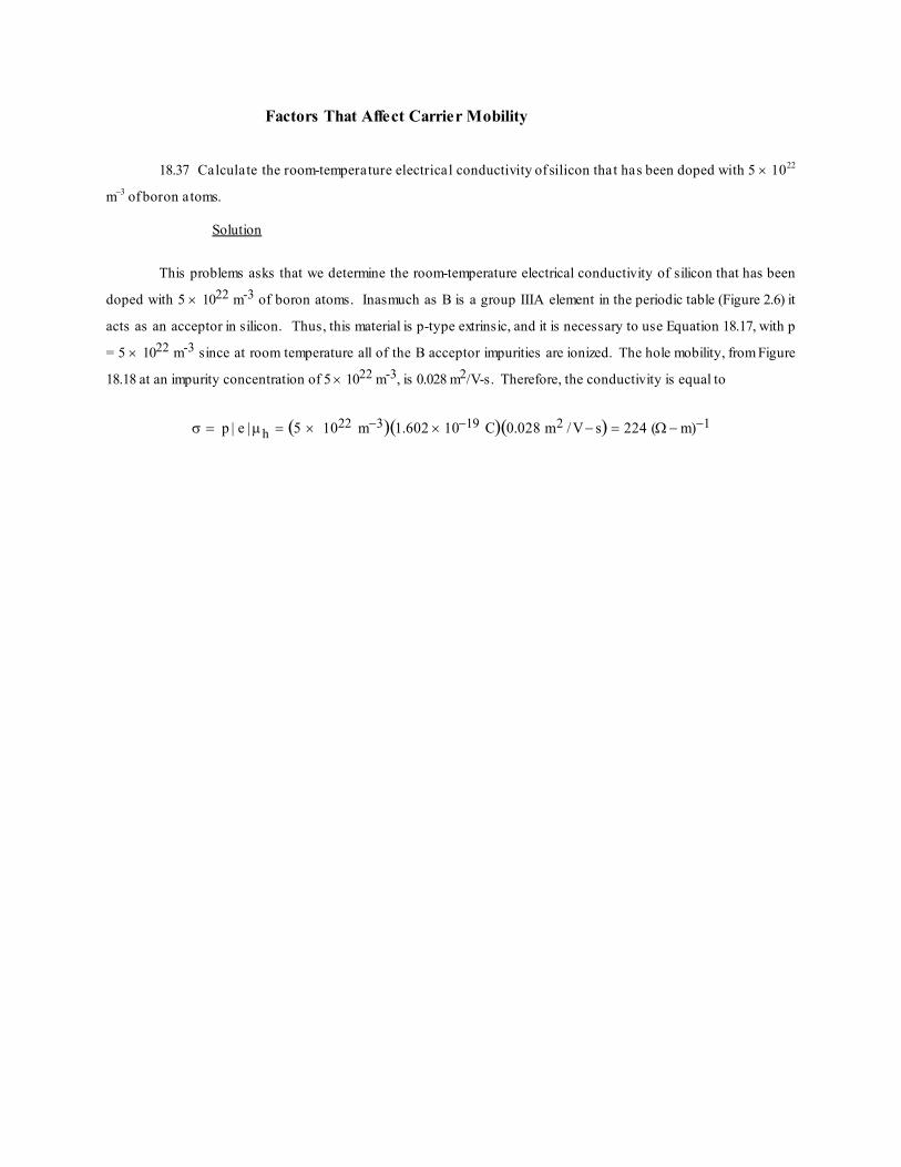
Factors That Affect Carrier Mobility
18.37 Calculate the room-temperat
ure electrical conductivity of silicon that has been doped with 5 ´
10
22
m–
3 of boron atoms. Solution
This problems asks that we determine the room-temperature electrical conductivity of silicon that has been
doped with 5 ´
10
22 m-
3 of boron atoms. In
asmuch as B is a group IIIA element in the periodic table (Figure 2.6) it
acts as an acceptor in silicon. Thus, this material is p-
type extrinsic, and it is necessary to use Equation 18.17, with p
= 5 ´
10
22 m-
3 since at room temperature all of the B acceptor impurities are ionized. The hole mobility, from Figure
18.18 at an impurity concentration of 5 ´
10
22 m-
3
, is 0.028 m
2/V-s. Therefore, the conductivity is equal to
s = p | e | mh = (
5 ´
10
22 m-
3)(
1.
602 ´
10-
19 C)(
0.
028 m
2 /V - s) =
224 (W - m)-
1

18.38 Calculate the room-temperature electrical conduct
ivity of silicon that has been doped with 2 × 10
23
m–
3 of arsenic atoms. Solution
Here we are asked to calculate the room-temperature electrical conductivity of silicon that has been doped
with 2 ´
10
23 m-
3 of arsenic atoms. Inasmuch as As is a group
VA element in the periodic table (Figure 2.6) it acts as
a donor in silicon. Thus, this material is n-
type extrinsic, and it is necessary to use Equation 18.16, with n
= 2 ´
10
23
m-
3 since at room temperature all of the As donor impurities are ionized.
The electron mobility, from Figure 18.18 at
an impurity concentration of 2 ´
10
23 m-
3
, is 0.05 m
2/V-s. Therefore, the conductivity is equal to
s = n | e | me = (
2 ´
10
23 m-
3)(
1.
602 ´
10-
19 C)(
0.
05 m
2 /V - s) =
1600 (W - m)-
1

18.39
Estimate the electrical conductivity, at 125°C, of silicon that has been dop
ed with 10
23 m–
3 of
aluminum atoms. Solution
In this problem we are to estimate the electrical conductivity, at 125°C, of silicon that has been doped with
10
23 m-
3 of aluminum atoms. Inasmuch as Al is a group IIIA element in the periodic table (Figure
2.6) it acts as an
acceptor in silicon. Thus, this material is p-
W\ SH H[WULQVLF DQG LW LV QHFHVVDU\ WR XVH ( TXDWLRQ p in this
expression is 10
23 m-
3
since at 125°C all of the Al acceptor impurities are ionized. The hole mobility is determined
u
sing Figure 18.19b
. From the 10
23 m-
3
impurity concentration curve and at 125°
C (398 K), mh
= 0.017 m
2/V-s.
Therefore, the conductivity is equal to
s = p | e | mh = (
10
23 m-
3)(
1.
602 ´
10-
19 C)(
0.
017 m
2 /V - s) =
272 (W - m)-
1

18.40
Estimate the electrical conductivity, at 85°C,
of silicon that has been doped with 10
20 m–
3 of
phosphorus atoms. Solution
In this problem we are to estimate the electrical conductivity, at 85°C, of silicon that has been doped with
10
20 m-
3 of phosphorus atoms. Inasmuch as P is a group VA element i
n the periodic table (Figure 2.6) it acts as a
donor in silicon. Thus, this material is n-
W\ SH H[WULQVLF DQG LW LV QHFHVVDU\ WR XVH ( TXDWLRQ n in this expression
is 10
20 m-
3
since at 85°C all of the P donor impurities are ionized. The electron mobility is determined using Figure
18.19a
. From the <10
20 m-
3
impurity concentration curve and at 85°
C (358 K,) me
= 0.1 m
2/V-s. Therefore, the
conductivity is equal to
s = n | e | me = (
10
20 m-
3)(
1.
602 ´
10-
19 C)(
0.
1 m
2 /V - s) =
1.
6 (W - m)-
1

The Hall Effect
18.41 Some hypothetical metal is known
to have an electrical resistivity of 4 ´
10-
8 (W-m). Through a
VSHFLP HQ RI WKLV P HWDO WKDW LV P P WKLFN LV SDVVHG D FXUUHQW RI $ ZKHQ D P DJ QHWLF ILHOG RI WHVOD LV
simultaneously imposed in a direction perpendicular to that of the current, a Hall voltage of -
1.26 ´
10-
7 V is
measured. Compute (a) the electron mobility for this metal, and (b) the number of free electrons per cubic meter. Solution
(a) This portion of the problem calls for us to determine the electron mobility for some hypothetical metal
using the Hall effect. This metal has an electrical resistivity of 4 ´
10-
8 (W-
m), while the specimen thickness is 25 mm,
Ix
= 30 A and Bz
WHVOD XQGHU WKHVH FLUFXP VWDQFHV D + DOO YROWDJ H RI –
1.26 ´
10-
7 V is measured. It is first
necessary to convert resistivity to conductivity (Equation 18.4). Thus
s =
1
r=
1
4 ´
10-
8 (W - m)=
2.5 ´
10
7 (W - m)
-1
7KH HOHFWURQ P RELOLW\ P D\ EH GHWHUP LQHG XVLQJ ( TXDWLRQ E DQG XSRQ LQFRUSRUDWLRQ RI ( TXDWLRQ ZH KDYH
me = RH s
= VH d s
I xBz
=-
1.
26 ´
10-
7 V( )(
25 ´
10-
3 m)
2.
5 ´
10
7 (W - m)-
1[ ]
(
30 A)(
0.
75 tesla)
=
0.0035 m
2/V - s
(b) Now we are to calculate the num
ber of free electrons per cubic meter. From Equation 18.8 we have
n =s
| e | me
=
2.
5 ´
10
7 (W - m)-
1
(
1.
602 ´
10-
19 C)(
0.
0035 m
2/V - s)
=
4.46 ´
10
28 m
-3

18.42
Some metal alloy is known to have electrical conductivity and electron mobility values of 1.5 ´
10
7
(W-m)-
1
and 0.0020 m
2/V-
s, respectively. Through a specimen of this alloy that is 35 mm thick is passed a current of
45 A. What magnetic field would need to be imposed to yield a Hall voltage of -
1.0 ´
10-
7 V? Solution
In this problem we are asked to determine the magnetic field required to produce a Hall voltage of -
1.0 ´
10-
7
V, given that s
= 1.5 ´
10
7 (W-m)-
1, me
= 0.0020 m
2/V-s, Ix
= 45 A, and d
= 35 mm. Combining Equations 18.18 and
18.20b, and after solving for Bz, we get
Bz =VH d
I xRH
=VH sd
I xme
= -
1.
0 ´
10-
7 V( )
1.
5 ´
10
7 (W - m)-
1[ ](
35 ´
10-
3 m)
(
45 A)(
0.
0020 m
2 /V - s)
= 0.58 tesla

Semiconducting Devices
18.43 Briefly describe electron and hole motions in a p–n junction for forward and reverse biases; then
explain how these lead to rectification.
The explanations called for are found in
Section 18.15.

18.44
How is the energy in the reaction described by Equation 18.21 dissipated? Solution
The energy generated by the electron-
hole annihilation reaction, Equation 18.21, is dissipated as heat.

18.45 What are the two functions that a transistor may perform in an electronic circuit? Solution
In an electronic circuit, a transistor may be used to (1) amplify an electrical signal, and (2) act as a switching
device in computers.

18.46 Cite the differences in operation and application for junction transistors and MOSFETs.
The differences in operation and application for junction transistors and MOSFETs are described in Section
18.15.

Conduction in Ionic Materials
18.47
We noted in Section 12.5 (Figure 12.22) that in FeO (wüstite), the iron ions can exist in both Fe
2+
and Fe
3+ states. The number of each of these ion types depends on temperature and the ambient oxygen pressure.
Furthermore, we also noted that in order to retain electroneutrality, one Fe
2+ vacancy will be created for every two
Fe
3+ ions that are formed; consequently, in order to reflect the existence of these vacancies the formula for wüstite
is often represented as Fe
(1 – x) O where x is some small fraction less than unity.
In this nonstoichiometric Fe
(1 – x) O material, conduction is electronic, and, in fact, it behaves as a p-type
semiconductor. That is, the Fe
3+ ions act as electron acceptors, and it is relatively easy to excite an electron from
the valence band into an Fe
3+ acceptor state, with the formation of a hole. Determine the electrical conductivity of
a specimen of wüstite that has a hole mobility of 1.0 × 10–
5 m
2/V-
s and for which the value of x is 0.060. Assume that
the acceptor states are saturated (i.e., one hole exists for every Fe
3+ ion). Wüstite has the sodium chloride crystal
structure with a unit cell edge length of 0.437 nm. Solution
We are asked in this problem to determine the electrical conductivity for the nonstoichiometric Fe
(1 - x)O,
given x
= 0.060 and that the hole mobility is 1.0 ´
10-
5 m
2/V-s. It is first necessary to compute the number of
vacancies per cubic meter for this material. For this determination let us use as our basis 10 unit cells. For the sodium
chloride crystal structure there are four cations and four anions per unit cell. Thus, in ten unit cells of FeO there will
normally be forty O
2- and forty Fe
2+ ions. However, when x
= 0.06, (0.06)(40) = 2.4 of the Fe
2+ sites will be vacant.
(Furthermore, there will be 4.8 Fe
3+ ions in these ten unit cells inasmuch as two Fe
3+ ions are created for every
vacancy). Therefore, each unit cell will, on the average contain 0.24 vacancies. Now, the number of vacancies per
cubic meter is just the number of vacancies per unit cell divided by the unit cell volume; this volume is just the unit
cell edge length (0.437 nm) cubed. Thus
# vacancies
m
3=
0.
24 vacancies /unit cell
(
0.
437 ´
10-
9 m)
3
=
2.88 ´
10
27 vacancies/m
3
Inasmuch as it is assumed that the vacancies are saturated, the number of holes (p
) is also 2.88 ´
10
27 m-
3. It is now
possible, using Equation 18.1
7, to compute the electrical conductivity of this material as
s = p | e |mh
= (
2.88 ´
10
27 m
-3)(
1.602 ´
10
-19 C)(
1.0 ´
10
-5 m
2/V - s) =
4613 (W - m)
-1

18.48
At temperatures between 775°
C (1048 K) and 1100°
C (1373 K), the activation energy and
preexponential for the diffusion coefficient of Fe
2+
in FeO are 102,000 J/mol and 7.3 ´
10-
8 m
2/s, respectively.
Compute the mobility for an Fe
2+
ion at 1000°
C (1273 K). Solution
For this problem, we are given, for FeO, the activation energy (102,000 J/mol) and preexponential (7.3 ´
10-
8
m
2/s) for the diffusion coefficient of Fe
2+ and are asked to compute the mobility for a Fe
2+
ion at 1273 K. The
mobility, mFe
2+
P D\ EH FRP SXWHG XVLQJ ( TXDWLRQ KRZHYHU WKLV H[SUHVVLRQ DOVR LQFOXGHV WKH GLIIXVLRQ
coefficient D Fe
2+
, which is determined using Equation 5.8 as
DFe
2+ = D
0 exp -Qd
RT
æ
è ç
ö
ø ÷
= (
7.3 ´
10
-8 m
2/s) exp -
102,
000 J /mol
(
8.
31 J/mol - K)(
1273 K)
é
ë ê
ù
û ú
=
4.74 ´
10
-12 m
2/s
Now solving for mFe
2+ yields
mFe
2+ =n
Fe
2+ eDFe
2+
kT
= (
2)(
1.
602 ´
10-
19 C /atom)(
4.
74 ´
10-
12 m
2 /s)
(
1.
38 ´
10-
23J/atom- K) (
1273 K)
=
8.64 ´
10
-11 m
2/V - s
(Note: the value of nFe
2+ is two, inasmuch as two electrons are involved in the ionization of Fe to Fe
2+.)

Capacitance
18.49 A parallel-plate capacitor using a dielectric material having an er
of 2.5 has a plate spacing of 1
mm (0.04 in.). If another material having a dielectric constant of 4.0 is used and the capacitance is to be
unchanged, what must be the new spacing between the plates? Solution
We want to compute the plate spacing of a parallel-plate capacitor as the dielectric constant is increased
form 2.5 to 4.0, while maintaining the capacitance constant. Combining Equations 18.26 and 18.27 yields
C =eA
l=
ere
0 A
l
Now, let us use the subscripts 1 and 2 to denote the initial and final states, respectively. Since C
1 = C
2, then
er
1e
0 A
l
1
= er
2 e
0 A
l
2
And, solving for l
2
l
2 = er
2l
1
er
1
= (
4.
0)(
1 mm)
2.
5=
1.6 mm

18.50 A parallel-
plate capacitor with dimensions of 100 mm by 25 mm and a plate separation of 3 mm
must have a minimum capaci
tance of 38 pF (3.8 ´
10-
11
F) when an ac potential of 500 V is applied at a frequency
of 1 MHz. Which of those materials listed in Table 18.5 are possible candidates? Why? Solution
This problem asks for us to ascertain which of the materials listed
in Table 18.5 are candidates for a parallel-
plate capacitor that has dimensions of 100 mm by 25 mm, a plate separation of 3 mm so as to have a minimum
capacitance of 3.8 ´
10-
11
F, when an ac potential of 500 V is applied at 1 MHz. Upon combining Equation
s 18.26 and
18.27 and solving for the dielectric constant er we get
er = e
e
0
= lC
e
0 A
= (
3 ´
10-
3 m)(
3.
8 ´
10-
11F)
(
8.
85 ´
10-
12 F /m)(
100 ´
10-
3 m)(
25 ´
10-
3 m)
= 5.15
Thus, the minimum value of er
to achieve the desired capacitance is 5.15 at 1 MHz. Of those materials listed in the
table, titanate ceramics, mica, steatite, soda-lime glass, and porcelain are candidates.

18.51 Consider a parallel-
plate capacitor having an area of 2500 mm
2
and a plate separation of 2 mm,
and with a material of dielectric constant 4.0 positioned between the plates. (a) What is the capacitance of this
capacitor? (b)
Compute the electric field that must be applied for 8.0 ´
10-
9 C to be stored on each plate. Solution
In this problem we are given, for a parallel-
plate capacitor, its area (2500 mm
2), the plate se
paration (2 mm),
and that a material having an er
of 4.0 is positioned between the plates.
(a) We are first asked to compute the capacitance. Combining Equations 18.26 and 18.27, and solving for C
yields
C = eA
l=
ere
0 A
l
= (
4.
0)(
8.
85 ´
10-
12 F /m)(
2500 mm
2)(
1 m
2 /
10
6 mm
2)
2 ´
10-
3 m
= 4.43 ´
10-
11
F = 44.3 pF
(b) Now we are asked to compute the electric field that must be applied in order that 8 ´
10-
9 C be stored on
each plate. First we need to solve for V
in Equation 18.24 as
V = Q
C=
8 ´
10-
9 C
4.
43 ´
10-
11 F=
181 V
The electric field E may
QRZ EH GHWHUP LQHG XVLQJ ( TXDWLRQ WKXV
E = V
l=
181 V
2 ´
10-
3 m=
9.1 ´
10
4 V/m

18.52 In your own words, explain the mechanism by which charge storing capacity is increased by the
insertion of a dielectric material within the plates of a capacitor.
This explana
tion is found in Section 18.19.

Field Vectors and Polarization
Types of Polarization
18.53 For NaCl, the ionic radii for Na+ and Cl-
ions are 0.102 and 0.181 nm, respectively. If an externally
applied electric field produces a 5% expansion of the lattice, compute the dipole moment for each Na+–Cl- pair.
Assume that this material is completely unpolarized in the absence of an electric field. Solution
Shown below are the relative positions of Na+ and Cl- ions, without and with an electric field present.
Now,
d = rNa+ + r
Cl- =
0.102 nm +
0.181 nm =
0.283 nm
and
Dd =
0.05 d =
(0.05)(0.283 nm) =
0.0142 nm =
1.42 ´
10
-11 m
From Equation 18.28, the dipole moment, p, is just
p = q Dd
= (
1.602 ´
10
-19 C)(
1.42 ´
10
-11 m)
= 2.26 ´
10-
30 C-m

18.54 The polarization P of a dielectric material positioned within a parallel-
plate capacitor is to be 1.0
´
10-
6 C/m
2.
(a)
What must be the dielectric constant if an electric field of 5 ´
10
4 V/m is applied?
(b) What will be the dielectric displacement D? Solution
(a) In order to solve for the dielectric con
stant in this problem, we must employ Equation 18.32, in which the
polarization and the electric field are given. Solving for er from this expression gives
er = P
e
0E+
1
=
1.
0 ´
10-
6 C /m
2
(
8.
85 ´
10-
12 F /m)(
5 ´
10
4 V /m)+
1
= 3.26
(b) The dielectric displacement may be
determined using Equation 18.31, as
D = e
0E + P
= (
8.85 ´
10
-12 F/m)(
5 ´
10
4 V/m) +
1.0 ´
10
-6 C/m
2
= 1.44 ´
10-
6 C/m
2

18.55
A charge of 3.5 ´
10-
11 C is to be stored on each plate of a parallel-plate capacitor having an area of
160 mm
2
(0.25 in.
2) and a plate separ
ation of 3.5 mm (0.14 in.).
(a)
What voltage is required if a material having a dielectric constant of 5.0 is positioned within the
plates?
(b) What voltage would be required if a vacuum were used?
(c) What are the capacitances for parts (a) and (b)?
(d) Compute the dielectric displacement for part (a).
(e) Compute the polarization for part (a). Solution
(a) We want to solve for the voltage when Q
= 3.5 ´
10-
11 C, A
= 160 mm
2, l
= 3.5 mm, and er
= 5.0.
Combining Equations 18.24, 18.26, and 18.27 yields
C =Q
V= e
A
l= ere
0A
l
Or
Q
V= ere
0A
l
And, solving for V, and incorporating values provided in the problem statement, leads to
V = Q l
ere
0 A
= (
3.
5 ´
10-
11 C)(
3.
5 ´
10-
3 m)
(
5.
0)(
8.
85 ´
10-
12 F /m)(
160 mm
2)(
1 m
2 /
10
6 mm
2)
= 17.3 V
(b) For this same capacitor, if a vacuum is used
V = Q l
e
0 A
= (
3.
5 ´
10-
11 C)(
3.
5 ´
10-
3 m)
(
8.
85 ´
10-
12 F /m)(
160 ´
10-
6 m
2)

= 86.5 V
(c) The capacitance for part (a) is just
C = Q
V=
3.
5 ´
10-
11 C
17.
3 V=
2.0 ´
10
-12 F
While for part (b)
C = Q
V=
3.
5 ´
10-
11 C
86.
5 V=
4.0 ´
10
-13 F
(d) The dielectric displacement may be computed by combining Equations 18
.31, 18.32 and 18.6, as
D = e
0E + P = e
0E + e
0(er -
1)E = e
0erE =e
0erV
l
And incorporating values for er and l provided in the problem statement, as well as the value of V computed in part
(a)
D = (
8.
85 ´
10-
12 F /m) (
5.
0)(
17.
3 V)
3.
5 ´
10-
3 m
= 2.2 ´
10-
7 C/m
2
(e) The polarization is determined usin
g Equations 18.32 and 18.6 as
P = e
0(er -
1)E = e
0(er -
1)V
l
= (
8.
85 ´
10-
12 F /m) (
5.
0 -
1)(
17.
3 V)
3.
5 ´
10-
3 m
= 1.75 ´
10-
7 C/m
2

18.56 (a) For each of the three types of polarization, briefly describe the mechanism by which dipoles are
induced and/or oriented by the action of an applied electric field. (b) For solid lead titanate (PbTiO
3), gaseous
neon, diamond, solid KCl, and liquid NH
3 what kind(s) of polarization is (are) possible? Why? Solution
(a) For electronic polarization, the electric field causes a net displacement of the center of the negatively
charged electron cloud relative to the positive nucleus. With ionic polarization, the cations and anions are displaced
in opposite directions as a result of the application of an electric field. Orientation polarization is found in substances
that possess permanent dipole moments; these dipole moments become aligned in the direction of the electric field.
(b) Electronic, ionic, and orientation polarizations would be observed in lead titanate. The lead, titanium,
and oxygen would undoubtedly be largely ionic in character. Furthermore, orientation polarization is also possible
inasmuch as permanent dipole moments may be induced in the same manner as for BaTiO
3
as shown in Figure 18.35.
Only electronic polarization is to be found in gaseous neon; being an inert gas, its atoms will not be ionized
nor possess permanent dipole moments.
Only electronic polarization is to be found in solid diamond; this material does not have molecules with
permanent dipole moments, nor is it an ionic material.
Both electronic and ionic polarizations will be found in solid KCl, since it is strongly ionic. In all probability,
no permanent dipole moments will be found in this material.
Both electronic and orientation polarizations are found in liquid NH
3. The NH
3 molecules have permanent
dipole moments that are easily oriented in the liquid state.

18.57 (a) Compute the magnitude of the dipole moment associated with each unit cell of BaTiO
3, as
illustrated in Figure 18.35.
(b) Compute the maximum polarization that is possible for this material. Solution
(a) This portion of the problem asks that we compute the magnitude of the dipole moment associated with
each unit cell of BaTiO
3
, which is illustrated in Figure 18.35. The dipole moment p
is defined by Equation 18.28 as p =
qd in which q is the magnitude of each dipole charge, and d is the distance of separation between the charges. Each
Ti
4+ ion has four units of charge associated with it, and thus q
= (4)(1.602 ´
10-
19
C) = 6.41 ´
10-
1
9 C. Furthermore, d
is the distance the Ti
4+
ion has been displaced from the center of the unit cell, which is just 0.006 nm + 0.006 nm =
0.012 nm [Figure 18.35(b)]. Hence
p = qd = (
6.41 ´
10
-19 C)(
0.012 ´
10 -
9 m)
= 7.69 ´
10-
30 C-m
(b) Now it becomes necessary to compute the maximum polarization that is possible for this material. The
maximum polarization will exist when the dipole moments of all unit cells are aligned in the same direction.
Furthermore, it is computed by dividing the above value of p by the volume of each unit cell, which is equal to the
product of three unit cell edge lengths, as shown in Figure 18.35. Thus
P = p
VC
=
7.
69 ´
10-
30 C - m
(
0.
403 ´
10-
9 m)(
0.
398 ´
10-
9 m)(
0.
398 ´
10-
9 m)
= 0.121 C/m
2

Frequency Dependence of the Dielectric Constant
18.58 The dielectric constant for a soda–lime glass measured at very high frequencies (on the order of
10
15
Hz) is approximately 2.3. What fraction of the dielectric constant at relatively low frequencies (1 MHz) is
attributed to ionic polarization? Neglect any orientation polarization contributions. Solution
For this soda-lime glass, in order to compute the fraction of the dielectric constant at low frequencies that is
attributed to ionic polarization, we must determine the er within this low-frequency regime; such is tabulated in Table
18.5, and at 1 MHz its value is 6.9. Thus, this fraction is just
fraction = er (low) - er (high)
er (low)
=
6.
9 -
2.
3
6.
9=
0.67
Ferroelectricity
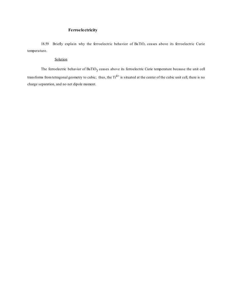
18.59 Briefly explain why the ferroelectric behavior of BaTiO
3 ceases above its ferroelectric Curie
temperature. Solution
The ferroelectric behavior of BaTiO
3 ceases above its ferroelectric Curie temperature because the unit cell
transforms from tetragonal geometry to cubic; thus, the Ti
4+ is situated at the center of the cubic unit cell, there is no
charge separation, and no net dipole moment.

DESIGN PROBLEMS
Electrical Resistivity of Metals
18.D1
A 95 wt% Pt-
5 wt% Ni alloy is known to have an electrical resistivity of 2.35 ´
10-
7 W-m at room
temperature (25°C). Calculate the composition of a platinum-nickel alloy that gives a room-temperature
resistivity of 1.75 ´
10-
7 W-m. The room-temperature resistivity of pure platinum may be determined from the data
LQ 7DEOH DVVXP H WKDW SODWLQXP DQG QLFNHO IRUP D VROLG VROXWLRQ Solution
This problem asks that we calculate the composition of a platinum-nickel alloy that has a room temperature
resistivity of 1.75 ´
10-
7 W-
m. The first thing to do is, using the 95 Pt-
5 Ni resistivity data, determine the impurity
contribution, and, from this result, calculate the constant A
in Equation 18.11. Thus,
rtotal =
2.35 ´
10
-7 (W - m) = ri + rt
From Table 18.1, for pure platinum, and using Equation 18.4
rt =
1
s=
1
0.
94 ´
10
7 (W - m)-
1=
1.064 ´
10
-7 (W - m)
Thus, for the 95 Pt-
5 Ni alloy
ri = rtotal - rt =
2.35 ´
10
-7 -
1.064 ´
10
-7
= 1.286 ´
10-
7 (W-m)
In the problem statement, the impurity (i.e., nickel) concentration is expressed in weight percent. However, Equation
18.11 calls for concentration in atom fraction (i.e., atom percent divided by 100). Consequently, conversion from
weight percent to atom fraction is necessary. (Note: we now choose to denote the atom fraction of nickel as
cNi' ,
and the weight percents of Ni and Pt by CNi and CPt, respectively.) Using these notations, this conversion may be
accomplished by using a modified form of Equa
tion 4.6a as
cNi' =
CNi'
100=
CNi APt
CNi APt + CPt ANi

Here ANi and APt
denote the atomic weights of nickel and platinum (which values are 58.69 and 195.08 g/mol,
respectively). Thus
cNi' =
(
5 wt%)(
195.
08 g /mol)
(
5 wt%)(
195.
08 g /mol) + (
95 wt%)(
58.
69 g /mol)
= 0.15
Now, solving for A
in Equation 18.11
A = ri
cNi'
1 - cNi'æ
è ç
ö ø ÷
=
1.
286 ´
10-
7 (W - m)
(
0.
15)(
1 -
0.
15)=
1.01 ´
10
-6 (W - m)
Now it is possible to compute the
cNi'
to give a room temperature resistivity of 1.75 ´
10-
7 W-m. Again, we must
determine ri as
ri = rtotal - rt
=
1.75 ´
10
-7 -
1.286 ´
10
-7 =
4.64 ´
10
-8 (W - m)
If Equation 18.11 is expanded, then
ri = AcNi' - A c
Ni'
2
Or, rearranging this equation, we have
A cNi'
2
- AcNi' + ri =
0
Now, solving for
cNi' (using the quadratic equation solution)

cNi' =
A ± A
2 -
4 Ari
2A
Again, from the above
A
= 1.01 ´
10-
6 (W-m)
ri
= 4.64 ´
10-
8 (W-m)
which leads to
cNi' =
1.
01 ´
10-
6 ± (
1.
01 ´
10-
6)
2 - (
4)(
1.
01 ´
10-
6)(
4.
64 ´
10-
8)
(
2)(
1.
01 ´
10-
6)
And, taking the negative root,
cNi' =
0.0483
Or, in terms of atom percent,
CNi
=
100 cNi
= (
100)(
0.
0483) =
4.
83 at%
While the concentration of platinum is
CPt
=
100 - CNi
=
100 .
00 -
4.
83 =
95.
17 at%
Now, converting this composition to weight percent Ni, requires that we use Equation 4.7a as
CNi = CNi
' ANi
CNi' ANi + CPt
' APT
´
100
= (
4.
83 at%)(
58.
69 g /mol)
(
4.
83 at%)(
58.
69 g /mol) + (
95.
17 at%)(
195.
08 g /mol)´
100
= 1.50 wt%

18.D2
Using information contained in Figures 18.8 and 18.38, determine the electrical conductivity of an
80 wt% Cu-
20 wt% Zn alloy at -
150°C (-
240°F). Solution
This problem asks that we determine the electrical conductivity of an 80 wt% Cu-
20 wt% Zn alloy at
–
150°
C using information contained in Figures 18.8 and 18.38. In order to solve this problem it is necessary to
employ Equation 18.9 which is of the form
rtotal = rt + ri
since it is assumed that the alloy is undeformed. Let us first determine the value of ri
at room temperature (25°C)
which value will be independent of temperature. From Figure 18.8, at 25°C and for pure Cu, rt
(25) = 1.75 ´
10-
8 W-m.
Now, since it is assumed that the curve in Figure 18.38 was generated also at room temperature, we may take r as
rtotal
(25) at 80 wt% Cu-
20 wt% Zn which has a value of 5.3 ´
10-
8 W-m. Thus
ri = rtotal
(25) - rt
(25)
=
5.3 ´
10
-8 W - m -
1.75 ´
10
-8 W - m =
3.55 ´
10
-8 W - m
Finally, we may determine the resistivity at –
150°C, rtotal(–
150), by taking the resistivity of pure Cu at –
150°C from
Figure 18.8, which gives us rt(–
150) = 0.55 ´
10-
8 W-m. Therefore
rtotal (-
150) = ri + rt (-
150)
=
3.55 ´
10
-8 W - m +
0.55 ´
10
-8 W - m =
4.10 ´
10
-8 W - m
And, using Equation 18.4 the conductivity is calculated as
s =
1
r=
1
4.
10 ´
10-
8 W - m=
2.44 ´
10
7 (W - m)
-1

18.D3 Is it possible to alloy co
pper with nickel to achieve a minimum tensile strength of 375 MPa (54,400
psi) and yet maintain an electrical conductivity of 2.5 ´
10
6 (W-m)-
1? If not, why? If so, what concentration of
nickel is required? You may want to consult Figure 7.16a. Solution
To solve this problem, we want to consult Figures 7.16a
and 18.9 in order to determine the Ni concentration
ranges over which the tensile strength is greater than 375 MPa (54,500 psi) and the conductivity exceeds 2.5 ´
10
6
(W-m)-
1.
From Figure 7.16a ,
a Ni concentration greater than about 30 wt% is necessary for a tensile strength in excess
of 375 MPa. In Figure 18.9 is plotted the resistivity versus the Ni content. Since conductivity is the reciprocal of
resistivity, the resistivity must be less tha
n 40 ´
10-
8 W-m--i.e.,
1
2.
5 ´
10
6 (W - m)-
1. According to the figure, this
will be the case for Ni concentrations less than 32.5 wt%.
Hence, it is possible to prepare an alloy meeting the criteria. The concentration of Ni would have to lie
between about 30 and 3
2.5 wt%.

Extrinsic Semiconduction
Factors That Affect Carrier Mobility
18.D4 Specify an acceptor impurity type and concentration (in weight percent) that will produce a p-type
silicon material having a room temperature electrical conductivity of 50 (W-m)-
1. Solution
First of all, those elements which, when added to silicon render it p-type, lie one group to the left of silicon
LQ WKH SHULRGLF WDEOH WKHVH LQFOXGH WKH J URXS ,,,$ HOHP HQWV ) LJ XUH --i.e., boron, aluminum, gallium, and indium.
Since this material is extrinsic and p-type, p >> n, and the electrical conductivity is a function of the hole
concentration according to Equation 18.17. Also, the number of holes is about equal to the number of acceptor
impurities, Na. That is
p ~ Na
F
rom Equation 18.17, the conductivity is a function of both the hole concentration (p) and the hole mobility (mh).
Furthermore, the room-
temperature hole mobility is dependent on impurity concentration (Figure 18.18). One way to
solve this problem is to use an iterative approach—i.e., assume some acceptor impurity concentration (which will also
equal the value of p
), then determine a "calculated" hole mobility from Equation 18.17—i.e.,
mh =s
p | e |
and, finally, compare this mobility with the "measured" value from Figure 18.18, taken at the assumed p (i.e., Na)
value.
Let us begin by assuming that Na
= 10
22 m-
3. Thus, the "calculated" mobility value is
mh =s
p | e |=
50 (W - m)-
1
(
10
22 m-
3)(
1.
602 ´
10-
19 C)=
0.
0312 m
2 /V - s
From Figure 18.18, at an impurity concentration of 10
22 m-
3
the "measured" hole mobility is 0.0362 m
2/V-s, which is
slightly higher than the "calculated" value.
For our next
choice, let us assume a lower impurity concentration, say 5 ´
10
21 m-
3. At this lower
concentration there will be an increase of both "calculated" and "measured" electron mobilities. The "calculated"
value is just
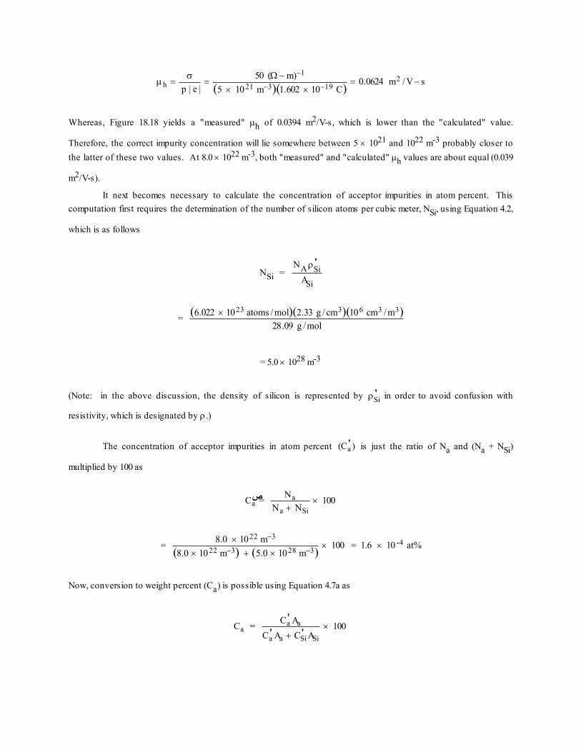
mh =s
p | e |=
50 (W - m)-
1
(
5 ´
10
21 m-
3)(
1.
602 ´
10-
19 C)=
0.
0624 m
2 /V - s
Whereas, Figu
re 18.18 yields a "measured" mh
of 0.0394 m
2/V-s, which is lower than the "calculated" value.
Therefore, the correct impurity concentration will lie somewhere between 5 ´
10
21
and 10
22 m-
3 probably closer to
the latter of these two values. At 8.0 ´
10
22 m-
3, both "measured" and "calculated" mh
values are about equal (0.039
m
2/V-s).
It next becomes necessary to calculate the concentration of acceptor impurities in atom percent. This
computation first requires the determination of the number of silicon atoms per cubic meter, NSi, usi
ng Equation 4.2,
which is as follows
NSi = NA rSi
'
ASi
= (
6.
022 ´
10
23 atoms /mol)(
2.
33 g /cm
3)(
10
6 cm
3 /m
3)
28.
09 g /mol
= 5.0 ´
10
28 m-
3
(Note: in the above discussion, the density of silicon is represented by
rSi' in order to avoid confusion with
resistivity, which is designated by r.)
The concentration of acceptor impurities in atom percent
(Ca' ) is just the ratio of Na and (Na + NSi)
multiplied by 100 as
Ca
= Na
Na + NSi
´
100
=
8.
0 ´
10
22 m-
3
(
8.
0 ´
10
22 m-
3) + (
5.
0 ´
10
28 m-
3)´
100 =
1.6 ´
10
-4 at%
Now, conversion to weight percent (Ca) is possible using E
quation 4.7a as
Ca = Ca
' Aa
Ca' Aa + CSi
' ASi
´
100

where Aa and ASi are the atomic weights of the acceptor and silicon, respectively. Thus, the concentration in weight
percent will depend on the particular acceptor type. For example, for boron
CB = CB
' AB
CB' AB + CSi
' ASi
´
100
= (
1.
6 ´
10-
4 at%) (
10.
81 g /mol)
(
1.
6 ´
10-
4 at%) (
10.
81 g/mol) + (
99.
99984 at%)(
28.
09 g/mol)´
100
= 6.16 ´
10-
5 wt%
Similar calculations may be carried out for the other possible acceptor impurities which yield
CAl =
1.54 ´
10
-4 wt%
CGa =
3.97 ´
10
-4 wt%
CIn =
6.54 ´
10
-4 wt%

18.D5 One integrated circuit design calls for diffusing boron into very high purity silicon at an elevated
temperature. It is necessary that at a distance 0.2 mm from the surface of the silicon wafer, the room-temperature
electrical conductivity be 1.2 ´
10
3 (W-m)-
1. The concentration of B at the surface of the Si is maintained at a
constant level of 1.0 ´
10
25 m-
3; furthermore, it is assumed that the concentration of B in the original Si material is
negligible, and that at room temperature the boron atoms are saturated. Specify the temperature at which this
diffusion heat treatment is to take place if the treatment time is to be one hour. The diffusion coefficient for the
diffusion of B in Si is a function of temperature as
D(m
2/s) =
2.4 ´
10
-4 exp -
347 kJ/mol
RT
æ
è ç
ö
ø ÷
Solution
This problem asks for us to determine the temperature at which boron is to be diffused into high-purity
silicon in order to achieve a room-
temperature electrical conductivity of 1.2 ´
10
3 (W-m)-
1
at a distance 0.2 mm from
the surface if the B concentration at the surface is maintain
ed at 1.0 ´
10
25 m-
3. It is first necessary for us to compute
the hole concentration (since B is an acceptor in Si) at this 0.2 mm location.
From Equation 18.17, the conductivity is a function of both the hole concentration (p) and the hole mobility
(mh). Furthermore, the room-
temperature hole mobility is dependent on impurity concentration (Figure 18.18). One
way to solve this problem is to use an iterative approach—i.e., assume some boron concentration, NB (which will
also equal the value of p), then
determine a "calculated" hole mobility from Equation 18.17—i.e.,
mh =s
p | e |
and then compare this mobility with the "measured" value from Figure 18.18, taken at the assumed p (i.e., NB).
Let us begin by assuming that NB
= 10
23 m-
3. Thus, the "calculated" mobility value is
mh =s
p | e |=
1.
2 ´
10
3 (W - m)-
1
(
10
23 m-
3)(
1.
602 ´
10-
19 C)=
0.
075 m
2 /V - s
From Figure 18.18, at an impurity concentration of 10
23 m-
3
the "measured" hole mobility is 0.024 m
2/V-s, which is
lower than the "calculated" value.
For our next choice, let us assume a higher b
oron concentration, say 10
24 m-
3. At this higher concentration
there will be a decrease of both "calculated" and "measured" hole mobilities. The "calculated" value is just
mh =s
p | e |=
1.
2 ´
10
3 (W - m)-
1
(
10
24 m-
3)(
1.
602 ´
10-
19 C)=
0.
0075 m
2 /V - s

Whereas, Figure 18.18 yields a "measured" mh
of 0.01 m
2/V-s, which is lower than the "calculated" value. Therefore,
the correct impurity concentration will lie somewhere between 10
23
and 10
24 m-
3
. At 6.0 ´
10
23 m-
3, "measured" and
"calculated" values are about equal (0.0125 m
2/V-s).
With regard to diffusion, the problem is one involving the nonsteady-state diffusion of B into the Si,
wherein we have to solve for temperature. Temperature is incorporated into the diffusion coefficient expression
given in the problem. But we must first employ the solution to Fick's second law for constant surface composition
ERXQGDU\ FRQGLWLRQV ( TXDWLRQ LQ WKLV H[SUHVVLRQ C
0 is taken to be zero inasmuch as the problem stipulates that
the initial boron concentration may be neglected. Thus,
Cx - C
0
Cs - C
0
=
1 - erfx
2 Dt
æ
è ç ç
ö
ø ÷ ÷
6.
0 ´
10
23m-
3 -
0
1.
0 ´
10
25 m-
3 -
0=
1 - erfx
2 Dt
æ
è ç ç
ö
ø ÷ ÷
which reduces to
0.9400 = erfx
2 Dt
æ
è ç ç
ö
ø ÷ ÷
In order to solve this expression for a value
x
2 Dt
of it is necessary to interpolate using data in Table 5.1. Thus
z erf(z)
1.3
0.9340
z
0.9400
1.4
0.9523
z -
1.
3
1.
4 -
1.
3=
0.
9400 -
0.
9340
0.
9523 -
0.
9340
From which, z
ZKLFK LV WR VD\

1.3328 =x
2 Dt
Inasmuch as there are 3600 s/h (= t) and x
= 0.2 m
m (= 2 ´
10-
7 m) the above equation becomes
1.3328 =
2 ´
10-
7 m
2 (D)(
3600 s)
which, when solving for the value of D, leads to
D =
1
3600 s
2 ´
10-
7 m
(
2)(
1.
3328 )
é
ë ê
ù
û ú
2
=
1.
56 ´
10-
18 m
2 /s
Now, equating this value to the expression for D given in the problem gives
D =
1.56 ´
10
-18 m
2/s = (
2.4 ´
10
-4) exp -
347,
000 J/mol
(
8.
31 J/mol - K)(T)
é
ë ê
ù
û ú
To solve for T, let us take the natural logarithms of both sides of the above equation; this leads to
ln(
1.
56 ´
10-
18) = ln(
2.
4 ´
10-
4 ) -
347,
000
8.
31T
-
41.
002 = -
8.
335 -
4.
176 ´
10
4
T
which yields a value for T
of 1278 K (1005°C).

Conduction in Ionic Materials
18.D6
Problem 18.47 noted that FeO (wüstite) may behave as a semiconductor by virtue of the
transformation of Fe
2+ to Fe
3+ and the creation of Fe
2+ vacancies; the maintenance of electroneutrality requires
that for every two Fe
3+ ions, one vacancy is formed. The existence of these vacancies is reflected in the chemical
formula of this nonstoichiometric wüstite as Fe
(1 – x)O, where x is a small number having a value less than unity.
The degree of nonstoichiometry (i.e., the value of x) may be varied by changing temperature and oxygen partial
pressure. Compute the value of x that is required to produce an Fe
(1 – x)O material having a p-type electrical
conductivity of 2000 (W-m)-
1
DVVXP H WKDW WKH KROH P RELOLW\ LV ´
10-
5 m
2/V-s, the crystal structure for FeO is
sodium chloride (with a
unit cell edge length of 0.437 nm), and that the acceptor states are saturated. Solution
This problem asks, for the nonstoichiometric Fe
(1 - x)
O, given the electrical conductivity [2000 (W-m)-
1] and
hole mobility (1.0 ´
10-
5 m
2/V-s) that we determine the value of x. It is first necessary to compute the number of
holes per unit volume (p
) using Equation 18.17. Thus
p =s
| e | mh
=
2000 (W - m)-
1
(
1.
602 ´
10-
19 C)(
1.
0 ´
10-
5 m
2 /V - s)=
1.25 ´
10
27 holes/m
3
Inasmuch as it is assumed that the acceptor states are saturated, the number of vacanci
es is also 1.25 ´
10
27 m-
3.
Next, it is possible to compute the number of vacancies per unit cell by taking the product of the number of vacancies
per cubic meter times the volume of a unit cell. This volume is just the unit cell edge length (0.437 nm) cubed:
# vacancies
unit cell= (
1.25 ´
10
27 m-
3)(
0.437 ´
10-
9 m)
3 =
0.10
A unit cell for the sodium chloride structure contains the equivalence of four cations and four anions. Thus, if we
take as a basis for this problem 10 unit cells, there will be one vacancy, 40 O
2- io
ns, and 39 iron ions (since one of the
iron sites is vacant). (It should also be noted that since two Fe
3+
ions are created for each vacancy, that of the 39 iron
ions, 37 of them are Fe
2+
and 2 of them are Fe
3+
). In order to find the value of (1 – x) in the chemical formula, we just
take the ratio of the number of total Fe ions (39) and the number of total Fe ion sites (40). Thus
(1 - x) =
39
40=
0.975

Or the formula for this nonstoichiometric material is Fe
0.975O.

Semiconductor Devices
18.D7 One of the procedures in the production of integrated circuits is the formation of a thin insulating
layer of SiO
2
on the surface of chips (see Figure 18.26). This is accomplished by oxidizing the surface of the silicon
by subjecting it to an oxidizing atmosphere (i.e., gaseous oxygen or water vapor) at an elevated temperature. The
rate of growth of the oxide film is parabolic—that is, the thickness of the oxide layer (x) is a function of time (t)
according to the following equation:
x
2 = Bt
(18.37)
Here the parameter B is dependent on both temperature and the oxidizing atmosphere.
(a) For an atmosphere of O
2
a t a pressure of 1 atm, the temperature dependence of B (in units of µm
2/h) is
as follows:
B =
800 exp -
1.
24 eV
kT
æ
è ç
ö
ø ÷
(18.38a)
where k is Boltmann’s con
stant (8.62 × 10–
5 eV/atom) and T is in K. Calculate the time required to grow an oxide
layer (in an atmosphere of O
2
) that is 75 nm thick at both 750°C and 900°C.
(b) In an atmosphere of H
2
O (1 atm pressure), the expression for B (again in units of µm
2/h) is
B =
215 exp -
0.
70 eV
kT
æ
è ç
ö
ø ÷
(18.38b)
Now calculate the time required to grow an oxide layer that is 75 nm thick (in an atmosphere of H
2O) at both
750°C and 900°C, and compare these times with those computed in part (a). Solution
(a) In this portion of the problem we are asked to determine the time required to grow a layer of SiO
2
that is 75
nm (i.e., 0.075 m
m) thick on the surface of a silicon chip at 900°C, in an atmosphere of O
2
(oxygen pressure = 1 atm).
Thus, using Equation 18.37, it is necessary to solve for the time t. However, before this is possible, we must calculate
the value of B
from Equation 18.38a as follows:
B =
800 exp -
1.24 eV
kT
æ
è ç
ö
ø ÷ =
(800) exp -
1.
24 eV
(8.62 ´
10
-5 eV/atom-
K)(900 +
273 K)
é
ë ê
ù
û ú
= 0.00378 mm
2/h

Now, solving for t
from Equation 18.37 using the above value for B and that x
= 0.07
5 mm, we have
t = x
2
B =
(0.075 mm)
2
0.00378 mm
2 / h
= 1.49 h
Repeating the computation for B
at 750°C:
B =
(800) exp -
1.
24 eV
(8.62 ´
10
-5 eV/atom-
K)(750 +
273 K)
é
ë ê
ù
û ú
= 6.25 ´
10-
4 mm
2/h
And solving for the oxidation time as above
t =
(0.075 mm)
2
6.25 ´
10
-4 mm
2 / h =
9.0 h
(b) This part of the problem asks for us to
compute the heating times to form an oxide layer 75 nm thick at the
same two temperatures (900°
C and 750°
C) when the atmosphere is water vapor (1 atm pressure). At 900°C, the value
of B
is determined using Equation 18.38b, as follows:
B =
215 exp -
0.70 eV
kT
æ
è ç
ö
ø ÷ =
(215) exp -
0.70 eV
(8.62 ´
10
-5 eV/atom-
K)(900 +
273 K)
é
ë ê
ù
û ú
= 0.212 mm
2/h
And computation of the time t
from the rearranged form of Equation 18.37, leads to
t = x
2
B =
(0.075 mm)
2
0.212 mm
2 / h
= 0.0265 h = 95.5 s
And at 750°C, the value of B is

B =
(215) exp -
0.70 eV
(8.62 ´
10
-5 eV/atom-
K)(750 +
273 K)
é
ë ê
ù
û ú =
0.0767 mm
2 / h
Whereas the time required to grow the 75 nm oxide layer is
t = x
2
B =
(0.075 mm)
2
0.0767 mm
2 / h
= 0.073 h = 264 s
From the above computations, it is very apparent (1) that the 75 nm oxide layer forms more rapidly at 900°C
(than at 750°C) in both O
2 and H
2
O gaseous atmospheres, and (2) that the oxide layer formation is more rapid in water
vapor than in oxygen.

18.D8 The base semiconducting material used in virtually all of our modern integrated circuits is silicon.
However, silicon has some limitations and restrictions. Write an essay comparing the properties and applications
(and/or potential applications) of silicon and gallium arsenide. Solution
We are asked to compare silicon and gallium arsenide semiconductors relative to properties and
applications.
The following are the characteristics and applica
tions for Si: (1) being an elemental semiconductor, it is
cheaper to grow in single-
FU\ VWDOOLQH IRUP EHFDXVH RI LWV HOHFWURQ EDQG VWUXFWXUH LW LV EHVW XVHG LQ WUDQVLVWRUV
(3) electronic processes are relatively slow due to the low mobilities f
or electrons and holes (Table 18.3).
) RU *D$ V LW LV P XFK P RUH H[SHQVLYH WR SURGXFH LQDVP XFK DV LW LV D FRP SRXQG VHP LFRQGXFWRU
because of its electron band structure it is best used in light-
HP LWWLQJ GLRGHV DQG VHP LFRQGXFWLQJ ODVHUV LWV band
J DS P D\ EH DOWHUHG E\ DOOR\ LQJ HOHFWURQLF SURFHVVHV DUH P RUH UDSLG WKDQ LQ 6L GXH WR WKH J UHDWHU P RELOLWLHV IRU
HOHFWURQV DQG KROHV DEVRUSWLRQ RI HOHFWURP DJ QHWLF UDGLDWLRQ LV J UHDWHU LQ *D$ V DQG WKHUHIRUH WKLQQHU OD\ HUV DUH
required for solar cells.
Related Documents