SN75160B OCTAL GENERAL-PURPOSE INTERFACE BUS TRANSCEIVER SLLS004B – OCTOBER 1985 – REVISED MAY 1995 1 POST OFFICE BOX 655303 • DALLAS, TEXAS 75265 Meets IEEE Standard 488-1978 (GPIB) 8-Channel Bidirectional Transceiver Power-Up/Power-Down Protection (Glitch Free) High-Speed, Low-Power Schottky Circuitry Low Power Dissipation . . . 72 mW Max Per Channel Fast Propagation Times . . . 22 ns Max High-Impedance pnp Inputs Receiver Hysteresis . . . 650 mV Typ Open-Collector Driver Output Option No Loading of Bus When Device Is Powered Down (V CC = 0) description The SN75160B 8-channel general-purpose interface bus (GPIB) transceiver is a monolithic, high-speed, low-power Schottky device designed for two-way data communications over single-ended transmission lines. It is designed to meet the requirements of IEEE Standard 488-1978. The transceiver features driver outputs that can be operated in either the passive-pullup or 3-state mode. If talk enable (TE) is high, these ports have the characteristics of passive-pullup outputs when pullup enable (PE) is low and of 3-state outputs when PE is high. Taking TE low places these ports in the high-impedance state. The driver outputs are designed to handle loads up to 48 mA of sink current. Output glitches during power up and power down are eliminated by an internal circuit that disables both the bus and receiver outputs. The outputs do not load the bus when V CC = 0. When combined with the SN75161B or SN75162B management bus transceivers, the pair provides the complete 16-wire interface for the IEEE-488 bus. The SN75160B is characterized for operation from 0°C to 70°C. Function Tables EACH DRIVER EACH RECEIVER INPUTS OUTPUT INPUTS OUTPUT D TE PE B B TE PE D H H H H L L X L L H X L H L X H H X L Z ² X H X Z X L X Z ² H = high level, L = low level, X = irrelevant, Z = high impedance ² This is the high-impedance state of a normal 3-state output modified by the internal resistors to V CC and GND. Copyright 1995, Texas Instruments Incorporated PRODUCTION DATA information is current as of publication date. Products conform to specifications per the terms of Texas Instruments standard warranty. Production processing does not necessarily include testing of all parameters. Please be aware that an important notice concerning availability, standard warranty, and use in critical applications of Texas Instruments semiconductor products and disclaimers thereto appears at the end of this data sheet. TE B1 B2 B3 B4 B5 B6 B7 B8 GND VCC D1 D2 D3 D4 D5 D6 D7 D8 PE DW OR N PACKAGE (TOP VIEW) 1 2 3 4 5 6 7 8 9 10 20 19 18 17 16 15 14 13 12 11 GPIB I/O Ports Terminal I/O Ports

Welcome message from author
This document is posted to help you gain knowledge. Please leave a comment to let me know what you think about it! Share it to your friends and learn new things together.
Transcript
SN75160BOCTAL GENERAL-PURPOSE
INTERFACE BUS TRANSCEIVER
SLLS004B – OCTOBER 1985 – REVISED MAY 1995
1POST OFFICE BOX 655303 • DALLAS, TEXAS 75265
Meets IEEE Standard 488-1978 (GPIB)
8-Channel Bidirectional Transceiver
Power-Up/Power-Down Protection (Glitch Free)
High-Speed, Low-Power Schottky Circuitry
Low Power Dissipatio n . . . 72 mW Max PerChannel
Fast Propagation Times . . . 22 ns Max
High-Impedance pnp Inputs
Receiver Hysteresi s . . . 650 mV Typ
Open-Collector Driver Output Option
No Loading of Bus When Device IsPowered Down (V CC = 0)
description
The SN75160B 8-channel general-purpose interface bus (GPIB) transceiver is a monolithic, high-speed,low-power Schottky device designed for two-way data communications over single-ended transmission lines.It is designed to meet the requirements of IEEE Standard 488-1978. The transceiver features driver outputs thatcan be operated in either the passive-pullup or 3-state mode. If talk enable (TE) is high, these ports have thecharacteristics of passive-pullup outputs when pullup enable (PE) is low and of 3-state outputs when PE is high.Taking TE low places these ports in the high-impedance state. The driver outputs are designed to handle loadsup to 48 mA of sink current.
Output glitches during power up and power down are eliminated by an internal circuit that disables both the busand receiver outputs. The outputs do not load the bus when VCC = 0. When combined with the SN75161B orSN75162B management bus transceivers, the pair provides the complete 16-wire interface for the IEEE-488bus.
The SN75160B is characterized for operation from 0°C to 70°C.
Function Tables
EACH DRIVER EACH RECEIVER
INPUTS OUTPUT INPUTS OUTPUT
D TE PE B B TE PE D
H H H H L L X L
L H X L H L X H
H X L Z† X H X Z
X L X Z†
H = high level, L = low level, X = irrelevant, Z = high impedance† This is the high-impedance state of a normal 3-state output modified by the internal resistors
to VCC and GND.
Copyright 1995, Texas Instruments IncorporatedPRODUCTION DATA information is current as of publication date.Products conform to specifications per the terms of Texas Instrumentsstandard warranty. Production processing does not necessarily includetesting of all parameters.
Please be aware that an important notice concerning availability, standard warranty, and use in critical applications ofTexas Instruments semiconductor products and disclaimers thereto appears at the end of this data sheet.
TEB1B2B3B4B5B6B7B8
GND
VCCD1D2D3D4D5D6D7D8PE
DW OR N PACKAGE(TOP VIEW)
1
2
3
4
5
6
7
8
9
10
20
19
18
17
16
15
14
13
12
11
GPIBI/O Ports
TerminalI/O Ports
SN75160BOCTAL GENERAL-PURPOSEINTERFACE BUS TRANSCEIVER
SLLS004B – OCTOBER 1985 – REVISED MAY 1995
2 POST OFFICE BOX 655303 • DALLAS, TEXAS 75265
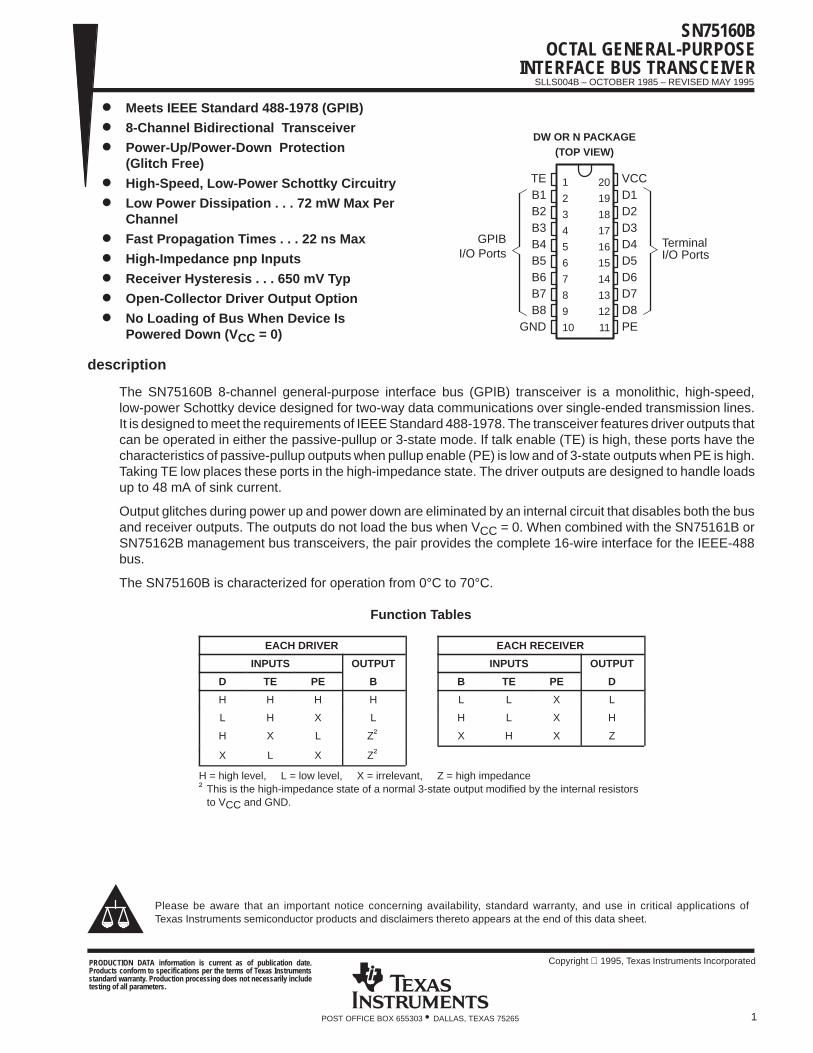
logic symbol †
D2
D3
D4
D5
D6
D7
D8
11
1
19
18
17
16
15
14
13
12
3(1 /2 )
14
EN4[RCV]
EN3[XMT]
M2[0C]
M1[3S]PE
TE
D1B12
B23
B34
B45
B56
B67
B78
B89
Designates 3-state outputsDesignates passive-pullup outputs
† This symbol is in accordance with ANSI/IEEE Std 91-1984and IEC Publication 617-12.
logic diagram (positive logic)
TerminalI/O Ports
GPIBI/O Port s
11PE
1TE
19D1
18D2
17D3
16D4
15D5
14D6
13D7
12D8
B12
B23
B34
B45
B56
B67
B78
B89
SN75160BOCTAL GENERAL-PURPOSE
INTERFACE BUS TRANSCEIVER
SLLS004B – OCTOBER 1985 – REVISED MAY 1995
3POST OFFICE BOX 655303 • DALLAS, TEXAS 75265
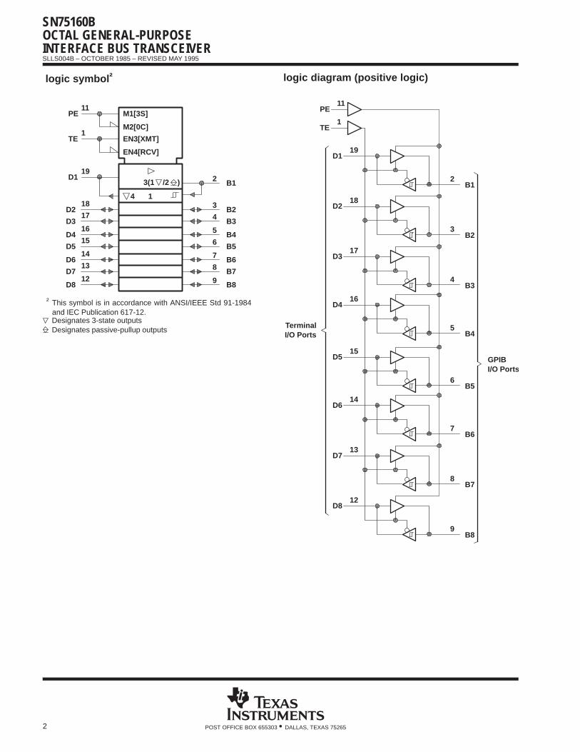
schematics of inputs and outputs
NOM9 kΩ
GND
Input
VCC
EQUIVALENT OF ALL CONTROL INPUTS EQUIVALENT OF ALL INPUT/OUTPUT PORTS
NOM4 kΩ
R(eq) 1.7 kΩNOM
10 kΩNOM
Input /Output Port
NOM4 kΩ
Driver output R (eq) = 30 Ω NOMReceiver output R (eq) = 110 Ω NOMCircuit inside dashed lines is on the driver outputs only.R(eq) = equivalent resistor
absolute maximum ratings over operating free-air temperature range (unless otherwise noted) †
Supply voltage, VCC (see Note 1) 7 V. . . . . . . . . . . . . . . . . . . . . . . . . . . . . . . . . . . . . . . . . . . . . . . . . . . . . . . . . . . . . Input voltage, VI 5.5 V. . . . . . . . . . . . . . . . . . . . . . . . . . . . . . . . . . . . . . . . . . . . . . . . . . . . . . . . . . . . . . . . . . . . . . . . . . Low-level driver output current, IOL 100 mA. . . . . . . . . . . . . . . . . . . . . . . . . . . . . . . . . . . . . . . . . . . . . . . . . . . . . . . . Continuous total power dissipation See Dissipation Rating Table. . . . . . . . . . . . . . . . . . . . . . . . . . . . . . . . . . . . . Operating free-air temperature range, TA 0°C to 70°C. . . . . . . . . . . . . . . . . . . . . . . . . . . . . . . . . . . . . . . . . . . . . . Storage temperature range, Tstg –65°C to 150°C. . . . . . . . . . . . . . . . . . . . . . . . . . . . . . . . . . . . . . . . . . . . . . . . . . . Lead temperature 1,6 mm (1/16 inch) from case for 10 seconds 260°C. . . . . . . . . . . . . . . . . . . . . . . . . . . . . . .
† Stresses beyond those listed under “absolute maximum ratings” may cause permanent damage to the device. These are stress ratings only, andfunctional operation of the device at these or any other conditions beyond those indicated under “recommended operating conditions” is notimplied. Exposure to absolute-maximum-rated conditions for extended periods may affect device reliability.
NOTES: 1. All voltage values are with respect to network ground terminal.
DISSIPATION RATING TABLE
PACKAGETA ≤ 25°C
POWER RATINGDERATING FACTORABOVE TA = 25°C
TA = 70°CPOWER RATING
DW 1125 mW 9.0 mW/°C 720 mW
N 1150 mW 9.2 mW/°C 736 mW

SN75160BOCTAL GENERAL-PURPOSEINTERFACE BUS TRANSCEIVER
SLLS004B – OCTOBER 1985 – REVISED MAY 1995
4 POST OFFICE BOX 655303 • DALLAS, TEXAS 75265
recommended operating conditions
MIN NOM MAX UNIT
Supply voltage, VCC 4.75 5 5.25 V
High-level input voltage, VIH 2 V
Low-level input voltage, VIL 0.8 V
High level output current IOHBus ports with pullups active –5.2 mA
High-level output current, IOHTerminal ports –800 µA
Low level output current IOLBus ports 48
mALow-level output current, IOLTerminal ports 16
mA
Operating free-air temperature, TA 0 70 °C
electrical characteristics over recommended ranges of supply voltage and operating free-airtemperature (unless otherwise noted)
PARAMETER TEST CONDITIONS MIN TYP† MAX UNIT
VIK Input clamp voltage II = –18 mA –0.8 –1.5 V
VhysHysteresis voltage (VIT+ – VIT–) Bus See Figure 8 0.4 0.65 V
VOH High level output voltageTerminal IOH = –800 µA, TE at 0.8 V 2.7 3.5
VVOH High-level output voltageBus IOH = –5.2 mA, PE and TE at 2 V 2.5 3.3
V
VOL Low level output voltageTerminal IOL = 16 mA, TE at 0.8 V 0.3 0.5
VVOL Low-level output voltageBus IOL = 48 mA, TE at 2 V 0.35 0.5
V
IIInput current at maximum
Terminal VI = 5 5 V 0 2 100 µAII input voltageTerminal VI = 5.5 V 0.2 100 µA
IIH High-level input current Terminal VI = 2.7 V 0.1 20 µA
IIL Low-level input current Terminal VI = 0.5 V –10 –100 µA
VI/O(b ) Voltage at bus port Driver disabledII(bus) = 0 2.5 3.0 3.7
VVI/O(bus) Voltage at bus port Driver disabledII(bus) = –12 mA –1.5
V
VI(bus) = –1.5 V to 0.4 V –1.3
VI(bus) = 0.4 V to 2.5 V 0 –3.2
Power on Driver disabled VI(b ) = 2 5 V to 3 7 V2.5
II/O(bus) Current into bus portPower on Driver disabled VI(bus) = 2.5 V to 3.7 V
–3.2 mA( )VI(bus) = 3.7 V to 5 V 0 2.5
VI(bus) = 5 V to 5.5 V 0.7 2.5
Power off VCC = 0, VI(bus) = 0 to 2.5 V –40
IOS Short circuit output currentTerminal –15 –35 –75
mAIOS Short-circuit output currentBus –25 –50 –125
mA
ICC Supply current No loadReceivers low and enabled 70 90
mAICC Supply current No loadDrivers low and enabled 85 110
mA
CI/O(b ) Bus port capacitanceVCC = 0 to 5 V, VI/O = 0 to 2 V,
16 pFCI/O(bus) Bus-port capacitance CCf = 1 MHz
I/O 16 pF
† All typical values are at VCC = 5 V, TA = 25°C.
SN75160BOCTAL GENERAL-PURPOSE
INTERFACE BUS TRANSCEIVER
SLLS004B – OCTOBER 1985 – REVISED MAY 1995
5POST OFFICE BOX 655303 • DALLAS, TEXAS 75265
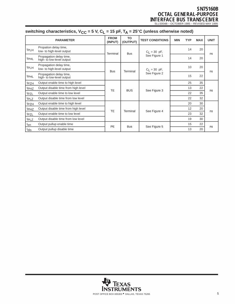
switching characteristics, V CC = 5 V, CL = 15 pF, TA = 25°C (unless otherwise noted)
PARAMETERFROM
(INPUT)TO
(OUTPUT) TEST CONDITIONS MIN TYP MAX UNIT
tPLHPropation delay time, low- to high-level output
Terminal BusCL = 30 pF,
14 20ns
tPHLPropagation delay time, high- to low-level output
Terminal Bus LSee Figure 1
14 20
ns
tPLHPropagation delay time, low- to high-level output
Bus TerminalCL = 30 pF,
10 20ns
tPHLPropagation delay time, high- to low-level output
Bus Terminal LSee Figure 2
15 22
ns
tPZH Output enable time to high level 25 35
tPHZ Output disable time from high levelTE BUS See Figure 3
13 22ns
tPZL Output enable time to low levelTE BUS See Figure 3
22 35ns
tPLZ Output disable time from low level 22 32
tPZH Output enable time to high level 20 30
tPHZ Output disable time from high levelTE Terminal See Figure 4
12 20ns
tPZL Output enable time to low levelTE Terminal See Figure 4
23 32ns
tPLZ Output disable time from low level 19 30
ten Output pullup enable timePE Bus See Figure 5
15 22ns
tdis Output pullup disable timePE Bus See Figure 5
13 20ns

SN75160BOCTAL GENERAL-PURPOSEINTERFACE BUS TRANSCEIVER
SLLS004B – OCTOBER 1985 – REVISED MAY 1995
6 POST OFFICE BOX 655303 • DALLAS, TEXAS 75265
PARAMETER MEASUREMENT INFORMATION
VOLTAGE WAVEFORMS
TEST CIRCUIT
tPHL
1.0 V
1.5 V
2.2 V
1.5 VD Input
tPLH
B Output
3 V
0 V
VOH
VOH
B
3 V
TE
CL = 30 pF(see Note B)
480 Ω
200 Ω
5 V
Output
50 Ω
D
3 VPE
Generator(see Note A)
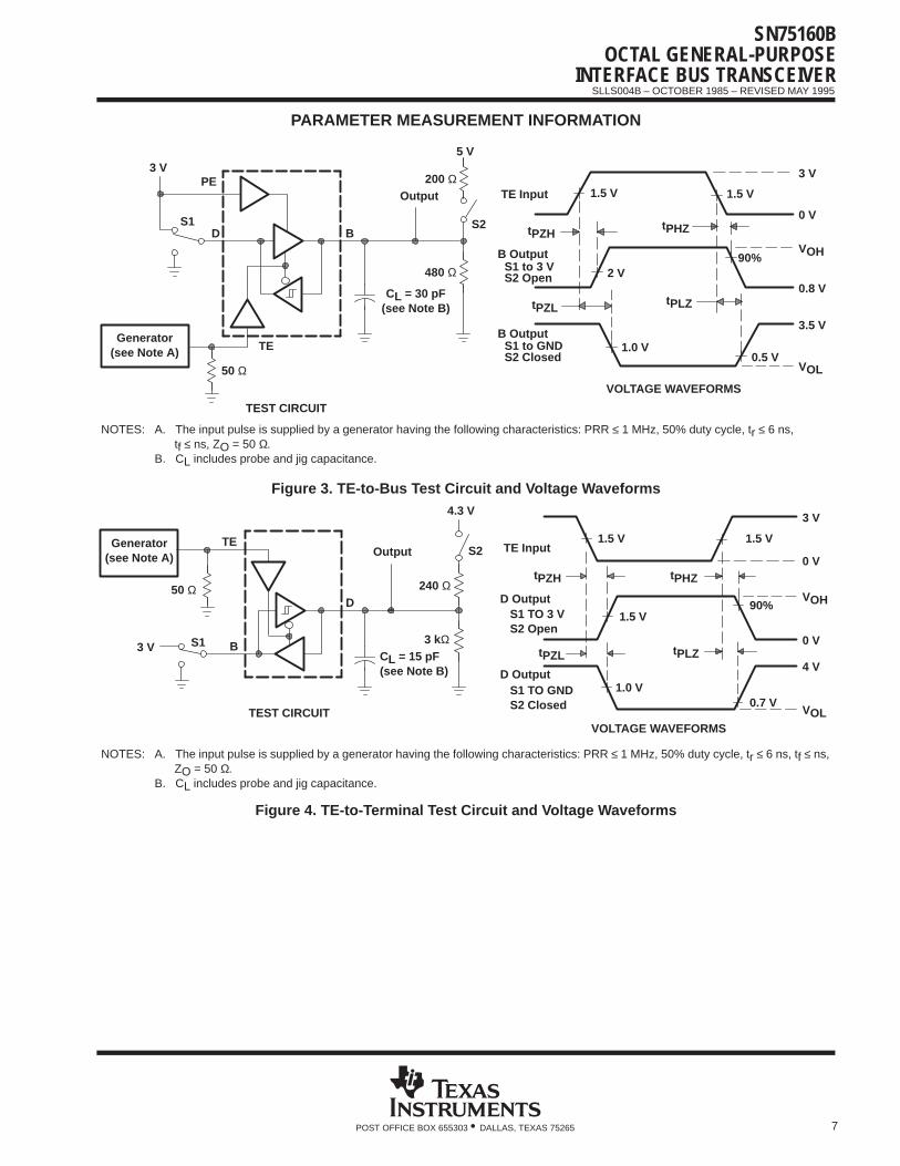
NOTES: A. The input pulse is supplied by a generator having the following characteristics: PRR ≤ 1 MHz, 50% duty cycle, tr ≤ 6 ns, tf ≤ ns, ZO = 50 Ω.
B. CL includes probe and jig capacitance.
Figure 1. Terminal-to-Bus Test Circuit and Voltage Waveforms
VOLTAGE WAVEFORMS
1.5 V
1.5 V
tPHL
1.5 V
1.5 V
tPLHDGenerator(see Note A)
CL = 30 pF(see Note B)
3 kΩ
4.3 V
Output
50 Ω
240 Ω
B Input
D Output
3 V
0 V
VOH
VOH
TEST CIRCUIT
B
TE
NOTES: A. The input pulse is supplied by a generator having the following characteristics: PRR ≤ 1 MHz, 50% duty cycle, tr ≤ 6 ns, tf ≤ ns, ZO = 50 Ω.
B. CL includes probe and jig capacitance.
Figure 2. Bus-to-Terminal Test Circuit and Voltage Waveforms
SN75160BOCTAL GENERAL-PURPOSE
INTERFACE BUS TRANSCEIVER
SLLS004B – OCTOBER 1985 – REVISED MAY 1995
7POST OFFICE BOX 655303 • DALLAS, TEXAS 75265
PARAMETER MEASUREMENT INFORMATION
VOL
3.5 V
0.8 V
VOH
0 V
3 V
tPHZ
tPLZ
0.5 V
90%
1.5 V
1.0 V
2 V
1.5 VTE Input
S2 ClosedS1 to GND
B Output
tPZL
S2 Open
tPZH
S1 to 3 VB Output
TE
S2S1B
5 V
PE
D
CL = 30 pF(see Note B)
480 Ω
200 ΩOutput
3 V
50 Ω
Generator(see Note A)
VOLTAGE WAVEFORMS
TEST CIRCUIT
NOTES: A. The input pulse is supplied by a generator having the following characteristics: PRR ≤ 1 MHz, 50% duty cycle, tr ≤ 6 ns, tf ≤ ns, ZO = 50 Ω.
B. CL includes probe and jig capacitance.
Figure 3. TE-to-Bus Test Circuit and Voltage Waveforms
0.7 V
1.5 V90%
TE Input
D Output
D Output
tPZL
1.5 V
tPZH
1.0 V
1.5 V
tPHZ
tPLZ
3 V
0 V
VOH
0 V
4 V
VOL
S2
D
S13 VCL = 15 pF(see Note B)
3 kΩ
4.3 V
Output
240 Ω
VOLTAGE WAVEFORMS
50 Ω
TEST CIRCUIT
S1 TO 3 VS2 Open
S1 TO GNDS2 Closed
B
TEGenerator(see Note A)
NOTES: A. The input pulse is supplied by a generator having the following characteristics: PRR ≤ 1 MHz, 50% duty cycle, tr ≤ 6 ns, tf ≤ ns,ZO = 50 Ω.
B. CL includes probe and jig capacitance.
Figure 4. TE-to-Terminal Test Circuit and Voltage Waveforms

SN75160BOCTAL GENERAL-PURPOSEINTERFACE BUS TRANSCEIVER
SLLS004B – OCTOBER 1985 – REVISED MAY 1995
8 POST OFFICE BOX 655303 • DALLAS, TEXAS 75265
PARAMETER MEASUREMENT INFORMATION
tdis
90%
1.5 V
2 V
ten
1.5 V
VOL = 0.8 V
VOH
0 V
3 V
RL = 480 Ω
BD
3 VTE
PEGenerator(see Note A)
CL = 15 pF(see Note B)
Output
50 Ω
PE Input
B Output
VOLTAGE WAVEFORMS
TEST CIRCUITNOTES: A. The input pulse is supplied by a generator having the following characteristics: PRR ≤ 1 MHz, 50% duty cycle, tr ≤ 6 ns, tf ≤ ns,
ZO = 50 Ω.B. CL includes probe and jig capacitance.
Figure 5. PE-to-Bus Pullup Test Circuit and Voltage Waveforms

SN75160BOCTAL GENERAL-PURPOSE
INTERFACE BUS TRANSCEIVER
SLLS004B – OCTOBER 1985 – REVISED MAY 1995
9POST OFFICE BOX 655303 • DALLAS, TEXAS 75265
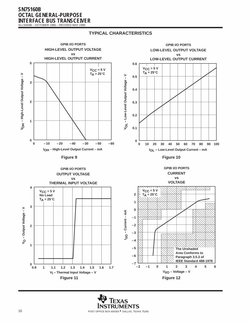
TYPICAL CHARACTERISTICS
Figure 6
VO
H –
Hig
h-Le
vel O
utpu
t Vol
tage
– V
HIGH-LEVEL OUTPUT VOLTAGEvs
HIGH-LEVEL OUTPUT CURRENT
3.5
3
2.5
2
1.5
1
0.5
–35–30–25–20–15–10–50
–40
4
0
ÎÎÎÎÎÎÎÎÎÎÎÎ
VCC = 5 VTA = 25°C
IOH – High-Level Output Current – mA
V OH
TERMINAL I/O PORTS
Figure 7IOL – Low-Level Output Current – mA
VO
L –
Low
-Lev
el O
utpu
t Vol
tage
– V
LOW-LEVEL OUTPUT VOLTAGEvs
LOW-LEVEL OUTPUT CURRENT
0.5
0.4
0.3
0.2
0.1
50403020100
60
0.6
0
VO
L
TERMINAL I/O PORTS
ÎÎÎÎÎÎÎÎÎÎÎÎ
VCC = 5 VTA = 25°C
VO
– O
utpu
t Vol
tage
– V
OUTPUT VOLTAGEvs
BUS INPUT VOLTAGE
VIT–
3.5
3
2.5
2
1.5
1
0.5
1.81.61.41.210.80.60.40.20
2
4
VI – Bus Input Voltage – V
0
VO
TERMINAL I/O PORTS
ÎÎÎÎÎÎÎÎÎÎÎÎÎÎÎÎ
VCC = 5 VNo LoadTA = 25°C
VIT+
Figure 8
SN75160BOCTAL GENERAL-PURPOSEINTERFACE BUS TRANSCEIVER
SLLS004B – OCTOBER 1985 – REVISED MAY 1995
10 POST OFFICE BOX 655303 • DALLAS, TEXAS 75265
TYPICAL CHARACTERISTICS
HIGH-LEVEL OUTPUT VOLTAGEvs
HIGH-LEVEL OUTPUT CURRENT
GPIB I/O PORTS
Figure 9
IOH – High-Level Output Current – mA
VO
H –
Hig
h-Le
vel O
utpu
t Vol
tage
– V
3
2
1
–50–30–40–20–100
–60
0
0
V OH
ÎÎÎÎÎÎÎÎÎÎÎÎ
VCC = 5 VTA = 25°C
Figure 10
IOL – Low-Level Output Current – mA
VO
L –
Low
-Lev
el O
utpu
t Vol
tage
– V
LOW-LEVEL OUTPUT VOLTAGEvs
LOW-LEVEL OUTPUT CURRENT
0.5
0.4
0.3
0.2
0.1
9080706050403020100
100
0.6
0
VO
L
GPIB I/O PORTS
ÎÎÎÎÎÎÎÎÎÎÎÎ
VCC = 5 VTA = 25°C
OUTPUT VOLTAGEvs
THERMAL INPUT VOLTAGE
Figure 11VI – Thermal Input Voltage – V
VO
– O
utpu
t Vol
tage
– V
3
2
1
1.61.51.41.31.21.110
4
0.9 1.7
VO
GPIB I/O PORTS
ÎÎÎÎÎÎÎÎÎÎÎÎÎÎÎ
VCC = 5 VNo LoadTA = 25°C
CURRENTvs
VOLTAGE
Figure 12
– C
urre
nt –
mA
2
1
0
–1
–2
–3
–4
–5
–6
543210–1–7
6
VI/O – Voltage – V
–2
ÁÁÁÁÁÁÁÁÁÁÁÁÁÁÁÁÁÁÁÁÁÁÁÁÁÁÁÁÁÁÁÁÎÎÎÎÎÎÎÎ
I I/O
GPIB I/O PORTS
ÎÎÎÎÎÎÎÎ
VCC = 5 VTA = 25°C
ÎÎÎÎÎÎÎÎÎÎÎÎÎÎÎÎÎÎÎÎÎÎÎÎÎÎÎÎÎÎÎÎÎÎÎÎÎÎÎÎÎÎÎÎÎÎÎÎÎÎÎÎÎ
The Unshaded Area Conforms to Paragraph 3.5.3 of IEEE Standard 488-1978
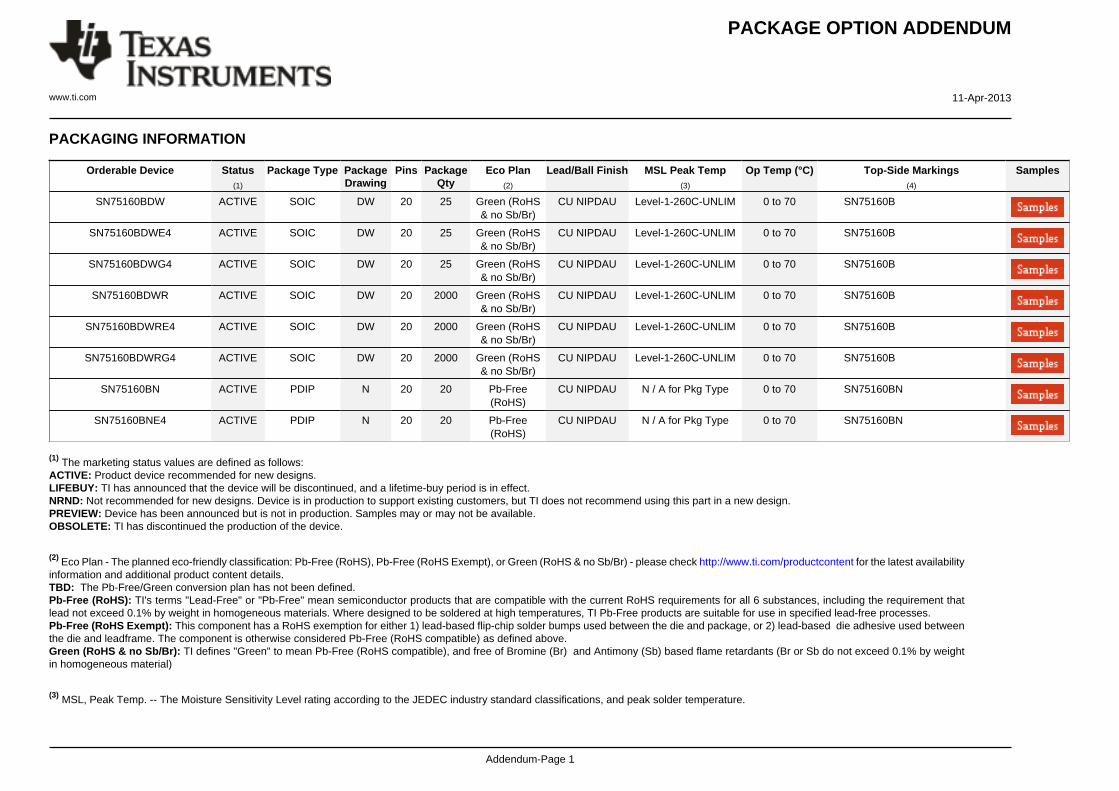
PACKAGE OPTION ADDENDUM
www.ti.com 11-Apr-2013
Addendum-Page 1
PACKAGING INFORMATION
Orderable Device Status(1)
Package Type PackageDrawing
Pins PackageQty
Eco Plan(2)
Lead/Ball Finish MSL Peak Temp(3)
Op Temp (°C) Top-Side Markings(4)
Samples
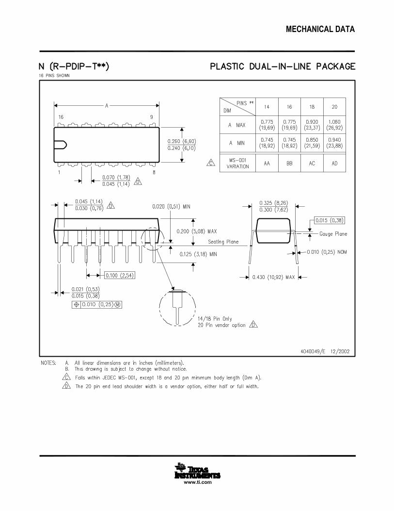
SN75160BDW ACTIVE SOIC DW 20 25 Green (RoHS& no Sb/Br)
CU NIPDAU Level-1-260C-UNLIM 0 to 70 SN75160B
SN75160BDWE4 ACTIVE SOIC DW 20 25 Green (RoHS& no Sb/Br)
CU NIPDAU Level-1-260C-UNLIM 0 to 70 SN75160B
SN75160BDWG4 ACTIVE SOIC DW 20 25 Green (RoHS& no Sb/Br)
CU NIPDAU Level-1-260C-UNLIM 0 to 70 SN75160B
SN75160BDWR ACTIVE SOIC DW 20 2000 Green (RoHS& no Sb/Br)
CU NIPDAU Level-1-260C-UNLIM 0 to 70 SN75160B
SN75160BDWRE4 ACTIVE SOIC DW 20 2000 Green (RoHS& no Sb/Br)
CU NIPDAU Level-1-260C-UNLIM 0 to 70 SN75160B
SN75160BDWRG4 ACTIVE SOIC DW 20 2000 Green (RoHS& no Sb/Br)
CU NIPDAU Level-1-260C-UNLIM 0 to 70 SN75160B
SN75160BN ACTIVE PDIP N 20 20 Pb-Free(RoHS)
CU NIPDAU N / A for Pkg Type 0 to 70 SN75160BN
SN75160BNE4 ACTIVE PDIP N 20 20 Pb-Free(RoHS)
CU NIPDAU N / A for Pkg Type 0 to 70 SN75160BN
(1) The marketing status values are defined as follows:ACTIVE: Product device recommended for new designs.LIFEBUY: TI has announced that the device will be discontinued, and a lifetime-buy period is in effect.NRND: Not recommended for new designs. Device is in production to support existing customers, but TI does not recommend using this part in a new design.PREVIEW: Device has been announced but is not in production. Samples may or may not be available.OBSOLETE: TI has discontinued the production of the device.
(2) Eco Plan - The planned eco-friendly classification: Pb-Free (RoHS), Pb-Free (RoHS Exempt), or Green (RoHS & no Sb/Br) - please check http://www.ti.com/productcontent for the latest availabilityinformation and additional product content details.TBD: The Pb-Free/Green conversion plan has not been defined.Pb-Free (RoHS): TI's terms "Lead-Free" or "Pb-Free" mean semiconductor products that are compatible with the current RoHS requirements for all 6 substances, including the requirement thatlead not exceed 0.1% by weight in homogeneous materials. Where designed to be soldered at high temperatures, TI Pb-Free products are suitable for use in specified lead-free processes.Pb-Free (RoHS Exempt): This component has a RoHS exemption for either 1) lead-based flip-chip solder bumps used between the die and package, or 2) lead-based die adhesive used betweenthe die and leadframe. The component is otherwise considered Pb-Free (RoHS compatible) as defined above.Green (RoHS & no Sb/Br): TI defines "Green" to mean Pb-Free (RoHS compatible), and free of Bromine (Br) and Antimony (Sb) based flame retardants (Br or Sb do not exceed 0.1% by weightin homogeneous material)
(3) MSL, Peak Temp. -- The Moisture Sensitivity Level rating according to the JEDEC industry standard classifications, and peak solder temperature.
PACKAGE OPTION ADDENDUM
www.ti.com 11-Apr-2013
Addendum-Page 2
(4) Multiple Top-Side Markings will be inside parentheses. Only one Top-Side Marking contained in parentheses and separated by a "~" will appear on a device. If a line is indented then it is acontinuation of the previous line and the two combined represent the entire Top-Side Marking for that device.
Important Information and Disclaimer:The information provided on this page represents TI's knowledge and belief as of the date that it is provided. TI bases its knowledge and belief on informationprovided by third parties, and makes no representation or warranty as to the accuracy of such information. Efforts are underway to better integrate information from third parties. TI has taken andcontinues to take reasonable steps to provide representative and accurate information but may not have conducted destructive testing or chemical analysis on incoming materials and chemicals.TI and TI suppliers consider certain information to be proprietary, and thus CAS numbers and other limited information may not be available for release.
In no event shall TI's liability arising out of such information exceed the total purchase price of the TI part(s) at issue in this document sold by TI to Customer on an annual basis.

TAPE AND REEL INFORMATION
*All dimensions are nominal
Device PackageType
PackageDrawing
Pins SPQ ReelDiameter
(mm)
ReelWidth
W1 (mm)
A0(mm)
B0(mm)
K0(mm)
P1(mm)
W(mm)
Pin1Quadrant
SN75160BDWR SOIC DW 20 2000 330.0 24.4 10.8 13.0 2.7 12.0 24.0 Q1
SN75160BDWR SOIC DW 20 2000 330.0 24.4 10.8 13.3 2.7 12.0 24.0 Q1
PACKAGE MATERIALS INFORMATION
www.ti.com 3-Jan-2013
Pack Materials-Page 1

*All dimensions are nominal
Device Package Type Package Drawing Pins SPQ Length (mm) Width (mm) Height (mm)
SN75160BDWR SOIC DW 20 2000 367.0 367.0 45.0
SN75160BDWR SOIC DW 20 2000 367.0 367.0 45.0
PACKAGE MATERIALS INFORMATION
www.ti.com 3-Jan-2013
Pack Materials-Page 2
www.ti.com
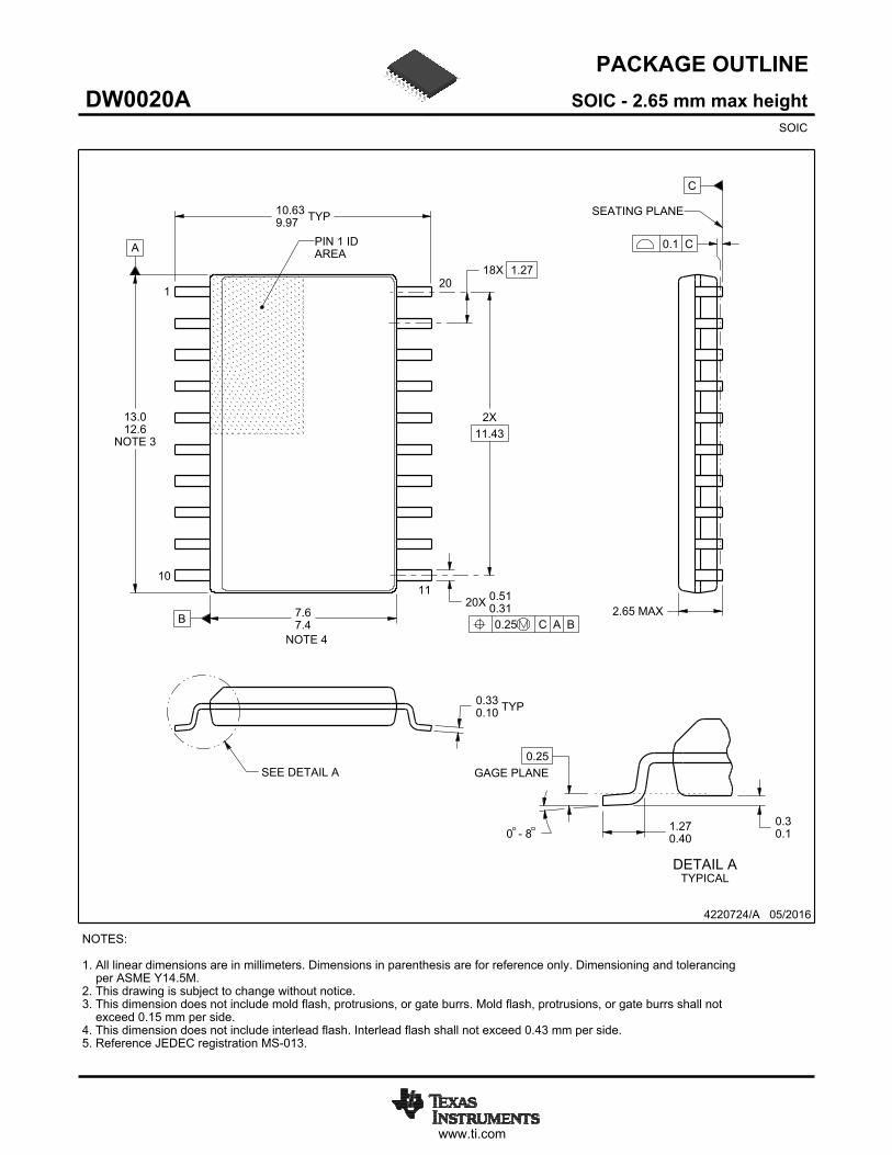
PACKAGE OUTLINE
C
TYP10.639.97
2.65 MAX
18X 1.27
20X 0.510.31
2X11.43
TYP0.330.10
0 - 80.30.1
0.25GAGE PLANE
1.270.40
A
NOTE 3
13.012.6
B 7.67.4
4220724/A 05/2016
SOIC - 2.65 mm max heightDW0020ASOIC
NOTES: 1. All linear dimensions are in millimeters. Dimensions in parenthesis are for reference only. Dimensioning and tolerancing per ASME Y14.5M. 2. This drawing is subject to change without notice. 3. This dimension does not include mold flash, protrusions, or gate burrs. Mold flash, protrusions, or gate burrs shall not exceed 0.15 mm per side. 4. This dimension does not include interlead flash. Interlead flash shall not exceed 0.43 mm per side.5. Reference JEDEC registration MS-013.
120
0.25 C A B
1110
PIN 1 IDAREA
NOTE 4
SEATING PLANE
0.1 C
SEE DETAIL A
DETAIL ATYPICAL
SCALE 1.200
www.ti.com
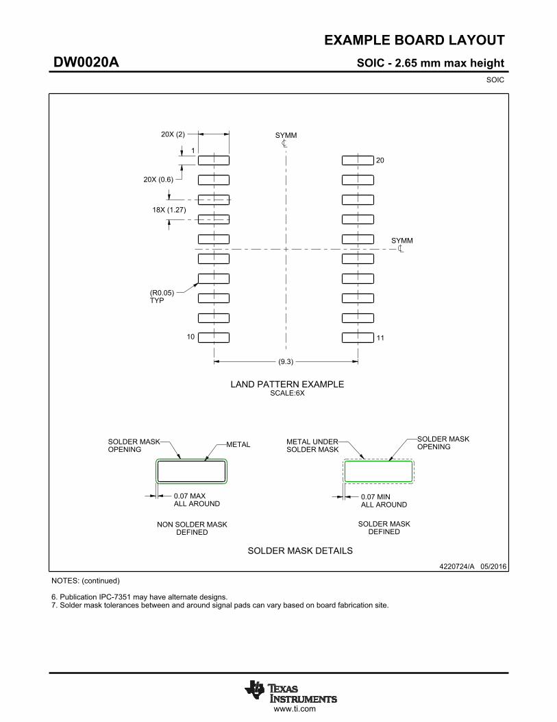
EXAMPLE BOARD LAYOUT
(9.3)
0.07 MAXALL AROUND
0.07 MINALL AROUND
20X (2)
20X (0.6)
18X (1.27)
(R )TYP
0.05
4220724/A 05/2016
SOIC - 2.65 mm max heightDW0020ASOIC
SYMM
SYMM
LAND PATTERN EXAMPLESCALE:6X
1
10 11
20
NOTES: (continued) 6. Publication IPC-7351 may have alternate designs. 7. Solder mask tolerances between and around signal pads can vary based on board fabrication site.
METALSOLDER MASKOPENING
NON SOLDER MASKDEFINED
SOLDER MASK DETAILS
SOLDER MASKOPENING
METAL UNDERSOLDER MASK
SOLDER MASKDEFINED
www.ti.com
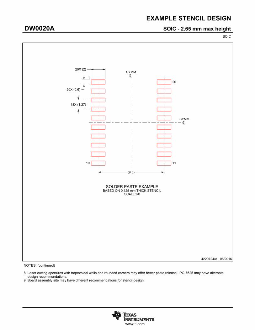
EXAMPLE STENCIL DESIGN
(9.3)
18X (1.27)
20X (0.6)
20X (2)
4220724/A 05/2016
SOIC - 2.65 mm max heightDW0020ASOIC
NOTES: (continued) 8. Laser cutting apertures with trapezoidal walls and rounded corners may offer better paste release. IPC-7525 may have alternate design recommendations. 9. Board assembly site may have different recommendations for stencil design.
SYMM
SYMM
1
10 11
20
SOLDER PASTE EXAMPLEBASED ON 0.125 mm THICK STENCIL
SCALE:6X

IMPORTANT NOTICE
Texas Instruments Incorporated and its subsidiaries (TI) reserve the right to make corrections, enhancements, improvements and otherchanges to its semiconductor products and services per JESD46, latest issue, and to discontinue any product or service per JESD48, latestissue. Buyers should obtain the latest relevant information before placing orders and should verify that such information is current andcomplete. All semiconductor products (also referred to herein as “components”) are sold subject to TI’s terms and conditions of salesupplied at the time of order acknowledgment.TI warrants performance of its components to the specifications applicable at the time of sale, in accordance with the warranty in TI’s termsand conditions of sale of semiconductor products. Testing and other quality control techniques are used to the extent TI deems necessaryto support this warranty. Except where mandated by applicable law, testing of all parameters of each component is not necessarilyperformed.TI assumes no liability for applications assistance or the design of Buyers’ products. Buyers are responsible for their products andapplications using TI components. To minimize the risks associated with Buyers’ products and applications, Buyers should provideadequate design and operating safeguards.TI does not warrant or represent that any license, either express or implied, is granted under any patent right, copyright, mask work right, orother intellectual property right relating to any combination, machine, or process in which TI components or services are used. Informationpublished by TI regarding third-party products or services does not constitute a license to use such products or services or a warranty orendorsement thereof. Use of such information may require a license from a third party under the patents or other intellectual property of thethird party, or a license from TI under the patents or other intellectual property of TI.Reproduction of significant portions of TI information in TI data books or data sheets is permissible only if reproduction is without alterationand is accompanied by all associated warranties, conditions, limitations, and notices. TI is not responsible or liable for such altereddocumentation. Information of third parties may be subject to additional restrictions.Resale of TI components or services with statements different from or beyond the parameters stated by TI for that component or servicevoids all express and any implied warranties for the associated TI component or service and is an unfair and deceptive business practice.TI is not responsible or liable for any such statements.Buyer acknowledges and agrees that it is solely responsible for compliance with all legal, regulatory and safety-related requirementsconcerning its products, and any use of TI components in its applications, notwithstanding any applications-related information or supportthat may be provided by TI. Buyer represents and agrees that it has all the necessary expertise to create and implement safeguards whichanticipate dangerous consequences of failures, monitor failures and their consequences, lessen the likelihood of failures that might causeharm and take appropriate remedial actions. Buyer will fully indemnify TI and its representatives against any damages arising out of the useof any TI components in safety-critical applications.In some cases, TI components may be promoted specifically to facilitate safety-related applications. With such components, TI’s goal is tohelp enable customers to design and create their own end-product solutions that meet applicable functional safety standards andrequirements. Nonetheless, such components are subject to these terms.No TI components are authorized for use in FDA Class III (or similar life-critical medical equipment) unless authorized officers of the partieshave executed a special agreement specifically governing such use.Only those TI components which TI has specifically designated as military grade or “enhanced plastic” are designed and intended for use inmilitary/aerospace applications or environments. Buyer acknowledges and agrees that any military or aerospace use of TI componentswhich have not been so designated is solely at the Buyer's risk, and that Buyer is solely responsible for compliance with all legal andregulatory requirements in connection with such use.TI has specifically designated certain components as meeting ISO/TS16949 requirements, mainly for automotive use. In any case of use ofnon-designated products, TI will not be responsible for any failure to meet ISO/TS16949.
Products ApplicationsAudio www.ti.com/audio Automotive and Transportation www.ti.com/automotiveAmplifiers amplifier.ti.com Communications and Telecom www.ti.com/communicationsData Converters dataconverter.ti.com Computers and Peripherals www.ti.com/computersDLP® Products www.dlp.com Consumer Electronics www.ti.com/consumer-appsDSP dsp.ti.com Energy and Lighting www.ti.com/energyClocks and Timers www.ti.com/clocks Industrial www.ti.com/industrialInterface interface.ti.com Medical www.ti.com/medicalLogic logic.ti.com Security www.ti.com/securityPower Mgmt power.ti.com Space, Avionics and Defense www.ti.com/space-avionics-defenseMicrocontrollers microcontroller.ti.com Video and Imaging www.ti.com/videoRFID www.ti-rfid.comOMAP Applications Processors www.ti.com/omap TI E2E Community e2e.ti.comWireless Connectivity www.ti.com/wirelessconnectivity
Mailing Address: Texas Instruments, Post Office Box 655303, Dallas, Texas 75265Copyright © 2016, Texas Instruments Incorporated
Related Documents