DEMAND RESPONSE MANAGEMENT USING SMART METERS By: Srividhya.B ,Summer Intern Fellow, Guide / Supervisor : Dr. K.S. Swarup College: S.S.N College Of Engineering, email:[email protected] Duration : From 18.05.2015 to 17.07.2015 Dept of Electrical Engineering. Indian Institute of Technology, Madras Abstract: A demand response based dynamic load control scheme is employed in the proposed model where ,electric power assignment is not only based on initial data of the household in the local grid, but it also takes some real-time information into consideration. A technique called Multi Agent System is employed in which electric Smart Meters and distributed controllers are used to communicate between various households in the local grid and between various houses within a particular household thus establishing an economical Power Market. An effective cost based power sharing scenario in a proposed architectural network was developed and implemented using JADE and MATLAB. Objectives: To develop an architecture for Demand response management system of a household network. To propose and implement an effective power scheduling communication protocol using smart meters. To make use of the Smart meters in establishing an effective power market network. Results(MATLAB) Schematic Results (JADE) Conclusions: Consumer can schedule operation of regulatable loads based on their priorities. Establishment of effective power Market strategies. Making efficient use of unused power. Exploiting the functions of the Smart Meters to the fullest to achieve an effective power market protocol in the local neighbourhood. .

Welcome message from author
This document is posted to help you gain knowledge. Please leave a comment to let me know what you think about it! Share it to your friends and learn new things together.
Transcript

DEMAND RESPONSE MANAGEMENT USING SMART METERS
By: Srividhya.B ,Summer Intern Fellow, Guide / Supervisor : Dr. K.S. Swarup
College: S.S.N College Of Engineering, email:[email protected]
Duration : From 18.05.2015 to 17.07.2015
Dept of Electrical Engineering. Indian Institute of Technology, Madras
Abstract: A demand response based dynamic load control scheme is employed in the proposed model where ,electric power assignment is not only
based on initial data of the household in the local grid, but it also takes some real-time information into consideration. A technique called Multi
Agent System is employed in which electric Smart Meters and distributed controllers are used to communicate between various households in the
local grid and between various houses within a particular household thus establishing an economical Power Market. An effective cost based power
sharing scenario in a proposed architectural network was developed and implemented using JADE and MATLAB.
Objectives: To develop an architecture for Demand response
management system of a household network.
To propose and implement an effective power scheduling
communication protocol using smart meters.
To make use of the Smart meters in establishing an effective
power market network.
Results(MATLAB)
Schematic Results (JADE)
Conclusions:
Consumer can schedule operation of
regulatable loads based on their
priorities.
Establishment of effective power
Market strategies.
Making efficient use of unused power.
Exploiting the functions of the Smart
Meters to the fullest to achieve an
effective power market protocol in the
local neighbourhood.
.

HOME AUTOMATION USING POWERLINE COMMUNICATION
Summer Intern Fellowship: EE15SFP2169, Guide / Supervisor Dr Devandra Jalihal
College / Institution: IIITDM Kancheepuram, email:[email protected] , Duration 20-05-15 to 17-07-15
Dept of Electrical Engineering. Indian Institute of Technology, Madras
Abstract: From large-scale machines to micron size chips have one thing in common they are driven by A.C mains but, in general, data
is never sent or received through them. The project aims at using power line communication between devices to communicate the
load status/information . Having the details of all devices in an apartment at a central hub enables intelligently use this data for power
conservation. A request based protocol with acknowledgement was implemented on the PIC microcontrollers to communicate the
information to a central node(Master).
Objectives:
To implement the communication protocol on the PIC micro controllers
to transmit the acquired data.
Implement a repeater that enables long distance
communication
Packet Format
.
Data Communication
Experimental Setup
Results
Conclusion : A central hub within an apartment can acquire data regarding power consumption of all the houses, and intelligently
use this data for power conservation, all without using any extra wiring exclusively for communication

DYNAMIC USER ASSOCIATION IN NETWORK SIMULATOR 3
Name : S.Varsha, Summer Fellowship Intern, Guide : Dr. Venkatesh Ramaiyan
Institution : SSN College of Engineering, email: [email protected],
Duration: From 22-5-2015 to 17-7-2015
Dept of Electrical Engineering. Indian Institute of Technology, Madras
Abstract: Network Simulator-3 is an open-source discrete event network simulator publicly available for research, development and use, under the
GNU GPLv2 license. The available model set in ns-3 focuses on modelling how Internet protocols and networks work. New models are built and
existing models are debugged from the contributions made by the research community. Dynamic user association in WLANs requires the wireless
clients to assess and identify the “best” APs to affiliate with based on certain metrics such as load and SNR.
Objectives:
To study and understand the features of the existing Wi-Fi
module in ns-3 and trace the flow of function calls during
different phases of user association.
Implement and understand the association of a client with
AP and also the data transfer when the client is mobile.
Implement a Dynamic user association algorithm in ns-3.
Wifi Architecture and Flow of function calls
Pcap Trace – Wireshark
(Mobile Client problem)
Future Work: Implementation of a
dynamic user association algorithm in
ns-3 could be done. Unlike the present
scenario in ns-3, where a client
automatically gets associated to an AP
immediately after hearing a beacon from
the AP, Dynamic User Association helps
to enable wireless clients choose “best”
APs based on different metrics.
.
(AP side) (client side)
Wi-Fi architecture in ns-3 Flow of Beacon from
AP to client
Animation Trace – Netanim
Reference :
https://www.nsnam.org/docs/tutorial/htm
l/

RESEARCH POSTER PRESENTATION DESIGN © 2012
www.PosterPresentations.com
Introduction
Consider an example where the muscles
below the elbow are paralyzed while the
biceps & triceps have almost full movement.
The bicep muscle can be used to trigger the
electrical muscle stimulator in order to
contract the paralyzed muscle.
This can be further modified by triggering
the stimulator only when a sequence of
action is done ( i.e to twitch the predefined
muscle in a sequence to trigger the electrical
muscle stimulator. ) Hence, it can restore
the movement of paralyzed muscle with
some degrees of freedom.
Electromyography
EMG is a technique for evaluating and
recording the electrical activity produced
by skeletal muscles. These signals are
essentially made up of superimposed motor
unit action potentials (MUAPs) from
several motor units. For a thorough
analysis, the measured EMG signals can be
decomposed into their constituent MUAPs.
For the trigger, we need only the magnitude
of the EMG signal and we don’t really have
to decompose the signal.
Functional Electrical Stimulator
Functional Electrical Stimulator, also
known as neuromuscular electrical
stimulation (NMES)
or electromyostimulation, is the elicitation
of muscle contraction using electric
impulses. The impulses are generated by a
device and delivered through electrodes on
the skin in direct proximity to the muscles
to be stimulated. The impulses mimic the
action potential coming from the central
nervous system, causing the muscles to
contract.
The circuit has six
stages… First stage is a difference amplifier INA106 with gain G=110. It amplifies the difference in voltage between the inverting and non-inverting terminals. Mid- muscle electrode is connected to the inverting terminal and the end muscle electrode is connected to non-inverting terminal.
Stage 2is a simple inverting amplifier with gain equal to 15. Output from the difference amplifier is in the order of 0.1 volts and hence it must be amplifier before rectification. Stage 3 is a first order high pass filter with cutoff frequency of 10Hz used to block the DC offset and low frequency noise. It is usually designed for cutoff frequency 10~20Hz.
Stage 4: The mean of the raw EMG signal is zero. Once this signal is passed through a full wave rectifier, it has both DC and AC components. AC component is removed using a low pass filter in the next stage. Hence, the magnitude of DC voltage is proportional to strain on the muscle.
Stage 5: The output of the rectifier is a pulsating DC signal. Using a low pass filter (with cutoff frequency between 2~4Hz) we can pass on the smooth-DC signal to the next stage.
Stage 6:Stage 6 is an inverting amplifier with variable gain (G= 0~10). This stage is used for two reasons. Firstly, to cancel out the signal invert due to stage 5 (low pass filter) as the controller can read only positive voltage levels. Secondly, the gain can be varied which helps in calibration and fine tuning. The output is sampled at using a controller and the FES is triggered accordingly.
EMG circuit working
Circuit
Result
Using Electromyography Signals and IMU to Trigger Muscle Stimulator for Stroke Induced Movement Disorder
Principal Investigator:Dr. Ramakrishna Pasumathy
Student Researcher: Raghavendra P
Working overview
Amplifier and Filter design for EMG
The setup consists of two parts i.e. The
EMG which monitors the muscle activity of
our interest and accordingly, triggers the
muscle stimulator which in turn contracts
the paralyzed muscle by firing a sequence
of electrical currents to
activate nerves innervating extremities
affected by paralysis. Figure show the magnitude and frequency spectrum of the EMG signal taken over 25 seconds at 2 kHz. There is a There is increase in the amplitude of the signal when the muscle is flexed. From the frequency spectrum, most of the significant component is spread between 10Hz and 100Hz.
Conclusio
n We have used the EMG thresholds to
trigger the FES, therefore restoring the
movement of paralytic muscle using a
functional muscle. Further, we would
want to use an array of electrodes for
stimulation and also implement an
adaptive calibration technique with a
feedback control from the sensor fusion.

INTERFACING THE BROWSER AND SERVER USING GOLANG
Summer Intern Fellowship, Guide: Dr.Giridhar.K, Dr.Sendil Ramkumar, Dr.Arun Ayyar
College / Institution: SSN College of Engineering, email: [email protected] DurationMay-July
Dept of Electrical Engineering. Indian Institute of Technology, Madras
Abstract: Simulation for Electrical Engineers is always tedious and takes lot of efforts to write in languages
like C/C++. So,, Golang is recently developed language which overcomes many obstacles such as interfacing
and processor speeds and time
Objectives:
To develop an interface which enables easy access to
computing path loss for different path loss models
Compare the results between different pathloss models for
the same environment
Front End Display
Sample Results Conclusion
References
www.copterlabs.com/blog/json-what-it-is-how-it-works-how-to-use-it/
https://www.nsnam.org/docs/models/html/propagation.html
.
Thus this interfacing will
enable easy access to SINR
calculation for various
parameter of the antenna.
It helps in making the research
user friendly and saves coding
time for future researchers

Pedestrian Detection and Advanced Driver Assistance Systems By N.Srinath, Summer Fellowship Intern - 2015, Guided by Dr.A.N.Rajagopalan
Institution: SSN College of Engineering, email: [email protected]
Duration : From 21-5-15 to 17-5-15
Dept of Electrical Engineering. Indian Institute of Technology, Madras
Abstract : Pedestrian detection is an ADAS system with established datasets and robust algorithms helping in preventing automobile
accidents using Stereo Vision. HoG*+SVM is an established algorithm which provides better results in trainable systems.
Benchmarks and types of detection are discussed. Hough transform is used to identify the different lanes in lane detection, and spline
fitting is used for extrapolation. Speed braker detection uses auto-thresholding and color mapping for detection. Deep learning and
Hough Forest extensions are discussed. ( HoG – Histogram of Oriented Gradients .)
Objectives :
Study and analyse the paradigms in Advanced Driver Assistance
Systems and in particular Pedestrian Detection systems in real time
environments for pedestrian safety especially in non-ideal, Indian
road conditions.
Implement Pedestrian Detection , lane detection and speed-
braker detection.
HoG flowchart + SVM and Hough Lines
Result graph and Outputs.
Conclusions:
HoG,SVM gives a detection
rate of 14%, with a false +ve
of 84%.
Lane detection, speed braker
detection are achieved using
Hough transform and triangular
thresholding.
References : 1.Dalal, N., Triggs, HoG, CVPR.
2. Video Lane estimation,
McCall, 2005

DATA COMPRESSION OF INDIAN LANGUAGES
Summer Intern Fellowship, Guide / Supervisor DR. Devendra Jalihal
College / Institution: SASTRA UNIVERSITY , email: [email protected] Duration From 22/5- to 27/6
Dept of Electrical Engineering. Indian Institute of Technology, Madras
Abstract: In GSM environments, an SMS can contain up to 140 bytes(standard 8 bit bytes) of message data.. If we need to send a SMS containing
characters that are not a part of the standard GSM 7-bit set (Hindi, Tamil),then the text needs to be encoded in Unicode UCS-2 format where each
message size is limited to 70 16-bit characters. We have developed a mechanism such that the text to be encoded is split up in the form of clusters,
and the most occurring character occupies least amount of bit space and least occurring occupies most number of bits. Using this cluster
mechanism we can reduce the bit space occupied by a character.
Objectives:
To develop a Huffman algorithm to encode and decode the
data.
To improve the data compression rate to less than 7-bit.
To create a probability and frequency table of the encoded
characters.
Results
Results Results
*Data Compression of Indian languages
Conclusions:
With Huffman coding as the basis we
were able to encode and decode the data
successfully.
Also a probability and frequency table
of characters were created
. DataSource:http://www.geeksforg
eeks.org/greedy-algorithms-set-3-
huffman-coding/

BIOLOGICAL 3-D SEGMENTATION
Summer Intern Fellowship, Guide / Supervisor: Dr. Kaushik Mitra
College / Institution: Jadavpur Uniersity, email: [email protected] Duration From 22.5.15 to 24.7.15
Dept of Electrical Engineering. Indian Institute of Technology, Madras
Abstract: Biomedical image processing is a very broad field; it covers biomedical signal gathering, image forming, picture processing, and image
display to medical diagnosis based on features extracted from images. Processing and analysing these images in 2D do not convey total information
and therefore 3D reconstruction of images are required to get all the desired information like volume and surface area of objects of interest. My
project is about the 3D reconstruction and segmentation of infected liver cells, ultimate objective being able to compare the parameters of healthy
cells and infected cells in a liver of a human being.
Objectives:
To segment liver tissue Z stack in 3D which
consists of nuclei, cells and bi-canal tubes.
Input Data: 3D Z Stack of Liver Tissue
Approach: i) Direct 3-D Segmentation (With the help of software like FIJI, FarSight)
ii) 2-D to 3-D Segmentation (Our method)
Segment each image in 2D by Otsu thresholding and link them across Z-stack to form a 3D
reconstructed image by tracking centroid and area overlap of each object.
3D Segmentation of Cell
Data Source:
National Centre For Biological Science,
Bangalore.
Results: 3D Segmentation of Nuclei
2D segmented image
Corrected 3D Segments
Post-Processing Manual Intervention
2D segmented image
Corrected 3D Segments
Nuclei
Cells
Bicanal
Tubes

DSC APPLICATIONS IN POWER ELECTRONICS & DRIVES
Summer Intern Fellowship, Guide / Supervisor Dr. Lakshmi Narasamma
College / Institution: SJCE, Mysore, email: [email protected] Duration: 22-5-2015 to 17-7-2015
Dept of Electrical Engineering. Indian Institute of Technology, Madras
Abstract: Digital Signal Controllers are widely used for different applications. Control of electric drive systems with Digital Signal Processors (DSP) is today a very common task. For applications which demands extensive calculation power and speed, they make the suitable candidates. In Power Electronics, to obtain a very quick, robust control performance, DSC's are used. The C2000 series of processor have been widely used for motor drives' applications where the control algorithm is coded into the DSP.
Objectives:
To Study, Analyze and Test the Digital Signal Controller
TMS320F28335 development board.
Applications : Software & CPU Timer, PWM, DAC, ADC,SCI
To build 3 Phase AC-DC-AC Converter.
To use PWM technique for Inverter using TMS320F28335
V/f Control of Induction Motor
3Phase AC-DC-AC Converter
Inverter Testing Results
Conclusions:
Various Applications of DSC like
Software & CPU Timer, DAC,ADC,SCI
were tested and most accurate results
were obtained.
The developed board fire PWM pulses
to the gates of the inverter switches. The
motor was fed by the 3-phase inverter.
Control technique was coded in the DSC
with appropriate sensors of position of
the rotor shaft from the shaft encoders.
.
TMS320F28335 Board
DAC & ADC Result

Control of Mobile Inverted Pendulum
Summer Intern Fellowship, Name: Sneha P, Guide: Dr. Arun D. Mahindrakar
Institution: M. S. Ramaiah Institute of Technology, email: [email protected]
Dept of Electrical Engineering. Indian Institute of Technology, Madras
Abstract: Mobile robots have widespread applications in remote monitoring, surveillance, disaster zone search and space exploration. Inverted
pendulum is a two wheel unstable robotic platform that balances itself up in the vertical position with reference to the ground. The resulting
implementation manages to stabilize the robot in an upright position and reject disturbances such as pushes. The position and reduced attitude
control laws can be used for stabilizing the robots to an arbitrary location in the horizontal plane.
Objectives:
•Understanding the schematic and modeling of MIP along with
the control laws and its implications.
•Learning the hardware and position stabilization of MIP
•Triangle and square formations using MIPs and waypoint
trajectory tracking.
Model of MIP
Formation Results
Future work: A smooth control law
can be designed for the MIP robot to
have an almost global domain-of-
attraction for the one-dimensional
equilibrium submanifold. Obstacle
avoidance and formation control of
MIP robots can be evaluated using
the existing control law as the inner-
loop.
Reference: http://docslide.us/documents/stabilization-of-a-mobile-inverted-pendulum.html

DESIGN OF POWER AMPLIFIERS
Summer Fellowship Programme-2015, Guide / Supervisor:Dr.S.Aniruddhan
College / Institution: Amrita School of Engineering, email: [email protected]
Duration From 27.05.2015 to 17.07.2015
Dept of Electrical Engineering. Indian Institute of Technology, Madras
OBJECTIVE: To design a PA for the LTE cellular system is designed and simulated in UMC130nm CMOS process. The PA is configured to operate in 1.8GHz frequency band. It is capable of delivering modulated output power of 5dBm to a 50 load while meeting the stringent linearity requirements of the LTE standard. The PA was designed for a 1dB compression point of 12.1dBm and a phase distortion of 3degrees which is capable of giving desirable ACPR values.
DESIGN FLOW:
•The first step was to do a paper design and then proceed with the schematic in the software.
•For a 1db compression point of 12.1dBm it is calculated to have a value of 45mA of bias current.
•The first step in the circuit design is to set gm3 of the amplifier transistor should be set to zero by plotting gm3 curves (keeping Vds a constant)with respect to the VGS and then fix the value of Vgs to the point where it is intersecting x-axis.
•The next step was to fix VDD based on the output power required which turned out to be 2V for this design for an output power of 5dbm
•A Cascode transistor is added in order to increase the isolation between the input and output ports.
•Large on chip inductances are impractical and they have large DC resistances that causes undesired voltage drops. So, a resonant tank is added at the drain of the cascode for using an RF inductor and a capacitor.
•Based on the Voltage gain required gm of both the transistors is fixed and matched accordingly by setting W and multiplier of both the transistors .Length is maintained to be minimum.
RESULTS: PLOTS
CONCLUSION: Plots shown
in the figure gives the 1dB
compression point, phase distortion
and power gain.
Power Amplifier with required
specifications was designed and
verified. The design can be extended
to a dual band by sharing a common
inductor between both the circuits..

PROGRAMMING OF ROBOTS USING MATLAB SIMULINK
Summer Intern Fellowship, Guide / Supervisor Dr. Bharath Bhikkaji
College / Institution: R.V. College of Engineering, email: [email protected]
Duration From _22nd May – to- 8th July
Dept of Electrical Engineering. Indian Institute of Technology, Madras
Abstract: The present work uses MATLAB Simulink tools and LEGO Mindstorms EV3 Education kit to program robots to effectively realize an
Obstacle Sensing bot ,a Line Follower bot and a Self Balancing bot.
Obstacle Sensing Robot
Developed Program
.
Line Follower Robot
Developed Program
1ST THRESHOLD : If distance from Obstacle < 25 cm
TRUE : Decrease Speed by halving Gain
FALSE : Continue
2ND THRESHOLD : If distance from Obstacle < 15 cm
TRUE : Speed = 0
FALSE : Continue
The robot uses feedback from the Color sensor to track the
line. The feedback from the motor encoders is used to
maintain forward velocity. Two Proportional-Integral-
Derivative(PID) controllers are used to control the velocity
and tracking.
Self Balancing Robot
Developed Program
While both signals (Speed and Turn angle)
are 0, the robot remains balanced in one
place. A positive value for speed causes the
robot to move forward and a negative value
to go in the reverse direction. A positive value
for turn angle causes the robot to turn right
and a negative value to turn left.

SPO2 MEASUREMENT, MICROCONTROLLER AND BLUETOOTNH MODULE INTRIGATION
SAIRAM MADAMALA,Summer Intern Fellowship, Guide / Supervisor Dr. V. Jagadeesh Kumar
Institution: SRM UNIVERSITY, email: [email protected] From: 17-05 to 17-07-2105
Dept of Electrical Engineering. Indian Institute of Technology, Madras
Abstract: Vital signs to measure the body’s basic functions. These measurements are taken to help assess the general physical health of a person, give clues to possible diseases, and show progress toward recovery. The normal ranges for a person’s vital signs vary with age, weight, gender, and overall health. SPO2 measurement is fifth vital sign. Monitoring these has traditionally been done by doctors, we are developing device which can be used by consumers themselves. A sensor device is placed on a thin part of the patient's body, usually a finger tip. Thedevice passes two wavelengths of light through the body part to a photodetector. It measures the changing absorbance at each of the wavelengths, allowing it to determine the absorbance due to the pulsing blood alone is the Principle of our work. Objectives:
To design a device that can measure the spo2 levels in blood and give a
wave form, to send that data from the spo2 device to a microcontroller
process it and send it to a remote device through Bluetooth low energy.
I2C communication between spo2 chip (MAX30100) and microcontroller
Kinetis K53.
UART communication between K53 and Bluetooth module BT900
Bluetooth module to remote device
BLOCK DIAGRAM
OUTPUT WAVEFORMS
Conclusions:
Found out the current rating if maxim chip and configured I2C lines.
Configured UART and I2C lines of microcontroller K53 and developed
code of communication.
Configured UART lines and developed serial port profile for sending data
to a remote device.
.
References:
https://github.com/LairdCP/BT900-Applications
http://www.lairdtech.com/products/bt900-series
http://www.freescale.com/webapp/sps/site/taxonomy.jsp?nodeId=0
12FC898C9DE2D&cof=0&am=0
http://www.maximintegrated.com/en/products/analog/sensors-and-
sensor-interface/MAX30100.html
MAX30100
K53 MICRO CONTROLLER
BT900
I2C SCL
I2C SDA
UART TX
UART RX
UART RTS
UART CTS

NETWORK SIMULATOR-3 DYNAMIC USER ASSOCIATION
Summer Intern Fellowship, Guide / Supervisor :Dr Venkatesh Ramaiyan
Institution:SSN College of Engineering, email:[email protected],Duration:22.05.2015 to 17.07.2015
Dept of Electrical Engineering. Indian Institute of Technology, Madras
Abstract: In a wireless network ,the clients (users) need to assess and identify the “best” AP(Access Point) to affiliate with. This is the problem of
Dynamic User Association. The aglorithm involves the calculation of metrics such as signal to noise ratio,number of users associatied with an AP
and energy at the user. Based on these metrics the best AP is chosen.This is to be implemented in Network Simulator –3.NS-3 is an open source
discrete event simulator publicly available for research, development and use.
Objectives:
Manual Association and disassociation of a client from an AP
in ns-3
To implement Dynamic User Association by computing the
following metrics – Number of Users associated to a chosen
AP,Signal to Noise Ratio at the client and energy at the client
for every AP in the wireless network
Packet Flow Flowchart – From AP to Client side
Results (Tracing) Results (Logging)
.
Create 3 nodes.
Create channels.
Assign IP Addresses.
Create Applications.
Association at 12.5009 to
00:00:00:00:00:04
Disassociation at 22.5007 from
00:00:00:00:00:04
Total Packets 2450
Throughput 0.0326667

STUDY AND SIMULATION OF OKUMURA-HATA AND WALFISCH-IKEGAMI PATHLOSS MODEL
Summer Intern Fellowship, Guide / Supervisor _Prof.K.Giridhar
College / Institution: _NIT Trichy, email: [email protected] Duration From 17-5-15- to 10-7-15__
Dept of Electrical Engineering. Indian Institute of Technology, Madras
Abstract:The goal of the project is to quantitatively analyze the pathloss models Okumura-Hata and Walfisch-Ikegami under various geographical conditions. The programming Language Golang has been used to model and simulate the pathloss models.The obtained data-values are plotted in matlab and inference is made.Further,the SINR distribution for a cellular system using both the pathloss-models have been studied in both single-operator and multi-operator case.
Objectives:
To simulate Okumura-Hata and Walfisch-Ikegami model
using GOlang.
To Study the SINR distribution and compare them with
Matlab using the results obtained from GOlang using the two
pathloss model.
using GO-Code
Results
Conclusions:
Thus, it is seen that Walfisch-Ikegami has a lesser deviation from the measured pathloss value as compared to Okumura-Hata model when the extent to which building extend is greater than the settled field distance and height of the transmitter is greater than the height of the buildings.Walfisch–Ikegami gives a good estimate of pathloss when the buildings extend beyond the settled field distance.
.

I IMPLEMENTATION OF FRAME ACQUISTION ALGORITHM ON 1GBPS OPTICAL LINK ON VIRTEX ML507 EVALUATION BOARD
Summer Intern Fellowship, Guide / Supervisor Dr. R. Manivasakan
College / Institution: N.I.S.T, Berhampur,Odisha, email: [email protected] Duration From 15 to 16
Dept of Electrical Engineering. Indian Institute of Technology, Madras
Abstract : The ultimate goal of the optical signal transmission is to achieve the predetermined bit-error ratio (BER) between any two nodes in an
optical network. The one of the main advantages of optical communication over electrical communication is that it minimize the losses in high
data rate transmission. FPGA gives flexibility in our designs and is a way to change how parts of a system work without introducing a large amount
of cost and risk of delay into the design schedule. The frame acquisition algorithm helps in matching the received output with the transmitted output
and with the help of this we can find the bit error rate or probability of error in the output.
Objectives:
To demonstrate a point to point 1Gbps communication
link over virtex 5 ml507.
To demonstrate a single node to multiple node
communication link of same speed.
To design a multiple point to single point
communication link.
Performance analysis of the link by eye diagram
analysis.
CHALLENGES
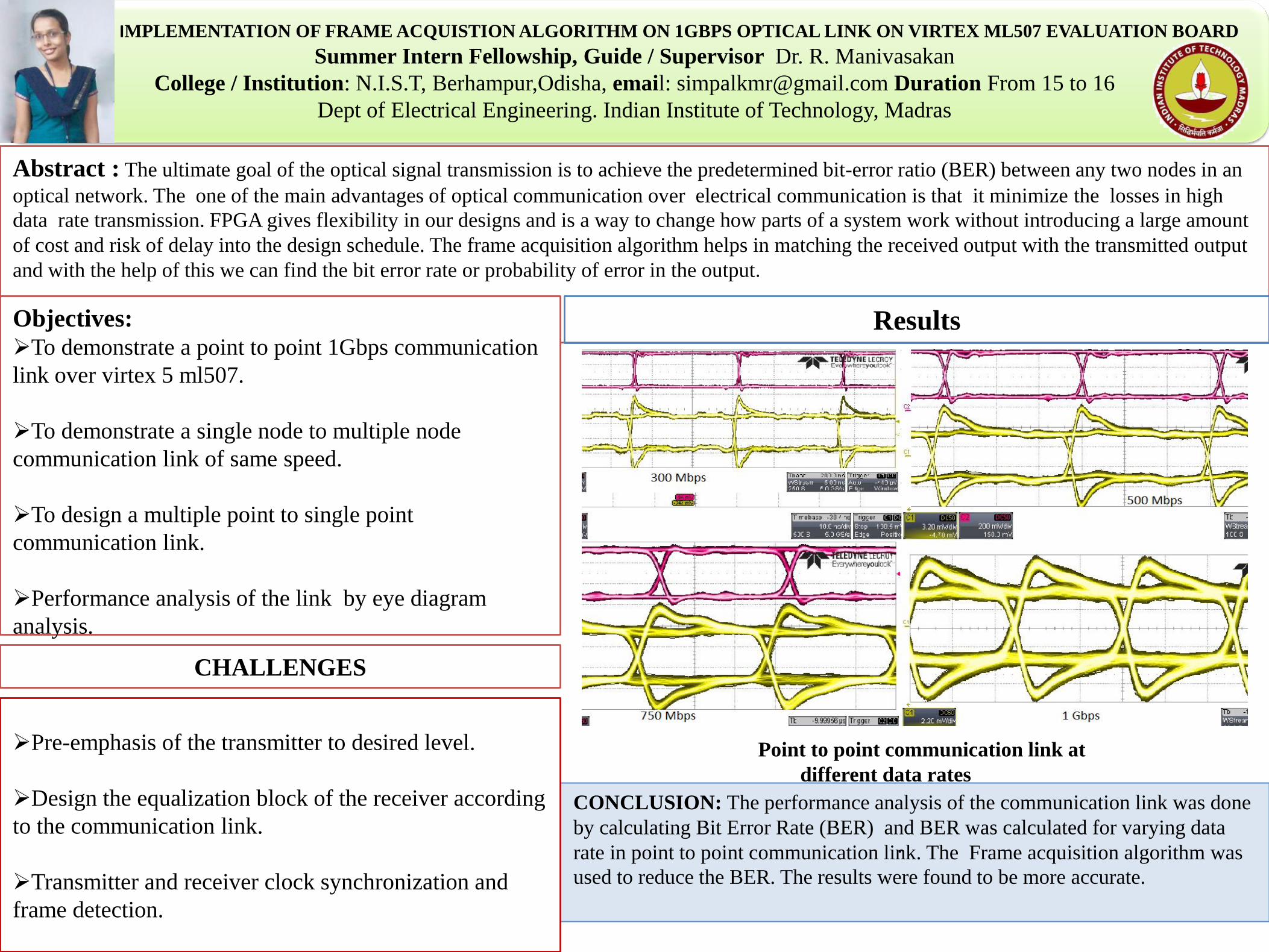
Results
CONCLUSION: The performance analysis of the communication link was done
by calculating Bit Error Rate (BER) and BER was calculated for varying data
rate in point to point communication link. The Frame acquisition algorithm was
used to reduce the BER. The results were found to be more accurate.
.
Point to point communication link at
different data rates
Pre-emphasis of the transmitter to desired level.
Design the equalization block of the receiver according
to the communication link.
Transmitter and receiver clock synchronization and
frame detection.

Simulation of thulium doped double clad fiber lasers submitted by Anandhi.C.A(EE15SFP0420)
under the guidance of Dr. Deepa Venkitesh
Model used in the simulation
Pump combiner
Pump input
(793 nm)
output
10 m
TDF
Experimental setup
COMPARISON OF SIMULATION AND EXPERIMENTAL RESULTS
Forward ASE spectrum Backward ASE spectrum
Pump
power=0.674W
Variation of ASE power as a function of pump power
Backward
ASE
Forward ASE
Spectroscopy of thulium doped silica system is studied and the simulations are done using RP Fiber Power. Some of the important
results are shown .
Transition cross-sections
used in the simulation
Backward ASE
Pump
power=3.43W
Related Documents