www.tjprc.org [email protected] DESIGN OF LOW POWER AND AREA EFFICIENT FULL ADDER FOR ALU USING 90NM PROCESS FOR INDUSTRIAL BASED CAD/CAM MANUFACTURING UNITS HARIHARAN K 1 ,RAAJAN N. R 2 , MANIKANDAN. R 3 & SEKAR K. R 4 1, 3, 4 Assistant Professor, School of Computing, SASTRA University Thanjavur, Tamil Nadu, India 2 Senior Assistant Professor, SEEE, SASTRA University Thanjavur, Tamil Nadu, India ABSTRACT This paper presents a high drivability of full adder with less area and power consumption. This GDI based full adder is implemented, by using both gate diffusion input (GDI) technique and pass transistor logic, that leads to be a reduced area and power. To reducing the static power, ultralow power diode (ULPD) is used. The leakage current of this diode, lies within the range of pA. The comparison has been done between existing systems like CMOS, CPL and hybrid full adders, with proposed full adder. All full adders are designed with gpdk 0.90 um, in Cadence Virtuoso schematic, and simulations are done in a Spectre Simulator. KEYWORDS: GDI Technique, UPLD, Hybrid Full Adder, CMOS & CPL Received: Sep 19, 2017; Accepted: Oct 09, 2017; Published: Oct 30, 2017; Paper Id: IJMPERDDEC20177 INTRODUCTION The adder is a basic building block [1-4], too many digital circuits like a digital signal processor (DSP), microprocessor, and also, it plays the major role in array multiplier to add partial products. In arithmetic unit binary addition plays the major role because every arithmetic operation is performed by using an addition operation. So building low power and high performance adders would affect the system performance and also reduce the whole power consumption. That’s why; to achieving its performance is crucial, to improving the whole circuit performance. The proposed full adder is designed with a minimum number of transistors, it causes the low power consumption and also less area. REVIEW OF DIFFERENT FULL ADDER TECHNOLOGIES In recent years, there are so many logic styles have been proposed to implement 1-bit full adder cells. The full adders are mainly classified into two types, one is static and another one is dynamic full adders. Static full adders consume less power than the dynamic full adders, because dynamic logic is a clocked logic. For N-input module, static requires 2N transistors and dynamic requires N+2 transistors. The advantage of using dynamic logic is faster, switching speed and less static power dissipation. By combining both logic styles we can achieve hybrid logic style with high performance. We can achieve low area and power, by combining two or more logic styles in a single circuit. CMOS Full Adder The static CMOS full adder follows the regular CMOS structure [5-6], it usually contains one PMOS pull- up network and one NMOS pull-down network, as shown in Figure 1. Original Article International Journal of Mechanical and Production Engineering Research and Development (IJMPERD) ISSN (P): 2249-6890; ISSN (E): 2249-8001 Vol. 7, Issue 6, Dec 2017, 71-80 © TJPRC Pvt. Ltd.

Welcome message from author
This document is posted to help you gain knowledge. Please leave a comment to let me know what you think about it! Share it to your friends and learn new things together.
Transcript
www.tjprc.org [email protected]
DESIGN OF LOW POWER AND AREA EFFICIENT FULL ADDER FOR ALU USING
90NM PROCESS FOR INDUSTRIAL BASED CAD/CAM MANUFACTURING UNITS
HARIHARAN K1 ,RAAJAN N. R
2, MANIKANDAN. R
3 & SEKAR K. R
4
1, 3, 4 Assistant Professor, School of Computing, SASTRA University Thanjavur, Tamil Nadu, India
2Senior Assistant Professor, SEEE, SASTRA University Thanjavur, Tamil Nadu, India
ABSTRACT
This paper presents a high drivability of full adder with less area and power consumption. This GDI based full
adder is implemented, by using both gate diffusion input (GDI) technique and pass transistor logic, that leads to be a
reduced area and power. To reducing the static power, ultralow power diode (ULPD) is used. The leakage current of this
diode, lies within the range of pA. The comparison has been done between existing systems like CMOS, CPL and hybrid
full adders, with proposed full adder. All full adders are designed with gpdk 0.90 um, in Cadence Virtuoso schematic, and
simulations are done in a Spectre Simulator.
KEYWORDS: GDI Technique, UPLD, Hybrid Full Adder, CMOS & CPL
Received: Sep 19, 2017; Accepted: Oct 09, 2017; Published: Oct 30, 2017; Paper Id: IJMPERDDEC20177
INTRODUCTION
The adder is a basic building block [1-4], too many digital circuits like a digital signal processor (DSP),
microprocessor, and also, it plays the major role in array multiplier to add partial products. In arithmetic unit binary
addition plays the major role because every arithmetic operation is performed by using an addition operation. So
building low power and high performance adders would affect the system performance and also reduce the whole
power consumption. That’s why; to achieving its performance is crucial, to improving the whole circuit
performance. The proposed full adder is designed with a minimum number of transistors, it causes the low power
consumption and also less area.
REVIEW OF DIFFERENT FULL ADDER TECHNOLOGIES
In recent years, there are so many logic styles have been proposed to implement 1-bit full adder cells.
The full adders are mainly classified into two types, one is static and another one is dynamic full adders. Static full
adders consume less power than the dynamic full adders, because dynamic logic is a clocked logic. For N-input
module, static requires 2N transistors and dynamic requires N+2 transistors. The advantage of using dynamic logic
is faster, switching speed and less static power dissipation. By combining both logic styles we can achieve hybrid
logic style with high performance. We can achieve low area and power, by combining two or more logic styles in a
single circuit.
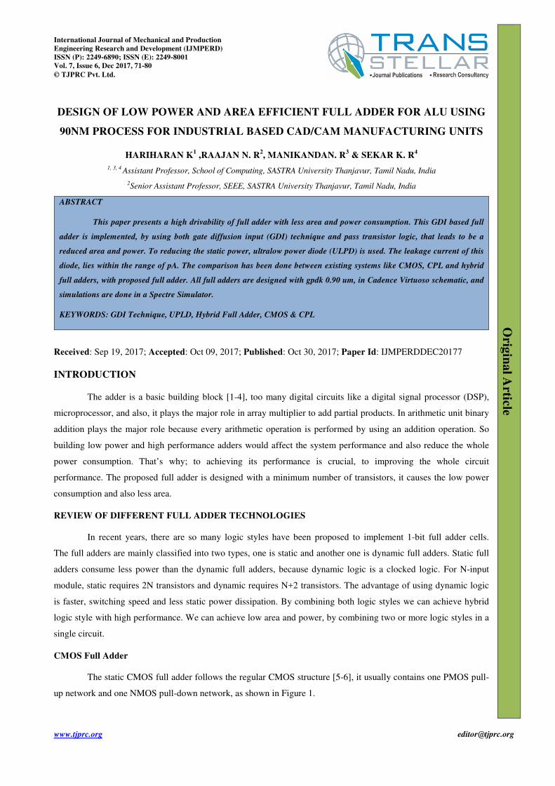
CMOS Full Adder
The static CMOS full adder follows the regular CMOS structure [5-6], it usually contains one PMOS pull-
up network and one NMOS pull-down network, as shown in Figure 1.
Orig
inal A
rtic
le International Journal of Mechanical and Production
Engineering Research and Development (IJMPERD)
ISSN (P): 2249-6890; ISSN (E): 2249-8001
Vol. 7, Issue 6, Dec 2017, 71-80
© TJPRC Pvt. Ltd.
72 Hariharan,K ,Raajan N.R,Manikandan.R & Sekar K.R
www.tjprc.org [email protected]
Figure 1: C-CMOS Full Adder
Schematic Diagram of C-Cmos Full Adder in 180nm Technology using Cadence
In complementary CMOS logic, the same function is performing two times; it may cause increasing of area and
power. The advantage of complementary CMOS style is its robustness, against voltage scaling and transistor sizing, which
are essential to provide reliable operation at low voltage with arbitrary transistor size. The disadvantage is driving
capability of the circuit is reduced by connecting transistors are in series, at the output stage. For suitable rectification
buffers are required. Another design style in CMOS is pass transistor logic (PTL) [7, 8]. There are two pass transistor
networks, one is PMOS, and another one is NMOS networks. Any one of the pass transistor networks is adequate to design
the given logic function. It requires less number of transistors than the CMOS full adder.
Manufacturing Methods Based on Production Quantity
Product Cycle in Conventional Manufacturing Environment
Design of Low Power and Area Efficient Full Adder for ALU Using 90nm 73
Process for Industrial Based CAD/CAM Manufacturing Units
Impact Factor (JCC): 6.8765 NAAS Rating: 3.11
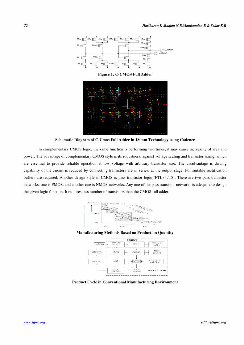
CPL Full Adder
The CPL circuits are designed, by using NMOS pass transistor network with CMOS inverters, at the output stage.
The CPL differs from pass transistor logic because source terminal of the pass transistor is not connected to either power
supply or ground. It is connected to any one input, the block diagram of a full adder using CPL, as shown in Figure-2.
The number of transistors to design CPL full adder is less than the CMOS full adder.
Figure 2: CPL Full Adder
Schematic Diagram of CPL Full Adder in 90nm Technology Using Cadence
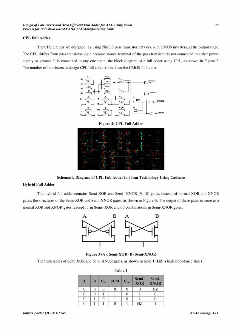
Hybrid Full Adder
This hybrid full adder contains Semi-XOR and Semi- XNOR [9, 10] gates, instead of normal XOR and XNOR
gates, the structures of the Semi-XOR and Semi-XNOR gates, as shown in Figure-3. The output of these gates is same as a
normal XOR and XNOR gates, except 11 in Semi- XOR and 00 combinations in Semi-XNOR gates.
Figure 3 (A): Semi-XOR (B) Semi-XNOR
The truth tables of Semi XOR and Semi XNOR gates, as shown in table 1 (HZ is high impedance state)
Table 1
A B Cin SUM Cout Semi-
XOR
Semi-
XNOR
0 0 0 0 0 0 HZ
0 0 1 1 0 1 0
0 1 0 1 0 1 0
0 1 1 0 1 HZ 1
74 Hariharan,K ,Raajan N.R,Manikandan.R & Sekar K.R
www.tjprc.org [email protected]
Table 1: contd.,
1 0 0 1 0 0 HZ
1 0 1 0 1 1 0
1 1 0 0 1 1 0
1 1 1 1 1 HZ 1
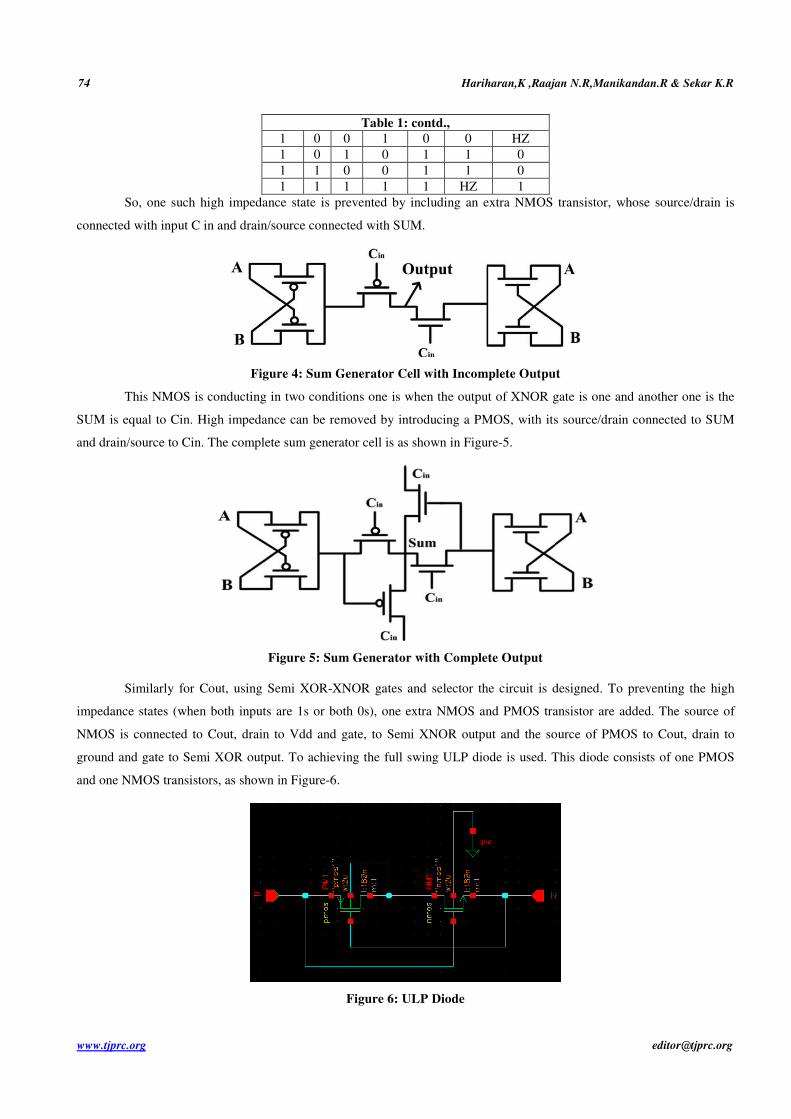
So, one such high impedance state is prevented by including an extra NMOS transistor, whose source/drain is
connected with input C in and drain/source connected with SUM.
Figure 4: Sum Generator Cell with Incomplete Output
This NMOS is conducting in two conditions one is when the output of XNOR gate is one and another one is the
SUM is equal to Cin. High impedance can be removed by introducing a PMOS, with its source/drain connected to SUM
and drain/source to Cin. The complete sum generator cell is as shown in Figure-5.
Figure 5: Sum Generator with Complete Output
Similarly for Cout, using Semi XOR-XNOR gates and selector the circuit is designed. To preventing the high
impedance states (when both inputs are 1s or both 0s), one extra NMOS and PMOS transistor are added. The source of
NMOS is connected to Cout, drain to Vdd and gate, to Semi XNOR output and the source of PMOS to Cout, drain to
ground and gate to Semi XOR output. To achieving the full swing ULP diode is used. This diode consists of one PMOS
and one NMOS transistors, as shown in Figure-6.
Figure 6: ULP Diode
Design of Low Power and Area Efficient Full Adder for ALU Using 90nm 75
Process for Industrial Based CAD/CAM Manufacturing Units
Impact Factor (JCC): 6.8765 NAAS Rating: 3.11
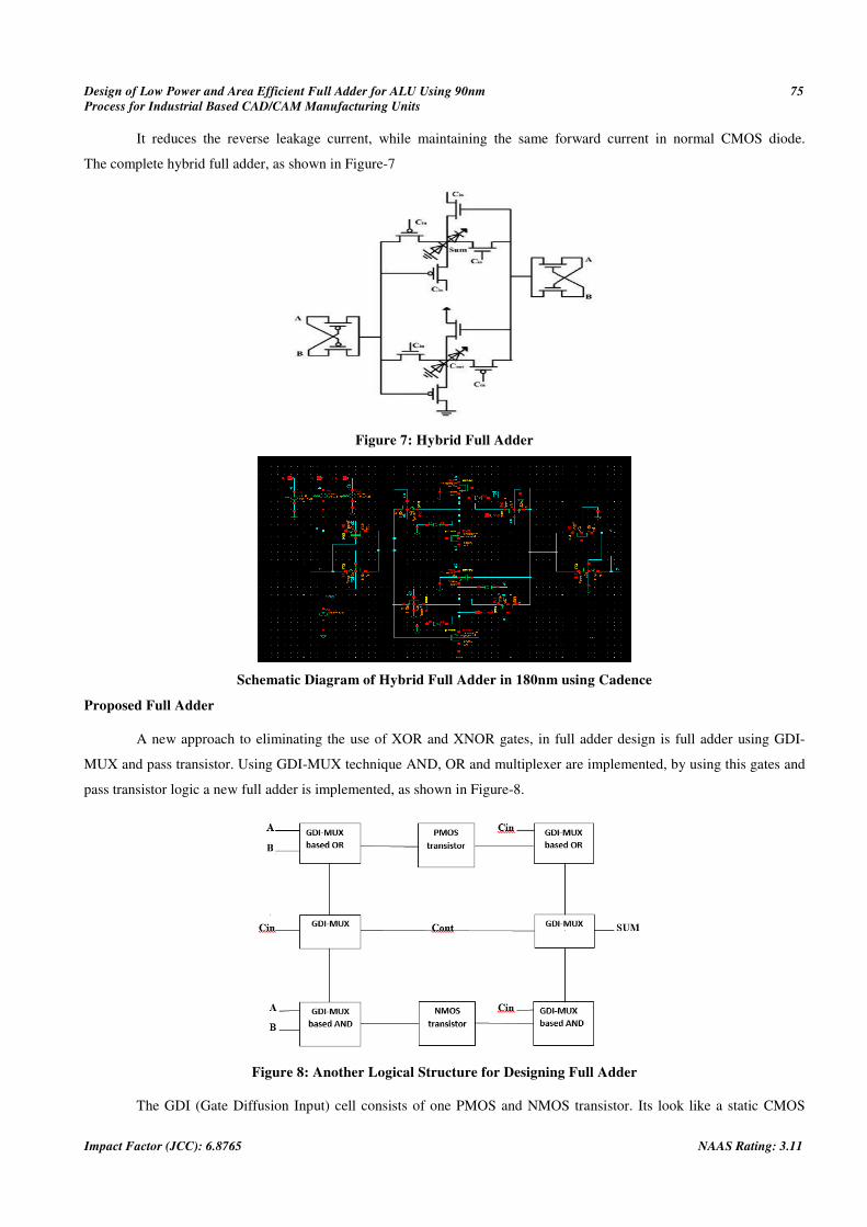
It reduces the reverse leakage current, while maintaining the same forward current in normal CMOS diode.
The complete hybrid full adder, as shown in Figure-7
Figure 7: Hybrid Full Adder
Schematic Diagram of Hybrid Full Adder in 180nm using Cadence
Proposed Full Adder
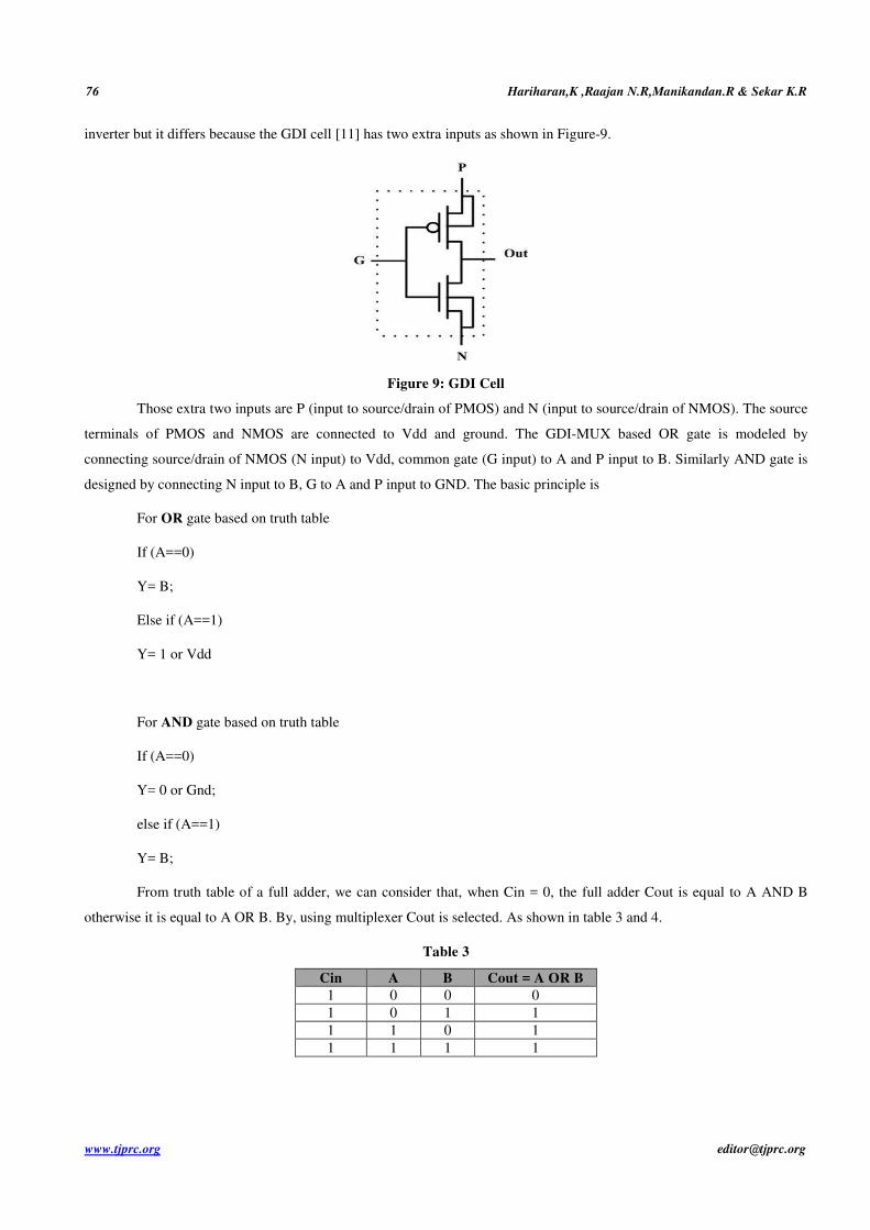
A new approach to eliminating the use of XOR and XNOR gates, in full adder design is full adder using GDI-
MUX and pass transistor. Using GDI-MUX technique AND, OR and multiplexer are implemented, by using this gates and
pass transistor logic a new full adder is implemented, as shown in Figure-8.
Figure 8: Another Logical Structure for Designing Full Adder
The GDI (Gate Diffusion Input) cell consists of one PMOS and NMOS transistor. Its look like a static CMOS
76 Hariharan,K ,Raajan N.R,Manikandan.R & Sekar K.R
www.tjprc.org [email protected]
inverter but it differs because the GDI cell [11] has two extra inputs as shown in Figure-9.
Figure 9: GDI Cell
Those extra two inputs are P (input to source/drain of PMOS) and N (input to source/drain of NMOS). The source
terminals of PMOS and NMOS are connected to Vdd and ground. The GDI-MUX based OR gate is modeled by
connecting source/drain of NMOS (N input) to Vdd, common gate (G input) to A and P input to B. Similarly AND gate is
designed by connecting N input to B, G to A and P input to GND. The basic principle is
For OR gate based on truth table
If (A==0)
Y= B;
Else if (A==1)
Y= 1 or Vdd
For AND gate based on truth table
If (A==0)
Y= 0 or Gnd;
else if (A==1)
Y= B;
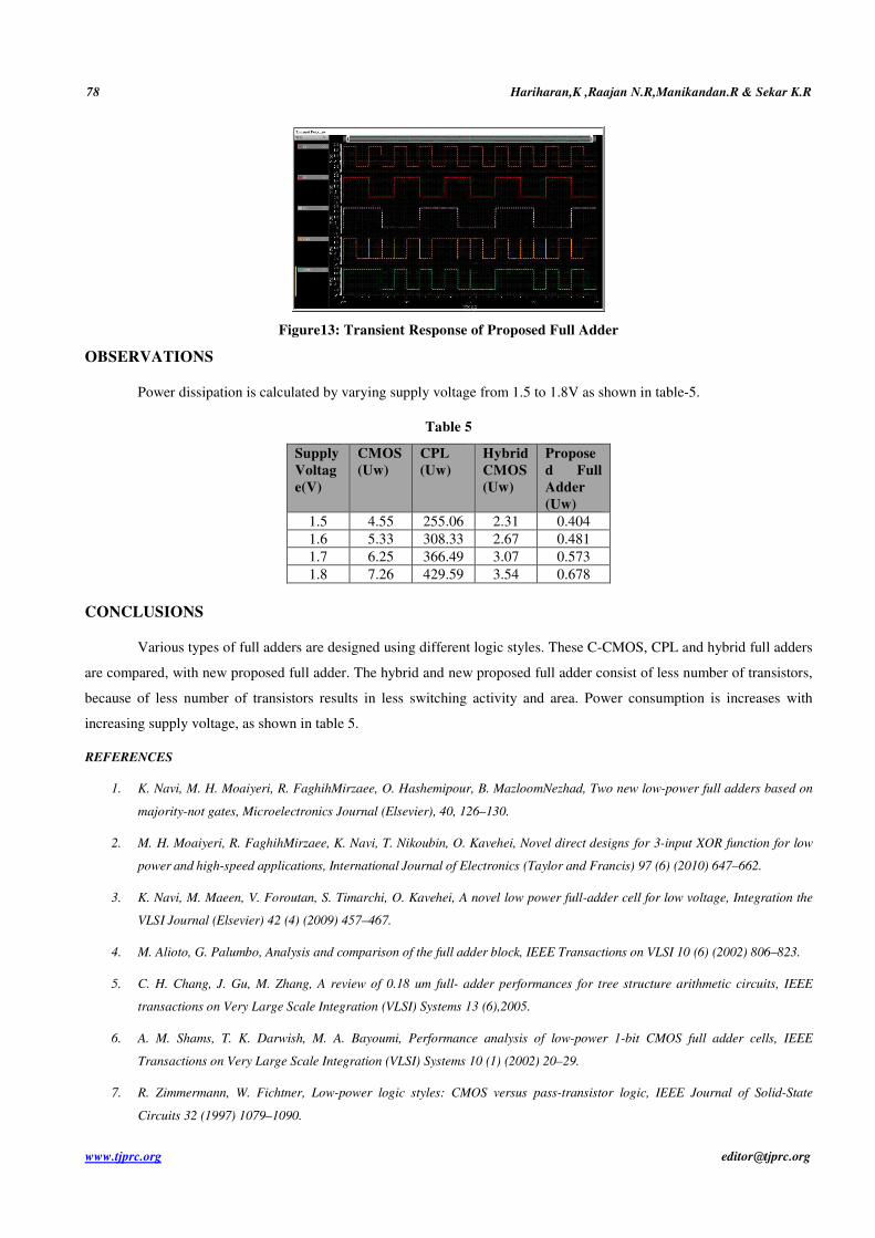
From truth table of a full adder, we can consider that, when Cin = 0, the full adder Cout is equal to A AND B
otherwise it is equal to A OR B. By, using multiplexer Cout is selected. As shown in table 3 and 4.
Table 3
Cin A B Cout = A OR B
1 0 0 0
1 0 1 1
1 1 0 1
1 1 1 1
Design of Low Power and Area Efficient Full Adder for ALU Using 90nm 77
Process for Industrial Based CAD/CAM Manufacturing Units
Impact Factor (JCC): 6.8765 NAAS Rating: 3.11
Table 4
Cin A B Cout = A AND B
0 0 0 0
0 0 1 0
0 1 0 0
0 1 1 1
When Cout = 0, the sum is equal A OR B OR Cin, otherwise sum is equal to A AND B AND Cin. The width and
length ratio of PMOS and NMOS transistor, in first GDI-MUX and second GDI-MUX, based AND gate is 200n:90n.
To achieving the full swing the width and length ratio is changed. And, also the PMOS and NMOS pass transistors are
added.
SIMULATION AND RESULTS
All full adders are designed and simulated by using a Cadence Virtuoso in 90nm gpdk CMOS technology. Power
dissipation is measured for different design techniques by varying voltage from 1.5 to 1.8V. The transient response of
different full adders, as shown in Figure-10 to Figure-1.
Figure10: Transient Response of C-CMOS Full Adder
Figure11: Transient Response of CPL Full Adder
Figure12: Transient Response of Hybrid Full Adder
78 Hariharan,K ,Raajan N.R,Manikandan.R & Sekar K.R
www.tjprc.org [email protected]
Figure13: Transient Response of Proposed Full Adder
OBSERVATIONS
Power dissipation is calculated by varying supply voltage from 1.5 to 1.8V as shown in table-5.
Table 5
Supply
Voltag
e(V)
CMOS
(Uw)
CPL
(Uw)
Hybrid
CMOS
(Uw)
Propose
d Full
Adder
(Uw)
1.5 4.55 255.06 2.31 0.404
1.6 5.33 308.33 2.67 0.481
1.7 6.25 366.49 3.07 0.573
1.8 7.26 429.59 3.54 0.678
CONCLUSIONS
Various types of full adders are designed using different logic styles. These C-CMOS, CPL and hybrid full adders
are compared, with new proposed full adder. The hybrid and new proposed full adder consist of less number of transistors,
because of less number of transistors results in less switching activity and area. Power consumption is increases with
increasing supply voltage, as shown in table 5.
REFERENCES
1. K. Navi, M. H. Moaiyeri, R. FaghihMirzaee, O. Hashemipour, B. MazloomNezhad, Two new low-power full adders based on
majority-not gates, Microelectronics Journal (Elsevier), 40, 126–130.
2. M. H. Moaiyeri, R. FaghihMirzaee, K. Navi, T. Nikoubin, O. Kavehei, Novel direct designs for 3-input XOR function for low
power and high-speed applications, International Journal of Electronics (Taylor and Francis) 97 (6) (2010) 647–662.
3. K. Navi, M. Maeen, V. Foroutan, S. Timarchi, O. Kavehei, A novel low power full-adder cell for low voltage, Integration the
VLSI Journal (Elsevier) 42 (4) (2009) 457–467.
4. M. Alioto, G. Palumbo, Analysis and comparison of the full adder block, IEEE Transactions on VLSI 10 (6) (2002) 806–823.
5. C. H. Chang, J. Gu, M. Zhang, A review of 0.18 um full- adder performances for tree structure arithmetic circuits, IEEE
transactions on Very Large Scale Integration (VLSI) Systems 13 (6),2005.
6. A. M. Shams, T. K. Darwish, M. A. Bayoumi, Performance analysis of low-power 1-bit CMOS full adder cells, IEEE
Transactions on Very Large Scale Integration (VLSI) Systems 10 (1) (2002) 20–29.
7. R. Zimmermann, W. Fichtner, Low-power logic styles: CMOS versus pass-transistor logic, IEEE Journal of Solid-State
Circuits 32 (1997) 1079–1090.

Design of Low Power and Area Efficient Full Adder for ALU Using 90nm 79
Process for Industrial Based CAD/CAM Manufacturing Units
Impact Factor (JCC): 6.8765 NAAS Rating: 3.11
8. D. Radhakrishnan, S. R. Whitaker, and G. K. Maki, “Formal design procedures for pass-transistor switching circuits,” IEEE
Journal of Solid-State Circuits, vol. 20, no. 2, pp. 531–536, 1984
9. J.-M. Wang, S.-C. Fang, W.-S. Feng, New efficient designs for XOR and XNOR functions on the transistor level, IEEE Journal
of Solid-State Circuits 29 (7) (1994) 780-786.
10. Foroutan, Vahid, MohammadRez Taheri, Keivan Navi, and Arash Azizi Mazreah, “ Design of two Low-Power full adder cells
using GDI structure and hybris CMOS logic style”, Integration the VLSI Journal, 2013.
11. Arkadiy Morgenshtein, A. Fish, Israel A. Wagner, Gate-diffusion input (GDI): a power-efficient method for digital
combinatorial circuits, IEEE Transactions on VLSI Systems (2002) 566–581.

Related Documents


