* This document contains certain information on a new product. Specifications and information herein are subject to change without notice. Document Number: MC33SA0528 Rev. 3.0, 7/2016 NXP Semiconductors Data sheet: Advance Information © 2016 NXP B.V. Dual DSI master transceiver The 33SA0528 is a third generation SMARTMOS standalone, dual-channel distributed system interface (DSI) master device. Each of the two independent channels contain a differential driver and a dual adder receiver. The embedded DSI protocol engine converts the DSI data between the physical interface and the two redundant SPI interfaces. The MCU can control and configure the 33SA0528 and extract all of the slaves transceivers data from it via the dual SPI. To ensure the communication reliability, the 33SA0528 uses an on-chip band gap reference regulator to monitor all of the supply voltages, and uses an on- chip oscillator to monitor the PLL clock for the external clock error detection. Features • Two independent DSI master channels • Supports command and response mode for slave configuration • Supports periodic data collection mode (PDCM) for periodic slave data transfers • Supports discovery mode for slave physical address self-programming • 10 MHz 32-bit dual SPI: main SPI for device configuration and DSI operation, and redundant SPI for safety purposes • Point-to-point, parallel, daisy chain bus topologies • Various diagnostic features Figure 1. 33SA0528 simplified application diagram Automotive restraint system 33SA0528 AC SUFFIX (PB-FREE) 98ASH70029A 32-PIN LQFP Applications • Automotive airbag and safety • Industrial systems • Sense and trigger applications 33SA0528 VDSI VCC5 SCK0 CS0B_D CLK_IN RSTB GNDSUB V2P5A V2P5D MOSI0 MISO0 SCK1 CS1B MOSI1 MISO1 CLK_OUT MCU SPI0_SCK SPI0_CS GPIO SPI0_MOSI SPI0_MISO SPI1_SCK SPI1_CS SPI1_MOSI SPI1_MISO V CC5 V DSI CLK CLKOUT DSI Slaves Interfaces GNDA GNDD GNDP_DSI0 GNDP_DSI1 DH0 DL0 DH1 DL1

Welcome message from author
This document is posted to help you gain knowledge. Please leave a comment to let me know what you think about it! Share it to your friends and learn new things together.
Transcript

Document Number: MC33SA0528Rev. 3.0, 7/2016
NXP Semiconductors Data sheet: Advance Information
Dual DSI master transceiverThe 33SA0528 is a third generation SMARTMOS standalone, dual-channel distributed system interface (DSI) master device.
Each of the two independent channels contain a differential driver and a dual adder receiver. The embedded DSI protocol engine converts the DSI data between the physical interface and the two redundant SPI interfaces. The MCU can control and configure the 33SA0528 and extract all of the slaves transceivers data from it via the dual SPI.
To ensure the communication reliability, the 33SA0528 uses an on-chip band gap reference regulator to monitor all of the supply voltages, and uses an on-chip oscillator to monitor the PLL clock for the external clock error detection.
Features
• Two independent DSI master channels• Supports command and response mode for slave configuration• Supports periodic data collection mode (PDCM) for periodic slave data
transfers• Supports discovery mode for slave physical address self-programming• 10 MHz 32-bit dual SPI: main SPI for device configuration and DSI operation,
and redundant SPI for safety purposes• Point-to-point, parallel, daisy chain bus topologies• Various diagnostic features
Figure 1. 33SA0528 simplified application diagram
Automotive restraint system
33SA0528
AC SUFFIX (PB-FREE)98ASH70029A32-PIN LQFP
Applications• Automotive airbag and safety• Industrial systems• Sense and trigger applications
33SA0528
VDSIVCC5
SCK0CS0B_D
CLK_IN
RSTB
GNDSUB
V2P5AV2P5D
MOSI0MISO0
SCK1CS1BMOSI1MISO1
CLK_OUT
MCU
SPI0_SCKSPI0_CS
GPIO
SPI0_MOSISPI0_MISO
SPI1_SCKSPI1_CS
SPI1_MOSISPI1_MISO
VCC5 VDSI
CLKCLKOUT
DSI Slaves InterfacesGNDAGNDD
GNDP_DSI0GNDP_DSI1
DH0DL0
DH1DL1
* This document contains certain information on a new product. Specifications and information herein are subject to change without notice.
© 2016 NXP B.V.
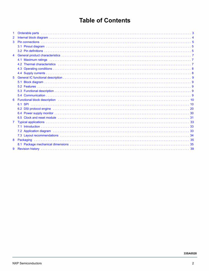
Table of Contents
1 Orderable parts . . . . . . . . . . . . . . . . . . . . . . . . . . . . . . . . . . . . . . . . . . . . . . . . . . . . . . . . . . . . . . . . . . . . . . . . . . . . . . . . . . . . . . . . 3
2 Internal block diagram . . . . . . . . . . . . . . . . . . . . . . . . . . . . . . . . . . . . . . . . . . . . . . . . . . . . . . . . . . . . . . . . . . . . . . . . . . . . . . . . . . . 4
3 Pin connections . . . . . . . . . . . . . . . . . . . . . . . . . . . . . . . . . . . . . . . . . . . . . . . . . . . . . . . . . . . . . . . . . . . . . . . . . . . . . . . . . . . . . . . . 5
3.1 Pinout diagram . . . . . . . . . . . . . . . . . . . . . . . . . . . . . . . . . . . . . . . . . . . . . . . . . . . . . . . . . . . . . . . . . . . . . . . . . . . . . . . . . . . . . 5
3.2 Pin definitions . . . . . . . . . . . . . . . . . . . . . . . . . . . . . . . . . . . . . . . . . . . . . . . . . . . . . . . . . . . . . . . . . . . . . . . . . . . . . . . . . . . . . . 5
4 General product characteristics . . . . . . . . . . . . . . . . . . . . . . . . . . . . . . . . . . . . . . . . . . . . . . . . . . . . . . . . . . . . . . . . . . . . . . . . . . . . 7
4.1 Maximum ratings . . . . . . . . . . . . . . . . . . . . . . . . . . . . . . . . . . . . . . . . . . . . . . . . . . . . . . . . . . . . . . . . . . . . . . . . . . . . . . . . . . . 7
4.2 Thermal characteristics . . . . . . . . . . . . . . . . . . . . . . . . . . . . . . . . . . . . . . . . . . . . . . . . . . . . . . . . . . . . . . . . . . . . . . . . . . . . . . 7
4.3 Operating conditions . . . . . . . . . . . . . . . . . . . . . . . . . . . . . . . . . . . . . . . . . . . . . . . . . . . . . . . . . . . . . . . . . . . . . . . . . . . . . . . . . 8
4.4 Supply currents . . . . . . . . . . . . . . . . . . . . . . . . . . . . . . . . . . . . . . . . . . . . . . . . . . . . . . . . . . . . . . . . . . . . . . . . . . . . . . . . . . . . . 8
5 General IC functional description . . . . . . . . . . . . . . . . . . . . . . . . . . . . . . . . . . . . . . . . . . . . . . . . . . . . . . . . . . . . . . . . . . . . . . . . . . . 9
5.1 Block diagram . . . . . . . . . . . . . . . . . . . . . . . . . . . . . . . . . . . . . . . . . . . . . . . . . . . . . . . . . . . . . . . . . . . . . . . . . . . . . . . . . . . . . . 9
5.2 Features . . . . . . . . . . . . . . . . . . . . . . . . . . . . . . . . . . . . . . . . . . . . . . . . . . . . . . . . . . . . . . . . . . . . . . . . . . . . . . . . . . . . . . . . . . 9
5.3 Functional description . . . . . . . . . . . . . . . . . . . . . . . . . . . . . . . . . . . . . . . . . . . . . . . . . . . . . . . . . . . . . . . . . . . . . . . . . . . . . . . . 9
5.4 Communication . . . . . . . . . . . . . . . . . . . . . . . . . . . . . . . . . . . . . . . . . . . . . . . . . . . . . . . . . . . . . . . . . . . . . . . . . . . . . . . . . . . . . 9
6 Functional block description . . . . . . . . . . . . . . . . . . . . . . . . . . . . . . . . . . . . . . . . . . . . . . . . . . . . . . . . . . . . . . . . . . . . . . . . . . . . . 10
6.1 SPI . . . . . . . . . . . . . . . . . . . . . . . . . . . . . . . . . . . . . . . . . . . . . . . . . . . . . . . . . . . . . . . . . . . . . . . . . . . . . . . . . . . . . . . . . . . . . 10
6.2 DSI protocol engine . . . . . . . . . . . . . . . . . . . . . . . . . . . . . . . . . . . . . . . . . . . . . . . . . . . . . . . . . . . . . . . . . . . . . . . . . . . . . . . . 20
6.4 Power supply monitor . . . . . . . . . . . . . . . . . . . . . . . . . . . . . . . . . . . . . . . . . . . . . . . . . . . . . . . . . . . . . . . . . . . . . . . . . . . . . . . 30
6.5 Clock and reset module . . . . . . . . . . . . . . . . . . . . . . . . . . . . . . . . . . . . . . . . . . . . . . . . . . . . . . . . . . . . . . . . . . . . . . . . . . . . . 31
7 Typical applications . . . . . . . . . . . . . . . . . . . . . . . . . . . . . . . . . . . . . . . . . . . . . . . . . . . . . . . . . . . . . . . . . . . . . . . . . . . . . . . . . . . . 33
7.1 Introduction . . . . . . . . . . . . . . . . . . . . . . . . . . . . . . . . . . . . . . . . . . . . . . . . . . . . . . . . . . . . . . . . . . . . . . . . . . . . . . . . . . . . . . . 33
7.2 Application diagram . . . . . . . . . . . . . . . . . . . . . . . . . . . . . . . . . . . . . . . . . . . . . . . . . . . . . . . . . . . . . . . . . . . . . . . . . . . . . . . . 33
7.3 Layout recommendations . . . . . . . . . . . . . . . . . . . . . . . . . . . . . . . . . . . . . . . . . . . . . . . . . . . . . . . . . . . . . . . . . . . . . . . . . . . . 34
8 Packaging . . . . . . . . . . . . . . . . . . . . . . . . . . . . . . . . . . . . . . . . . . . . . . . . . . . . . . . . . . . . . . . . . . . . . . . . . . . . . . . . . . . . . . . . . . . 35
8.1 Package mechanical dimensions . . . . . . . . . . . . . . . . . . . . . . . . . . . . . . . . . . . . . . . . . . . . . . . . . . . . . . . . . . . . . . . . . . . . . . 35
9 Revision history . . . . . . . . . . . . . . . . . . . . . . . . . . . . . . . . . . . . . . . . . . . . . . . . . . . . . . . . . . . . . . . . . . . . . . . . . . . . . . . . . . . . . . . 39
NXP Semiconductors 2
33SA0528

1 Orderable parts
This section describes the part numbers available to be purchased along with their differences.
Table 1. Orderable part variations
Part number Notes Temperature (TA) Package
MC33SA0528AC (1) -40 °C to 125 °C 32-PIN LQFP
Notes1. To order parts in tape & reel, add the R2 suffix to the part number.
3 NXP Semiconductors
33SA0528

2 Internal block diagram
Figure 2. 33SA0528 simplified internal block diagram
VDSI
VCC5
DH0
DL0
DH1
DL1
RSTB
CLK_IN
CS0B_DSCLK0MOSI0MISO0
GNDDGNDA
DS
I Pro
toco
l Eng
ine
SPI0_DRegisters
andState Machine
Receiver Sum1
Bus ReceiverBus DriverCurrent Limiter
TS
POR
Ch0 Driver/Receiver
Ch1 Driver/Receiver
Receiver Sum2
Adder
SPI1Registers
andState Machine
CS1BSCLK1MOSI1MISO1
CLK_OUTCLK Monitor
and PLL
V2P5AV2P5D
Voltage Supplies Monitors
Bandgap References
GNDP_DSI
Internal Voltages
NXP Semiconductors 4
33SA0528

3 Pin connections
3.1 Pinout diagram
Figure 3. 33SA0528 32-pin LQFP pinout diagram
3.2 Pin definitions
A functional description of each pin can be found in the functional pin description section beginning on page 9.
Table 2. 33SA0528 pin definitions
Pin number Pin name Pin function Definition
1 VDSI Power This supply input is used to provide the positive level output of buses
2 DH0 Output driver Bus 0 high-side
3 GND_DSI0 Ground Bus power return
4 DL0 Output driver Bus 0 low-side
5 GNDSUB Ground This pin must be tied to ground in the application.
6 DH1 Output driver Bus 1 high-side
7 GND_DSI1 Ground Bus power return
8 DL1 Output driver Bus 1 low-side
9 RSTB Reset A low level on this pin returns all registers to a known initial state.
10 SCK0 InputClocks data in from and out to DSI_SPI0. MISO0 data changes on the negative transition of SCLK0. MOSI0 is sampled on the positive edge of SCLK0
11 CS0B_D InputWhen this signal is high, SPI signals on DSI_SPI0 are ignored. Asserting this pin low starts a DSI_SPI0 transaction. The DSI_SPI0 transaction is signaled as completed when this signal returns high
12 SCK1 InputClocks data in from and out to DSI_SPI1. MISO1 data changes on the negative transition of SCLK1. MOSI1 is sampled on the positive edge of SCLK1
1
2
3
4
5
6
7
89 10 11 12 13 14 15 16
24
23
22
21
20
19
18
17
32 21 30 29 28 27 26 25VDSI
DH0
GNDP_DSI0
DL0
GNDSUB
DH1
GNDP_DSI1
DL1
RS
TB
SC
K0
CS
0B
_D
SC
K1
CS
1B
NC
MO
SI0
MO
SI1
MISO0
CLKOUT
MISO1
GNDSUB
CLKIN
NC
NC
NC
NC
GN
DA
V2
P5
A
V2
P5
D
NC
NC
VC
C5
GN
DD
5 NXP Semiconductors
33SA0528

13 CS1B InputWhen this signal is high, SPI signals on DSI_SPI1 are ignored. Asserting this pin low starts a DSI_SPI1 transaction. The DSI_SPI1 transaction is signaled as completed when this signal returns high
14 N.C — This pin is not internally connected and must be left unconnected or tied to ground in the application
15 MOSI0 Input SPI data into DSI_SPI0. This data input is sampled on the positive edge of SCLK0
16 MOSI1 Input SPI data into DSI_SPI1. This data input is sampled on the positive edge of SCLK1
17 N.C — This pin is not internally connected and must be left unconnected or tied to ground in the application
18 N.C — This pin is not internally connected and must be left unconnected or tied to ground in the application
19 N.C — This pin is not internally connected and must be left unconnected or tied to ground in the application
20 CLK_IN Input 4.0 MHz clock input
21 GNDSUB Ground This pin must be tied to ground in the application
22 MISO1 OutputDSI_SPI1 data sent to the MCU by this device. This data output changes on the negative edge of SCLK1. When CS1B_D is high, this pin is high
23 CLK_OUT Output Output buffered clock signal that is input from CLK_IN
24 MISO0 OutputDSI_SPI0 data sent to the MCU by this device. This data output changes on the negative edge of SCLK0. When CS0B_D is high, this pin is set at high impedance
25 GNDD Ground Ground for the digital circuits. Ground for IDDQ. This pin should be tied to MCU ground
26 VCC5 Power Regulated 5.0 V input
27 N.C — This pin is not internally connected and must be left unconnected or tied to ground in the application
28 N.C — This pin is not internally connected and must be left unconnected or tied to ground in the application
29 V2P5D Output 0.1 μF capacitor should be connected between this pin and ground
30 V2P5A Output 0.1 μF capacitor should be connected between this pin and ground
31 GNDA GroundGround for the analog circuits. This pin is not connected internally to the other grounds on the chip. It should be connected to a quiet ground on the board
32 N.C — This pin is not internally connected and must be left unconnected or tied to ground in the application
Table 2. 33SA0528 pin definitions(continued)
Pin number Pin name Pin function Definition
NXP Semiconductors 6
33SA0528

4 General product characteristics
4.1 Maximum ratings
4.2 Thermal characteristics
Table 3. Maximum ratings All voltages are with respect to ground unless otherwise noted. Exceeding these ratings may cause a malfunction or permanent damage to the device.
Symbol Description (rating) Min. Max. Unit Notes
Electrical ratings
VDSIDSI bus voltage supply
• Steady-state-0.3 10 V
VCC5 VCC logic supply voltage -0.3 7.0 V
V2P5A Regulated output voltage -0.3 3.0 V
V2P5D Regulated output voltage -0.3 3.0 V
VLOGIC Voltage on logic input/output pins -0.3 VCC5 + 3.0 V
ILOGIC Current on logic input/output pins — 20 mA
VBUS Voltage on DSI bus pins -0.3 20 V
IBUS Current on DSI bus pins — 200 mA
VESD
ESD voltage• Human body model (HBM)• Machine model (MM)• Charge device model (CDM)
———
±2000 ±150±500
V (2)
Notes2. ESD testing is performed in accordance with the human body model (HBM) (CZAP = 100 pF, RZAP = 1500 Ω), the machine model (MM)
(CZAP = 200 pF, RZAP = 0 Ω), and the charge device model.
Table 4. Thermal ratings All voltages are with respect to ground unless otherwise noted. Exceeding these ratings may cause a malfunction or permanent damage to the device.
Symbol Description (rating) Min. Max. Unit Notes
TATJ
Operating temperature• Ambient• Junction
-40-40
105150
°C
TSTG Storage temperature -55 150 °C
TSD Thermal shutdown (bus driver) 155 195 °C
7 NXP Semiconductors
33SA0528

4.3 Operating conditions
This section describes the operating conditions of the device. Conditions apply to all the following data, unless otherwise noted.
4.4 Supply currents
This section describes the current consumption characteristics of the device, as well as the conditions for the measurements.
Table 5. Operating conditions
All voltages are with respect to ground unless otherwise noted. Exceeding these ratings may cause a malfunction or permanent damage to the device.
Symbol Ratings Min. Max. Unit Notes
VDSI Full characteristics are guaranteed 9.0 9.6 V
VDSISome characteristics are out of specification, but the 33SA0528 can communicate with the bus slaves
8.8 9.0 V
VDSISome characteristics are out of specification, but the VDSI monitor is active, so the RNE bit is never set
8.2 8.8 V
VCC5 Functional operating VCC5 voltage 4.8 5.25 V
Table 6. Supply currents
All voltages are with respect to ground unless otherwise noted. Exceeding these ratings may cause a malfunction or permanent damage to the device. Typical values noted reflect the approximate parameter mean at TA = 25 °C.
Symbol Ratings Min. Typ. Max. Unit Notes
IVDSI
Current on DSI bus• 9.6 V (disabled)• 9.6 V (enabled 1.0 mA/channel)• 9.6 V (enabled 40 mA/channel)
8.0
18
96
11
24
108
13
30
114
mA (3)
IVCC Current on VCC5 supply — — 2.0 mA
Notes3. IOUT is the total current for all sensors connected to two DSI interfaces. For example: If 40 mA is flowing out (DHx to DLx) on each DSI channel,
then IOUT = 2 x 40 mA = 80 mA. The max. internal current flowing from VDSI to GND is ’28 mA + (80 mA/14) = 34 mA’. The max. total current is
flowing from VDSI (includes sensor current) is ’34 mA + 80 mA = 114 mA’. If the DSI channel-0 is enabled and 40 mA is flowing out (DHx to DLx), the other DSI channel (ch1) is the disabled case. The max. internal current flowing from VDSI to GND is ’19 mA + (40 mA/14) = 22 mA’. The Max. total current flowing from VDSI (include sensor current) is ’22 mA + 40 mA = 62 mA’.
NXP Semiconductors 8
33SA0528

5 General IC functional description
5.1 Block diagram
Figure 4. 33SA0528 functional block diagram
5.2 Features
• Main SPI at 10 MHz and 32-bit frame size provides access to all main registers• Redundant SPI with the same format provides access to redundant registers with slaves’ data, for safety purposes• DSI protocol engine provides two independent channels to communicate and decode up to eight sensors• Power supplies monitor detects and informs undervoltages on all four power pins (VDSI, VCC5, V2P5A, V2P5D)• Internal PLL block generates 10 MHz stable frequency from 4.0 Mhz input clock• Internal clock generator (no resonator) provides internal 4.0 MHz reference for clock frequency watchdog block• Clock monitor sets proper flags if any abnormality is detected in clock or PLL frequencies
5.3 Functional description
The 33SA0528 is a DSI master device behaving as an interface between the MCU and the DSI slaves connected to the system bus. It supports up to four slaves connected to each of the two available DSI channels, allowing for a total of eight slaves. The MCU can access the registers in the 33SA0528 via two independent SPIs, the first one being for configuration purposes and to interact with the DSI slaves. The second one provides full redundancy of slaves’ responses, which is designed for safety applications. The 33SA0528 can also act as a DSI Companion Chip when working together with a DSI SBC, expanding this last chip’s capacity regarding the maximum number of DSI slaves it can decode.
5.4 Communication
5.4.1 SPIBoth SPI channels share the same speed and format, so only one MCU configuration scheme is needed to communicate with the 33SA0528. The maximum frequency of this interface is clocked at 10 MHz and provided by the internal PLL, generated from the 4.0 MHz clock input. Each command follows a 32-bit format, with the 5th byte being optional. The SPI is in-command full-duplex, which means the 33SA0528 responds during the same SPI frame in which it demands to read a register, meaning the device can write or read any register in just one SPI command.
5.4.2 DSIThe 33SA0528 provides an interface for a DSI Differential bus, having two independent channels. Each channel can drive and decode up to four slaves connected in either point-to-point, parallel, or resistor-based daisy-chained bus. For each channel, the DSI Receiver block provides a doubled redundancy when composing the differential (high/send and low/return) values read from the bus, which makes this device is ideal for safety applications. For more information on the DSI protocol, refer to its consortium web site: http://www.dsiconsortium.org.
Main SPI Redundant SPI
DSI Protocol Engine
Power Supply Monitoring
Clock Monitoring and Reset
9 NXP Semiconductors
33SA0528

6 Functional block description
6.1 SPI
6.1.1 Block diagram
Figure 5. SPI modules pins and block diagram
6.1.2 Timings and configurationThe timings and commands format is the same for both SPI modules.
Figure 6. SPI modules timings
SPI0SCK0CS0B_DMOSI0MISO0
SPI1SCK1CS1BMOSI1MISO1
To MCU SPI0
To MCU SPI1
CSB
SCLK
MOSI
MISO
MSB LSBX
MSB LSBX
VIH
VIL
tCYC
tHI tLO
VIH
VILVIL
tLEAD tFtR
tSU tH
VOH
VOL
VIH
VIH
tLAG
tV tDIS
tNEG
NXP Semiconductors 10
33SA0528

6.1.3 Frame formatThe SPI module transactions start with a command and address byte and can be followed by three or four bytes of data. The start of a SPI transaction is signaled by the CSB signal being asserted low. The first bit sent (bit 7) of the first byte signals a read (bit = ‘0’) or write (bit = ‘1’) operation. The last seven bits (bit 6 to 0) of the first byte indicate the address of the desired register. Both 4-byte access and 5-byte access are valid for all register address. During a SPI transaction the 33SA0528 checks for SPI framing errors. A framing error is defined as any number of clocks received which is neither 32 nor 40. If this occurs, all bits sent by the SPI master are discarded and no registers are updated.
Figure 7. SPI module frames format - 4 byte access
Table 7. SPI modules timings
Symbol Parameter Min. Typ. Max. Unit Notes
tCYC SPI clock cycle time 99 — — ns
tHI SPI clock high time 40 — — ns
tLO SPI clock low time 40 — — ns
tLEAD SPI chip select lead time 50 — — ns
tLAG SPI chip select lag time 50 — — ns
tSUData setup time
• MOSI valid after SCK rising edge10 — — ns
tHData hold time
• MOSI valid after SCK rising edge10 — — ns
tVData valid time
• SCK falling edge to MISO valid, C = 50 pF— — 25 ns
tDISOutput disable time
• CSB rise to MISO high-impedance— — 50 ns
tRRise time (30% VCC to 70% VCC)
• SCK, MOSI— — 10 ns
tFFall time (70% VCC to 30% VCC)
• SCK, MOSI— — 10 ns
tNEG Chip select negate timer (read/write) 600 — — ns
Write/Read bit
REG ADDR
7 bits
DATA DATA DATA
1st byte 2nd byte 3rd byte 4th byteMOSI
N/A DATA DATA DATAMISO
SCK
CSB
11 NXP Semiconductors
33SA0528

Figure 8. SPI modules frames format - 5 bytes access
6.1.4 Register maps
Table 8. SPI0 register map
Address Name Type 2nd byte 3rd byte 4th byte 5th byte (optional)
0x00 CRM Tx/Rx Data Buffer D0 R/W D0DATA2 D0DATA1 D0DATA0 D0RES_STAT
0x01 CRM Tx/Rx Data Buffer D0 R D0DATA1 D0DATA0 D0RES_STAT —
0x02 PDCM Data Buffer D0R0 R D0R0DATA2 D0R0DATA1 D0R0DATA0 —
0x04 PDCM Data Buffer D0R1 R D0R1DATA2 D0R1DATA1 D0R1DATA0 —
0x06 PDCM Data Buffer D0R2 R D0R2DATA2 D0R2DATA1 D0R2DATA0 —
0x08 PDCM Data Buffer D0R3 R D0R3DATA2 D0R3DATA1 D0R3DATA0 —
0x0A PDCM Control D0 R/W D0PDCM_CTRL D0PDCM_DLY N/A —
0x0B Channel Control D0 R/W D0CTRL D0DPC D0STAT —
0x0C PDCM Configuration D0 R/W D0CHIP_TIME D0SID_R0R1 D0SID_R2R3 —
0x0E Channel Clear D0 R/W D0CLR N/A N/A —
0x10 CRM Tx/Rx Data Buffer D1 R/W D1DATA2 D1DATA1 D1DATA0 D1RES_STAT
0x11 CRM Tx/Rx Data Buffer D1 R D1DATA1 D1DATA0 D1RES_STAT —
0x12 PDCM Data Buffer D1R0 R D1R0DATA2 D1R0DATA1 D1R0DATA0 —
0x14 PDCM Data Buffer D1R1 R D1R1DATA2 D1R1DATA1 D1R1DATA0 —
0x16 PDCM Data Buffer D1R2 R D1R2DATA2 D1R2DATA1 D1R2DATA0 —
0x18 PDCM Data Buffer D1R3 R D1R3DATA2 D1R3DATA1 D1R3DATA0 —
0x1A PDCM Control D1 R/W D1PDCM_CTRL D1PDCM_DLY N/A —
0x1B Channel Control D1 R/W D1CTRL D1DPC D1STAT —
0x1C PDCM Configuration D1 R/W D1CHIP_TIME D1SID_R0R1 D1SID_R2R3 —
0x1E Channel Clear D1 R/W D1CLR N/A N/A —
0x40 NCKPTN R 0xAA 0xAA 0xAA —
0x41 CHKPTN R 0x55 0x55 0x55 —
0x42 MASKID R MASKID — — —
Notes4. Dn registers refer to the DSI channel n, so D0 corresponds to channel 0 and D1 corresponds to channel 1.5. Rm registers refer to the DSI slave addressed at m, so R0 corresponds to slave at address 0 and so on.6. The registers that correspond to different DSI channels and addresses have the same format and description.
Write/Read bit
REG ADDR
7 bits
DATA DATA DATA DATA
1st byte 2nd byte 3rd byte 4th byte 5th byteMOSI
N/A DATA DATA DATA DATA
5th byte is only available for SPI0 registers 0x00 and 0x10
MISO
SCK
CSB
NXP Semiconductors 12
33SA0528

6.1.5 Registers description
6.1.5.1 CRM Tx/Rx data buffer Dn
Table 9. SPI1 register map
Address Name Type 2nd byte 3rd byte 4th byte 5th byte (optional)
0x02 PDCM Data Buffer D0R0 R D0R0DATA2 D0R0DATA1 D0R0DATA0 -
0x04 PDCM Data Buffer D0R1 R D0R1DATA2 D0R1DATA1 D0R1DATA0 -
0x06 PDCM Data Buffer D0R2 R D0R2DATA2 D0R2DATA1 D0R2DATA0 -
0x08 PDCM Data Buffer D0R3 R D0R3DATA2 D0R3DATA1 D0R3DATA0 -
0x12 PDCM Data Buffer D1R0 R D1R0DATA2 D1R0DATA1 D1R0DATA0 -
0x14 PDCM Data Buffer D1R1 R D1R1DATA2 D1R1DATA1 D1R1DATA0 -
0x16 PDCM Data Buffer D1R2 R D1R2DATA2 D1R2DATA1 D1R2DATA0 -
0x18 PDCM Data Buffer D1R3 R D1R3DATA2 D1R3DATA1 D1R3DATA0 -
0x40 NCKPTN R 0xAA 0xAA 0xAA -
0x41 CHKPTN R 0x55 0x55 0x55 -
Notes
• These registers have the same format and description as their SPI0 counterparts, as they are just for redundancy purposes.
Table 10. 2nd byte - DnDATA2
Bit 7 6 5 4 3 2 1 0
RDnDATA[23] DnDATA[22] DnDATA[21] DnDATA[20] DnDATA[19] DnDATA[18] DnDATA[17] DnDATA[16]
W
Reset 0 0 0 0 0 0 0 0
Table 11. 3rd byte - DnDATA1
Bit 7 6 5 4 3 2 1 0
RDnDATA[15] DnDATA[14] DnDATA[13] DnDATA[12] DnDATA[11] DnDATA[10] DnDATA[9] DnDATA[8]
W
Reset 0 0 0 0 0 0 0 0
Table 12. 4th byte - DnDATA
Bit 7 6 5 4 3 2 1 0
RDnDATA[7] DnDATA[6] DnDATA[5] DnDATA[4] DnDATA[3] DnDATA[2] DnDATA[1] DnDATA[0]
W
Reset 0 0 0 0 0 0 0 0
Table 13. 5th byte - DnRES_STAT
Bit 7 6 5 4 3 2 1 0
R ER - - UV TE RNE 0 1
13 NXP Semiconductors
33SA0528

6.1.5.2 PDCM data buffer DnRm
W
Reset 0 0 0 0 1 0 0 1
Table 14. CRM Tx/Rx data buffer Dn fields description
Field Description
DnDATA[23:0]CRM data to transmit or CRM data received from slavesIf the DSI channel EN bit is set, and the 33SA0528 is not in PDCM, data is transmitted after being written to the register. Also, slaves’ CRM data is written back to the buffer as soon as it is received through the bus.
ERError bitThis bit indicates, for received data, there is either a CRC error, an undefined symbol error, or data mismatch between the dual DSI receivers.
UVUndervoltageThis bit indicates VDSI dropped below its minimum threshold for a specified time. Refer to Power supply monitor on page 30.
TETransmit emptyThis bit indicates there is no data in the transmit buffer.
RNEReceiver not emptyThis bit indicates there is data available that has been received from the slaves.
Table 15. 2nd byte - DnRmDATA2
Bit 7 6 5 4 3 2 1 0
R ER - RNE UV DnRmData[19] DnRmData[18] DnRmData[17] DnRmData[16]
W
Reset 0 0 0 0 0 0 0 0
Table 16. 3rd byte - DnRmDATA1
Bit 7 6 5 4 3 2 1 0
R DnRmData[15] DnRmData[14] DnRmData[13] DnRmData[12] DnRmData[11] DnRmData[10] DnRmData[9] DnRmData[8]
W
Reset 0 0 0 0 0 0 0 0
Table 17. 4th byte - DnRmDATA0
Bit 7 6 5 4 3 2 1 0
R DnRmData[7] DnRmData[6] DnRmData[5] DnRmData[4] DnRmData[3] DnRmData[2] DnRmData[1] DnRmData[0]
W
Reset 0 0 0 0 0 0 0 0
Table 13. 5th byte - DnRES_STAT
Bit 7 6 5 4 3 2 1 0
NXP Semiconductors 14
33SA0528

6.1.5.3 PDCM control Dn
Table 18. PDCM data buffer DnRm fields description
Field Description
DnRmDATA[19:0]PDCM data received from slavesDnRmDATA[19:16] represent the source ID field of the slave, and it is used as seed for CRC calculation.
ERError bitThis bit indicates, for received data, that there is either a CRC error, an undefined symbol error, or data mismatch between the dual DSI receivers.
UVUndervoltageThis bit indicates VDSI dropped below its minimum threshold for a specified time. Refer to Power supply monitor on page 30.
RNEReceiver not emptyThis bit indicates there is data available that has been received from the slaves.
Table 19. 2nd byte - DnPDCM_CTRL
Bit 7 6 5 4 3 2 1 0
RDnBRC - - - - - DnAUTO DnPDCM_EN
W
Reset 0 0 0 0 0 0 0 0
Table 20. 3rd byte - DnPDCM_DLY
Bit 7 6 5 4 3 2 1 0
RDELAY[7] DELAY[6] DELAY[5] DELAY[4] DELAY[3] DELAY[2] DELAY[1] DELAY[0]
W
Reset 0 0 0 0 0 0 0 0
Table 21. PDCM control Dn fields description
Field Description
DnBRCBroadcast read commandEach time this bit is set, a manual BRC is transmitted through the DSI bus. Only valid when DnPDCM_EN is 1 and DnAUTO is 0.
DnAUTOAutomatic BRCWhen this bit is set, a BRC is transmitted automatically through the DSI bus every 500 µs. Write access to this bit is ignored when DnPDCM_EN is 0.
DnPDCM_ENPeriodic data collection mode enableOnce this bit is set, the 33SA0528 enters PDCM, preventing any CRM communication or any configuration change. This bit can be cleared by clearing the channel, by writing to the channel clear Dn register.
DELAY[7:0]Broadcast read command delayThis bits set the delay to be applied to both manual and automatic BRCs, from BRC bit set to its transmission through the DSI bus. It is calculated as , with a range of 0 ‘~ 127.5 µs and a 0.5 µs step at 10 MHz.Delay time DELAY 7:0[ ] 5clockcounts×=
15 NXP Semiconductors
33SA0528

6.1.5.4 Channel control Dn
Table 22. 2nd byte - DnCTRL
Bit 7 6 5 4 3 2 1 0
R 0 0 0 0UVDSI_ON EN BCK[1] BCK[0]
W
Reset 0 0 0 0 0 0 0 0
Table 23. 3rd byte - DnDPC
Bit 7 6 5 4 3 2 1 0
R 0 0 0 0 0DPC[2] DPC[1] DPC[0]
W
Reset 0 0 0 0 0 0 0 0
Table 24. 4th byte - DnSTAT
Bit 7 6 5 4 3 2 1 0
R CFM3 CFM2 GNDA_OP GNDD_OP OCS TS 0 UV
W w0c w0c w0c w0c w0c w0c w0c
Reset 0 0 0 0 0 0 0 0
Table 25. Channel control Dn fields description
Field Description
UVDSI_ON
VDSI undervoltage monitor test functionThis bit forces an undervoltage detection on the UVDSI monitor, for test purposes, by forcing its input to ground.0: Normal operation. UVDSI module monitors the voltage in VDSI pin.1: Test operation. UVDSI is forced to ground, so the UV bit in status registers should be set.
ENDSI channel enable0: Disable the DSI channel, if conditions are met.1: Enable the DSI channel, if conditions are met.
BCK[1:0]
Buffer check modeIf both these bits are set simultaneously (in the same SPI transaction), the 33SA0528 enters BCM. Refer to the DSI protocol engine module. Note that the BCK[1:0] bits have higher priority than EN and DPC[2:0], meaning if are three fields are written at the same time, only BCK[1:0] is considered.
DPC[2:0]Discovery pulses countIf conditions are met, setting these bits transmits the set number of discovery pulses through the DSI bus. Refer to DSI protocol engine on page 20 for required conditions.
CFM3 and CFM2
Clock failure monitor flagsCFM3=0 and CFM2=0: Normal case. Each bit can be cleared by writing a 0 to them.CFM3=1: The internal PLL in charge of generating the internal 10 MHz frequency is unlocked.CFM2=1: The clock watchdog indicates CLKIN is out of its 4.0 MHz accepted range.
GNDA_OPGNDA open pin0: Normal case. The bit can be cleared by writing a 0 to it.1: GNDA pin is open.
GNDD_OPGNDD open pin0: Normal case. The bit can be cleared by writing a 0 to it.1: GNDD pin is open.
OCSOvercurrent shutdown0: Normal case. The bit can be cleared by writing a 0 to it.1: The DSI bus current limiter has worked for a certain amount of time. Refer to Power supply monitor on page 30.
NXP Semiconductors 16
33SA0528

6.1.5.5 PDCM configuration Dn
TSThermal shutdown0: Normal case. The bit can be cleared by writing a 0 to it.1: The DSI bus thermal limit has been reached. Refer to Power supply monitor on page 30.
UVUndervoltage0: Normal case. The bit can be cleared by writing a 0 to it.1: VDSI dropped below its minimum threshold for a specified time. Refer to Power supply monitor on page 30.
Table 26. 2nd byte - DnCHIP_TIME
Bit 7 6 5 4 3 2 1 0
R 0 0 0 0 0 0CHIPTIME[1] CHIPTIME[0]
W
Reset 0 0 0 0 0 0 0 0
Table 27. 3rd byte - DnSID_R0R1
Bit 7 6 5 4 3 2 1 0
RSID_R0[3] SID_R0[2] SID_R0[1] SID_R0[0] SID_R1[3] SID_R1[2] SID_R1[1] SID_R1[0]
W
Reset 0 0 0 0 0 0 0 0
Table 28. 4th byte - DnSID_R2R3
Bit 7 6 5 4 3 2 1 0
RSID_R2[3] SID_R2[2] SID_R2[1] SID_R2[0] SID_R3[3] SID_R3[2] SID_R3[1] SID_R3[0]
W
Reset 0 0 0 0 0 0 0 0
Table 29. PDCM configuration Dn fields description
Field Description
CHIPTIME[3:0]
DSI responses chip timeThese bits set the chip duration to use when decoding the current responses from slaves in the DSI bus.00: 3.0 µs01: 3.5 µs10: 4.0 µs11: 4.5 µs
SID_Rm[3:0]Source IDThese bits set the expected source ID of the DSI slave at address m. These values are used as CRC seeds.
Table 25. Channel control Dn fields description (continued)
Field Description
17 NXP Semiconductors
33SA0528
6.1.5.6 Channel clear Dn
6.1.5.7 NCKPTN
Table 30. 2nd byte - DnCLR
Bit 7 6 5 4 3 2 1 0
RDnCLR[7] DnCLR[6] DnCLR[5] DnCLR[4] DnCLR[3] DnCLR[2] DnCLR[1] DnCLR[0]
W
Reset 0 0 0 0 0 0 0 0
Table 31. Channel clear Dn fields description
Field Description
DnCLR[7:0]Channel clearWhen writing 0xFF to this byte, all the registers of the corresponding channel n are reset to its initial values.
Table 32. 2nd byte - 0xAA
Bit 7 6 5 4 3 2 1 0
R 1 0 1 0 1 0 1 0
W
Reset 1 0 1 0 1 0 1 0
Table 33. 3rd byte - 0xAA
Bit 7 6 5 4 3 2 1 0
R 1 0 1 0 1 0 1 0
W
Reset 1 0 1 0 1 0 1 0
Table 34. 4th byte - 0xAA
Bit 7 6 5 4 3 2 1 0
R 1 0 1 0 1 0 1 0
W
Reset 1 0 1 0 1 0 1 0
Table 35. NCKPTN fields description
Field Description
0xAAInverted pattern checkThis register and its bytes are meant to check validate the communication with the device.
NXP Semiconductors 18
33SA0528

6.1.5.8 CHKPTN
6.1.5.9 MASKID
Table 36. 2nd byte - 0x55
Bit 7 6 5 4 3 2 1 0
R 0 1 0 1 0 1 0 1
W
Reset 0 1 0 1 0 1 0 1
Table 37. 3rd byte - 0x55
Bit 7 6 5 4 3 2 1 0
R 0 1 0 1 0 1 0 1
W
Reset 0 1 0 1 0 1 0 1
Table 38. 4th byte - 0x55
Bit 7 6 5 4 3 2 1 0
R 0 1 0 1 0 1 0 1
W
Reset 0 1 0 1 0 1 0 1
Table 39. CHKPTN fields description
Field Description
0x55Pattern checkThis register and its bytes are meant to check validate the communication with the device.
Table 40. 2nd byte - MASKID
Bit 7 6 5 4 3 2 1 0
R MASKID[7] MASKID[6] MASKID[5] MASKID[4] MASKID[3] MASKID[2] MASKID[1] MASKID[0]
W
Reset
Table 41. MASKID fields description
Field Description
MASKID[7:0]Mask IDThese bits indicate the chip's silicon revision number
19 NXP Semiconductors
33SA0528

6.1.6 Electrical characteristics
6.2 DSI protocol engine
6.2.1 Block diagram
Figure 9. DSI modules pins and block diagram
Table 42. SPI modules electrical characteristics
Typical values noted reflect the approximate parameter means at TA = 25 °C under nominal conditions, unless otherwise noted.
Symbol Characteristic Min. Typ. Max. Unit Notes
VIHVIL
VHYST
I/O logic levels (CSB, MOSI, SCK)• Input high-voltage• Input low-voltage• Input hysteresis
2.0—0.1
——
0.35
—0.90.8
V
CIInput capacitance
• CSB, MOSI, and SCK— — 10 pF
VOLOutput low voltage
• MISO pin = 1.0 mA0.0 — 0.5 V
VOHOutput high voltage
• MISO pin = -1.0 mAVCC5 - 0.5 — V
IMISO
Output leakage current• MISO pin = 0 V• MISO pin = VCC5
-10-10
——
1010
μA
IPUSCK, CSB pull-up current
• VOUT = VCC5 - 2.0 V-50 -30 -10 μA
IPDMOSI pull-down current
• VOUT = 1.0 V5.0 10 13 μA
DSI Channel 0
DH0DL0
GNDP_DSI0
DSI Channel 1
DH1DL1
GNDP_DSI1
To DSI3 bus (slaves)
CH0
CH1
SPI
NXP Semiconductors 20
33SA0528

6.2.2 DSI implementation parameters
6.2.2.1 Bus driver
Figure 10. DSI bus driver block diagram
Figure 11. DSI bus voltages timings
DSI LogicSPI
Bus Receiver
VDSI
Current Limitation
DnH
DnL
Differential voltage (DnH – DnL)
Hi Z
VHIGH
VLOW
CS0B
2V
DnH
tSE_DLY
VHIGH
-0.9V
HIGH-1.1
VHIGH
-0.6
VHIGH
-1.4
tSLEW
VHIGH
VLOW
Command
GND
VHIGH
VLOW
VHIGH-0.9VHIGH-1.1
0.1*VHIGH
0.9*VHIGH
tEN_Rise
VHIGH-0.3
tDISC_PULSEtDISC_Per
21 NXP Semiconductors
33SA0528

6.2.2.2 Bus receiver
Figure 12. DSI bus receiver block diagram
The bus receiver presents doubled redundancy for safety purposes. It consists of two receivers and two independent decision logics.
• The first decision logic checks data integrity of the first receiver (referring to the second receiver), and transfers this data to SPI0 data buffer.
• The second decision logic checks data integrity of the second receiver (referring to the first receiver), and transfers this data to SPI1 data buffer.
The only case where ER bit is not set is given by satisfying all three conditions below. Any other case sets an ER bit.
• Receiver 1 CRC is OK• Receiver 2 CRC is OK• Receiver 1 XOR (bitwise) receiver 2 is OK
Table 43. Bus driver characteristics
Characteristics noted under conditions 9.0 V ≤ VDSI < 9.6 V, 4.8 V < VCC5 < 5.25 V, -40 °C ≤ TA ≤ 125 °C, unless otherwise noted. Typical values noted reflect the approximate parameter means at TA = 25 °C under nominal conditions, unless otherwise noted. All parameters not mentioned in this table are compliant with those described in the DSI protocol specification, unless otherwise noted.
Symbol Characteristic Min. Typ. Max. Unit Notes
VHIGH DSI voltage level high (DnH open, DnL open) 7.5 — — V
VLOW DSI voltage level low (DnH open, DnL open) VHIGH - 2.2 — VHIGH - 1.8 V
VHIGH_Drift DSI high level voltage drift -150 — 150 mV
Common mode voltage peak to peak during single bit signal — — 100 mV
RHIGH High-side output resistance — 3.0 5.4 W
RLOW Low-side output resistance — 3.0 5.4 W
RM Total output resistance (RHIGH + RLOW) — — 10 W
DRATE Communication data rate — 125 — kbps
tSE_DLY
Command start delay (CS0B rising edge to command start edge)• PDCM (DnPDCM_DLY = 0)• CRM
——
——
1.55.0
μs
tSLEW Voltage signal slew rate 2.0 — 6.0 V/μs
tEN_Rise Bus enable rising time — — 10 μs
tDISC_PULSE Self discovery pulse width 15 16 17 μs
tDISC_PER Self discovery pulse period 120 125 130 μs
SPI0 Data buffer
SPI1 Data buffer
Adder 1Receiver
Adder 2Receiver
Adder 1 Receiver Decision
Logic
Adder 2 Receiver Decision
Logic
DHn
DLn
NXP Semiconductors 22
33SA0528

Figure 13. DSI bus currents timings
Table 44. Bus receiver characteristics
Characteristics noted under conditions 9.0 V ≤ VDSI < 9.6 V, 4.8 V < VCC5 < 5.25 V, -40 °C ≤ TA ≤ 125 °C, unless otherwise noted. Typical values noted reflect the approximate parameter means at TA = 25 °C under nominal conditions, unless otherwise noted. All parameters not mentioned in this table are compliant with those described in the DSI protocol specification, unless otherwise noted.
Symbol Characteristic Min. Typ. Max. Unit Notes
IQ_TOTAL Total slaves quiescent current - - 40 mA
IRESP_TH_LOW_
DnHResponse current low threshold (receiver 1)
IQ_TOTAL +5.0
-IQ_TOTAL
+7.0mA
IRESP_TH_HIGH_
DnHResponse current high threshold (receiver 1)
IQ_TOTAL +15
-IQ_TOTAL
+20mA
IRESP_TH_LOW_
ADDERResponse current low threshold (receiver 2)
IQ_TOTAL +5.0
-IQ_TOTAL
+7.0mA
IRESP_TH_HIGH_
ADDERResponse current high threshold (receiver 2)
IQ_TOTAL +15
-IQ_TOTAL
+20mA
tRESP_START_CRM Response start time in command and response mode 280 295 310 μs
tSLEW_RESP Response current slew rate 21 - 45 mA/μs
tCHIP_CRM Chip time in command and response mode 4.75 5.0 5.25 μs
2*Iresp
90%
10%tSLEW_RESP
VH
VL
VH-1.1V
Iq+2.1mA
tRESP_START_CRM
Iq
0A
tVLD
Can read response data
IQ
Iresp
2*Iresp
CS0B
Slave N response Slave N+1 response
tIPS
tCHIP
23 NXP Semiconductors
33SA0528

6.2.3 Block logic and operation
Figure 14. DSI block main states diagram for channel n
There are three states in the DSI protocol engine’s logic for each channel: disabled, enabled and buffer check mode. In the disabled state, all SPI data buffers are reset to their initial values and any write access to the Tx buffer is ignored. The enabled state contains two modes, command and response mode, and periodic data collection mode. In command and response mode, the MCU can request the 33SA0528 to transceive any data (Tx/Rx buffers) or DSI discovery pulses to the DSI slaves in the bus. In periodic data collection mode, the DSI master stores and decodes four slaves responses per channel after every broadcast read command is sent through the DSI bus, which happens every 500 μs if in auto mode, or manually each time the DnBRC bit is set.
tVLD Data valid time - - 1.0 μs
tIPS Inter packet separation 3.0 - - chips
Table 44. Bus receiver characteristics (continued)
Characteristics noted under conditions 9.0 V ≤ VDSI < 9.6 V, 4.8 V < VCC5 < 5.25 V, -40 °C ≤ TA ≤ 125 °C, unless otherwise noted. Typical values noted reflect the approximate parameter means at TA = 25 °C under nominal conditions, unless otherwise noted. All parameters not mentioned in this table are compliant with those described in the DSI protocol specification, unless otherwise noted.
Symbol Characteristic Min. Typ. Max. Unit Notes
Buffer CheckMode
Command andResponse
Mode
Periodic DataCollection Mode
DisabledSend
DiscoveryPulses
Enabled
BCK[1:0]
DnCLR[7:0]
DnCLR[7:0]
POR EN
PDCM_EN
DPC[2:0]
BCK0 | BCK1
EN
NXP Semiconductors 24
33SA0528

6.2.3.1 Command and response mode
Figure 15. DSI Command and response mode operating principle
In this mode, any data written to the CRM Tx/Rx data buffer registers by the MCU, via SPI0, is outputted through the DSI bus as Manchester encoded voltage pulses, composing a command. The DSI slaves connected to the bus then receive this command and, if applicable, send back their responses following a tri-level current modulation, as detailed in the DSI protocol specification. The response is decoded by the DSI block and stored back to the corresponding CRM Tx/Rx Data Buffer register.
Figure 16. Command and response mode behavior on TE and RNE bits
The DSI voltage command is transmitted through the DSI bus immediately after the MCU completes writing data, via SPI0, to the CRM Tx/Rx data buffer register. This is not valid if the elapsed time from the start of the previous command is less than 500 μs. If the MCU writes data to the CRM Tx buffer when the TE bit is set (TE=1) and 500 μs have not yet elapsed from the start of the previous command, a new command is queued and outputted once this time is concluded. When the TE bit is cleared (TE=0), any MCU write operation to the CRM Tx buffer are ignored. However, the MCU can read the CRM Rx Data Buffer at any time.
Figure 17. Command and response mode RNE bit behavior
Voltage
Current
Command(Manchester encoded)
Response(Tri-level current moduration)
SPI Transaction
Command
Response
Write to Tx buffer
SPI Tx
TE bit:
at least 500us
SPI Rx
RNE bit:
1 0 1 0 1
0 1 0
Write to Tx buffer
When TE is 0, write access to Tx buffer is ignored.
MCU can read Rx buffer in any cases.
Read from Tx buffer
RNE=0 RNE=1
Received data is stored
Rx Data Buffer register is read by MCUClear other status bits
New data arrives Overwrite data and status
25 NXP Semiconductors
33SA0528

If a DSI slave response is detected by the receiver logic, the RNE bit is set (RNE=1), indicating there is new data in the buffer. When the MCU reads the Rx data buffer register, the RNE bit clears (RNE=0). If another DSI slave response is detected with the receiver not being empty, the Rx data buffer overwrites with the new data and the RNE bit is kept set (RNE=1).
To enter into command and response mode, the corresponding EN bit from the channel control register must be set (EN=1). If BCK[1:0] bits and EN bit are set in the same SPI transaction, the operation on the EN bit is ignored as the BCK bits have higher priority.
There are two ways to exit this mode (note that data buffers are cleared entering into disabled mode):
• Clear the corresponding EN bit (EN=0).• Write 0xFF to the DnCLR byte of the channel clear register in SPI0.
6.2.3.2 Discovery pulses
The 33SA0528 can send DSI discovery commands as detailed in the DSI protocol specification, for the automatic addressing of the slaves connected to the bus (discovery mode). For this, the device must first enter command and response mode.
Figure 18. Send discovery pulses behavior
When writing a non-zero value to the DPC[2:0] bits of the corresponding channel control register, a series of voltages pulses are sent through the DSI bus, between VLOW and VHIGH. The number of pulses is the value written to the DPC bits and, as detailed in the DSI protocol specification, it must be equal or higher to the number of DSI slaves to be addressed. Once all the pulses have been transmitted, the device goes back to command and response mode.
6.2.3.3 Periodic data collection mode
Figure 19. DSI periodic data collection mode operating principle
VLOW VHIGH
t<16us t<109 μs
tELAPSED = 16 μsDecrement DPC[2:0]
DPC[2:0]
Command andResponse
Mode
tELAPSED = 109 μs ANDDPC[2:0] is not 0
DPC[2:0] = 0
112.8 μs226 μs 353.8 μs
1st slot 2nd slot 3rd slot 4th slot
BRC BRC
DnR0DataBuffer
DnR1DataBuffer
DnR2DataBuffer
DnR3DataBuffer
NXP Semiconductors 26
33SA0528

In this mode, the 33SA0528 can send special voltage pulses through the DSI bus, called broadcast read commands, after which it stores all received responses to the corresponding SPI0 and SPI1 PDCM data buffer registers. The responses must be separated following a TDMA approach, as defined in the DSI protocol specification.
Figure 20. Periodic data collection mode time slots
The current-modulated responses from the DSI slaves must be contained between the boundaries of one of the four available time slots. Each time slot has an associated PDCM data buffer DnRm register. If two or more responses overlap each other, the ER bit of the corresponding data buffer register is set (ER=1).
The 33SA0528 features two modes for transmitting the BRC: manual mode for single shot transmissions, and automatic mode where a BRC is sent every 500 μs.
Figure 21. Periodic data collection mode manual BRC
If the DnAUTO bit is cleared (DnAUTO=0), the device works in manual mode, so a single BRC transmits through the DSI bus when setting the corresponding DnBRC bit (DnBRC=1) in the PDCM control register of SPI0. Any subsequent write access to the DnBRC bit is ignored until the DSI BRC pulse is transmitted and the DnBRC bit gets cleared (DnBRC=0). The transmission occurs after the configured PDCM delay has elapsed from the moment the BRC bit was set. The delay is calculated as five clock times the value on the corresponding PDCM_DLY[7:0] bits.
Table 45. Periodic data collection mode time slots and data buffer registers
Address Time slot SPI0 data buffer SPI1 data buffer
1 20 - 112.8 μs PDCM data buffer DnR0 PDCM data buffer DnR0
2 112.8 - 226 μs PDCM data buffer DnR1 PDCM data buffer DnR1
3 226 - 353.8 μs PDCM data buffer DnR2 PDCM data buffer DnR2
4 353.8 - 500 μs PDCM data buffer DnR3 PDCM data buffer DnR3
Slot boundary
Error Error
Correct data Correct data
W, DnBRC=1
CS0B
MOSI
DnH
DnPDCM_DLY[7:0] x 5 clkDnBRC bit is clearedDnBRC=1
W, DnBRC=1
This access is ignored.
27 NXP Semiconductors
33SA0528

Figure 22. Periodic data collection mode automatic BRC
At the moment the DnAUTO bit is set (DnAUTO=1), a BRC transmits right after the SPI0 transmission finishes, and with a periodicity of 500 μs. Write access to this bit is ignored when the corresponding DnPDCM_EN bit is cleared (DnPDCM_EN=0).
Figure 23. Periodic data collection mode RNE bit behavior
For each of the PDCM data buffer registers, when a DSI slave response is detected by the receiver logic the RNE bit is set (RNE=1), indicating there is new data in the buffer. When the MCU reads the Rx data buffer register, the RNE bit is cleared (RNE=0). If another DSI slave response is detected with the receiver not being empty, the Rx data buffer overwrites with the new data and the RNE bit is cleared (RNE=0) and then reset after two clock cycles (RNE=1).
To enter into periodic data collection mode, the corresponding PDCM_EN bit from the PDCM control register must be set (PDCM_EN=1). To exit this mode, a 0xFF must be written to the corresponding DnCLR[7:0] bits (note that all of the corresponding channel registers are cleared as they enter into disabled mode).
6.2.3.4 Buffer check mode
This mode tests and verifies the state of the buffers (for stuck-at bits checking, for example) by routing them internally to other registers. When in this mode, all data written to the SPI0 Tx buffer registers is not transmitted over the DSI bus, but instead copied to each of the periodic data buffer registers, both in SPI0 and SPI1. This action sets the associated RNE bits of the Rx registers. The Tx bytes to Rx bytes routing are done as follows:
W, DnAUTO=1
CS0B
MOSI
DnH
500 μs
RNE=0 RNE=1
RNE=0
2 clock cycles
Received data is stored
Rx Data Buffer register is read by MCUClear other status bits
New data arrives Overwrite data and status
NXP Semiconductors 28
33SA0528

Figure 24. Buffer check mode bytes routing
To enter into this mode, both BCK0 and BCK1 bits must be set in the same SPI0 transaction.
There are two ways to exit this mode and so, go back to the disabled state:
1. Clear any of BCK0 or BCK1 bits by writing a 0 to them.
2. Clear the channel by writing the CLR[7:0] bits.
6.3 Bus driver protection
The bus driver has a current limiter and protection circuit with the following features.
• Limiting the current output through DHn and DLn to a specific value.• Overcurrent shutdown of the corresponding DSI channel (current over threshold for a specified time).• Thermal shutdown of the corresponding DSI channel (temperature over threshold for a specified time).
The corresponding bits in the SPI registers are set to indicate the condition met.
Table 46. Bus driver protection characteristics
Characteristics noted under conditions 9.0 V ≤ VDSI < 9.6 V, 4.8 V < VCC5 < 5.25 V, -40 °C ≤ TA ≤ 125 °C, unless otherwise noted. Typical values noted reflect the approximate parameter means at TA = 25 °C under nominal conditions, unless otherwise noted. All parameters not mentioned in this table are compliant with those described in the DSI protocol specification, unless otherwise noted.
Symbol Characteristic Min. Typ. Max. Unit Notes
ILIM_DNH(SINK) High-side current limit (sink) 100 — 200 mA
ILIM_DNH(SOURCE) High-side current limit (source) -200 — -120 mA
ILIM_DNL(SINK) Low-side current limit (sink) 100 — 200 mA
ILIM_DNL(SOURCE) Low-side current limit (source) -200 — -120 mA
ILK_DNHCT
RT, HT
Disabled high-side leakage• DHn ≤ VDSI• DHn ≤ VDSI• VDSI < DHn < 16 V
-35-10
-1000
———
1010
1000
μA
CRM Tx Data Buffer Dn
DnData0DnData1DnData2[19:16]
PDCM Data Buffer DnR0
DnData0DnData1DnData2[19:16]
PDCM Data Buffer DnR0
DnData0DnData1DnData2[19:16]
... ...PDCM Data Buffer DnR3
DnData0DnData1DnData2[19:16]
PDCM Data Buffer DnR3
DnData0DnData1DnData2[19:16]
SPI0 registers SPI1 registers
29 NXP Semiconductors
33SA0528

6.4 Power supply monitor
This block is responsible of monitoring the voltages on pins VDSI, VCC5, V2P5A, and V2P5D.
6.4.1 Monitor behavior
6.4.1.1 VDSI
If the voltage on this pin drops below the defined voltage threshold for longer than the voltage threshold mask time, the 33SA0528 continues to send queued DSI commands, but takes following actions:
• Not setting any RNE bit in the data buffer registers• Setting UV bits in the data buffer registers and DnSTAT registers
These actions continues until one of following condition is applied:
• The device is reset by POR• DnCLR[7:0] bits are set to 0xFF in one SPI transaction• EN bits in DnCTRL registers are cleared and then reset (EN = 0 then EN = 1)
Finally, if VDSI falls below the VDSI voltage reset threshold, the device is reset.
6.4.1.2 VCC5
If VCC5 voltage falls below its undervoltage threshold, the 33SA0528 is reset. In the case of VCC5 rising, the device is activated after a specific deglitch time from the threshold crossing point. In the case of VCC5 falling, the device is reset after a specific deglitch time from the threshold crossing point.
6.4.1.3 V2P5A and V2P5D
If any of the voltages fall below the corresponding threshold level, the 33SA0528 resets.
6.4.2 Electrical parameters
ILK_DNL
Disabled low-side leakage
• DHn ≤ VDSI
• VDSI < DHn < 16 V
-10-1000
——
101000
μA
tOCS_DLY Overcurrent shutdown delay 230 320 560 μs
Table 47. Power supply monitor characteristics
Characteristics noted under conditions 9.0 V ≤ VDSI < 9.6 V, 4.8 V < VCC5 < 5.25 V, -40 °C ≤ TA ≤ 125 °C, unless otherwise noted. Typical values noted reflect the approximate parameter means at TA = 25 °C under nominal conditions, unless otherwise noted. All parameters not mentioned in this table are compliant with those described in the DSI protocol specification, unless otherwise noted.
Symbol Characteristic Min. Typ. Max. Unit Notes
VDSI_UV VDSI voltage low threshold 8.2 8.5 8.8 V
tDSI_UV Deglitch time 13 16 25 μs
VDSI_RST VDSI voltage reset threshold — — 5.5 V
tDSI_RST Deglitch time (analog) 4.0 6.0 12.5 μs
Table 46. Bus driver protection characteristics (continued)
Characteristics noted under conditions 9.0 V ≤ VDSI < 9.6 V, 4.8 V < VCC5 < 5.25 V, -40 °C ≤ TA ≤ 125 °C, unless otherwise noted. Typical values noted reflect the approximate parameter means at TA = 25 °C under nominal conditions, unless otherwise noted. All parameters not mentioned in this table are compliant with those described in the DSI protocol specification, unless otherwise noted.
Symbol Characteristic Min. Typ. Max. Unit Notes
NXP Semiconductors 30
33SA0528

6.5 Clock and reset module
6.5.1 Block diagram
Figure 25. Clock module pins and block diagram
VCC5_UV1 VCC5 undervoltage threshold for system reset 4.5 4.65 4.8 V
tCC5_UV1_RISEWhen VCC5 ramps up, time delay from VCC5 pass over the undervoltage threshold to start reset recovery
13 16 25 μs
tCC5_UV1_FALLWhen VCC5 ramps down, time delay from VCC5 pass below the undervoltage threshold to reset activation
13 16 25 μs
V2P5A_UV Internal analog supply undervoltage threshold 2.0 2.175 2.35 V
V2P5D_UV Internal digital supply undervoltage threshold 2.0 2.175 2.35 V
t2P5A_UV Internal analog supply undervoltage detection deglitch time 0.5 1.0 2.5 μs
t2P5D_UV Internal digital supply undervoltage detection deglitch time 0.5 1.0 4.0 μs
VGNDA_OPEN Analog ground connection open detection threshold 0.2 0.3 0.4 V
VGNDD_OPEN Digital ground connection open detection threshold 0.2 0.3 0.4 V
tGNDA_OPEN Deglitch time of analog ground connection open detection 13 16 25 μs
tGNDD_OPEN Deglitch time of digital ground connection open detection 13 16 25 μs
Table 47. Power supply monitor characteristics (continued)
Characteristics noted under conditions 9.0 V ≤ VDSI < 9.6 V, 4.8 V < VCC5 < 5.25 V, -40 °C ≤ TA ≤ 125 °C, unless otherwise noted. Typical values noted reflect the approximate parameter means at TA = 25 °C under nominal conditions, unless otherwise noted. All parameters not mentioned in this table are compliant with those described in the DSI protocol specification, unless otherwise noted.
Symbol Characteristic Min. Typ. Max. Unit Notes
Clock generator(No resonator)
CLKIN
External clockFrom MCU
4.0 MHz±1%
GNDD
pll lock
CFM2 signal
DSI_CLOCK 10 MHz±1% DSI3
CFM3 signal
Clock frequencywatchdog
Frequency Divider
(10 MHz±1%)
scan clock
V2P5AV2P5D
PLL Block
Oscillator(fINTCLK=8.0 MHz±5%)
CLKOUT
CFM2 flag
CFM3 flag
Frequency Divider
(4.0 MHz±5%)
20 MHz±1%
31 NXP Semiconductors
33SA0528

The clock module takes a 4.0 MHz clock source from the CLKIN pin. This frequency is usually provided by the MCU. As an output, it provides this same frequency through a buffer connected to the CLKOUT pin.
This module has an internal frequency generator used as reference to detect abnormalities in CLKIN. If any abnormality is detected, the CFM2 bit of the channel control registers in SPI0 is set (CFM2=1).
The clock module also includes a PLL block that generates a 10 MHz frequency from CLKIN. This generated frequency is used for the DSI protocol engine logic. If the PLL block is unstable (i.e. PLL unlocked), the CFM3 bit of the channel control registers in SPI0 is set (CFM3=1).
When any of both CFM2 or CFM3 bits are set, the 10 MHz frequency is tied to low level, meaning the DSI protocol engine is not functional, as it is lacking its input clock. Each flag can be cleared (CFMx=0) by writing a 0 to it via SPI communication.
6.5.2 Electrical parameters
Table 48. Clock and reset module characteristics
Characteristics noted under conditions 9.0 V ≤ VDSI < 9.6 V, 4.8 V < VCC5 < 5.25 V, -40 °C ≤ TA ≤ 125 °C, unless otherwise noted. Typical values noted reflect the approximate parameter means at TA = 25 °C under nominal conditions, unless otherwise noted. All parameters not mentioned in this table are compliant with those described in the DSI protocol specification, unless otherwise noted.
Symbol Characteristic Min. Typ. Max. Unit Notes
VIHVIL
VHYST
I/O logic levels (RSTB, CLKIN)• Input high-voltage• Input low-voltage• Input hysteresis
2.0—0.1
——
0.35
—0.90.8
V
CIInput capacitance
• RSTB and CLK— — 20 pF
VOLOutput low-voltage
• CLKOUT pin = 1.0 mA0.0 — 0.5 V
VOHOutput high-voltage
• CLKOUT pin = 1.0 mAVCC5 - 0.5 — — V
IRSTBPD RSTB pull-down resistor 100 200 400 kΩ
IPDCLKIN pull-down current
• VOUT = 1.0 V5.0 10 13 μA
fINTCLK Internal clock frequency -5.0% 8.0 +5.0% MHz
fCLKIN_WD_FALL External input clock watchdog unusual fall frequency 3.50 3.76 3.91 MHz
fCLKIN_WD_RISE External input clock watchdog unusual rise frequency 4.09 4.26 4.58 MHz
tCLKIN_WD Clock frequency watchdog detect time — — 64 μs
tCLKIN_TRAN External input clock transfer function design guarantee — — 10 ns
fCLKIN_OP
CLKIN input frequency for PLL operating• PLL ratio vs. CLKIN• 3.76 MHz ≤ CLKIN ≤ 4.24 MHz• V2P5D > 2.0 V
4.95 5.0 5.05
tCLKIN_HI CLKIN periods time high 75 — — ns
tCLKIN_LO CLKIN periods time low 75 — — ns
tCLKIN_PER CLKIN period 245 250 255 ns
tCLKIN_LH CLKIN transition time for low to high — — 100 ns
tCLKIN_HL CLKIN transition time for high to low — — 100 ns
tCLKIN_JITT CLKIN clock edge jitter for PLL operating -25 — 25 ns
tPLL_LOCK PLL lock time for first lock — 10 40 μs
tPLL_RELOCK PLL lock time for re-lock — 15 30 μs
NXP Semiconductors 32
33SA0528

7 Typical applications
7.1 Introduction
The 33SA0528 is a standalone, dual-channel DSI transceiver. This means it can act on its own as a direct interface between an MCU and up to eight DSI slaves. The MCU communicates with the 33SA0528 via its SPI0 (for device configuration and DSI operation) and its SPI1(for DSI slaves’ data redundancy). The device can also work as a companion chip for a DSI system basis chip master. In this case, the 33SA0528 is used to expand the channels of the DSI SBC, increasing in turn the maximum number of slaves which can be connected to the system. The main advantage of the companion chip operation is the SBC master’s internal safing logic can access the 33SA0528 DSI data, making this configuration ideal for safety applications.
7.2 Application diagram
Figure 26. 33SA0528 typical application schematic as standalone transceiver
33SA0528
VDSIVCC5
SCK0CS0B_D
CLK_IN
RSTB
GNDSUB
V2P5AV2P5D
MOSI0MISO0
SCK1CS1BMOSI1MISO1
CLK_OUT
MCU
SPI0_SCKSPI0_CS
GPIO
SPI0_MOSISPI0_MISO
SPI1_SCKSPI1_CS
SPI1_MOSISPI1_MISO
5.0 V 9.0 V
CLKCLKOUT
MMA2712GNDAGNDD
GNDP_DSI0GNDP_DSI1
DH0DL0
DH1DL1
2.2 μF6.8 μF
0.1 μF 0.1 μF
2200 pF
2200 pF
33 NXP Semiconductors
33SA0528

Figure 27. 33SA0528 typical application schematic as a companion chip
7.3 Layout recommendations
NXP recommends placing the components as described below:
• VDSI to ground 2.2 μF capacitor to be placed close to the chip• VCC5 to ground 2.2 μF capacitor to be placed close to the chip• V2P5A to GNDA 0.1 μF capacitor to be placed close to GNDA pin• V2P5D to GNDD 0.1 μF capacitor to be placed close to GNDD pin• DHn, DLn to GNDP_DSIn 2200 pF capacitors to be placed close to the corresponding GNDP_DSIn pin
33SA0528
VDSIVCC5
SCK0CS0B_D
CLK_IN
RSTB
GNDSUB
V2P5AV2P5D
MOSI0MISO0
SCK1CS1BMOSI1MISO1
CLK_OUT
MCU
GPIO
SPI1_CS1
CLKCLKOUT
Freescale MMA2712GNDAGNDD
GNDP_DSI0GNDP_DSI1
DH0DL0
DH1DL1
2.2 μF2.2 μF
0.1 μF 0.1 μF
2200 pF
2200 pF
DSI Master SBC
CS0B_SSCK0
BP0
MOSI0MISO0
CS1BSCK1MOSI1MISO1
CS0B_DCS0B_A
VCC5VBUCK
SPI0_CS0
SPI0_SCKSPI0_MOSISPI0_MISO
SPI1_CS0SPI1_SCK
SPI1_MOSISPI1_MISO
SPI0_CS1SPI0_CS2
NXP Semiconductors 34
33SA0528

8 Packaging
8.1 Package mechanical dimensions
Package dimensions are provided in package drawings. To find the most current package outline drawing, go to www.nxp.com and perform a keyword search for the drawing’s document number.
Package Suffix Package Outline Drawing Number
32-Pin LQFP AC 98ASH70029A
35 NXP Semiconductors
33SA0528

NXP Semiconductors 36
33SA0528

37 NXP Semiconductors
33SA0528
NXP Semiconductors 38
33SA0528

9 Revision history
Revision Date Description of Changes
1.0 1/2015 • Initial release
2.0 2/2015
• Minor corrections to form and style - No technical content changes
• Changed document status to Advance Information
• Changed orderable part number from PC to MC.
3.0
5/2016• Corrected definitions for pins 5, 6, 7, 8, and 24 in Table 2
• Updated document form and style
6/2016 • Corrected the title of Table 9
7/2016 • Corrected address names in Table 8
39 NXP Semiconductors
33SA0528

Information in this document is provided solely to enable system and software implementers to use NXP products.
There are no expressed or implied copyright licenses granted hereunder to design or fabricate any integrated circuits
based on the information in this document. NXP reserves the right to make changes without further notice to any
products herein.
NXP makes no warranty, representation, or guarantee regarding the suitability of its products for any particular
purpose, nor does NXP assume any liability arising out of the application or use of any product or circuit, and
specifically disclaims any and all liability, including without limitation, consequential or incidental damages. "Typical"
parameters that may be provided in NXP data sheets and/or specifications can and do vary in different applications,
and actual performance may vary over time. All operating parameters, including "typicals," must be validated for each
customer application by the customer's technical experts. NXP does not convey any license under its patent rights nor
the rights of others. NXP sells products pursuant to standard terms and conditions of sale, which can be found at the
following address:
http://www.nxp.com/terms-of-use.html.
How to Reach Us:Home Page: NXP.com
Web Support: http://www.nxp.com/support
NXP, the NXP logo, Freescale, the Freescale logo, SafeAssure, the SafeAssure logo, and SMARTMOS are
trademarks of NXP B.V. All other product or service names are the property of their respective owners. All rights
reserved.
© 2016 NXP B.V.
Document Number: MC33SA0528Rev. 3.0
7/2016
Related Documents