NCT5655Y/W Publication Release Date: May, 2016 - I - Revision 1.0 Nuvoton NCT5655Y/W 16-bit I 2 C-bus and SMBus GPIO controller with interrupt Revision: 1.0 Date: May, 2016

Welcome message from author
This document is posted to help you gain knowledge. Please leave a comment to let me know what you think about it! Share it to your friends and learn new things together.
Transcript

NCT5655Y/W
Publication Release Date: May, 2016
- I - Revision 1.0
Nuvoton
NCT5655Y/W
16-bit I2C-bus and SMBus GPIO
controller with interrupt
Revision: 1.0 Date: May, 2016

NCT5655Y/W
Publication Release Date: May, 2016
- II - Revision 1.0
NCT5655Y/W Datasheet Revision History
PAGES DATES VERSION MAIN CONTENTS
1 18th, May, 2016 1.0 Public release for MP
2.

NCT5655Y/W
Publication Release Date: May, 2016
- III - Revision 1.0
Table of Contents-
1. GENERAL DESCRIPTION ............................................................................................................................. 1
2. FEATURES ................................................................................................................................................. 1
2.1 GENERAL FEATURES ...................................................................................................................................... 1 2.2 KEY SPECIFICATIONS ...................................................................................................................................... 1
3. PIN CONFIGURATION ................................................................................................................................ 2
4. PIN DESCRIPTION ...................................................................................................................................... 3
5. BLOCK DIAGRAM ...................................................................................................................................... 4
6. FUNCTION DESCRIPTIONS ......................................................................................................................... 5
6.1 ACCESS INTERFACE ....................................................................................................................................... 5 6.1 POWER-ON RESET ........................................................................................................................................ 6 6.2 I/O PORT ................................................................................................................................................... 7 6.3 INTERRUPT OUTPUT ...................................................................................................................................... 8
7. REGISTER DESCRIPTION .......................................................................................................................... 10
7.1 REGISTER 00H – GPIO0X INPUT PORT REGISTER .............................................................................................. 10 7.2 REGISTER 01H – GPIO1X INPUT PORT REGISTER .............................................................................................. 10 7.3 REGISTER 02H – GPIO0X OUTPUT PORT REGISTER ........................................................................................... 10 7.4 REGISTER 03H – GPIO1X OUTPUT PORT REGISTER ........................................................................................... 10 7.5 REGISTER 04H – GPIO0X POLARITY INVERSION REGISTER .................................................................................. 11 7.6 REGISTER 05H – GPIO1X POLARITY INVERSION REGISTER .................................................................................. 11 7.7 REGISTER 06H – GPIO0X CONFIGURATION REGISTER........................................................................................ 11 7.8 REGISTER 07H – GPIO1X CONFIGURATION REGISTER........................................................................................ 11 7.9 REGISTER 10H – INT#/LED/BEEP CONFIGURATION REGISTER ........................................................................... 12 7.10 REGISTER 12H – GPIO0X OUTPUT TYPE REGISTER ............................................................................................ 12 7.11 REGISTER 13H – GPIO1X OUTPUT TYPE REGISTER ............................................................................................ 13 7.12 REGISTER 14H – LED CONFIGURATION REGISTER ............................................................................................. 13 7.13 REGISTER 15H – BEEP CONFIGURATION REGISTER ........................................................................................... 14 7.14 REGISTER 18H – REGISTER ON/OFF CONFIGURATION REGISTER ......................................................................... 14 7.15 REGISTER 1DH – CHIP ID HIGH BYTE REGISTER ................................................................................................. 14 7.16 REGISTER 1EH – CHIP ID LOW BYTE REGISTER .................................................................................................. 14
8. DC AND AC SPECIFICATION ..................................................................................................................... 15
8.1 ABSOLUTE MAXIMUM RATINGS .................................................................................................................... 15 8.2 DC CHARACTERISTICS .................................................................................................................................. 15 8.3 AC CHARACTERISTICS .................................................................................................................................. 17
9. ORDERING INFORMATION ...................................................................................................................... 19
10. TOP MARKING SPECIFICATION ............................................................................................................ 19

NCT5655Y/W
Publication Release Date: May, 2016
- IV - Revision 1.0
11. PACKAGE DIMENSION OUTLINE .......................................................................................................... 20
11.1 QFN 24L 4X4MM2, THICKNESS: 0.8MM, PITCH:0.50MM ................................................................................ 20 11.2 TSSOP 24L 4.4X7.8 MM
2 .......................................................................................................................... 21

NCT5655Y/W
Publication Release Date: May, 2016
- 1 - Revision 1.0
1. GENERAL DESCRIPTION
The NCT5655Y/W is a general purpose input/output IC with I2C-bus/SMBus that provides 16 bits of
General Purpose Input/Output (GPIO) expansion. The GPIO expanders provide a simple solution when additional I/O is needed for push buttons, flashing LED output, BEEP functions, sensors and so on. It also provides an interrupt to inform the system master when a transistion occurs on general purpose input pins.
The NCT5655Y/W provides I2C-bus/SMBus
address setting pins to set the address during power-on
reset or from external reset, allowing up to eight devices to share the same I2C-bus/SMBus.
2. FEATURES
2.1 General Features
Operating power supply voltage range of 2.3 V to 5.5 V
5 V tolerant I/Os
Polarity inversion register
General purpose output setting for level or pulse mode
Interrupt output setting for level or pulse mode
Interrupt notification support for system event occurs
Low standby current
Noise filter on SCL/SDA inputs
No glitch on power-up
Internal power-on reset
16 I/O pins which default to 16 inputs with push-pull or open-drain selection
Flashing LED output
PC beep output
0 Hz to 400 kHz clock frequency
Halogen free packages (RoHS Compliable) offered: QFN24 and TSSOP24
2.2 Key Specifications
Supply Voltage is 2.3 V to 5.5 V
Standby Current is 1uA max.
Operating Temperature is from -40 °C to 85 °C

NCT5655Y/W
Publication Release Date: May, 2016
- 2 - Revision 1.0
3. PIN CONFIGURATION
NCT5655Y
1
87
6
5
4
3
2
10 11 129
18
17
16
15
14
13
1924
GPIO00
20212223
GPIO01
GPIO02
GPIO03
GPIO04
GPIO05
A0
GPIO17
GP
IO0
6A
2
GP
IO0
7
VS
S
GP
IO1
0/L
ED
0
GP
IO1
1/L
ED
1
GP
IO1
2/L
ED
2S
CL
SD
A
INT
#/L
ED
/BE
EP
VD
D
A1
GPIO16
GPIO15
GPIO14/BEEP
GPIO13/LED3
QFN24
NCT5655W
1
8
7
6
5
4
3
2
10
11
12
9
18
17
16
15
14
13
19
24
GPIO00
20
21
22
23
GPIO01
GPIO02
GPIO03
GPIO04
GPIO05
A0
GPIO17
GPIO06
A2
GPIO07
VSS GPIO10/LED0
GPIO11/LED1
GPIO12/LED2
SCL
SDA
INT#/LED/BEEP VDD
A1
GPIO16
GPIO15
GPIO14/BEEP
GPIO13/LED3
TSSOP24

NCT5655Y/W
Publication Release Date: May, 2016
- 3 - Revision 1.0
4. PIN DESCRIPTION
Symbol Pin
Description TSSOP24 QFN24
INT#/LED/BEEP 1 22 Interrupt output (open-drain), or LED or BEEP output (push-pull)
A1 2 23 Address input 1 (Connect directly to VDD or VSS)
A2 3 24 Address input 2 (Connect directly to VDD or VSS)
GPIO00 4 1 General purpose input/output (GPIO00)
GPIO01 5 2 General purpose input/output (GPIO01)
GPIO02 6 3 General purpose input/output (GPIO02)
GPIO03 7 4 General purpose input/output (GPIO03)
GPIO04 8 5 General purpose input/output (GPIO04)
GPIO05 9 6 General purpose input/output (GPIO05)
GPIO06 10 7 General purpose input/output (GPIO06)
GPIO07 11 8 General purpose input/output (GPIO07)
VSS 12 9 Supply ground
GPIO10/LED0 13 10 General purpose input/output (GPIO10) and LED signal output (LED0)
GPIO11/LED1 14 11 General purpose input/output (GPIO11) and LED signal output (LED1)
GPIO12/LED2 15 12 General purpose input/output (GPIO12) and LED signal output (LED2)
GPIO13/LED3 16 13 General purpose input/output (GPIO13) and LED signal output (LED3)
GPIO14/BEEP 17 14 General purpose input/output (GPIO14) and BEEP signal output (BEEP)
GPIO15 18 15 General purpose input/output (GPIO15)
GPIO16 19 16 General purpose input/output (GPIO16)
GPIO17 20 17 General purpose input/output (GPIO17)
A0 21 18 Address input 0 (Connect directly to VDD or VSS)
SCL 22 19 Serial clock line (Connect to VDD through a pull-up resistor)
SDA 23 20 Serial data line (Connect to VDD through a pull-up resistor)
VDD 24 21 Supply voltage

NCT5655Y/W
Publication Release Date: May, 2016
- 4 - Revision 1.0
5. BLOCK DIAGRAM
I2C-BUS/SMBus
Control
&
LED/BEEP
Control
Input/
Output
Ports
Input/
Output
Ports
8-bit
8-bit
Input
Filter
Power-On
Reset
NCT5655Y/W
write pulse
write pulse
read pulse
read pulse
GPIO00
A0
LP
Filter
A1
A2
SCL
SDA
VDD
VSS
INT#/LED/BEEP
VDD
GPIO01
GPIO02
GPIO03
GPIO04
GPIO05
GPIO06
GPIO07
GPIO10/LED0
GPIO11/LED1
GPIO12/LED2
GPIO13/LED3
GPIO14/BEEP
GPIO15
GPIO16
GPIO17

NCT5655Y/W
Publication Release Date: May, 2016
- 5 - Revision 1.0
6. FUNCTION DESCRIPTIONS
6.1 Access Interface
NCT5655Y/W provides a two-wired serial interface which is compliant with I2C-bus/SMBus Write Byte
and Read Byte protocol.
NCT5655Y/W I2C-bus/SMBus Address is:
Inputs I2C-bus/SMBus slave address
(0, 1, 0, 0, A2, A1, A0, R/W) A2 A1 A0
L
L
L
L
H
H
H
H
L
L
H
H
L
L
H
H
L
H
L
H
L
H
L
H
40h
42h
44h
46h
48h
4Ah
4Ch
4Eh
6.1.1 Write to output port registers
A2
SCL
SDA
Write to output port registers
A1 A0 D7 D6 D5 D4 D3 D2 D1 D0
D7 D6 D5 D4 D3 D2 D1 D0 D7 D6 D5 D4 D3 D2 D1 D0
START R/W ACK
(slave)
ACK
(slave)
ACK
(slave)
ACK
(slave)STOP
slave address command byte
data to port 0 data to port 1
(cont.)
(cont.)
Data is transmitted to the NCT5655Y/W by sending the device address and setting the least significant bit to a logic 0. The command byte is sent after the address and determines which register will receive the data following the command byte.
The eight registers within the NCT5655Y/W are configured to operate as four registers pairs. The four pairs are Input Ports, Output Ports, Polarity Inversion Ports, and Configuration Ports. After sending data to one register, the next data byte will be sent to the other register in the pair. For example, if the first byte is sent to Output Port 1 (register 3), then the next byte will be stored in Output Port 0 (register 2). There is no limitation on the number of data bytes sent in one write transmission. In this way, each 8-bit register may be updated independently of the other registers.

NCT5655Y/W
Publication Release Date: May, 2016
- 6 - Revision 1.0
6.1.2 Read from output port registers
A2
SCL
SDA
Read from output port registers
A1 A0 D7 D6 D5 D4 D3 D2 D1 D0
A2 A1 A0
START R/W ACK
(slave)
ACK
(slave)
ACK
(slave)
STOP
slave address command byte
slave address
D7 D6 D5 D4 D3 D2 D1 D0 D7 D6 D5 D4 D3 D2 D1 D0
ACK
(master)
NACK
(master)
data to port 0 data to port 1
(cont.)
START
(repeated)R/W
(cont.) (cont.)
(cont.)
In order to read data from the NCT5655Y/W, the bus master must first send the NCT5655Y/W address with the least significant bit set to a logic 0. The command byte is sent after the address and determines which register will be accessed. After a restart, the device address is sent again, but this time the least significant bit is set to a logic 1. Data from the register defined by the command byte will then be sent by the NCT5655Y/W. Data is clocked into the register on the falling edge of the acknowledge clock pulse. After the first byte is read, additional bytes may be read out the data will now reflect the information in the other register in the pair. For example, if you read Input Port 1, then the next byte read would be Input Port 0. There is no limitation on the number of data bytes received in one read transmission but the final byte received, the bus master must not acknowledge the data.
6.1 Power-On Reset
When power is applied to VDD, an internal power-on reset holds the NCT5655Y/W in a reset condition until VDD has reached VPOR. At that point, the reset condition is released and the NCT5655Y/W registers and I
2C-bus/SMBus state machine will initialize to their default states. The power-on reset
typically completes the reset and enables the part by the time the power supply is above VPOR. However, when it is required to reset the part by lowering the power supply, it is necessary to lower it below 0.2 V.
NCT5655Y/W
Publication Release Date: May, 2016
- 7 - Revision 1.0
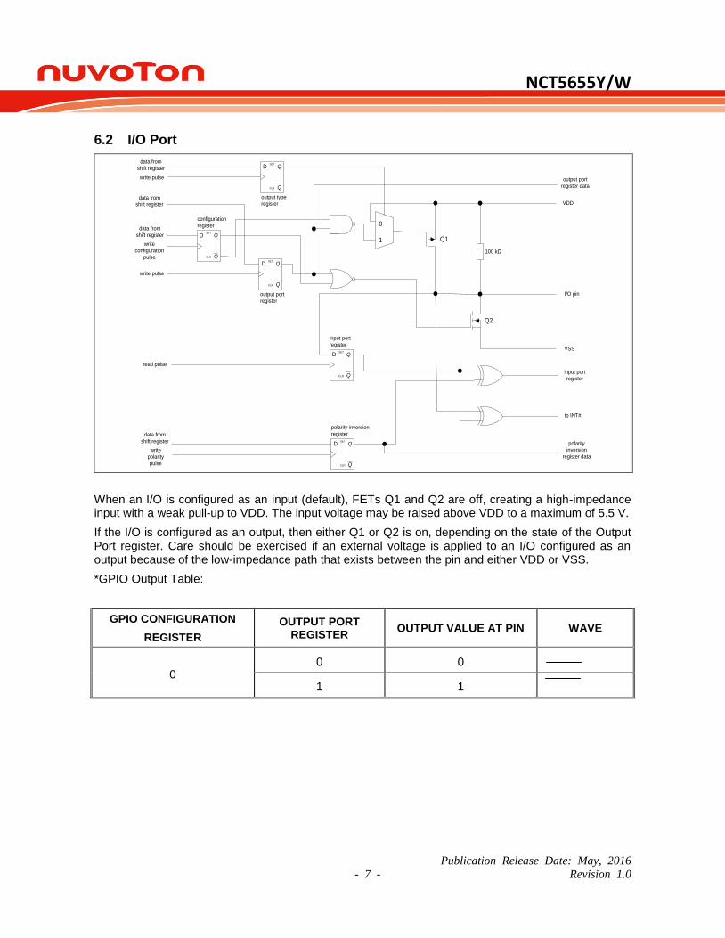
6.2 I/O Port
Q1
Q2
Q
QSET
CLR
D
output port
register
Q
QSET
CLR
D
input port
register
Q
QSET
CLR
D
configuration
register
Q
QSET
CLR
D
polarity inversion
register
100 kΩ
read pulse
data from
shift register
write
configuration
pulse
write pulse
data from
shift register
data from
shift register
write
polarity
pulse
output port
register data
VDD
I/O pin
VSS
input port
register
to INT#
polarity
inversion
register data
0
1
Q
QSET
CLR
D
output type
register
data from
shift register
write pulse
When an I/O is configured as an input (default), FETs Q1 and Q2 are off, creating a high-impedance input with a weak pull-up to VDD. The input voltage may be raised above VDD to a maximum of 5.5 V.
If the I/O is configured as an output, then either Q1 or Q2 is on, depending on the state of the Output Port register. Care should be exercised if an external voltage is applied to an I/O configured as an output because of the low-impedance path that exists between the pin and either VDD or VSS.
*GPIO Output Table:
GPIO CONFIGURATION
REGISTER
OUTPUT PORT REGISTER
OUTPUT VALUE AT PIN WAVE
0 0 0
1 1
NCT5655Y/W
Publication Release Date: May, 2016
- 8 - Revision 1.0
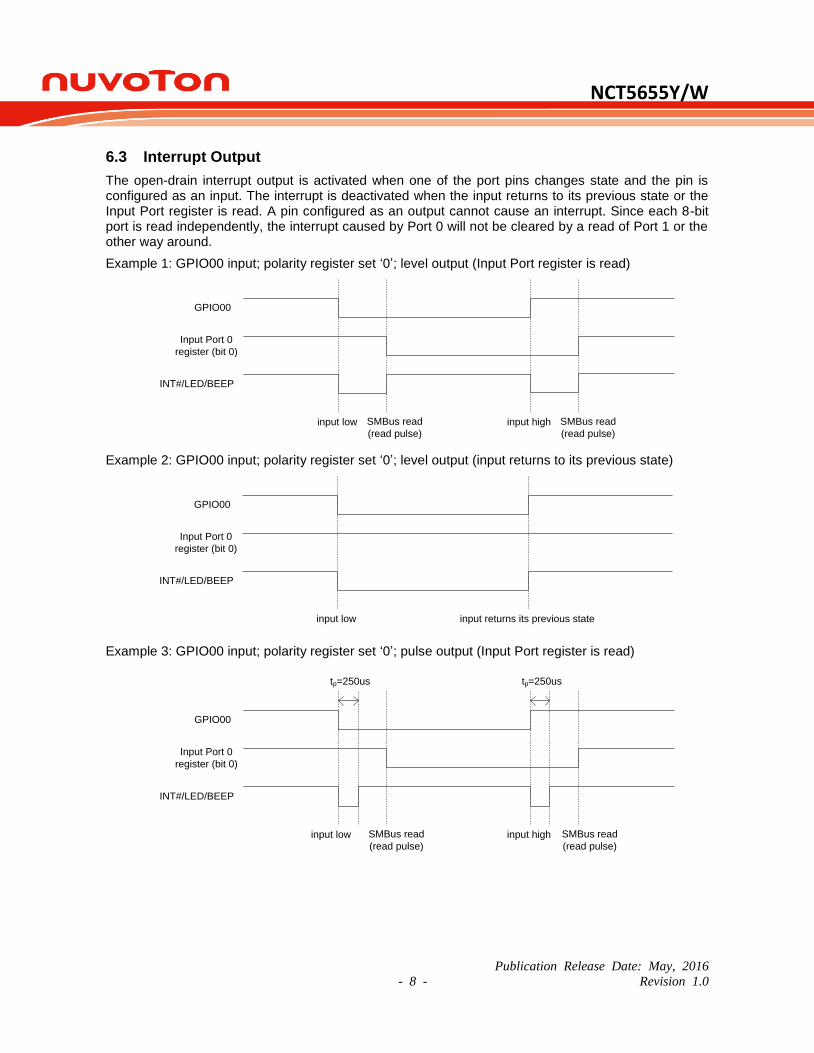
6.3 Interrupt Output
The open-drain interrupt output is activated when one of the port pins changes state and the pin is configured as an input. The interrupt is deactivated when the input returns to its previous state or the Input Port register is read. A pin configured as an output cannot cause an interrupt. Since each 8-bit port is read independently, the interrupt caused by Port 0 will not be cleared by a read of Port 1 or the other way around.
Example 1: GPIO00 input; polarity register set ‘0’; level output (Input Port register is read)
GPIO00
Input Port 0
register (bit 0)
INT#/LED/BEEP
input low input highSMBus read
(read pulse)
SMBus read
(read pulse)
Example 2: GPIO00 input; polarity register set ‘0’; level output (input returns to its previous state)
GPIO00
Input Port 0
register (bit 0)
INT#/LED/BEEP
input low input returns its previous state
Example 3: GPIO00 input; polarity register set ‘0’; pulse output (Input Port register is read)
GPIO00
Input Port 0
register (bit 0)
INT#/LED/BEEP
input low input highSMBus read
(read pulse)
SMBus read
(read pulse)
tp=250us tp=250us

NCT5655Y/W
Publication Release Date: May, 2016
- 9 - Revision 1.0
Example 4: GPIO00 input; polarity register set ‘0’; pulse output (input returns to its previous state)
GPIO00
Input Port 0
register (bit 0)
INT#/LED/BEEP
input low input returns to its previous state
tp=250us
*INT#/LED/BEEP output LED signal during low period when it is configured to LED output.
*INT#/LED/BEEP output BEEP signal during low period when it is configured to BEEP output.
INT# Output Mode Table:
INT OUTPUT MODE POLARITY OUTPUT WAVE
Level 0 0
1 1
Pulse 0 Low Pulse
1 High Pulse
*In level mode, if INT# is activated, it will be de-activated when Input Port register is read or when input returns to its previous state. (Example 1~2)
*In pulse mode, interrupt will be activated again unless Input Port register is read or unless input returns to its previous state and changes again. (Example 3~4)
*The INT# pulse mode output waveform width is 250uS.
* The control register is Register 10h.

NCT5655Y/W
Publication Release Date: May, 2016
- 10 - Revision 1.0
7. REGISTER DESCRIPTION
7.1 Register 00h – GPIO0x Input port register
This register is an input-only port. It reflects the incoming logic levels of the pins, regardless of whether the pin is defined as an input or an output by Register 06h. This register is read only.
BIT 7 6 5 4 3 2 1 0
R/W RO RO RO RO RO RO RO RO
Default X X X X X X X X
*This register reflects the respective GPIO0 pins level. *The default value ‘X’ is determined by the externally applied logic level.
7.2 Register 01h – GPIO1x Input port register
This register is an input-only port. It reflects the incoming logic levels of the pins, regardless of whether the pin is defined as an input or an output by Register 07h. This register is read only.
BIT 7 6 5 4 3 2 1 0
R/W RO RO RO RO RO RO RO RO
Default X X X X X X X X
*This register reflects the respective GPIO1 pins level. *The default value ‘X’ is determined by the externally applied logic level.
7.3 Register 02h – GPIO0x Output port register
This register is an output-only port. It reflects the outgoing logic levels of the pins defined as outputs by Register 06h. Bit values in this register have no effect on pins defined as inputs. In turn, reads from this register reflect the value that is in the flip-flop controlling the output selection, not the actual pin value.
BIT 7 6 5 4 3 2 1 0
R/W RW RW RW RW RW RW RW RW
Default 1 1 1 1 1 1 1 1
7.4 Register 03h – GPIO1x Output port register
This register is an output-only port. It reflects the outgoing logic levels of the pins defined as outputs by Register 07h. Bit values in this register have no effect on pins defined as inputs. In turn, reads from this register reflect the value that is in the flip-flop controlling the output selection, not the actual pin value.
BIT 7 6 5 4 3 2 1 0
R/W RW RW RW RW RW RW RW RW
Default 1 1 1 1 1 1 1 1

NCT5655Y/W
Publication Release Date: May, 2016
- 11 - Revision 1.0
7.5 Register 04h – GPIO0x Polarity Inversion register
This register allows the user to invert the polarity of the Input port register data. If a bit in this register is set (written with ‘1’), the Input port data polarity is inverted. If a bit in this register is cleared (written with ‘0’), the Input port data polarity is retained.
BIT 7 6 5 4 3 2 1 0
R/W RW RW RW RW RW RW RW RW
Default 0 0 0 0 0 0 0 0
7.6 Register 05h – GPIO1x Polarity Inversion register
This register allows the user to invert the polarity of the Input port register data. If a bit in this register is set (written with ‘1’), the Input port data polarity is inverted. If a bit in this register is cleared (written with ‘0’), the Input port data polarity is retained.
BIT 7 6 5 4 3 2 1 0
R/W RW RW RW RW RW RW RW RW
Default 0 0 0 0 0 0 0 0
7.7 Register 06h – GPIO0x Configuration register
This register configures the directions of the I/O pins. If a bit in this register is set (written with ‘1’), the corresponding port pin is enabled as an input with high-impedance output driver. If a bit in this register is cleared (written with ‘0’), the corresponding port pin is enabled as an output. Note that there is a high value resistor tied to VDD at each pin. At reset, the device’s ports are inputs with a pull-up to VDD.
BIT 7 6 5 4 3 2 1 0
R/W RW RW RW RW RW RW RW RW
Default 1 1 1 1 1 1 1 1
*This register configures the respective GPIO0 pins as input mode (‘1’) or output mode (‘0’).
7.8 Register 07h – GPIO1x Configuration register
This register configures the directions of the I/O pins. If a bit in this register is set (written with ‘1’), the corresponding port pin is enabled as an input with high-impedance output driver. If a bit in this register is cleared (written with ‘0’), the corresponding port pin is enabled as an output. Note that there is a high value resistor tied to VDD at each pin. At reset, the device’s ports are inputs with a pull-up to VDD.
BIT 7 6 5 4 3 2 1 0
R/W RW RW RW RW RW RW RW RW
Default 1 1 1 1 1 1 1 1
*This register configures the respective GPIO1 pins as input mode (‘1’) or output mode (‘0’).
NCT5655Y/W
Publication Release Date: May, 2016
- 12 - Revision 1.0
7.9 Register 10h – INT#/LED/BEEP Configuration register
More INT#/LED/BEEP function description is in 6.3 Interrupt Output section.
BIT 7 6 5 4 3 2 1 0
R/W RW RW RW RW RW RW RW RW
Default 0 0 0 0 0 0 0 0
Bit1-Bit0: INT# output select register = 11, Reserved = 10, BEEP output = 01, LED output = 00, INT# output Bit2: INT# output type register = 1, Pulse mode = 0, Level mode Bit3: INT# polarity select register = 1, Inverted = 0, Non-inverted Bit5-4: LED configuration register
=11, LED frequency = 2 Hz; duty-cycle 50% =10, LED frequency = 1 Hz; duty-cycle 50% =01, LED frequency = 0.5 Hz; duty-cycle 50% =00, LED function is disabled
Bit7-6: BEEP configuration register =11, BEEP frequency = 4K Hz; tone = 250 Hz =10, BEEP frequency = 2K Hz; tone = 10 Hz =01, BEEP frequency = 1K Hz / 500 Hz; tone= 1 Hz =00, BEEP function is disabled
7.10 Register 12h – GPIO0x Output type register
This register configures the output type of the GPIO0 I/O pins. If a bit in this register is set (written with ‘1’), the corresponding output port is enabled as a push-pull output driver. If a bit in this register is cleared (written with ‘0’), the corresponding output port is enabled as an open-drain output driver. Note that there is a high value resistor tied to VDD at each pin.
BIT 7 6 5 4 3 2 1 0
R/W RW RW RW RW RW RW RW RW
Default 1 1 1 1 1 1 1 1
*This register configures the respective GPIO0 pins as push-pull mode (‘1’) or open-drain mode (‘0’).

NCT5655Y/W
Publication Release Date: May, 2016
- 13 - Revision 1.0
7.11 Register 13h – GPIO1x Output type register
This register configures the output type of the GPIO1 I/O pins. If a bit in this register is set (written with ‘1’), the corresponding output port is enabled as a push-pull output driver. If a bit in this register is cleared (written with ‘0’), the corresponding output port is enabled as an open-drain output driver. Note that there is a high value resistor tied to VDD at each pin.
BIT 7 6 5 4 3 2 1 0
R/W RW RW RW RW RW RW RW RW
Default 1 1 1 1 1 1 1 1
*This register configures the respective GPIO1 pins as push-pull mode (‘1’) or open-drain mode (‘0’).
7.12 Register 14h – LED Configuration register
This register configures the output signal of the GPIO10/LED0~GPIO13/LED3 I/O pins. When output LED signal, the pin must define as an output by Register 07h. For GPIO function use, the corresponding register must set to “00”.
BIT 7 6 5 4 3 2 1 0
R/W RW RW RW RW RW RW RW RW
Default 0 0 0 0 0 0 0 0
Bit1-Bit0: GPIO10/LED0 configuration register =11, LED frequency = 2 Hz; duty-cycle 50% =10, LED frequency = 1 Hz; duty-cycle 50% =01, LED frequency = 0.5 Hz; duty-cycle 50% =00, LED function is disabled
Bit3-Bit2: GPIO11/LED1 configuration register =11, LED frequency = 2 Hz; duty-cycle 50% =10, LED frequency = 1 Hz; duty-cycle 50% =01, LED frequency = 0.5 Hz; duty-cycle 50% =00, LED function is disabled
Bit5-Bit4: GPIO12/LED2 configuration register =11, LED frequency = 2 Hz; duty-cycle 50% =10, LED frequency = 1 Hz; duty-cycle 50% =01, LED frequency = 0.5 Hz; duty-cycle 50% =00, LED function is disabled
Bit7-Bit6: GPIO13/LED3 configuration register =11, LED frequency = 2 Hz; duty-cycle 50% =10, LED frequency = 1 Hz; duty-cycle 50% =01, LED frequency = 0.5 Hz; duty-cycle 50% =00, LED function is disabled

NCT5655Y/W
Publication Release Date: May, 2016
- 14 - Revision 1.0
7.13 Register 15h – BEEP Configuration register
This register configures the output signal of the GPIO14/BEEP I/O pins. When output BEEP signal, the pin must define as an output by Register 07h. For GPIO function use, the corresponding register must set to “00”.
BIT 7 6 5 4 3 2 1 0
R/W RO RO RO RO RO RO RW RW
Default 0 0 0 0 0 0 0 0
Bit1-0: GPIO14/BEEP configuration register =11, BEEP frequency = 4K Hz; tone = 250 Hz =10, BEEP frequency = 2K Hz; tone = 10 Hz =01, BEEP frequency = 1K Hz / 500 Hz; tone= 1 Hz =00, BEEP function is disabled
7.14 Register 18h – Register ON/OFF Configuration register
This register configures the register 10h~1Fh on/off for this chip.
BIT 7 6 5 4 3 2 1 0
R/W RO RO RO RO RO RO RO RW
Default 0 0 0 0 0 0 0 1
Bit0: Register 10h~1Fh ON/OFF configuration register =1, registers 10h~1Fh will be off. =0, registers 10h~1Fh will be on.
Bit7-1: Reserved.
7.15 Register 1Dh – Chip ID high byte register
This register indicates the high byte of the Chip ID.
BIT 7 6 5 4 3 2 1 0
R/W RO RO RO RO RO RO RO RO
Default 1 1 0 1 0 0 0 1
7.16 Register 1Eh – Chip ID low byte register
This register indicates the low byte of the Chip ID.
BIT 7 6 5 4 3 2 1 0
R/W RO RO RO RO RO RO RO RO
Default 0 1 0 0 X X X X
Bit3-0: XXXX=0000~1111

NCT5655Y/W
Publication Release Date: May, 2016
- 15 - Revision 1.0
8. DC AND AC SPECIFICATION
8.1 Absolute Maximum Ratings
PARAMETER RATING UNIT
Power Supply Voltage 2.3 to 5.5 V
Input Voltage 2.3 to 5.5 V
Operating Temperature -40 to +85 C
Note: Exposure to conditions beyond those listed under Absolute Maximum Ratings may adversely affect the life
and reliability of the device.
8.2 DC Characteristics
DC characteristics at VDD=2.3V to 5.5V; VSS=0V; Tamb=-40℃ to +85℃; unless otherwise specified.
Symbol Parameter Conditions Min. Typ. Max. Unit
Supply
VDD Supply Voltage 2.3 - 5.5 V
IDD Supply Current Operating mode; VDD=5.5V; no load; fSCL=100KHz
- 135 200 uA
Istb Standby Current
Standby mode; VDD=5.5V;
no load; VI=VSS; fSCL=0KHz;
I/O=inputs
Standby mode; VDD=5.5V;
no load; VI=VDD; fSCL=0KHz;
I/O=inputs
-
-
1.1
0.25
1.5
1
mA
uA
VPOR Power-on reset voltage No load; VI=VDD or VSS - 1.5 1.65 V
Input SCL; input/output SDA
VIL LOW-level input voltage -0.5 - +0.3VDD V
VIH HIGH-level input voltage 0.7VDD - 5.5 V
IOL LOW-level output current VOL=0.4V 3 - - mA
IL leakage current VI=VDD or VSS -1 - +1 uA
Ci input capacitance VI=VSS - 6 10 pF
I/Os
VIL LOW-level input voltage -0.5 - +0.3VDD V

NCT5655Y/W
Publication Release Date: May, 2016
- 16 - Revision 1.0
Symbol Parameter Conditions Min. Typ. Max. Unit
VIH HIGH-level input voltage 0.7VDD - 5.5 V
IOL LOW-level output current VDD=2.3V to 5.5V; VOL=0.5V
VDD=2.3V to 5.5V; VOL=0.7V
8
10
(8 to 20)
(10 to 24)
-
-
mA
mA
VOH HIGH-level output voltage
IOH=-8mA; VDD=2.3V
IOH=-10mA; VDD=2.3V
IOH=-8mA; VDD=3.0V
IOH=-10mA; VDD=3.0V
IOH=-8mA; VDD=4.75V
IOH=-10mA; VDD=4.75V
1.8
1.7
2.6
2.5
4.1
4.0
-
-
-
-
-
-
-
-
-
-
-
-
V
V
V
V
V
V
ILIH HIGH-level input leakage current
VDD=5.5V; VI=VDD - - 1 uA
ILIL LOW-level input leakage current
VDD=5.5V; VI=VDD - - -100 uA
Ci input capacitance - 3.7 5 pF
Co output capacitance - 3.7 5 pF
Interrupt INT_N
IOL LOW-level output current VOL=0.4V 3 - - mA
Select Inputs A0, A1, A2
VIL LOW-level input voltage -0.5 - +0.3VDD V
VIH HIGH-level input voltage 0.7VDD - 5.5 V
ILI input leakage current pin at VDD or VSS -1 - +1 uA
NCT5655Y/W
Publication Release Date: May, 2016
- 17 - Revision 1.0
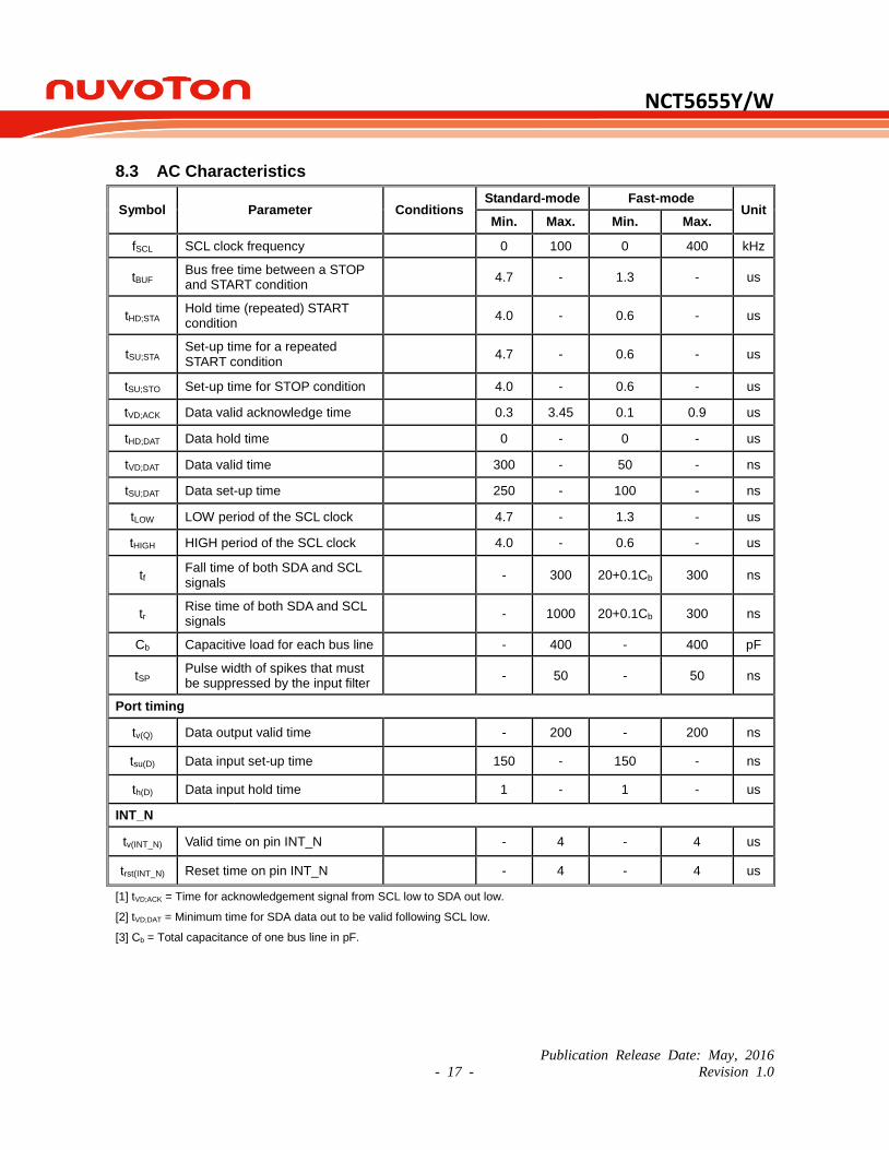
8.3 AC Characteristics
Symbol Parameter Conditions Standard-mode Fast-mode
Unit Min. Max. Min. Max.
fSCL SCL clock frequency 0 100 0 400 kHz
tBUF Bus free time between a STOP and START condition
4.7 - 1.3 - us
tHD;STA Hold time (repeated) START condition
4.0 - 0.6 - us
tSU;STA Set-up time for a repeated START condition
4.7 - 0.6 - us
tSU;STO Set-up time for STOP condition 4.0 - 0.6 - us
tVD;ACK Data valid acknowledge time 0.3 3.45 0.1 0.9 us
tHD;DAT Data hold time 0 - 0 - us
tVD;DAT Data valid time 300 - 50 - ns
tSU;DAT Data set-up time 250 - 100 - ns
tLOW LOW period of the SCL clock 4.7 - 1.3 - us
tHIGH HIGH period of the SCL clock 4.0 - 0.6 - us
tf Fall time of both SDA and SCL signals
- 300 20+0.1Cb 300 ns
tr Rise time of both SDA and SCL signals
- 1000 20+0.1Cb 300 ns
Cb Capacitive load for each bus line - 400 - 400 pF
tSP Pulse width of spikes that must be suppressed by the input filter
- 50 - 50 ns
Port timing
tv(Q) Data output valid time - 200 - 200 ns
tsu(D) Data input set-up time 150 - 150 - ns
th(D) Data input hold time 1 - 1 - us
INT_N
tv(INT_N) Valid time on pin INT_N - 4 - 4 us
trst(INT_N) Reset time on pin INT_N - 4 - 4 us
[1] tVD;ACK = Time for acknowledgement signal from SCL low to SDA out low.
[2] tVD;DAT = Minimum time for SDA data out to be valid following SCL low.
[3] Cb = Total capacitance of one bus line in pF.

NCT5655Y/W
Publication Release Date: May, 2016
- 18 - Revision 1.0
Definition of timing on the I2C-bus/SMBus

NCT5655Y/W
Publication Release Date: May, 2016
- 19 - Revision 1.0
9. ORDERING INFORMATION
PART NUMBER PACKAGE TYPE REMARK
NCT5655Y QFN24 Green Package (Halogen-free)
NCT5655W TSSOP24 Green Package (Halogen-free)
10. TOP MARKING SPECIFICATION
NCT5655Y
618
GA E41700
03-xx
NCT5655W 618GASA
1st line: Part number NCT5655Y
2nd
~ 4th line: Tracking code
618: Packages assembled in Year 2016, week 18
G: Assembly house ID
A: IC version
E4170003-xx: Lot number
1st line: Nuvoton Logo
2nd
line: Part number: NCT5655W
3rd
line: Tracking code: 618 GA SA
618: Packages assembled in Year 2015, week 18
G: Assembly house ID
A: IC version
SA: Internal use code

NCT5655Y/W
Publication Release Date: May, 2016
- 20 - Revision 1.0
11. PACKAGE DIMENSION OUTLINE
11.1 QFN 24L 4x4mm2, Thickness: 0.8mm, Pitch:0.50mm

NCT5655Y/W
Publication Release Date: May, 2016
- 21 - Revision 1.0
11.2 TSSOP 24L 4.4x7.8 mm2

NCT5655Y/W
Publication Release Date: May, 2016
- 22 - Revision 1.0
Important Notice
Nuvoton Products are neither intended nor warranted for usage in systems or equipment, any malfunction or failure of which may cause loss of human life, bodily injury or severe property damage. Such applications are deemed, “Insecure Usage”.
Insecure usage includes, but is not limited to: equipment for surgical implementation, atomic energy control instruments, airplane or spaceship instruments, the control or operation of dynamic, brake or safety systems designed for vehicular use, traffic signal instruments, all types of safety devices, and other applications intended to support or sustain life.
All Insecure Usage shall be made at customer’s risk, and in the event that third parties lay claims to Nuvoton as a result of customer’s Insecure Usage, customer shall indemnify the damages and liabilities thus incurred by Nuvoton.
Related Documents


![[MSP430] GPIO](https://static.cupdf.com/doc/110x72/55cf9df0550346d033aff200/msp430-gpio.jpg)


