Numerical Simulation of a Balanced Optical Microwave Phase Detector (BOMPD) in CppSim Ognjen Markovi´ c, University of Cambridge, UK September 10, 2014 Abstract A report on a project done at the DESY summer school during the summer of 2014 is given. The simulation of a Balanced Optical Microwave Phase Detector (BOM-PD) was done in a custom system simulation package CppSim. A simple but robust model was made allowing for qualitative simulation of BOMPD properties and noise performance with noise sources coming from the VCO, photo-detection proccess and from the optical input. The model is easily extensible so a precise simulation of current experimental results is possible. 1

Welcome message from author
This document is posted to help you gain knowledge. Please leave a comment to let me know what you think about it! Share it to your friends and learn new things together.
Transcript

Numerical Simulation of a Balanced Optical MicrowavePhase Detector (BOMPD) in CppSim
Ognjen Markovic, University of Cambridge, UK
September 10, 2014
Abstract
A report on a project done at the DESY summer school during the summer of 2014 is given.The simulation of a Balanced Optical Microwave Phase Detector (BOM-PD) was done in acustom system simulation package CppSim. A simple but robust model was made allowingfor qualitative simulation of BOMPD properties and noise performance with noise sourcescoming from the VCO, photo-detection proccess and from the optical input. The model iseasily extensible so a precise simulation of current experimental results is possible.
1

Contents
1 Introduction 2
2 Microwave-signal synthesis from mode-locked lasers 32.1 Methods of microwave-signal synthesis from mode-locked lasers . . . . . . . . . . 3
3 BOMPD 43.1 Description of the BOMPD . . . . . . . . . . . . . . . . . . . . . . . . . . . . . 43.2 Past experimental results . . . . . . . . . . . . . . . . . . . . . . . . . . . . . . . 5
4 Method 64.1 CppSim . . . . . . . . . . . . . . . . . . . . . . . . . . . . . . . . . . . . . . . . 64.2 Implementation of the BOMPD . . . . . . . . . . . . . . . . . . . . . . . . . . . 64.3 Implementation of noise in the BOMPD . . . . . . . . . . . . . . . . . . . . . . 7
5 Results 85.1 Ideal model and convergence . . . . . . . . . . . . . . . . . . . . . . . . . . . . . 85.2 Inclusion of noise . . . . . . . . . . . . . . . . . . . . . . . . . . . . . . . . . . . 10
6 Conclusion 12
1 Introduction
In this report I describe the project I did during the DESY student summer programme inHamburg. The project was concerned with a simulation of a Balanced Optical Microwave PhaseDetector (BOMPD) used for low noise synchronization of a tunable microwave signal source toa mode-locked loser.
Ultra-stable microwave signals are needed in next generation X-ray FELs, such is the EuropeanXFEL being built in DESY. These large-scale X-ray FEL facilities require extremely stringenttiming precision and accuracy on large scales. This is done by using an ultra-low-jitter mode-locked laser as a master oscillator and syncrhonizing it with different sections of the systemwith timing-stabilized links. Figure 1. shows the schematic layot of the timing syncrhonization
Figure 1: A schematic of a large-scale Free Electron Laser (FEL) system. The master oscillatormode-locked laser is used as a timing reference for the different parts of the system.Optical-to-microwave synchronization is used to produce a highly stable RF signalused to drive the electron beams through accelerator sections.
2

system that is be used for large-scale X-ray FELs. The starting point of the system is the mode-locked laser locked to an optical or a microwave standard which serves as the optical masteroscillator of the system. Different lasers used in the FEL can be synchronized by optical-to-optical synchronization with the master laser. Optical-to-microwave stabilization is needed tosyncrhonize the RF sources which drive the accelerator sections. The electron-beam dynamicsis controlled by the microwave fields in the accelerator cavities and therefore a highly stablemicrowave signal, tightly synchronized between different accelerator sections is needed.
In Section 2. of this report I present an introduction to Microwave-signal synthesis frommode-locked lasers. In Section 3. I describe the operation of the Balanced Optical MicrowavePhase Detector (BOMPD). In Section 4. I present methods and tools used to write an accuratesimulation of a BOMPD. In Section 5. I describe the results obtained using this simulation andfinally in Section 6. a conclusion on the project is given.
2 Microwave-signal synthesis from mode-locked lasers
Ultra-short optical pulse generation from mode-locked lasers has been long used for studies ofphysical phenomena on picosecond and femtosecond time scales. In the frequency domain, theoptical pulse train from a mode-locked laser looks like a series of equaly spaced lines, whichis called a frequency comb. The distance between these lines is set by the repetition rate ofthe pulses in the time domain, frep. Ultra-low timing jitter of optical wave trains can be usedfor the high-precision generation, distribution, measurement, and synhronization of optical andmicrowave signals. Optical pulse trains generated from standard, passively mode-locked Er-fiberlasers can easily achieve sub-10-fs and sub-fs timing jitter [1], while TiSa lasers can achieve evenlower jitters.
2.1 Methods of microwave-signal synthesis from mode-locked lasers
Transfer of timing stability from the optical domain to the electronic domain is a challengingtask [1]. The simplest way to generate a microwave signal from an optical pulse is direct pho-todetection using a photo diode which output is filtered to a desired frequency. This methodsuffers from excess phase noise (as given in [2]), which originates from aplitude-to-phase conver-sion in the photodetectors and microwave mixers. Then power drifts of the optical pulse trainconverts into excess timing jitter and drifts, and therefore a long term stability of the signal isdegraded. Amplitude-to-phase conversion factor of photodiodes measured in [2] ranges from 1to 10ps/mW, depending on the photodiode used. For and Er-doped fiber liser with 0.03%rms
relative intensity noise this lead to 5-fs excess jitter when 10 mW of power is applied to thephotodiode. But it is possible to limit the short-term jitter to 1-fs levels by a supression ofexcess noise sources. Still long-term jitter is large and for example measured to be 56ms in 100sas shown in [2].
To by-pass the amplitude-to-phase conversion an optoelectronic phase-locked loop (PLL) canbe used synchronizing the optical pulse train with a high-quality voltage-controlled oscillator(VCO). The key issue here becomes a development of a drift-free, low-jitter phase detector toextract the phase difference between the input optical wave train and the output microwavesignal in the optical domain. Thus a timing error information is obtained in the optical domainand then fed into a VCO by a photo detection proccess which avoids the timing/phase drift ofthe photodetection and amplification stages. The schematic representation of a Opto-electronicPhase-Locked Loop (PLL) is given in Figure 2.
One of the methods used is the microwave synchronization using balanced intensity detector.In this case the phase error is converted into intensity imbalance between two optical pulses
3

Figure 2: A schematic representation of an Opto-electronic Phase-Locked Loop.
from two differentially modulated intensity modulators and this information is used to close theloop. This was first described in [3].
3 BOMPD
The synchronization of microwave signals with optical pulse trains based on the balanced-intensity detection provides a very simple interface between the optical and electronic domainsbut it is difficult to scale the noise performance because of the limited optical power applicableto the photodiode and the drift in beam combining and splitting [1]. The Balanced OpticalMicrowave-Phase Detector (BOMPD) avoids these problems by using a differentially biasedSagnac fiber loop first described and implemented in [4].
3.1 Description of the BOMPD
A schematic of a BOMPD is given in Figure 3. Inputs to the BOM-PD are the optical pulsetrain at a frequency fr and the microwave signal with a frequency f0 generated by a VCO. In thelocked state the frequency of the VCO is locked to a comb-line in the frequency spectrum of themode locked laser such that f0 = Nfr where N is an odd integer. As a black-box the BOMPDproduces a voltage signal ∆V proportional to the phase difference θe between the optical pulsetrain and the microwave signal when the phase difference is small, ∆V = KPD · θe. This errorsignal is fed into a feedback Proportional-Integral controler (PI controler) which drives the VCOinput and this closes the PLL operation.
The Sagnac-loop fiber integral in the BOMPD consits of a 50:50 coupler which splits the inputoptical signal and produces two counter-propagating pulses, fiber loop, and an unidirectionalphase modulator which phase-shifts only clockwise propagating pulse. These pulses interfere onthe output of the Sagnac loop, and the output optical power is given as Pout = Pin sin2(∆φ/2)([5]), where ∆φ is the net phase shift between two propagating pulses and is proportional to thevoltage applied to the phase modulator. When no RF signal is applied to the phase modulator,the output optical power is 0 i.e. the pulses interfere destructively.
A reference signal is isolated from the input optical pulse train, by photo-detection and filteringthe signal at the odd-harmonic of the optical pulse train (Nfr = (2n + 1)fr). This signal isfrequency divided by a factor of two and and then applied to the phase modulator. The clockwisesub-pulse will obtain alternating phase shifts because it is aligned with maxima/minima in thevoltage signal alteratingly, but the output optical power will still be zero as evident from theSagnac loop transmission function (Figure 4.).
Next step is to apply a sum of the reference signal and the VCO outpur to the phase modulator.Then the output optical pulse train is modulated by a half-repetition frequency fr/2 becausethe phase modulation by the VCO signal will have the same polarity on adjecent pulses whichmoves the biasing points to left or right in the Sagnac loop transmission function (Figure 4.)depending on whether θe is smaller or larger than zero. When phase error is small then themodulation depth of the output optical signal is proportional to θe as derived in [5]. In this stepthe phase/time mismatch was converted to amplitude modulation in the optical domain, and
4

Figure 3: Schematic representation of a Balanced Optical Microwave Phase detector.
Figure 4: Sampling of the input optical signal by a Sagnac-loob fiber. On the top of each picturea graph of Sagnac-loop transmission function Pout = Pin sin2(∆φ/2) is shown. a)no applied signal to the phase modulator and the output optical power is zero. b)reference signal of frequency (n+ 1/2)fr is applied producing no modulation c) addedVCO signal to reference produces amplitude modulation proportional to the phaseerror.
therefore it is not susceptible to the amplitude-to-phase conversion in the photodetection process.To get the error signal in the electronic domain to drive the VCO, the photodetected outputfrom the Sagnac loop is first band filtered to the reference frequency and then downconvertedby mixing it with the reference signal and then passing it through a low-pass filter. This erroris input to the PI controler which drives the VCO, and this completes the PLL operation.
3.2 Past experimental results
As first reported in [4] and in [5], the BOMPD shows excelent noise performance, with a shortterm jitter of 12.8 fs and a long-time jitter of 48fs with measurement times up to 4 hours. Laterresults as reported in [6] were that short-term jitter is 4.4 fs integrated from 1 Hz to 1 MHz,which is higher than the best direct photodetection result. On the other hand the long-termmeasurement shows a sub 10 fs jitter which corresponds to a relative stability of 10−19. Thenewest results, [7], bring these results to less than 2 fs RMS jitter in short term and less than 1fs RMS jitter in the long term. As shown in [5] the fundamental noise floor to the BOMPD is
5

limited by the shot noise in the photodiodes but in the real experiments this is usually determinedby other noise sources and non-linearities such as those in amplifiers.
4 Method
The primary motivation for the simulation of the BOMPD was to make a workable model whichcould be used in future experiments as a benchamrk on what could be achieved in the experiment.The simulation package used is CppSim, a free package for system simulation written by MichaelH. Perrott. It is particulary suited for simulation of PLLs using special techniques for accuratesimulations of PLLs described in [9]. The underlying code is written in C++ allowing for fastexecution times. CppSim provides a large library of C++ classes useful for system simulationand signal analysis. Several classes included provide easy analysis of simulated signals, elaboratecontrol over input and output parameters, sampling of the output signals and edge detection forjitter calculations.
4.1 CppSim
CppSim package includes a GUI program Sue2, a signal viewing program CppSimView and a setof C++ classes which describe the basic elements that can be used in CppSim simulations. TheSue2 program is a CAD-like program for graphicaly constructing a system using pre-defined oruser-defined blocks. The schematic made is then converted to a ”netlist” format, which describesthe included blocks in a hierarchical manner. Then on running the simulation CppSim convertsthis file into C++ code using the definitions of primitives given by a library of C++ classes.Common system blocks are included like VCOs, amplifiers and filters which enable easy buildingof more complex objects. The internal approach in CppSim to simulating systems is to use nodalanalysis with output at a node depending on the input and the internal state of the node. Ateach simulation time-step the states of nodes are calculated sequentaly.
4.2 Implementation of the BOMPD
The modules used in the BOMPD simulation were mostly already implemented in the CppSim,with some modules implemented manually. First step was to make a perfect model of a BOMPDwithout any noise to prove that it is possible to simulate the BOMPD in CppSim. Next im-perfections were added such as the VCO noise, photo-diode noise and optical source noise. Themain modules included were:
• Optical source element is producing a train of single point pulses at the repetition frequencyfr. It was taken from the example library OpticalPLL Example included with CppSim.The power of the optical source is a parameter of the element. It uses the signal sourceelement which can generate sine, square or pulse outputs. It also allows for simulatingnoise by inputing the phase imput into the ”phase” input of the element.
• Sagnac loop was implemented as a simple element with two inputs; optical one which ismodulated through a perfect mixer by the sin2 of the half of the electrical input, whichreplicates the transmission function of the Sagnac loop.
• The band-pass filter and low-pass filter were already implemented in CppSim.
• VCO element used was one already implemented in CppSim, both noisless and noisyversion. The photodiodes were simple gain elements in the perfect model.
6

• PI controler is implemented as an element adding the integrated and proportional signals.The gain parameter is Kp or the proportional parameter, and the integrator parameter isKi or the integration parameter of the PI controler.
The view of the Sue2 modeling program and the ideal model of the BOMPD is presented in Fig.5.
Figure 5: The view of the Sue2 modeling program belonging to the CppSim package. In thecentral view is a perfect model of a Balanced Optical Microwave-Phase Detector(BOMPD) consisting of multiple elements representing optical and electrical com-ponents of a real BOMPD.
Main parts of the model are the reference arm, the Sagnac loop arm and then the phase erroroutput of the BOMPD which is input into the PI controler and then into the VCO. In theexperimental implementation of a BOMPD the reference arm uses a digital frequency divider ona filtered input optical signal. In our simplified model this was deemed unnessecery to implement,so a reference was provided by a VCO at the desired reference frequency. It was made sure thatsignals in the simulation have a sensical physical units. The optical signals were adjusted bythe optical source power. The electrical signals output from the main VCO and the referenceVCO were adjusted by a power amp element in units of dBm. The conversion coefficient ofthe photo-diode was given in units of mV/mW of input optical power. Band-pass and low-passfilters transfer function were unit-less.
4.3 Implementation of noise in the BOMPD
CppSim provides an implementation of classes and elements which provide random sequenceswith white and 1/f noise spectral power densities. The parameters specified in the white noise
7

element are offset frequency foff and the noise at the offset frequency, noff in dBc/Hz. Theoutput of the is noise varation multiplied by a random Gaussian variable with a mean of 0and a variance of 1. The 1/f noise is implemented in the class OneOverfPlusWhiteNoise [10].It produces a random Gaussian sequence that includes white noise and 1/f noise in the lowfrequencies. The 1/f noise is obtained by filtering the white noise with 6 pole-zero pairs eachseparated 7.5 decades apart. Corner frequency fcorner defines the frequency at which the powerof the white noise component is the same as the power of the 1/f noise.
The noise of the Optical Source element is provided by a twenty db rolloff noise elementimplemented in the OpticalPLL Example library, which gives out the integrated phase noise forthe input phase of the singal source element. The noise of the photo diode was implemented byadding the white noise signal to the output of the photo-diode.
5 Results
Careful calibration of all important parameters in the system was needed to obtain the lockingbetween the optical source and the VCO. In both [4], [5] a 44.26 MHz Er-doped fiber laser wasused, while in later works ([6] and [7]) a higher pulse repetition frequency laser was used of200MHz. In all works a VCO of center frequency of about 10GHz was used. Firstly for theproof of concept optical repetition frequency of 50MHz and the VCO of central frequency ofabout 10GHz were used in the simulation. Following [9], a time step Ts was such that there werefrom 50 to 200 simulation points in one VCO period which is the highest frequency present inthe system. The time step was also set such that 1/Ts was a large even integer of the repetitionfrequency and so that a pulse exactly coincides with a time simulation point. Even in this casea floating point error was observed so phase of the optical signal drifted from its expected valueduring simulation which produced a pulse ”spreading” to two simulation points. The code ofSigGen class was manually changed to account for that error so the intensity from the opticalsource is nevertheless same. In all cases of simulation a trade-off between the length of simulationand the size of the output had to be made. For checking convergence and short-time simulations,number of simulation points nstep was from 5e6 to 1e7 points. In the case for checking long termconvergence, a longer simulation times were needed, up to 1e10 points which took up to 6 hourson an Intel i5 machine.
5.1 Ideal model and convergence
The calibration process for parameters usually started with checking signal levels in all parts ofthe BOMPD. The power of signals input to the mixer was made to be approximately the same.The electrical input to the Sagnac loop was checked such that peak-to-peak values don’t exceedπ/2 (if the signal level was larger then π then the BOMPD could jump to a next minimum inthe transmission function degrading the stability) and also that VCO output and reference armsignals have the same power. It was also made sure that the peaks of the reference signal werealigned with optical pulses which meant delaying the reference signal by one simulation point.Before mixing the reference signal was delayed by a π/2 phase, using a delay element with delayof 1/(4freferenceTs) + 1. The locking frequency at first was taken to be the 201st harmonic of theoptical pulse train so then freference = 100.5fr. Then the bandwidth and gain of the low passwere adjusted such that high-frequency oscilltions are low. Finally the PI controler parameterswere adjusted such that settling time and stability of the BOMPD output are on a desired level.
In Figure 6., a graph of the input to the VCO is given showing settling behaviour of theBOMPD. VCO central frequency was exactly set to the locking frequency so the VCO inputsettles to oscillattion around the zero point. If we zoom in to the settled region we see that theinput to the VCO oscillates with reference frequency, in this case 201fr = 10.05GHz, which is
8

0 0.2 0.4 0.6 0.8 1 1.2 1.4 1.6
x 10−4
−1
−0.5
0
0.5
1
1.5
2x 10
−3
Time [s]
VC
O In
put [
V]
Settling of the BOMPD in the time domain in the perfect case
Figure 6: The input to the Voltage-Controlled Oscilaltor in the BOMPD. The settling behaviourcan clearly be seen, and in the steady state it settles to zero because the VCO frequency,fvco = 10.05GHz was exactly set to be at a reference frequency.
due to the fact that in the perfect model low-pass filter attenuates high frequency signal butdoes not remove it. To check how the BOMPD locks the VCO signal to the input signal wecan plot a graph of phase difference between the optical pulse input and the VCO output. Theplot of phase difference or relative jitter between the optical input and VCO output is shown inFigure 7.
0 1 2 3 4 5 6 7 8 9 10
x 104
−0.7
−0.6
−0.5
−0.4
−0.3
−0.2
−0.1
0
VCO rising edge number
Inst
anta
neou
s Ji
tter
(U.I.
)
Instantaneous Jitter of a VCO in the BOMPD
Figure 7: Instantaneous jitter between the input optical pulse and the output of a VCO. In thesteady state jitter drifts by a small amount.
The locking is good, but not perfect as a drift of relative jitter can be seen over long times.The source of this error is not evident but it is suspected that it comes from a floating-pointerror present in the simulation, more specifically when the simulation calculates the phase of theoptical source and the VCO there could be a relative drift because another ”reference” VCO isused to calculate the relative jitter.
A small table of parameters used in the simulation for obtaining convergence is given in aTable 1. for a reference for future users of this BOMPD simulation.
9

Table 1: Values of parameters used in the simulation of the BOMPD for obtaining convergence.
Ts Ref. frequency fr Optical power LPF fb PI controler Ki
1/(10e10) 5.025e9 1W 1e6 - 25e6 2e6-1e71/5e10 5.25e8 1W 25e6 2.5e51/5e10 5.25e8 1mW 25e6 1e5 - 2e6
5.2 Inclusion of noise
Firstly the noise in the VCO is included by including the VCO element with 1/f noise alreadypresent in the CppSim. The VCO (reference) frequency was reduced to 1.05GHz so that largertime steps could be used in the simulation and thus longer simulation times enabling examinationof the noise performance in low frequency regions. The noise level of the VCO thatt was used forthe presentation of results was 1/f noise with offset frequency foff = 1e6 and the noise level atfoff was -125dBc/Hz. In Figure 8. the settling of the BOMPD in time domain is shown. Thisgraph is very similar to Figure 6. but in the steady state region we observe random fluctuationsaround the settling point which is in this case again around zero. Jitter plot would show asimilar trend as one shown in Figure 7. but with some random fluctuations around the steadypoint. To consider the effectivness and performance of the BOMPD the best thing to do is to
0 0.2 0.4 0.6 0.8 1 1.2 1.4 1.6
x 10−4
−1
−0.5
0
0.5
1
1.5
2x 10
−3
Time [s]
VC
O in
put [
V]
Settling of the BOMPD in the time domain with included noise
Figure 8: The input to the VCO in the BOMPD when the VCO is noisy. The settling behaviourcan clearly be seen, and in the steady state it settles to zero because the VCO frequencywas exactly set to be at a reference frequency.
plot the phase noise in frequency domain of a free-running VCO and of a VCO connected witha BOMPD in-loop. In figure 9, it is clearly seen that BOMPD reduces the phase-noise in thelower frequencies, in this case around 1e5Hz which is the effective bandwidth of the BOMPD inthis case. From these phase-noise measurements integrated timing jitter can be calculated, in arange of frequencies. This was done by integrating the phase noise spectral density from a certainfrequency and then converting the result into timing jitter by scaling it with the VCO frequency.The result of this calculation is shown in Figure 10, where the intgration was done from 10MHz
10
102
103
104
105
106
107
−180
−160
−140
−120
−100
−80
−60
−40
−20
Frequency Offset from Carrier (Hz)
Pha
se n
oise
(dB
c/H
z)
In loop phase noise of the BOMPDPhase noise of the free running VCO, f
off=1e6 n
foff
=−125dBc/Hz
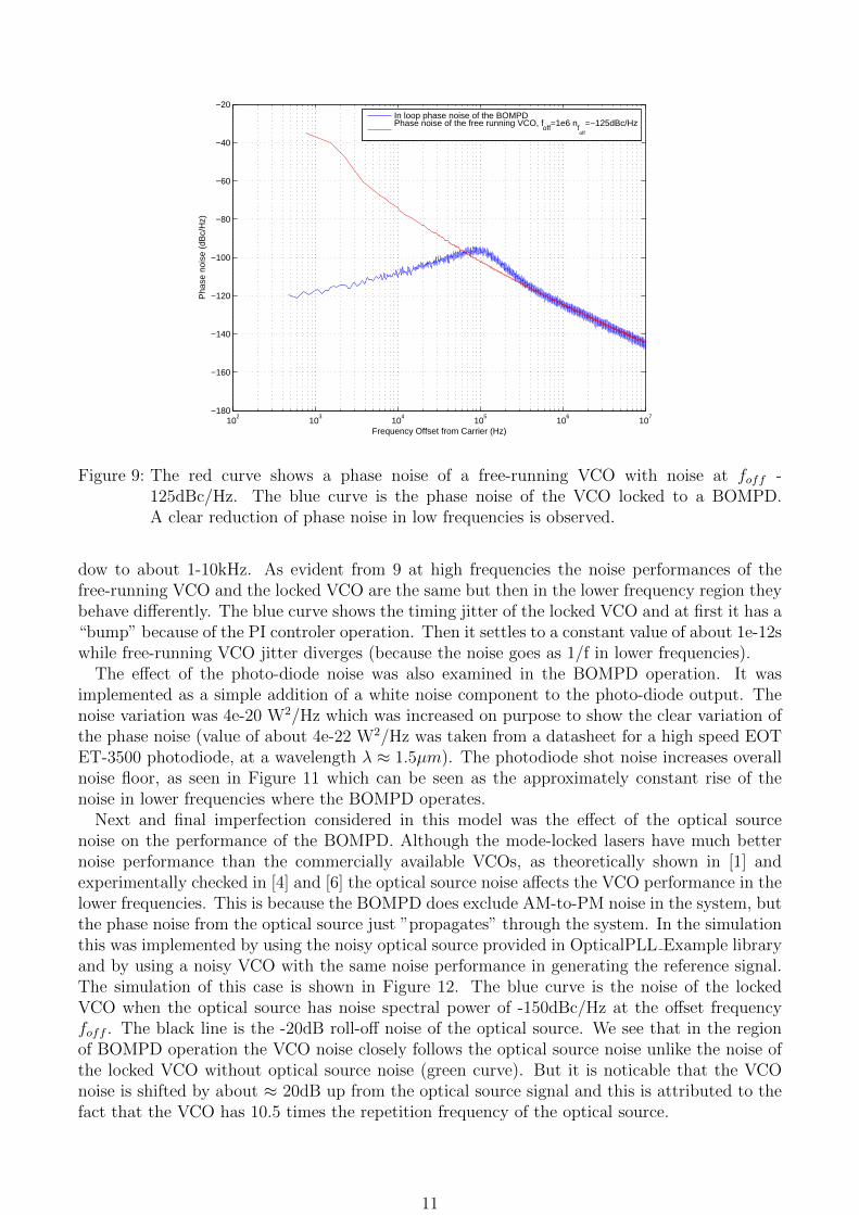
Figure 9: The red curve shows a phase noise of a free-running VCO with noise at foff -125dBc/Hz. The blue curve is the phase noise of the VCO locked to a BOMPD.A clear reduction of phase noise in low frequencies is observed.
dow to about 1-10kHz. As evident from 9 at high frequencies the noise performances of thefree-running VCO and the locked VCO are the same but then in the lower frequency region theybehave differently. The blue curve shows the timing jitter of the locked VCO and at first it has a“bump” because of the PI controler operation. Then it settles to a constant value of about 1e-12swhile free-running VCO jitter diverges (because the noise goes as 1/f in lower frequencies).
The effect of the photo-diode noise was also examined in the BOMPD operation. It wasimplemented as a simple addition of a white noise component to the photo-diode output. Thenoise variation was 4e-20 W2/Hz which was increased on purpose to show the clear variation ofthe phase noise (value of about 4e-22 W2/Hz was taken from a datasheet for a high speed EOTET-3500 photodiode, at a wavelength λ ≈ 1.5µm). The photodiode shot noise increases overallnoise floor, as seen in Figure 11 which can be seen as the approximately constant rise of thenoise in lower frequencies where the BOMPD operates.
Next and final imperfection considered in this model was the effect of the optical sourcenoise on the performance of the BOMPD. Although the mode-locked lasers have much betternoise performance than the commercially available VCOs, as theoretically shown in [1] andexperimentally checked in [4] and [6] the optical source noise affects the VCO performance in thelower frequencies. This is because the BOMPD does exclude AM-to-PM noise in the system, butthe phase noise from the optical source just ”propagates” through the system. In the simulationthis was implemented by using the noisy optical source provided in OpticalPLL Example libraryand by using a noisy VCO with the same noise performance in generating the reference signal.The simulation of this case is shown in Figure 12. The blue curve is the noise of the lockedVCO when the optical source has noise spectral power of -150dBc/Hz at the offset frequencyfoff . The black line is the -20dB roll-off noise of the optical source. We see that in the regionof BOMPD operation the VCO noise closely follows the optical source noise unlike the noise ofthe locked VCO without optical source noise (green curve). But it is noticable that the VCOnoise is shifted by about ≈ 20dB up from the optical source signal and this is attributed to thefact that the VCO has 10.5 times the repetition frequency of the optical source.
11

103
104
105
106
107
0
0.5
1
1.5
2
2.5
3x 10
−12
Frequency [Hz]
Inte
grat
ed ti
min
g jit
ter
[s]
Integrated timing jitter of a BOMPDIntegrated timing jitter of a free−running VCO
Figure 10: The red curve shows integrated timing jitter from 10Mhz of a free-running VCO withnoise spectral denisty -125dBc/Hz at foff . The blue curve is the integrated timingjitter of a VCO connected with a BOMPD.
6 Conclusion
In this report the results of a summer student programe done in DESY during the summer of2014 was presented. An accurate and robust simulation of a Balanced Optical-Microwave PhaseDetector was implemented in the systems simulation package CppSim. A simplified model of aBOMPD was implemented and in the perfect case without any noise sources it was shown thatit locks the VCO output signal to the optical signal perfectly. Imperfections were introducedby considering the noise sources in the system. Main noise source in the system is the phasenoise of a free running VCO. It was shown that this noise is successfuly attenuated in the lowfrequency region by the BOMPD, in this simple model. Then the effect of the shot noise inthe photo-detection process and the effect of the optical source noise was considered and shownto be in agreement with qualitative considerations. The BOMPD simulation shows a proof ofconcept and it should be possible to extend the model to get quantitative results in agreementwith the experiment. The model of the BOMPD is also easily extendible such that a complicatedimplementation can be done e.g. by including noise in the amplification stages or non-linearitiesin the Sagnac loop. This could enable a complete simulation of experimental results such asAM-to-PM supression ratio in [7] and could even help with new experimental results in thefuture.
I would like to thank my supervisor Aram Kalaydzhyan for a great help and guidance throughthis project and the group leader Franz Kartner for hosting me Ultrafast Optics and X-RaysDivision. I would also like to thank the whole crew of the DESY summer program 2014 as thissummer wouldn’t be as good and fun without them.
12

104
105
106
107
108
−180
−170
−160
−150
−140
−130
−120
−110
−100
−90The effect of diode shot noise on the BOMPD phase noise
Frequency Offset from Carrier (Hz)
Out
put S
pect
rum
(dB
c/H
z)
BOMPD without diode shot noise, f
off=1e6 n
off=−125dBc/Hz
BOMPD with shot noise, power 4e−20 W2/Hz, foff
=1e6 noff
=−125dBc/Hz
Figure 11: The blue curve is the phase noise of a BOMPD without shot-noise in the diode. Redcurve is the phase noise of a BOMPD when a shot noise of variation 4e-20 W2/Hz isapplied to the photo-diode output.
102
103
104
105
106
107
−180
−160
−140
−120
−100
−80
−60
−40
−20
Frequency Offset from Carrier (Hz)
Pha
se n
oise
(dB
c/H
z)
Phase noise of a free−running VCOBOMPD phase noise with included optical source noise, −150dBc/Hz at f
off=1e6Hz
Optical source noise floorBOMPD phase noise withouit optical source noise
Figure 12: The red curve represents the phase noise of a free-running VCO with noise -125dBc/Hz at 1MHz. The blue green curve is the phase noise of a VCO with noise-125dBc/Hz at 1MHz locked to a BOMPD. The blue curve is the noise of a VCOlocked to the BOMPD with noisy optical source, with noise -150dBc/Hz at 1Mhz.The black line is the phas noise of the optical source. We can clearly see that thenoise of the BOMPD output follows the optical source noise at low frequencies butwith a shift of ≈ 20dB which is atributed to 10.5 times higher frequency of the VCOto the optical source.
13
References
[1] J. Kim and F. X. Kartner, “Attosecond-precision ultrafast photonics,” Laser Photonics Rev4, 421-456 (2010).
[2] A. Bartels et. al., “Femtosecond-laser-based synthesis of ultrastable microwave signals fromoptical frequency references,” Opt. Lett. 30, 667 (2005).
[3] J. Kim, F. X. Kartner, and M. H. Perrott, “Femtosecond synchronization of radio frequencysignals with optical pulse trains,” Opt. Lett. 29, 2076 (2004).
[4] J. Kim, F.X. Kartner, and F. Ludwig, “Balanced opticalmicrowave phase detectors foroptoelectronic phase-locked loops,” Opt. Lett. 31, 3659 (2006).
[5] J. Kim, F. Ludwig, M. Felber, and F.X. Kartner, “Long-term stable microwave signalextraction from mode-locked lasers,” Opt. Express 15, 8951 (2007).
[6] J. Kim, J. A. Cox, J. Chen, and F. X. Kartner, “Drift-free femtosecond timing synchro-nization of remote optical and microwave sources,” Nature Photon. 2, 733 (2008).
[7] M. Y. Peng, A. Kalaydzhyan, and F.X. Kartner, “Balanced Optical-Microwave Phase De-tector for Sub-Femtosecond Optical-RF Synchronization,” - Manuscript submitted for pub-lication.
[8] M.H. Perrott, “CppSim System Simulator Package,” http://www.cppsim.com.
[9] M.H. Perrott, “Fast and Accurate Behavioral Simulation of Fractional-N Synthesizers andother PLL/DLL Circuits,” Design Automation Conference (DAC), 2002, pp 498-503.
[10] M.H. Perrott, “CppSim Reference Manual Version 5.3,” http://www.cppsim.com.
14
Related Documents


![ALL-OPTICAL MICROWAVE SIGNAL PROCESSING€¦ · Microwave photonics is an interdisciplinary field that investigates the interaction between microwave and optical signals [1]-[3] for](https://static.cupdf.com/doc/110x72/60833e506ba8f8072e7ce524/all-optical-microwave-signal-processing-microwave-photonics-is-an-interdisciplinary.jpg)


