NUC970 Jan. 27, 2015 Nuvoton Technology Corp.

NUC970 Jan. 27, 2015 Nuvoton Technology Corp.. 2 Power on setting Power-On Setting Pin Description Power-On Setting Register Bit USB0_IDUSB Port 0 Role.
Jan 12, 2016
Welcome message from author
This document is posted to help you gain knowledge. Please leave a comment to let me know what you think about it! Share it to your friends and learn new things together.
Transcript
NUC970
Jan. 27, 2015
Nuvoton Technology Corp.
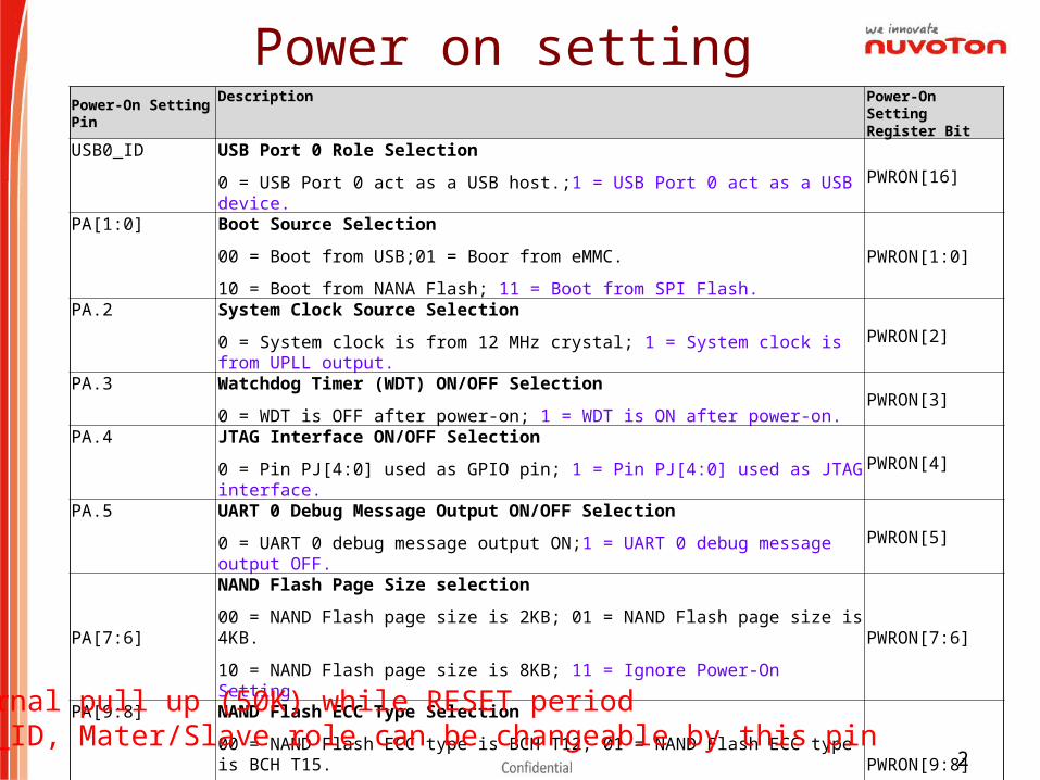
2
Power on setting Power-On Setting Pin
Description Power-On Setting Register Bit
USB0_ID USB Port 0 Role Selection
0 = USB Port 0 act as a USB host.;1 = USB Port 0 act as a USB device.PWRON[16]
PA[1:0] Boot Source Selection
00 = Boot from USB;01 = Boor from eMMC.
10 = Boot from NANA Flash; 11 = Boot from SPI Flash.
PWRON[1:0]
PA.2 System Clock Source Selection
0 = System clock is from 12 MHz crystal; 1 = System clock is from UPLL output.PWRON[2]
PA.3 Watchdog Timer (WDT) ON/OFF Selection
0 = WDT is OFF after power-on; 1 = WDT is ON after power-on.PWRON[3]
PA.4 JTAG Interface ON/OFF Selection
0 = Pin PJ[4:0] used as GPIO pin; 1 = Pin PJ[4:0] used as JTAG interface.PWRON[4]
PA.5 UART 0 Debug Message Output ON/OFF Selection
0 = UART 0 debug message output ON;1 = UART 0 debug message output OFF.PWRON[5]
PA[7:6]
NAND Flash Page Size selection
00 = NAND Flash page size is 2KB; 01 = NAND Flash page size is 4KB.
10 = NAND Flash page size is 8KB; 11 = Ignore Power-On Setting.
PWRON[7:6]
PA[9:8] NAND Flash ECC Type Selection
00 = NAND Flash ECC type is BCH T12; 01 = NAND Flash ECC type is BCH T15.
10 = NAND Flash ECC type is BCH T24; 11 = Ignore Power-On Setting.
PWRON[9:8]
Internal pull up (50K) while RESET periodUSB0_ID, Mater/Slave role can be changeable by this pin

3
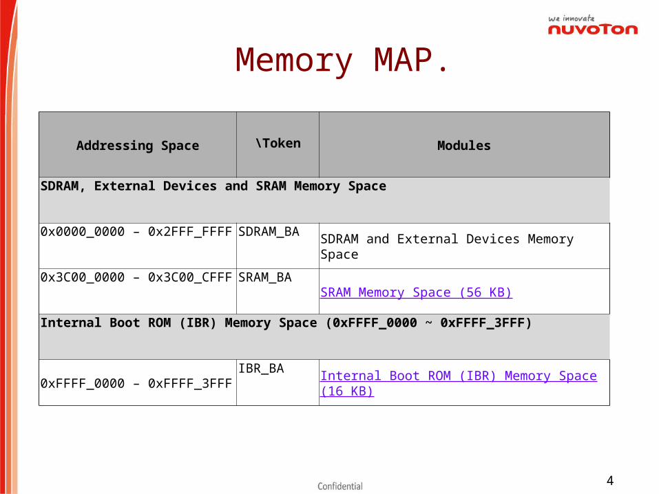
System Memory Map
4
Memory MAP.
Addressing Space \Token Modules
SDRAM, External Devices and SRAM Memory Space
0x0000_0000 – 0x2FFF_FFFF SDRAM_BASDRAM and External Devices Memory Space
0x3C00_0000 – 0x3C00_CFFF SRAM_BASRAM Memory Space (56 KB)
Internal Boot ROM (IBR) Memory Space (0xFFFF_0000 ~ 0xFFFF_3FFF)
0xFFFF_0000 – 0xFFFF_3FFFIBR_BA
Internal Boot ROM (IBR) Memory Space (16 KB)

5
AHB Reg. MAP
AHB Modules Memory Space (0xB000_0000 – 0xB7FF_FFFF)
0xB000_0000 – 0xB000_01FF SYS_BA System Global Control Registers
0xB000_0200 – 0xB000_02FF CLK_BA Clock Control Registers
0xB000_1000 – 0xB000_17FF EBI_BA EBI Control Registers
0xB000_1800 – 0xB000_1FFF SDIC_BA SDRAM (SDR/DDR/DDR2) Control Registers
0xB000_2000 – 0xB000_2FFF EMAC0_BA Ethernet MAC 0 Control Registers
0xB000_3000 – 0xB000_3FFF EMAC1_BA Ethernet MAC 1 Control Registers
0xB000_4000 – 0xB000_4FFF GDMA_BA GDMA Control Registers
0xB000_5000 – 0xB000_5FFF EHCI_BA USB EHCI Host Control Registers
0xB000_6000 – 0xB000_6FFF USBD_BA USB Device Control Registers
0xB000_7000 – 0xB000_7FFF OHCI_BA USB OHCI Host Control Registers
0xB000_8000 – 0xB000_8FFF LCD_BA LCD Display Control Registers
0xB000_9000 – 0xB000_9FFF I2S_BA I2S Interface Control Registers
0xB000_A000 – 0xB000_AFFF JPEG_BA JPEG Codec Control Registers
0xB000_B000 – 0xB000_BFFF GE2D_BA 2D Graphic Engine Control Registers
0xB000_C000 – 0xB000_CFFF SDIO_BA SD/SDIO Host Control Registers
0xB000_D000 – 0xB000_DFFF FMI_BA Flash Memory Interface (FMI) Control Registers
0xB000_E000 – 0xB000_EFFF VCAP_BA Video Capture (CMOS Sensor Interface) Control Registers
0xB000_F000 – 0xB000_FFFF CRYPTO_BA Cryptographic Accelerator Control Registers

6
APB MAPAPB Modules Memory Space (0xB800_0000 ~ 0xBBFF_FFFF)0xB800_0000 – 0xB800_00FF UART0_BA UART 0 Control Registers0xB800_0100 – 0xB800_01FF UART1_BA UART 1 Control Registers (High-Speed UART)0xB800_0200 – 0xB800_02FF UART2_BA UART 2 Control Registers (High-Speed UART)0xB800_0300 – 0xB800_03FF UART3_BA UART 3 Control Registers0xB800_0400 – 0xB800_04FF UART4_BA UART 4 Control Registers (High-Speed UART)0xB800_0500 – 0xB800_05FF UART5_BA UART 5 Control Registers0xB800_0600 – 0xB800_06FF UART6_BA UART 6 Control Registers (High-Speed UART)0xB800_0700 – 0xB800_07FF UART7_BA UART 7 Control Registers0xB800_0800 – 0xB800_08FF UART8_BA UART 8 Control Registers (High-Speed UART)0xB800_0900 – 0xB800_09FF UART9_BA UART 9 Control Registers0xB800_0A00 – 0xB800_0AFF UART10_BA UART 10 Control Registers (High-Speed UART)0xB800_1000 – 0xB800_10FF TIMER_BA Timer Control Registers0xB800_1400 – 0xB800_14FF ETIMER0_BA Enhance Timer 0 Control Registers0xB800_1500 – 0xB800_15FF ETIMER1_BA Enhance Timer 1 Control Registers0xB800_1600 – 0xB800_16FF ETIMER2_BA Enhance Timer 2 Control Registers0xB800_1700 – 0xB800_17FF ETIMER3_BA Enhance Timer 3 Control Registers0xB800_1800 – 0xB800_18FF WDT_BA Watch-Dog Timer Control Registers0xB800_1900 – 0xB800_19FF WWDT_BA Windowed Watch-Dog Timer Control Registers0xB800_2000 – 0xB800_2FFF AIC_BA Advance Interrupt Control Registers0xB800_3000 – 0xB800_3FFF GPIO_BA GPIO Control Registers0xB800_4000 – 0xB800_4FFF RTC_BA Real Time Clock (RTC) Control Registers0xB800_5000 – 0xB800_53FF SC0_BA Smart Card 0 Control Registers0xB800_5400 – 0xB800_57FF SC1_BA Smart Card 1 Control Registers0xB800_6000 – 0xB800_60FF I2C0_BA I2C 0 Control Registers0xB800_6100 – 0xB800_61FF I2C1_BA I2C 1 Control Registers0xB800_6200 – 0xB800_62FF SPI0_BA SPI 0 Control Registers0xB800_6300 – 0xB800_63FF SPI1_BA SPI 1 Control Registers0xB800_7000 – 0xB800_7FFF PWM_BA PWM Control Registers0xB800_8000 – 0xB800_8FFF KPI_BA KPI Control Registers0xB800_A000 – 0xB800_AFFF ADC_BA ADC Control Registers0xB800_B000 – 0xB800_B3FF CAN0_BA CAN 0 Control Registers0xB800_B400 – 0xB800_B7FF CAN1_BA CAN 1 Control Registers0xB800_C000 – 0xB800_CFFF MTP_BA MTP Control Registers (OTP)
7
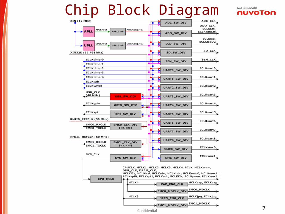
Chip Block Diagram

8
NUC970 Features (1)NUC970 Features (1)
CoreARM® ARM926EJ-S™ processor core runs up to 300 MHz
Support 16 KB instruction cache and 16 KB data cache
Support MMU
Support JTAG Debug interface
External Bus Interface (EBI)Support SRAM and external I/O devices
Support 8/16-bit data bus width
Up to 5 chip selects for SRAM or external I/O devices
Programmable access cycle
4 x 32-bit write buffers
(Don’t support SDRAM & NOR)
9
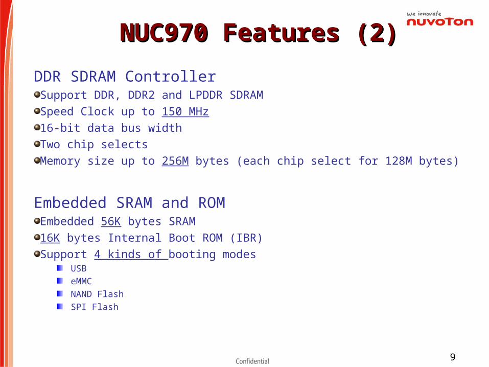
NUC970 Features (2)NUC970 Features (2)
DDR SDRAM ControllerSupport DDR, DDR2 and LPDDR SDRAM
Speed Clock up to 150 MHz
16-bit data bus width
Two chip selects
Memory size up to 256M bytes (each chip select for 128M bytes)
Embedded SRAM and ROMEmbedded 56K bytes SRAM
16K bytes Internal Boot ROM (IBR)
Support 4 kinds of booting modesUSB
eMMC
NAND Flash
SPI Flash
10
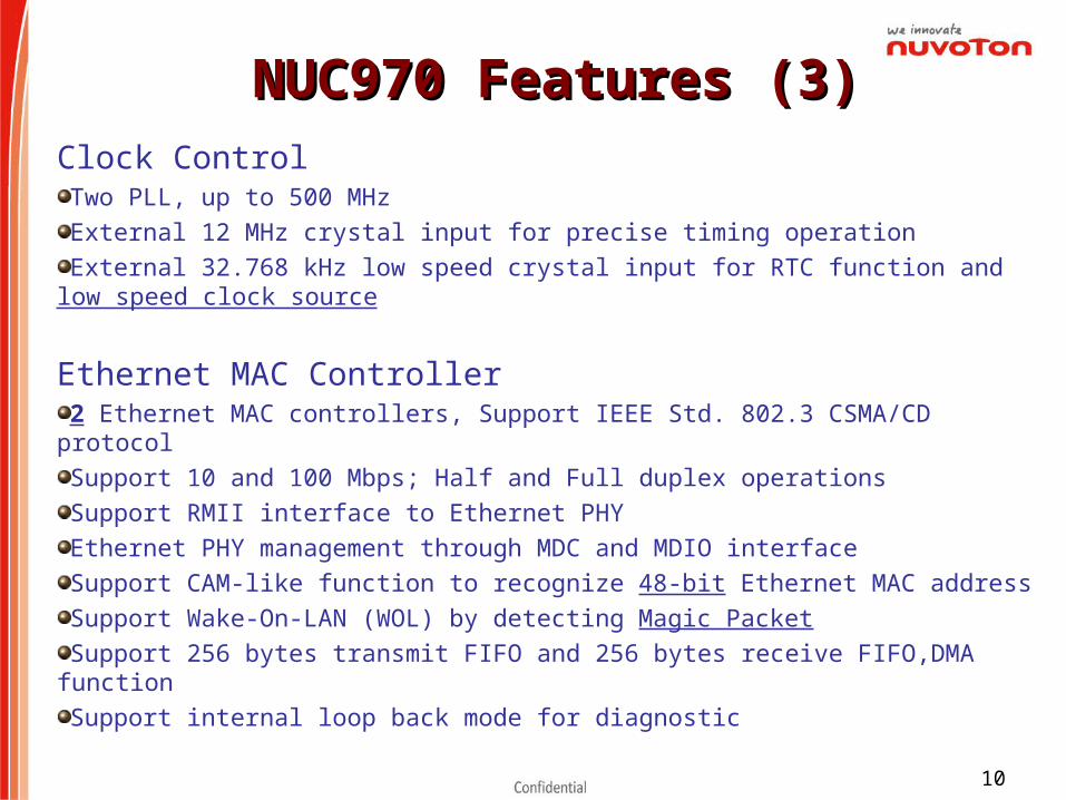
NUC970 Features (3)NUC970 Features (3)
Clock ControlTwo PLL, up to 500 MHz
External 12 MHz crystal input for precise timing operation
External 32.768 kHz low speed crystal input for RTC function and low speed clock source
Ethernet MAC Controller2 Ethernet MAC controllers, Support IEEE Std. 802.3 CSMA/CD protocol
Support 10 and 100 Mbps; Half and Full duplex operations
Support RMII interface to Ethernet PHY
Ethernet PHY management through MDC and MDIO interface
Support CAM-like function to recognize 48-bit Ethernet MAC address
Support Wake-On-LAN (WOL) by detecting Magic Packet
Support 256 bytes transmit FIFO and 256 bytes receive FIFO,DMA function
Support internal loop back mode for diagnostic
11
NUC970 Features (4)NUC970 Features (4)
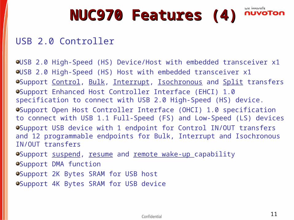
USB 2.0 Controller
USB 2.0 High-Speed (HS) Device/Host with embedded transceiver x1
USB 2.0 High-Speed (HS) Host with embedded transceiver x1
Support Control, Bulk, Interrupt, Isochronous and Split transfers
Support Enhanced Host Controller Interface (EHCI) 1.0 specification to connect with USB 2.0 High-Speed (HS) device.
Support Open Host Controller Interface (OHCI) 1.0 specification to connect with USB 1.1 Full-Speed (FS) and Low-Speed (LS) devices
Support USB device with 1 endpoint for Control IN/OUT transfers and 12 programmable endpoints for Bulk, Interrupt and Isochronous IN/OUT transfers
Support suspend, resume and remote wake-up capability
Support DMA function
Support 2K Bytes SRAM for USB host
Support 4K Bytes SRAM for USB device
12
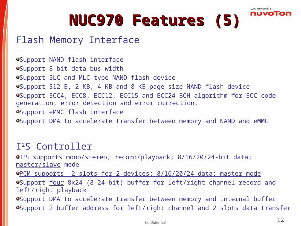
NUC970 Features (5)NUC970 Features (5)Flash Memory Interface
Support NAND flash interface
Support 8-bit data bus width
Support SLC and MLC type NAND flash device
Support 512 B, 2 KB, 4 KB and 8 KB page size NAND flash device
Support ECC4, ECC8, ECC12, ECC15 and ECC24 BCH algorithm for ECC code generation, error detection and error correction.
Support eMMC flash interface
Support DMA to accelerate transfer between memory and NAND and eMMC
I2S ControllerI2S supports mono/stereo; record/playback; 8/16/20/24-bit data; master/slave mode
PCM supports 2 slots for 2 devices; 8/16/20/24 data; master mode
Support four 8x24 (8 24-bit) buffer for left/right channel record and left/right playback
Support DMA to accelerate transfer between memory and internal buffer
Support 2 buffer address for left/right channel and 2 slots data transfer

13
NUC970 Features (6)NUC970 Features (6)
LCD Display Controller
Support 8/12/16/18/24-bit data to connect 80/68 mode MPU type LCD
Support resolution up to 2048x2048
Data format conversion for display output
From RGB444, RGB565, RGB666, RGB888, YUV422 and YUV444 to
RGB444, RGB565, RGB666, RGB888, YUV422 and YUV444
Support CCIR-656 with VSYNC, HSYNC and data enable sync signal,
8/16-bit YUV data output to connect with external TV encoder
Support 8/16 bpp OSD data with video overlay
Support linear 1X to 8X image scaling up function
Support Picture-In-Picture display function
Support hardware cursor
14
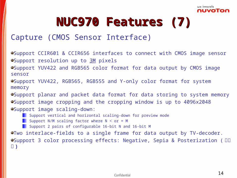
NUC970 Features (7)NUC970 Features (7)Capture (CMOS Sensor Interface)
Support CCIR601 & CCIR656 interfaces to connect with CMOS image sensor
Support resolution up to 3M pixels
Support YUV422 and RGB565 color format for data output by CMOS image sensor
Support YUV422, RGB565, RGB555 and Y-only color format for system memory
Support planar and packet data format for data storing to system memory
Support image cropping and the cropping window is up to 4096x2048
Support image scaling-down:Support vertical and horizontal scaling-down for preview mode
Support N/M scaling factor where N < or = M
Support 2 pairs of configurable 16-bit N and 16-bit M
Two interlace-fields to a single frame for data output by TV-decoder.
Support 3 color processing effects: Negative, Sepia & Posterization (海報化 )

15
NUC970 Features (8)NUC970 Features (8)
2D Graphic Engine
Support 2D Bit Block Transfer (BitBLT) functions defined in Microsoft GDI
Support Host, Pattern, Color/Font Expanding, Transparent, Tile, Block Move,Copy File BLT
Support Color/Font Expansion, Rectangle Fill
Support RGB332/RGB565/RGB888 data format.
Support fore/background colors and all Microsoft 256 ternary raster-operation codes (ROP)
Support both inside and outside clipping function
Support alpha-blending for source/destination picture overlaying
Support fast Bresenham line drawing algorithm to draw solid/textured line 用來描繪由兩點所決定的直線的演算法Support rectangular border and frame drawing, picture re-sizing
Support down-scaling from 1/255 to 254/255;up-scaling from 1 to 1.996 (1+254/255)
Support object rotation with different degree
Support L45 (45 degree left rotation) and L90 (90 degree left rotation)
Support R45 (45 degree right rotation) and R90 (90 degree right rotation)
Support M180 (mirror/flop)
Support F180 (up-side-down (flip) and X180 (180 degree rotation)

16
NUC970 Features (9)NUC970 Features (9)JPEG CodecBaseline Sequential mode, compliant with ISO/IEC 10918-1 international JPEG standard
Planar FormatSupport encode interleaved YCbCr 4:2:2/4:2:0 and gray-level (Y only) format image
Support decode interleaved YCbCr 4:4:4/4:2:2/4:2:0/4:1:1 and gray-level (Y only) format image
Support decode YCbCr 4:2:2 transpose format
Support arbitrary width and height image encode and decode
Support three programmable quantization-tables
Support standard default Huffman-table and programmable Huffman-table for decode
Support arbitrarily 1X~8X image up-scaling function for encode mode
Support down-scaling function for encode and decode modes
Support specified window decode mode
Support quantization-table adjustment for bit-rate and quality control in encode mode
Support rotate function in encode mode
Packet FormatSupport encode interleaved YUYV format input image, output bit stream 4:2:2 and 4:2:0 format
Support to decode interleaved YCbCr 4:4:4/4:2:2/4:2:0 format image
Support decoded output image RGB555, RGB565 and RGB888 formats.
The encoded JPEG bit-stream format is fully compatible with JFIF and EXIF standards
Support arbitrary width and height image encode and decode
Support three programmable quantization-tables
Support standard default Huffman-table and programmable Huffman-table for decode
Support arbitrarily 1X~8X image up-scaling function for encode mode
Support down-scaling function 1X~ 16X for Y422 and Y420, 1X~ 8X for Y444 for decode mode
Support specified window decode mode
Support quantization-table adjustment for bit-rate and quality control in encode mode
Support Scatter-Gather mode for output frame buffer
17
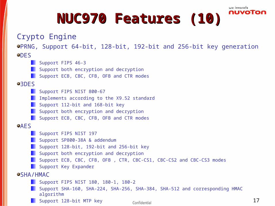
NUC970 Features (10)NUC970 Features (10)Crypto Engine PRNG, Support 64-bit, 128-bit, 192-bit and 256-bit key generation
DESSupport FIPS 46-3
Support both encryption and decryption
Support ECB, CBC, CFB, OFB and CTR modes
3DESSupport FIPS NIST 800-67
Implements according to the X9.52 standard
Support 112-bit and 168-bit key
Support both encryption and decryption
Support ECB, CBC, CFB, OFB and CTR modes
AESSupport FIPS NIST 197
Support SP800-38A & addendum
Support 128-bit, 192-bit and 256-bit key
Support both encryption and decryption
Support ECB, CBC, CFB, OFB , CTR, CBC-CS1, CBC-CS2 and CBC-CS3 modes
Support Key Expander
SHA/HMACSupport FIPS NIST 180, 180-1, 180-2
Support SHA-160, SHA-224, SHA-256, SHA-384, SHA-512 and corresponding HMAC algorithm
Support 128-bit MTP key

18
NUC970 Features (11)NUC970 Features (11)
GDMA (General DMA)Support 2 channels GDMA for memory-to-memory data transfer without CPU intervention
Support increment and decrement for source and destination address calculation
Support 8-bit, 16-bit and 32-bit width data transfer
Support four 8-bit/16-bit/32-bit burst transfer
UARTSupport up to 11 UART controllers
Support 1 UART (UART1) with full model function (TXD/RXD/CTS/RTS/CDn/Rin/DTR/ DSR) and 64-byte FIFO
Support 5 UART (UART2/4/6/8/10) with flow control (TXD/RXD/CTS/RTS) and 64-byte FIFO
Support 5 TXD/RXD only UART ports (UART 0/3/5/7/9) with 16-byte FIFO for standard device
Support IrDA (SIR) and LIN function
Support RS-485 9-bit mode and direction control
Support programmable baud-rate generator up to 1/16 system clock
19
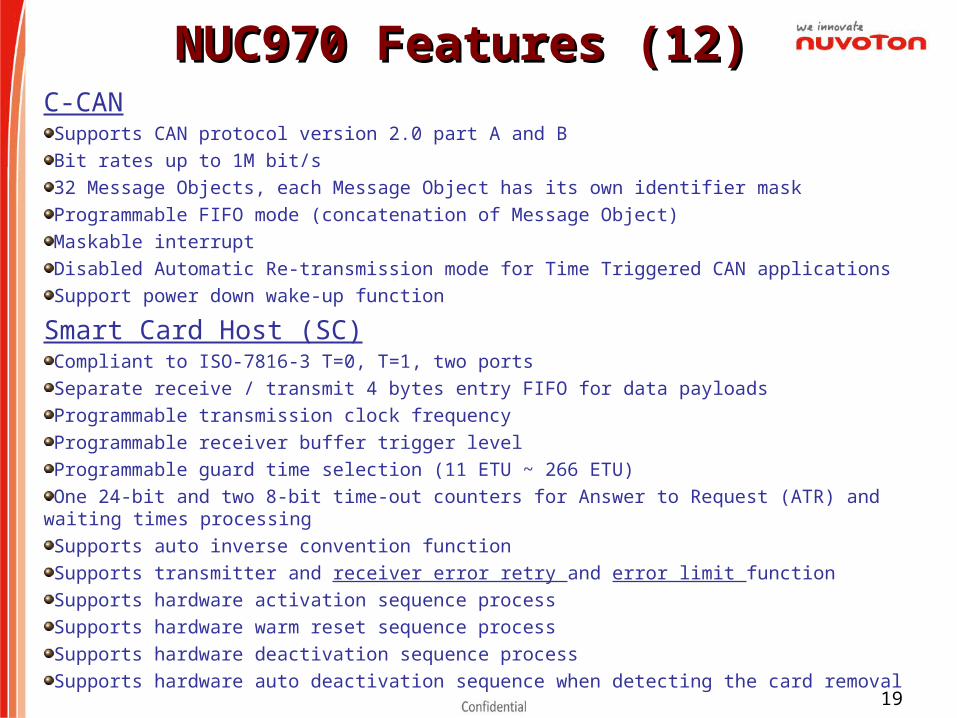
NUC970 Features (12)NUC970 Features (12)C-CANSupports CAN protocol version 2.0 part A and B
Bit rates up to 1M bit/s
32 Message Objects, each Message Object has its own identifier mask
Programmable FIFO mode (concatenation of Message Object)
Maskable interrupt
Disabled Automatic Re-transmission mode for Time Triggered CAN applications
Support power down wake-up function
Smart Card Host (SC)Compliant to ISO-7816-3 T=0, T=1, two ports
Separate receive / transmit 4 bytes entry FIFO for data payloads
Programmable transmission clock frequency
Programmable receiver buffer trigger level
Programmable guard time selection (11 ETU ~ 266 ETU)
One 24-bit and two 8-bit time-out counters for Answer to Request (ATR) and waiting times processing
Supports auto inverse convention function
Supports transmitter and receiver error retry and error limit function
Supports hardware activation sequence process
Supports hardware warm reset sequence process
Supports hardware deactivation sequence process
Supports hardware auto deactivation sequence when detecting the card removal

20
NUC970 Features (13)NUC970 Features (13)TimerSupport 5 sets of 32-bit timers with 24-bit up-timer and one 8-bit pre-scale counter
Independent clock source for each timer
Support one-shot, periodic, toggle and continuous operation modes
Enhanced TimerSupport 4 sets of 32-bit timers with 24-bit up-timer and one 8-bit pre-scale counter
Independent clock source for each timer
Support one-shot, periodic, toggle and continuous operation modes
Supports external pin capture for interval measurement
Supports external pin capture for timer counter reset
Watchdog TimerMultiple clock sources
8 selectable time out period from 1.6ms ~ 26.0sec (depends on clock source)
WDT can wake-up from power down or idle mode
Interrupt or reset selectable on watchdog timer time-out
Windowed-Watchdog Timer6-bit down counter with 11-bit pre-scale for wide range window selected
Interrupt on windowed-watchdog timer time-out
Reset on windowed-watchdog timer time out or reload in an unexpected time window
21
NUC970 Features (14)NUC970 Features (14)
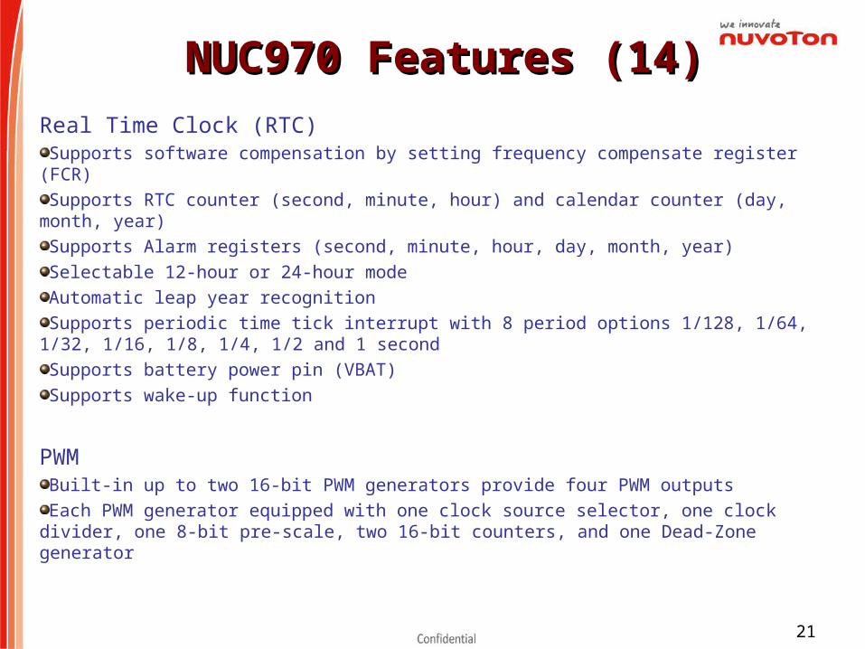
Real Time Clock (RTC) Supports software compensation by setting frequency compensate register (FCR)
Supports RTC counter (second, minute, hour) and calendar counter (day, month, year)
Supports Alarm registers (second, minute, hour, day, month, year)
Selectable 12-hour or 24-hour mode
Automatic leap year recognition
Supports periodic time tick interrupt with 8 period options 1/128, 1/64, 1/32, 1/16, 1/8, 1/4, 1/2 and 1 second
Supports battery power pin (VBAT)
Supports wake-up function
PWMBuilt-in up to two 16-bit PWM generators provide four PWM outputs
Each PWM generator equipped with one clock source selector, one clock divider, one 8-bit pre-scale, two 16-bit counters, and one Dead-Zone generator
22
NUC970 Features (15)NUC970 Features (15)SPIBuilt-in up to two sets of SPI controller
Support SPI master mode
Support single/dual/quad bit data bus width
Full duplex synchronous serial data transfer
Variable length of transfer data from 8 to 32 bits
MSB or LSB first data transfer
Burst mode operation that transmission and reception can be executed up to 4 times in a transfer
Support 2 slave/device select lines
I2CTwo sets of I2C engines support master mode
Bidirectional data transfer between masters and slaves
Multi-master bus (no central master)
Arbitration between simultaneously transmitting masters without corruption of serial data on the bus
Serial clock synchronization allows devices with different bit rates to communicate via one serial bus
Serial clock synchronization can be used as a handshake mechanism to suspend and resume serial transfer
Programmable clocks allow versatile rate control
Support software mode to generate I2C signaling

23
NUC970 Features (16)NUC970 Features (16)Advanced Interrupt ControllerSupport 58 interrupt sources, including 8 external interrupt sources
Support programmable normal or fast interrupt mode (IRQ, FIQ)
Support programmable edge-triggered or level-sensitive for 8 external interrupt sources
Support programmable low-active or high-active for 8 external interrupt sources
Support encoded priority methodology to allow for interrupt daisy-chaining
Support lower priority interrupt automatically mask out for nested interrupt
Support to clear interrupt flag automatically if interrupt source is programmed as edge-triggered
GPIOTTL/Schmitt trigger input selectable
I/O pin can be configured as interrupt source with edge/level setting
Support pull-up and pull-down control
ADC12-bit SAR ADC with 1M/200K SPS
Up to 8-ch single-end input
Support 4-wire or 5-wire resistance touch screen interface
Support touch pressure (Z) measurement for 4-wire touch screen application
Support pen down detection
Support battery measurement
Support keypad scan

24
NUC970 Features (17)NUC970 Features (17)KPI ( It cannot be shared with LCD) Matrix keypad interface supported.
Maximum 4X8 and minimum 3X3 keypad matrix supported.
Configurable key de-bounce supported.
Low power wakeup mode supported.
Configurable three-key reset supported.
MTP (OTP)Support 256-bit programmable memory for key of Crypto functionality
Support up to 15 times of programming and erase.
TIC (it can support MTP programming) SPI-Like slave interface supported for test purpose.
1-bit, 2-bit and 4-bit data width supported.
Single and burst (four 32-bit data) data access supported.
DTS only, don’t release in TRM
25
NUC970 Features (18)NUC970 Features (18)
Low Voltage Detect and Reset (VSI IP)Support two, 2.6V and 2.8V, voltage detection levels
Interrupt when low voltage detected
Reset when low voltage detected
Low Voltage Reset threshold voltage levels: 2.4 V
Operating Voltage1.2V for core logic operating
1.8V/2.5V/3.3V for DDR2/DDR/SDR SDRAM I/O operating
3.3V for normal I/O operating
Operating Temperature: -40 ~85℃ ℃
Packages: All Green package (RoHS)LQFP 216-pin
LQFP 128-pin

26
PKG Naming Rule

27
Key Components Function Key Material pcs/board Note
1 RS232TRS3232EC 6Female connector 5
2 CANTi SN65HVD230 3.3-V CAN TRANSCEIVERS 2Connector 2
3 IIS NAU8822L 14 Key SW Tack switch 32 Temprary
LCDPanel, E50A2V1 5” with TP (800x480) 140-pin, bottom 1
6 NAND Winbond, 1G 17 JTAG ICE Multi-ICE 10x2 pins DIN connector 1
8 Etherneta).EMAC PHY, IC+ 101GR 1b).RJ45 w LED 1c).Transformer 1
10 SD Normal STD SD slot 1
11 USB hosta).Host TYP A connector 1b).USB5V Power OCP, APL3511A 1
12 USB device Mini. B Device connector 1
13 CMOS sensorNT99141, 720P 1FPC 24-pin w/ Bottom side. 1
14 eMMC ASiP NCMMCA04A 1
17 BatteryCR2032 1battery paddle 1
18 Smart card Smart card slot 119 SPI flash Winbond SPI 16MB Flash
28
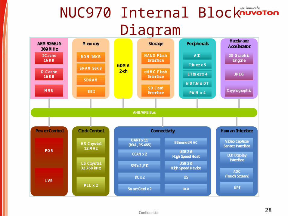
NUC970 Internal Block DiagramARM926EJ-S
300 MHz
GDMA2-ch
Power Control Clock Control Connectivity
AHB/APB Bus
Memory
I-Cache16 KB
D-Cache16 KB
MMU
ROM 16KB
EBI
SDRAM
SRAM 56KB
POR
HS Crystal12 MHz
LVR
LS Crystal32.768 kHz
PLL x 2
UART x 11(IrDA, RS-485)
I2SI2C x 2
SPI x 2, PIC
CCAN x 2
USB 2.0High Speed Device
USB 2.0 High Speed Host
Ethernet MAC
Smart Card x 2 SDIO
Human Interface
Video CaptureSensor Interface
KPI
ADC(Touch Screen)
LCD Display Interface
Peripherals
AIC
Storage
NAND FlashInterface
SD CardInterface
Hardware Accelerator
2D GraphicEngine
eMMC FlashInterface
PWM x 4
WDT/WWDT
Timer x 5
ETimer x 4
Cryptographic
JPEG
ARM926EJ-S300 MHz
GDMA2-ch
Power Control Clock Control Connectivity
AHB/APB Bus
Memory
I-Cache16 KB
D-Cache16 KB
MMU
ROM 16KB
EBI
SDRAM
SRAM 56KB
POR
HS Crystal12 MHz
LVR
LS Crystal32.768 kHz
PLL x 2
UART x 11(IrDA, RS-485)
I2SI2C x 2
SPI x 2, PIC
CCAN x 2
USB 2.0High Speed Device
USB 2.0 High Speed Host
Ethernet MAC
Smart Card x 2 SDIO
Human Interface
Video CaptureSensor Interface
KPI
ADC(Touch Screen)
LCD Display Interface
Peripherals
AIC
Storage
NAND FlashInterface
SD CardInterface
Hardware Accelerator
2D GraphicEngine
eMMC FlashInterface
PWM x 4
WDT/WWDT
Timer x 5
ETimer x 4
Cryptographic
JPEG

29
Function NUC976 NUC977 NUC972 NUC973
PKG LQFP128 LQFP128 LQFP216 LQFP216
EBI x x V V
SAR_ADC TP(4) x TP(4/5)+AIN(4/3) TP(4)+AIN(1)
NAND x V V V
Video CAP V V V V
USBH+USBD V V V V
SPISPI0(4-bit)SPI1(1-bit)
SPI0(4-bit) two CSSPI1(1-bit) two CS
SPI0(4-bit)two CSSPI1(4-bit)two CS
SPI0(4-bit)two CSSPI1(4-bit)two CS
LCD 16-bit 16-bit 24-bit 24-bit
Smartcard SMCx2 SMCx2 SMCx2 SMCx2
CAN CANx1 CANx1 CANx2 CANx2
LAN RMIIx1 RMIIx1 RMIIx2 RMIIx2
UART Port 0,6,8 &10 Port 0, 5,6,7,8 & 10 All-11 All-11
SD 2 ports 2 ports 2 ports 2 ports
eMMC (4-bit) V V V V
I2C 2 2 2 2
I2S V V V V
KPI 4x8 4x8 4x8 4x8
RTC V V V V
Application2D-Bar code/finger Printer
HMI/ Industrial Power Meter POS
NUC970 Series
30
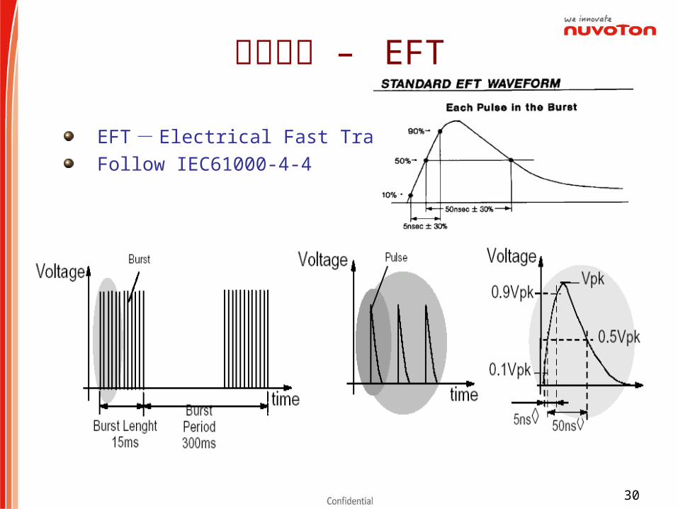
電氣特性 – EFT
EFT - Electrical Fast Transients
Follow IEC61000-4-4

31
Nuvoton MCU EFT Test Environment
DC5V
Keytek EMCpro DC5V CoupleEFT Noise
NUC972
VDD
VSS
VDD
0.1uF4.7uF
XT1_IN
XT1_OUT
12MHz
/RESET
VDD
1uF
10K
4KV EFT Noise
Follow IEC61000-4-4
32
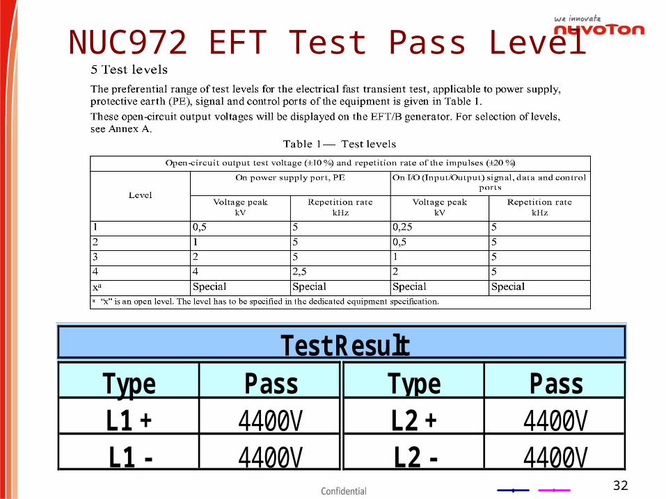
NUC972 EFT Test Pass Level
Type Pass Type PassL1 + 4400V L2 + 4400VL1 - 4400V L2 - 4400V
Test Result
0
0.2
0.4
0.6
0.8
1
1.2
0
#REF! #REF!

33
和可靠度相关的电气特性 – Chip ESD3 种不同的 Chip ESD
HBMHBM(Human-Body Model)(Human-Body Model)
MMMM(Machine Model)(Machine Model)
CDMCDM(Charged-Device Model)(Charged-Device Model)
200V
0V
0V
2000V
0V
500V

34
Chip ESD 和 System ESD 是不一样的规格标准不同
Chip ESD: HBM MIL-STD-833C, MM: EIA/JESD22-A115-A
System ESD: IEC 61000-4-2
应用场合不同Chip ESD: 芯片未上电 , 应用于生产 , 运送中的保护System ESD: 芯片上电 , 应用于实际工作状态
能量等级不同Chip ESD: HBM 2KV, MM 200V 是一般 IC level
System ESD Level 4: Contact Mode 8KV, Air Mode 15KV
System ESD 只靠 MPU 檔不住 , 需外部保護元件
• Under 8-kV ESD zapping, the peak current in system-level ESD test is about 5 ~ 6 times larger than that in component-level ESD test
35
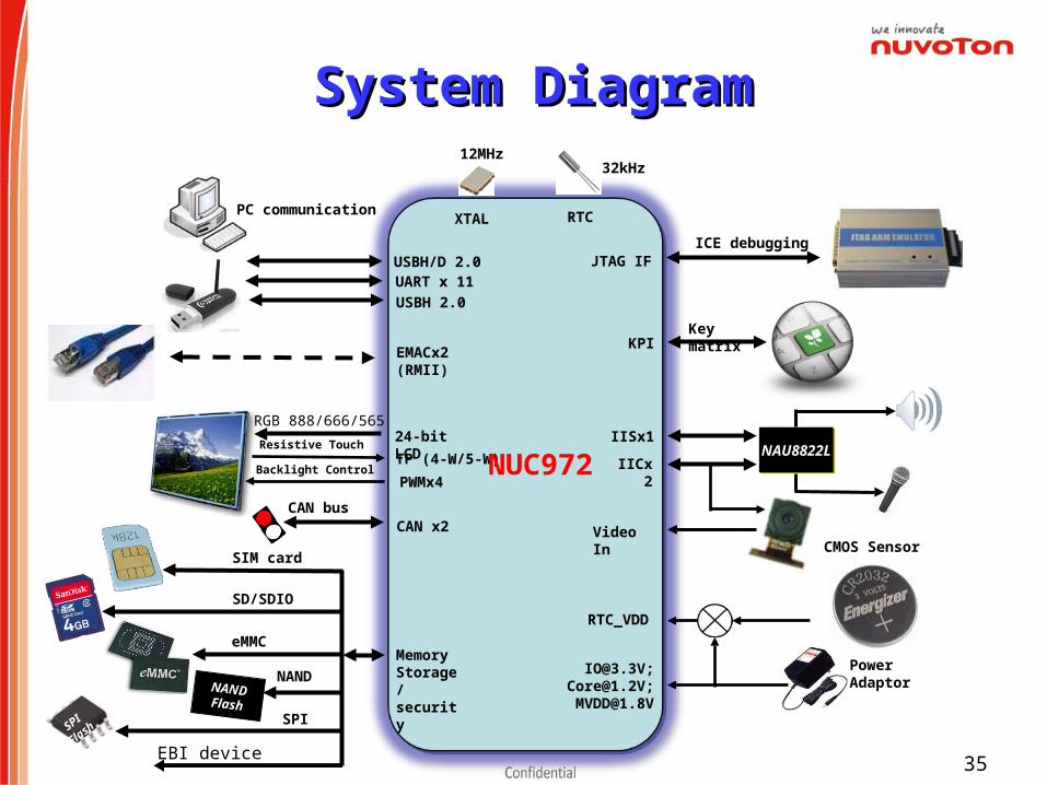
System DiagramSystem Diagram
JTAG IF USBH/D 2.0
USBH 2.0
Video In
IISx1
TP (4-W/5-W)
RTC
PWMx4
24-bit LCD
KPI
RTC_VDD
NAU8822LNAU8822L
12MHz
NUC972Resistive Touch
Backlight Control
Power Adaptor
CMOS Sensor
Key matrix
PC communication
[email protected]; [email protected];
ICE debugging
IICx2
SPI
Flash
MemoryStorage/security NAND
Flash
SIM card
CAN x2
XTAL
32kHz
UART x 11
EMACx2 (RMII)
SD/SDIO
eMMC
NAND
SPI
CAN bus
EBI device
RGB 888/666/565

36
NUC970 System Power SchemeNUC970 System Power Scheme
Core1.2V (PLL)
USBPLL0_1.2V
USBPLL1_1.2V
USB0_3.3V
USB1_3.3V
SAR_ADC_3.3V
IO3.3V
Vin
PowerON/OFF
RTC_3.3V
Vin
BAT
NUC972 RTC_WKUP

37
Related Documents