NTHU-CS VLSI/CAD LAB TH EDA TH EDA De-Shiuan Chiou De-Shiuan Chiou Da-Cheng Juan Da-Cheng Juan Yu-Ting Chen Yu-Ting Chen Shih-Chieh Chang Shih-Chieh Chang Department of CS, National Tsing Hua University, Taiwan Fine-Grained Sleep Transistor Sizing Algorithm for Leakage Power Minimization

Welcome message from author
This document is posted to help you gain knowledge. Please leave a comment to let me know what you think about it! Share it to your friends and learn new things together.
Transcript

NTHU-CS VLSI/CAD LAB
TH EDATH EDA
De-Shiuan ChiouDe-Shiuan ChiouDa-Cheng JuanDa-Cheng JuanYu-Ting ChenYu-Ting Chen
Shih-Chieh ChangShih-Chieh Chang
Department of CS, National Tsing Hua University, Taiwan
Fine-Grained Sleep Transistor Sizing Algorithm for Leakage Power Minimization
Fine-Grained Sleep Transistor Sizing Algorithm for Leakage Power Minimization

2
OutlineOutline
Sleep Transistor Sizing ProblemSleep Transistor Sizing Problem
MIC Estimation MechanismMIC Estimation Mechanism
Partitioned Time-Frame for MIC EstimationPartitioned Time-Frame for MIC Estimation
Experimental Results and ConclusionsExperimental Results and Conclusions

3
Power GatingPower Gating
Leakage increases exponentiallyLeakage increases exponentially– reach 50% of total power in 65nm technologyreach 50% of total power in 65nm technology
Power GatingPower Gating– One of the most effective ways to reduce leakage reduce leakage
Low Vth Logic Device
VDD
GNDuse high Vth Sleep Transistorto reduce the leakage current
SLVGND
GND

4
C1 C2 C3
Implementation of Power GatingImplementation of Power Gating
Distributed Sleep Transistor Network (DSTN)Distributed Sleep Transistor Network (DSTN)
VDD
VGND
Low Vth Logic Device
SL SL SL

5
Leakage SavingLeakage Saving
In standby mode:In standby mode:– Leakage: Leakage: proportionalproportional to the ST’s size to the ST’s size– Small ST to reduce leakageSmall ST to reduce leakage
Ileakage
VDD
VGND
Ileakage Ileakage

6
Voltage Drop across the STVoltage Drop across the ST
In active mode:In active mode:– Voltage drop across a ST degrades the speedVoltage drop across a ST degrades the speed– Voltage drop: Voltage drop: inversely proportionalinversely proportional to the ST’s size to the ST’s size– Large ST to bound the voltage dropLarge ST to bound the voltage drop
VST
VDD
VGND
VST VST

7
VST* VST*
Sleep Transistor (ST) SizingSleep Transistor (ST) Sizing
Dilemma scenario:Dilemma scenario:– LargeLarge ST to bound the voltage drop. (active mode) ST to bound the voltage drop. (active mode)– SmallSmall ST to reduce leakage. (standby mode) ST to reduce leakage. (standby mode)
=>objective: =>objective: minimize ST size (leakage) under a specified minimize ST size (leakage) under a specified voltage drop constraint, voltage drop constraint, VVSTST**
VST
VDD
VGND
VST VSTVST*

8
C1 C2 C3
Estimate Voltage Drop by MICEstimate Voltage Drop by MIC
Maximum Instantaneous Current (MIC)Maximum Instantaneous Current (MIC) through the ST through the ST– determines the worst case voltage dropdetermines the worst case voltage drop
Estimating the upper bound of MIC(ST)Estimating the upper bound of MIC(ST)– for sizing ST appropriately to meet voltage drop constraintfor sizing ST appropriately to meet voltage drop constraint
MIC(ST1)
VDD
VGNDMIC(ST2) MIC(ST3)
MIC(ST): MIC across a ST.

9
C1 C2 C3
Estimate Voltage Drop by MICEstimate Voltage Drop by MIC
MICMIC((CC) (MIC of a cluster) is easy to measure) (MIC of a cluster) is easy to measure Due to current balancing effectDue to current balancing effect
– MICMIC((STST) (MIC through the ST) is hard to predict) (MIC through the ST) is hard to predict
MIC(ST1)
VDD
VGNDMIC(ST2) MIC(ST3)
MIC(C1)
Finding the MIC of a cluster is
fast
Finding the MIC across a ST is time-
consuming

10
Temporal Perspective of Clusters’ MICTemporal Perspective of Clusters’ MIC
Traditional ways Traditional ways – use the use the entire clock period’s MICentire clock period’s MIC
to determine the ST sizeto determine the ST size
(Time Unit)
Cluster 1Cluster 2
MIC(C2) occurs at T9
one clock cycle
MIC(Ci) waveform
(Curr
ent)
MIC(C1) occurs at T6

11
(Time Unit)
Curr
ent
(mA
)
Cluster 1Cluster 2
Temporal Perspective of Clusters’ MICTemporal Perspective of Clusters’ MIC
one clock cycle
MIC(Ci) waveform
Smaller time frames leads to:Smaller time frames leads to:– a more accurate MIC estimationa more accurate MIC estimation– high computation complexityhigh computation complexity
12
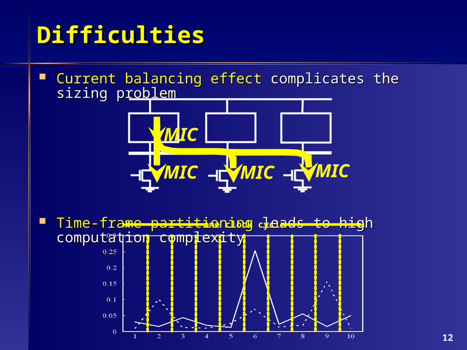
DifficultiesDifficulties
Current balancing effectCurrent balancing effect complicates the sizing problem complicates the sizing problem
Time-frame partitioningTime-frame partitioning leads to high computation complexity leads to high computation complexity
MIC MIC MIC
MIC
one clock cycle

13
ContributionsContributions
A more accurate MIC prediction in a A more accurate MIC prediction in a temporal perspectivetemporal perspective
A A variable-length variable-length partitioning to reduce computation partitioning to reduce computation complexitycomplexity
Heuristics to minimize the size of sleep transistorsHeuristics to minimize the size of sleep transistors
Achieving 21% reduction in sleep transistor areaAchieving 21% reduction in sleep transistor area

14
OutlineOutline
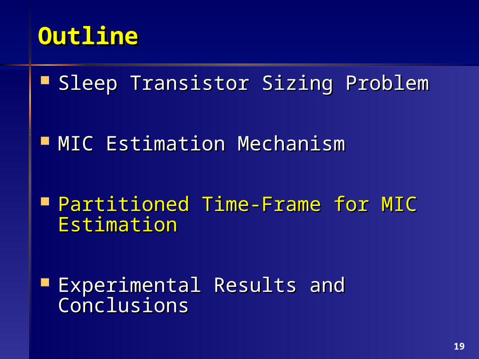
Sleep Transistor Sizing ProblemSleep Transistor Sizing Problem
MIC Estimation MechanismMIC Estimation Mechanism
Partitioned Time-Frame for MIC EstimationPartitioned Time-Frame for MIC Estimation
Experimental Results and ConclusionsExperimental Results and Conclusions
15
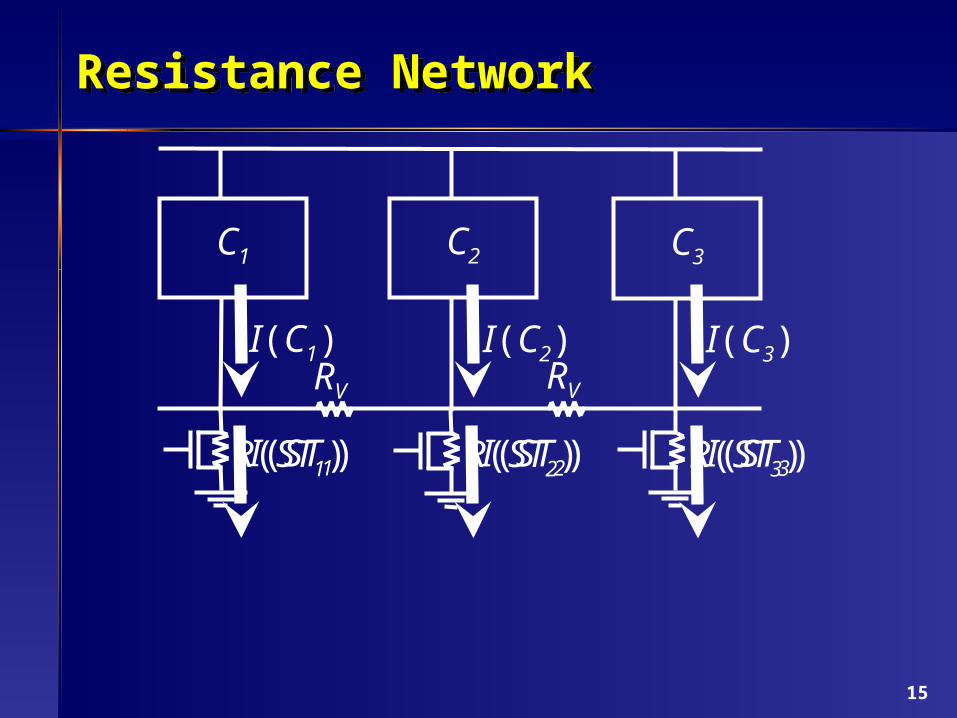
Resistance NetworkResistance Network
I(ST1) I(ST2) I(ST3)
I(C1) I(C2) I(C3)
R(ST1) R(ST2) R(ST3)
RV RV
C1 C2 C3

16
The discharging ratio can be calculated byThe discharging ratio can be calculated by– Kirchhoff’s Current LawKirchhoff’s Current Law– Ohm’s LawOhm’s Law
Discharging RatioDischarging Ratio
9 8 10
2 2
C1 C2 C3
0.43 I(C1) 0.34 I(C2) 0.23 I(C3)
I(C1)

17
Discharging Matrix ΨDischarging Matrix Ψ
)(
)(
)(
)(
)(
)(
3
2
1
3
2
1
CI
CI
CI
Ψ
STI
STI
STI
→
333231
232221
131211
ψψψ
ψψψ
ψψψ
Ψwhere
I(ST1) I(ST2) I(ST3)
I(C1) I(C2) I(C3)
C1 C2 C3

18
MIC(ST) Estimation MechanismMIC(ST) Estimation Mechanism
)(
)(
)(
)(
)(
)(
3
2
1
3
2
1
CMIC
CMIC
CMIC
Ψ
STMIC
STMIC
STMIC
→
MIC(ST1) MIC(ST2) MIC(ST3)
MIC(C1) MIC(C2) MIC(C3)
C1 C2 C3
333231
232221
131211
ψψψ
ψψψ
ψψψ
Ψwhere
19
OutlineOutline
Sleep Transistor Sizing ProblemSleep Transistor Sizing Problem
MIC Estimation MechanismMIC Estimation Mechanism
Partitioned Time-Frame for MIC EstimationPartitioned Time-Frame for MIC Estimation
Experimental Results and ConclusionsExperimental Results and Conclusions

20
Temporal Perspective of Clusters’ MICTemporal Perspective of Clusters’ MIC
Different MIC(Ci) occurs at different time points
(Time Unit)
Cluster 1Cluster 2
MIC(C2) occurs at T9
one clock cycle
MIC(Ci) waveform
(Curr
ent)
MIC(C1) occurs at T6

21
Temporal Perspective of Clusters’ MICTemporal Perspective of Clusters’ MIC
)(
)(
)(
)(
)(
)(
3
2
1
3
2
1
CMIC
CMIC
CMIC
Ψ
STMIC
STMIC
STMIC
Different MIC(Ci) occurs at different time points within a clock period
Traditional way to estimate MIC(STi) is over pessimistic

22
Time-Frame Partitioning for MIC(ST) EstimationTime-Frame Partitioning for MIC(ST) Estimation
Expand MIC(Ci) into MIC(Ci,Tj)
(Time Frame)
Cluster 1Cluster 2
one clock cycle
MIC(Ci,Tj) waveform
(Curr
ent)
MIC(C1,T1)
MIC(C2,T1)
MIC(C1,T3)
MIC(C2,T3)
MIC(C1,T6)
MIC(C2,T6)

23
For each time frame Tj, use MIC(Ci,Tj) to obtain MIC(STi,Tj)
( , ) ( , )
( , ) ( , )
( , ) ( , )
1 1 1 1
2 1 2 1
3 1 3 1
MIC ST T MIC C T
MIC ST T Ψ MIC C T
MIC ST T MIC C T
Time-Frame Partitioning for MIC(ST) EstimationTime-Frame Partitioning for MIC(ST) Estimation

24
Time-Frame Partitioning for MIC(ST) EstimationTime-Frame Partitioning for MIC(ST) Estimation
For ST1, the maximum MIC(ST1,Tj) among all Tj is the upper bound of MIC(ST1) after partitioning
Cluster 1Cluster 2
(Time Frame)
one clock cycle
MIC(STi,Tj) waveform
MIC(ST1)
ST 1ST 2
(Curr
ent)
MIC(ST2)

25
Time-Frame Partitioning for MIC(ST) EstimationTime-Frame Partitioning for MIC(ST) Estimation
Cluster 1Cluster 2
(Time Frame)
one clock cycle
MIC(STi,Tj) waveform
MIC(ST1)
ST 1ST 2
MIC(ST2)
(Curr
ent)
ORIGINAL_MIC(ST1
) 37% larger!
ORIGINAL_MIC(ST2
)27% larger!
Time-Frame Partitioning leads to a better MIC(ST) estimation!

26
Reduce the Computation ComplexityReduce the Computation Complexity
Increase the number of time frames leads toIncrease the number of time frames leads to– more accurate voltage drop estimationmore accurate voltage drop estimation– high computation complexityhigh computation complexity
Reduce the computation complexity:Reduce the computation complexity:– dominated time-frame removaldominated time-frame removal– variable length time-frame partitioningvariable length time-frame partitioning

27
Dominated Time-Frame RemovalDominated Time-Frame Removal
TT33 is dominated by is dominated by TT66
– MICMIC((CC11,T,T66)) > MIC > MIC((CC11,T,T33))– MICMIC((CC22,T,T66)) > MIC > MIC((CC22,T,T33))
NeglectNeglect T T33 and all dominated time and all dominated time framesframes
Cluster 1Cluster 2
MIC(C1,T6)
MIC(C1,T3)
MIC(C2,T6)
MIC(C2,T3)

28
((TTbb dominates dominates TTcc ) and () and (TTbb dominates dominates TTdd))=> the estimated upper bound will be smaller=> the estimated upper bound will be smaller
If all the If all the MICMIC((CCii) are separated, the ) are separated, the MICMIC((STSTii) can be better ) can be better estimated!estimated!
Variable Length Time-Frame PartitioningVariable Length Time-Frame Partitioning
Ta
uniform two-way partition variable length two-way partition
Tb TdTc
MIC(C1,Tb)
MIC(C2,Tb)
MIC(C1,Td)
MIC(C2,Td)
MIC(C1,Tc)
MIC(C2,Tc)
(1) (2)

29
Problem Formulation of ST SizingProblem Formulation of ST Sizing
Inputs:Inputs:1.1. Voltage-drop constraintVoltage-drop constraint
2.2. MICMIC((CCii,,TTjj): Clusters’ MIC information): Clusters’ MIC information
Objective: minimize the total ST widthObjective: minimize the total ST width
Voltage drops must meet the constraintVoltage drops must meet the constraint

30
ST Sizing AlgorithmST Sizing Algorithm
99 99 9999
1. Initialize ST size with a large value.
MIC(STi,Tj)= . MIC(Ci,Tj)V(STi,Tj)=MIC(STi,Tj) . R(STi
)
3. Update MIC(STi,Tj) and voltage drops.
Ψ
Return ST size
Yes
Voltage drops ok?
0.38 0.30 0.21 0.18
0.27 0.30 0.21 0.18
0.21 0.24 0.35 0.28
0.14 0.16 0.23 0.36
=Ψ
2. Update the discharging matrix.
No
4. Resize ST with the worst drop.
99 73 9999
kV
TSTMICW
ST
jiST )
*
),((*

31
OutlineOutline
Sleep Transistor Sizing ProblemSleep Transistor Sizing Problem
MIC Estimation MechanismMIC Estimation Mechanism
Partitioned Time-Frame for MIC EstimationPartitioned Time-Frame for MIC Estimation
Experimental Results and ConclusionsExperimental Results and Conclusions

32
Environment SetupEnvironment Setup
TSMC 130nm CMOS technologyTSMC 130nm CMOS technology
Vdd = 1.3 voltVdd = 1.3 volt
Specified tolerable IR drop: Specified tolerable IR drop: 5% of the ideal supply voltage5% of the ideal supply voltage
MICMIC((CCii,T,Tjj) is obtained via 10,000-random-pattern ) is obtained via 10,000-random-pattern PrimePower simulationsPrimePower simulations

33
Implementation FlowImplementation Flow
RTL netlist
SDF file
Gate Positioning
Gate location
VCD Partitioning
Partitioned VCD file
: Our tools
: Commercial tools
Synthesis
Gate-level netlist
MIC Estimation
V-length Partitioning (Optional)
ST sizeST Sizing
Simulation
VCD file
Placement
DEF file

34
Experimental ResultsExperimental Results
Avg.
AES
des
t481
i8
frg2
dalu
C7552
C5315
C3540
C1355
C880
C499
C432
Circuit
1 8.09 1.06 1 1.26 1.70
35242837928137272293396544378
1180832181457850976611804
1514162895402502473899405
1080772081417836993113247
1367012255223228353632
48338162283211029043468
28961721625621242692950041016
21901383019534187852377329794
9421685620282186502302029808
422251411496105911305619352
3452561967692331129615050
568364472296684834710741
495426270866775849112817
V-TPTPV-TPTP[2][8]
Runtime (Sec.)Total Area (Width in μm)
Previous works: [2] Chiou et al. DAC’06, [8] Long et al. DAC’03

35
ConclusionsConclusions
Propose an efficient sleep transistor sizing method Propose an efficient sleep transistor sizing method for DSTN power gating designsfor DSTN power gating designs
Present theorems based on Present theorems based on temporal perspectivetemporal perspective for for estimating a tight upper bound of voltage dropestimating a tight upper bound of voltage drop
Achieving 21% size (leakage) reductionAchieving 21% size (leakage) reduction

36
Thank You!Thank You!

37
Sleep Transistor (ST) SizingSleep Transistor (ST) Sizing
Relations between Relations between WWSTST, and , and VVSTST..
Sleep Transistors operate in Sleep Transistors operate in linear regionlinear region in active in active mode.mode.
kV
STIW
STST )
)((
VDD
VGND
GND
I(ST)
I(ST): the current through the sleep
transistor
VST
VST: the voltage drop across the sleep transistor

38
Sleep Transistor (ST) SizingSleep Transistor (ST) Sizing
Determine the Determine the minimum required sizeminimum required size ( (WWSTST** ) ) based on:based on:1.1. MICMIC((STST))
2.2. VVSTST**:: IR-drop constraintIR-drop constraint
kV
STMICW
STST )
*
)((*
VDD
VGND
GND
MIC(ST)
MIC(ST): Maximum Instantaneous Current (MIC) through STk
V
STIW
STST )
)((
Smaller MIC(ST) leads to a better ST size!
Related Documents