San Jose State University San Jose State University SJSU ScholarWorks SJSU ScholarWorks Master's Theses Master's Theses and Graduate Research Spring 2013 Novel Systematic Phase Noise Reduction Techniques for Phase Novel Systematic Phase Noise Reduction Techniques for Phase Interpolator Clock and Data Recovery Interpolator Clock and Data Recovery Yu Feng San Jose State University Follow this and additional works at: https://scholarworks.sjsu.edu/etd_theses Recommended Citation Recommended Citation Feng, Yu, "Novel Systematic Phase Noise Reduction Techniques for Phase Interpolator Clock and Data Recovery" (2013). Master's Theses. 4272. DOI: https://doi.org/10.31979/etd.r5ax-2vqv https://scholarworks.sjsu.edu/etd_theses/4272 This Thesis is brought to you for free and open access by the Master's Theses and Graduate Research at SJSU ScholarWorks. It has been accepted for inclusion in Master's Theses by an authorized administrator of SJSU ScholarWorks. For more information, please contact [email protected].

Welcome message from author
This document is posted to help you gain knowledge. Please leave a comment to let me know what you think about it! Share it to your friends and learn new things together.
Transcript
San Jose State University San Jose State University
SJSU ScholarWorks SJSU ScholarWorks
Master's Theses Master's Theses and Graduate Research
Spring 2013
Novel Systematic Phase Noise Reduction Techniques for Phase Novel Systematic Phase Noise Reduction Techniques for Phase
Interpolator Clock and Data Recovery Interpolator Clock and Data Recovery
Yu Feng San Jose State University
Follow this and additional works at: https://scholarworks.sjsu.edu/etd_theses
Recommended Citation Recommended Citation Feng, Yu, "Novel Systematic Phase Noise Reduction Techniques for Phase Interpolator Clock and Data Recovery" (2013). Master's Theses. 4272. DOI: https://doi.org/10.31979/etd.r5ax-2vqv https://scholarworks.sjsu.edu/etd_theses/4272
This Thesis is brought to you for free and open access by the Master's Theses and Graduate Research at SJSU ScholarWorks. It has been accepted for inclusion in Master's Theses by an authorized administrator of SJSU ScholarWorks. For more information, please contact [email protected].
NOVEL SYSTEMATIC PHASE NOISE REDUCTION TECHNIQUES
FOR PHASE INTERPOLATOR CLOCK AND DATA RECOVERY
A Thesis
Presented to
The Faculty of the Department of Electrical Engineering
San José State University
In Partial Fulfillment
of the Requirements for the Degree
Master of Science
by
Yu M. Feng
May 2013

© 2013
Yu M. Feng
ALL RIGHTS RESERVED

The Designated Thesis Committee Approves the Thesis Titled
NOVEL SYSTEMATIC PHASE NOISE REDUCTION TECHNIQUES
FOR PHASE INTERPOLATOR CLOCK AND DATA RECOVERY
by
Yu M. Feng
APPROVED FOR THE DEPARTMENT OF ELECTRICAL ENGINEERING
SAN JOSÉ STATE UNIVERSITY
May 2013
Dr. Shahab Ardalan Department of Electrical Engineering
Dr. Sotoudeh Hamedi-Hagh Department of Electrical Engineering
Prof. Morris Jones Department of Electrical Engineering

ABSTRACT
NOVEL SYSTEMATIC PHASE NOISE REDUCTION TECHNIQUES
FOR PHASE INTERPOLATOR CLOCK AND DATA RECOVERY
by Yu M. Feng
This work focused on high-speed source-synchronous clock and multi-channel data
receivers for inter-chip communications. Designs of inter-chip communication are
becoming increasingly difficult with the rise in clock rates and the reduction in voltage
supplies. Data transmissions at rates of gigabits per second require a fast and accurate
clock and data recovery system on the front end of receivers.
Many designs allow for source-synchronous clocking architectures, but this work
focused on a dual-loop with a phase-locked loop for frequency tracking and phase
integrators for tracking each individual data lane. Limitations with the phase interpolator
architecture cause systematic jitter, reducing the data eye.
Various techniques exist that aim to reduce or eliminate this systematic jitter from
phase interpolator architectures. A technique based on digital lock detection was
developed for this work that eliminates the phase interpolator systematic jitter.

v
ACKNOLWEDGEMENTS
I would very much like to extend my gratitude towards Dr. Shahab Ardalan for his
guidance and feedback throughout this research. You have challenged my mind to expand
my thinking into more abstract and system-oriented terms. I find myself gleaning deeper
meaning from all my past education with this new mindset. My only regret is not being
able to show you more of my ability in design and leaving a taped-out parting gift.
I am grateful for having such great colleagues at Dr. Ardalan’s AMS lab. I cannot
even count the number of times where bouncing ideas off of one another has led to
different angles with which to approach roadblocks in thinking.
This thesis would never have reached much cohesion or any semblance of concise
thinking had Angelo Volpe not nearly failed me in freshman composition. A large part of
my success in this field is from submitting short, compact reports. I continue to spread his
style of persuasive and argumentative writing with each keystroke and each paper I
proofread.
Finally, I reserve my most profound appreciation for my family. Without the daily
distractions provided by my dear sisters, brothers, and cousins, this work would have been
completed years ago. However, accomplishing that without you guys behind me would
have been meaningless. My education in this field would also have never amounted to
much without the unwavering push from my parents. This work is dedicated to all the
warmth and support I have received from all of you.
vi
TABLE OF CONTENTS
Chapter 1. Introduction ............................................................................................... 1
1.1. Clock and Data Recovery ...................................................................................... 2
1.1.1. Phase Interpolator ........................................................................................... 3
1.1.2. Systematic Jitter .............................................................................................. 4
1.2. Motivation ............................................................................................................. 4
1.3. Organization .......................................................................................................... 5
Chapter 2. Background ................................................................................................ 6
2.1. Phase-Locked Loops.............................................................................................. 6
2.1.1. Phase-Frequency Detector .............................................................................. 7
2.1.1.1. Linear Detector ......................................................................................... 8
2.1.1.2. Binary Detector ...................................................................................... 10
2.1.2. Charge Pump and Loop Filter ....................................................................... 11
2.1.3. Voltage-Controlled Oscillator ....................................................................... 13
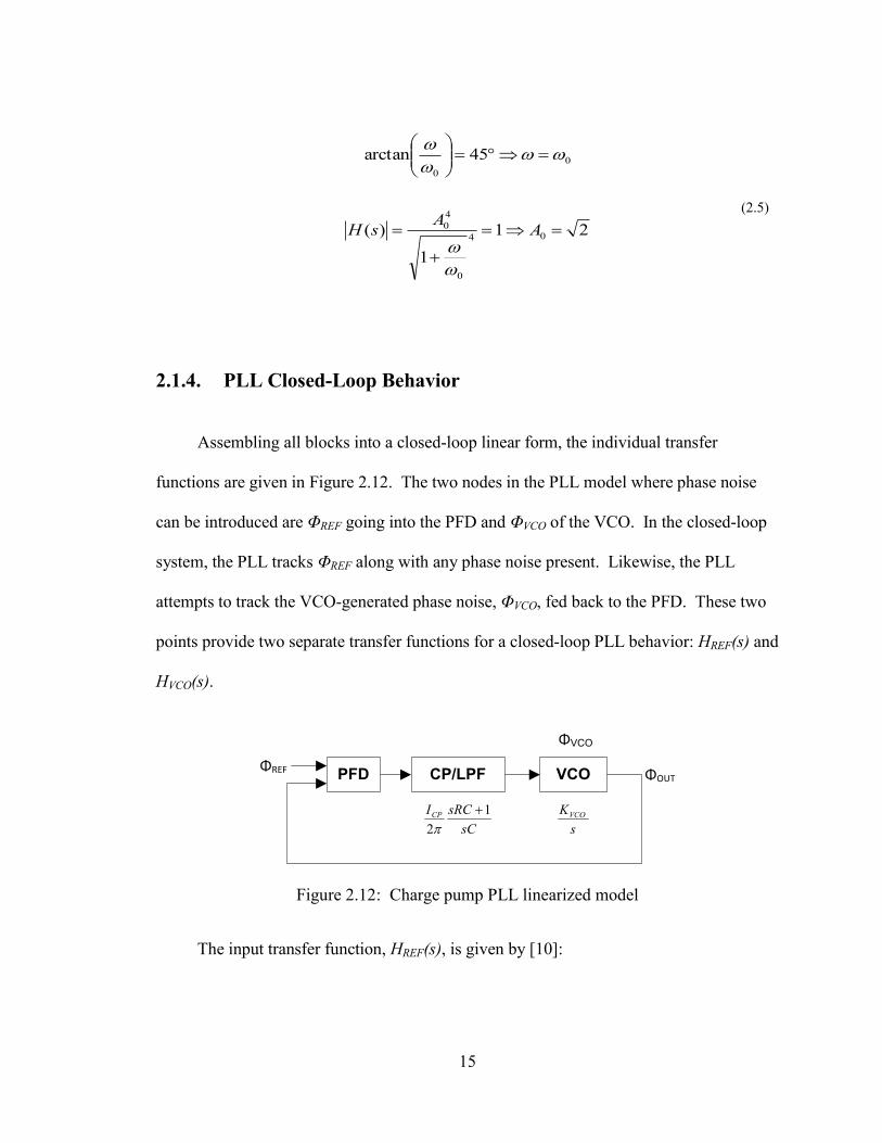
2.1.4. PLL Closed-Loop Behavior .......................................................................... 15
2.1.5. PLL Simulink Model Design and Results .................................................... 17
2.2. Phase Interpolator CDR ....................................................................................... 23
2.2.1. PI Control Loop ............................................................................................ 24
2.2.2. Analog Phase Mixer ...................................................................................... 25
2.2.3. PI CDR Simulink Model ............................................................................... 28
2.3. ΔΣ Modulator ...................................................................................................... 32
2.3.1. Data Converter Overview ............................................................................. 33
2.3.2. Noise Reduction of Oversampling and ΔΣ Modulation ............................... 34
2.3.3. ΔΣ Modulator Loop Filter ............................................................................. 37
2.3.4. ΔΣ Simulink Model....................................................................................... 38
Chapter 3. Techniques for CDR Jitter Reduction ................................................... 43
3.1. Nested Phase Interpolation .................................................................................. 43
vii
3.2. Averaging Phase Interpolation ............................................................................ 45
3.2.1. Simulink Modeled Results ............................................................................ 46
3.3. ΔΣ Averaging Phase Interpolation ...................................................................... 49
3.3.1. Second Order Error-Feedback ΔΣ Modulator............................................... 50
3.3.2. Simulink Modeled Error-Feedback ΔΣ Results ............................................ 52
3.3.3. Simulink Modeled Top-level Results ........................................................... 54
Chapter 4. Lock Detection ......................................................................................... 56
4.1. Techniques Related to CDR Lock Detection ...................................................... 56
4.1.1. Control Voltage Thresholds .......................................................................... 57
4.1.2. Tri-state Phase Detectors .............................................................................. 57
4.2. Proposed Lock Detection ..................................................................................... 58
4.2.1. Lock Detection PI Design ............................................................................. 58
4.2.2. Lock Detection PI Results ............................................................................ 62
Chapter 5. Conclusions............................................................................................... 68
References ........................................................................................................................ 69

viii
LIST OF FIGURES
Figure 1.1 : Example of a source-synchronously clocked high speed link ........................ 2
Figure 1.2 : Example of an eye diagram ............................................................................ 3
Figure 1.3 : Standard phase interpolator CDR ................................................................... 3
Figure 1.4 : Effect of systematic jitter on data eye ............................................................ 4
Figure 2.1 : Generalized charge pump PLL ....................................................................... 6
Figure 2.2 : Input-output behavior of XOR detector ......................................................... 7
Figure 2.3 : Basic linear PFD ............................................................................................. 8
Figure 2.4 : Timing diagram of a linear PFD..................................................................... 9
Figure 2.5 : Input-output characteristics of a linear detector ............................................. 9
Figure 2.6 : Alexander phase detector ............................................................................. 10
Figure 2.7 : Sample points for Alexander PD .................................................................. 11
Figure 2.8 : Alexander PD truth table .............................................................................. 11
Figure 2.9 : Typical charge pump block .......................................................................... 12
Figure 2.10 : Loop filter with smoothing capacitor C2 .................................................... 13
Figure 2.11 : Typical 4-stage ring oscillator .................................................................... 14
Figure 2.12 : Charge pump PLL linearized model .......................................................... 15
Figure 2.13 : Simulink model of a PLL ........................................................................... 18
Figure 2.14 : Simulink model for the VCO and REF CLK ............................................. 18
Figure 2.15 : Simulink linear PFD behavior .................................................................... 19
Figure 2.16 : VCTRL plots for tracking a phase step .......................................................... 20
Figure 2.17 : VCTRL plots for tracking a frequency step ................................................... 21
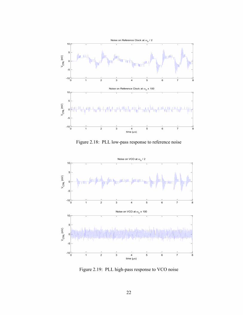
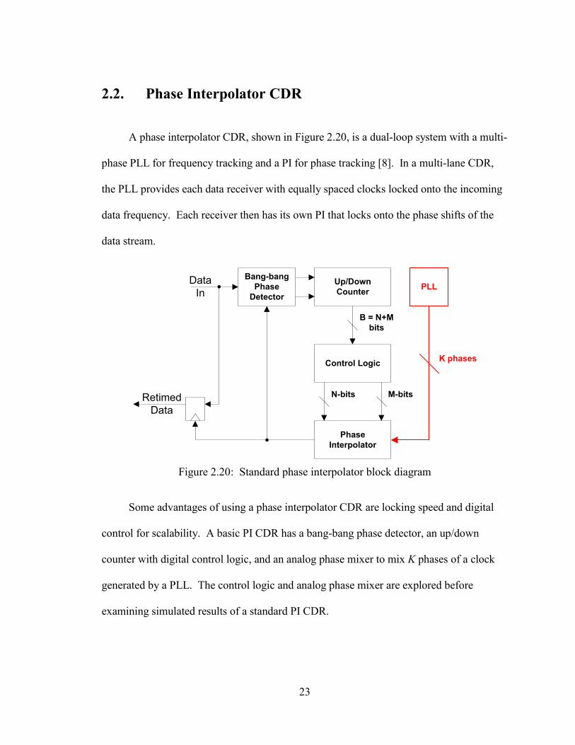
Figure 2.18 : PLL low-pass response to reference noise ................................................. 22
Figure 2.19 : PLL high-pass response to VCO noise....................................................... 22
Figure 2.20 : Standard phase interpolator block diagram ................................................ 23

ix
Figure 2.21 : PI mux selection and α control ................................................................... 24
Figure 2.22 : PI analog phase mixer ................................................................................ 26
Figure 2.23 : Example of poor layout matching of unit current devices ......................... 27
Figure 2.24 : Simulink model for a PI CDR .................................................................... 28
Figure 2.25 : Simulink bang-bang PD behavior .............................................................. 29
Figure 2.26 : Simulink model for the up-down counter................................................... 29
Figure 2.27 : Simulink model for the analog phase mixer ............................................... 30
Figure 2.28 : PI CDR tracking a data stream late by a phase of π ................................... 31
Figure 2.29 : PI CDR tracking a data stream early by a phase of π ................................. 32
Figure 2.30 : Example ADC behavior ............................................................................. 33
Figure 2.31 : Quantization noise spectrum versus signal bandwidth ............................... 34
Figure 2.32 : ΔΣ quantization noise spectrum versus signal bandwidth.......................... 35
Figure 2.33 : ΔΣ in-band quantization noise versus OSR for different orders ................. 36
Figure 2.34 : Standard linearized model for second order ΔΣ modulation ...................... 37
Figure 2.35 : Simulink model for a 1-bit second order ΔΣ modulator ............................ 39
Figure 2.36 : 1-bit quantized second order ΔΣ modulator transient results ..................... 40
Figure 2.37 : 1-bit quantized second order ΔΣ modulator output power spectrum ......... 42
Figure 3.1 : Nested PI block diagram .............................................................................. 44
Figure 3.2 : Averaging phase interpolator block diagram ............................................... 45
Figure 3.3 : Simulink model of averaging phase interpolator ......................................... 47
Figure 3.4 : Simulink model of the phase averaging FSM control .................................. 47
Figure 3.5 : Simulink model of the CDR loop ................................................................. 48
Figure 3.6 : CDR digital control word and PLL VCTRL during a track and lock .............. 48
Figure 3.7 : ΔΣ averaging phase interpolator block diagram........................................... 49
Figure 3.8 : Second order error feedback architecture ..................................................... 51
Figure 3.9 : Tri-level ΔΣ modulator transient response at DC input = 87 (min) ............. 52

x
Figure 3.10 : Tri-level ΔΣ modulator transient response at DC input = 170 (mid) ......... 53
Figure 3.11 : Tri-level ΔΣ modulator transient response at DC input = 255 (max) ........ 53
Figure 3.12 : 32-bit majority voted phase detector behavior ........................................... 54
Figure 3.13 : Top-level locking results ............................................................................ 55
Figure 4.1 : Lock detect PI logic flowchart ..................................................................... 59
Figure 4.2 : Lock detector block diagram ........................................................................ 60
Figure 4.3 : Proposed lock detection PI block diagram ................................................... 61
Figure 4.4 : Jitter tolerance reduction .............................................................................. 61
Figure 4.5 : Simulink model for the proposed lock detection PI CDR ............................ 62
Figure 4.6 : Simulink model for the up-down counter ..................................................... 63
Figure 4.7 : Simulink model for the lock detector ........................................................... 63
Figure 4.8 : Simulink model for the dual phase mixers ................................................... 64
Figure 4.9 : PI counter with no input jitter, lock detection disabled ................................ 65
Figure 4.10 : PI counter with no input jitter, lock detection T=2, L=50 .......................... 66
Figure 4.11 : Eye diagrams for various lock detect setups .............................................. 67
1
Chapter 1. Introduction
Advancements in technology tend to aim at accomplishing more tasks as quickly as
possible. In 2012, Cisco estimated an average 885 petabytes per month of global mobile
data traffic consisting of laptops, tablets, smartphones, and machine-to-machine devices;
an average monthly usage of 11.2 exabytes is projected for 2017 [1]. The number of
online domains increased from 19.8 million in 1997 to 908 million in 2012 [2]. As data
transferring grows in both quantity and speed, hardware is also advancing.
As computer processors with upwards of 12 cores approached 3.4 GHz clock speeds
in recent years, the amount of on-chip data sent to peripheral components demanded for
faster chip-to-chip communication [3]. Many important technologies, such as
smartphones, computers, and high definition televisions, rely on high speed random access
memory (RAM). The JEDEC standard for the still in-development DDR4 is specified for
2.133-4.266 GT/s per lane [4]. As data transfers become increasingly bottlenecked by
communication links, effort is spent on increasing efficiency and minimizing error.
The high-speed link for source-synchronous clocks with multiple data channels,
shown in Figure 1.1 [5], is used in technologies such as RAM, graphics card RAM
(GDDR), and backplane servers [6]. On the receiving side, a clock and data recovery
(CDR) circuit resynchronizes the data with the accompanying clock.

2
CLK TXCLK
Data TX 1Data
Data TX 2
Data TX N
PLL
CDR
CDR
CDR
Transmitter ReceiverChannel
Data
Data
Data
Data
Data
Figure 1.1: Example of a source-synchronously clocked high speed link
1.1. Clock and Data Recovery
In order to minimize error, the receiver must be able to align the clock to the optimal
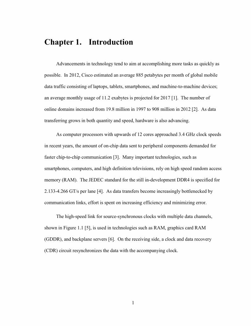
sampling point on the data stream. Ideally, the clock should align with the largest opening
in the data eye diagram, shown in Figure 1.2 [7]. An eye diagram, generated by
overlaying all data transitions within a single frame, allows designers to see effects of
jitter and timing mismatch. This realignment is the function of a CDR.
There are many CDR architectures including phase-locked loops (PLL), delay-locked
loops (DLL), or phase interpolators (PI) [5]. Each architecture has its strengths and
limitations, but due to the nature of multi-lane data transfer with source-sychronized
clocking, this work focused on the PI architecture [8].
3
Figure 1.2: Example of an eye diagram
1.1.1. Phase Interpolator
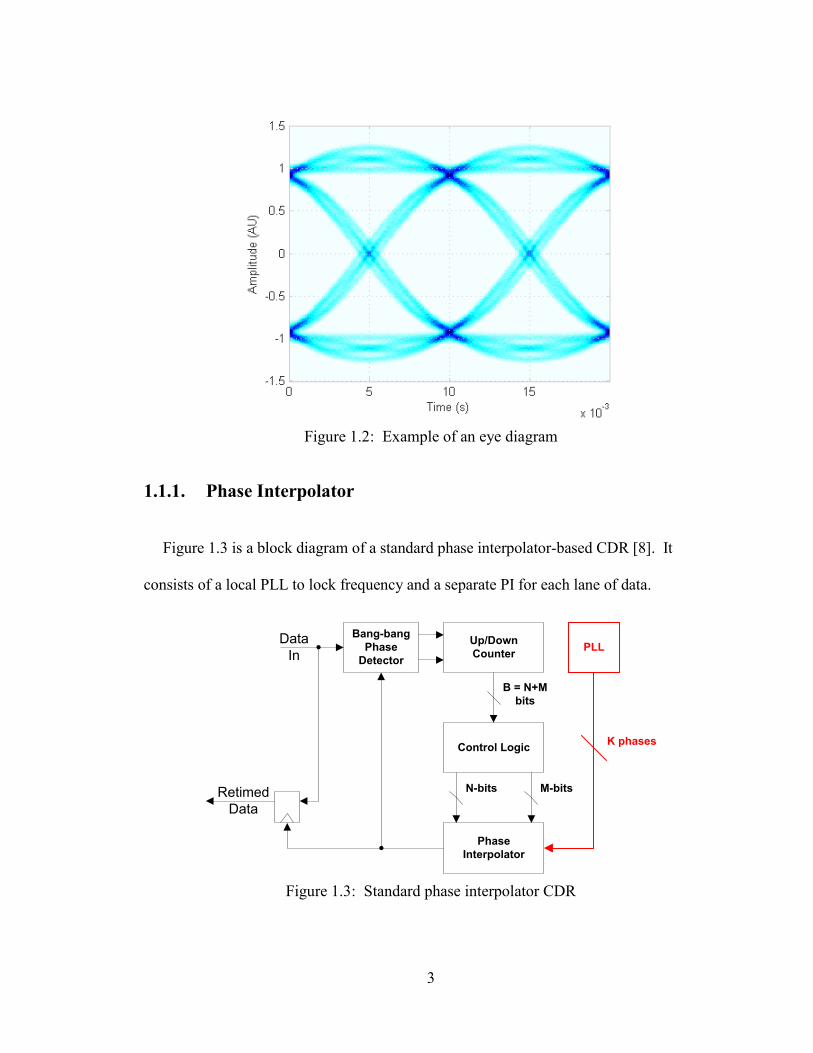
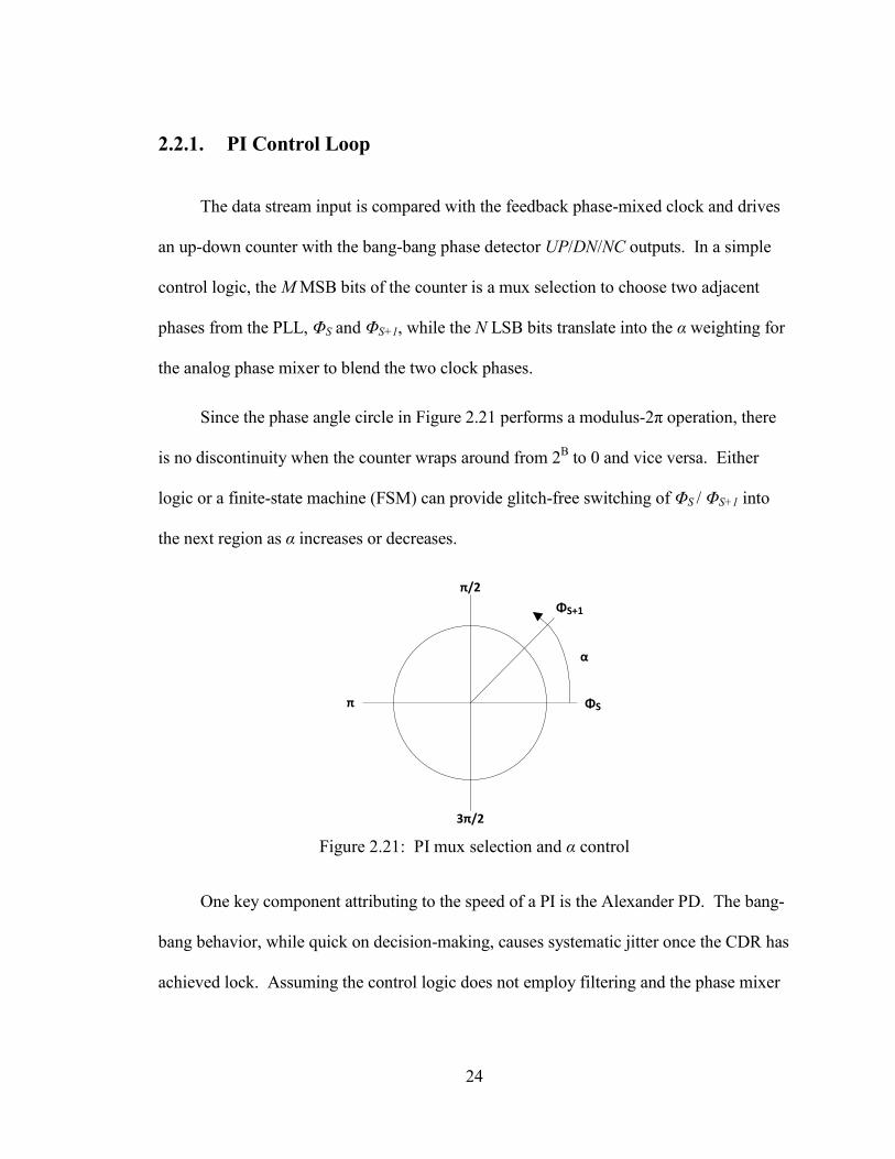
Figure 1.3 is a block diagram of a standard phase interpolator-based CDR [8]. It
consists of a local PLL to lock frequency and a separate PI for each lane of data.
B = N+M
bits
M-bits
Bang-bang
Phase
Detector
Up/Down
Counter
Control Logic
Phase
Interpolator
PLL
K phases
N-bitsRetimed
Data
Data
In
Figure 1.3: Standard phase interpolator CDR
4
This is a dual-loop architecture, separating the tasks of frequency tracking and high-
speed phase tracking. The primary control loop is digital, allowing it accuracy, speed, and
portability across processes. The bang-bang phase detector (!!PD) detects whether the
recovered clock is ahead or behind the data stream in a binary fashion [9], giving the PI a
very quick phase tracking.
1.1.2. Systematic Jitter
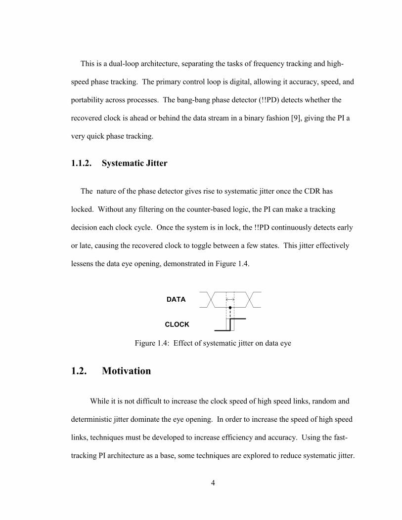
The nature of the phase detector gives rise to systematic jitter once the CDR has
locked. Without any filtering on the counter-based logic, the PI can make a tracking
decision each clock cycle. Once the system is in lock, the !!PD continuously detects early
or late, causing the recovered clock to toggle between a few states. This jitter effectively
lessens the data eye opening, demonstrated in Figure 1.4.
DATA
CLOCK
Figure 1.4: Effect of systematic jitter on data eye
1.2. Motivation
While it is not difficult to increase the clock speed of high speed links, random and
deterministic jitter dominate the eye opening. In order to increase the speed of high speed
links, techniques must be developed to increase efficiency and accuracy. Using the fast-
tracking PI architecture as a base, some techniques are explored to reduce systematic jitter.
5
The first utilizes a ΔΣ modulator in an attempt to shape and filter the noise power and the
second technique compromises jitter tolerance in order to eliminate the in-lock jitter.
1.3. Organization
Chapter 2 reviews background information on various CDR building blocks for the
PLL-PI dual loop architecture. Each building block of the CDR is examined for points of
improvement. The concept and stability of ΔΣ modulation, applications of ΔΣ, and
limitations are also explored. Chapter 3 introduces several existing techniques for
reducing systematic jitter in CDR. Finally, Chapter 4 presents a novel lock detection PI
architecture that eliminates systematic jitter.
6
Chapter 2. Background
Clock and data recovery circuits have many available topologies, but the heart of all
CDR operations lie within the phase-tracking mechanism. Simple single-loop
architectures feature a PLL for frequency and phase tracking while dual-loop architectures
track frequency and phase separately [5]. This chapter details the functionality of a PLL
and explores the dual-loop PLL-PI CDR architecture.
2.1. Phase-Locked Loops
A PLL is a negative feedback system that continuously adjusts a voltage-controlled
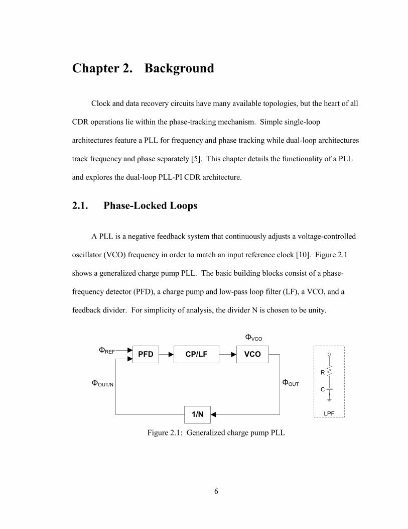
oscillator (VCO) frequency in order to match an input reference clock [10]. Figure 2.1
shows a generalized charge pump PLL. The basic building blocks consist of a phase-
frequency detector (PFD), a charge pump and low-pass loop filter (LF), a VCO, and a
feedback divider. For simplicity of analysis, the divider N is chosen to be unity.
PFD CP/LF VCO
1/N
ΦVCO
ΦOUTΦOUT/N
ΦREF
LPF
R
C
Figure 2.1: Generalized charge pump PLL

7
The phase detector takes in a reference clock and compares that to the feedback
clock from the VCO to generate an “early” (DN signal) or “late” (UP signal) output. The
charge pump and loop filter takes the UP and DN signals and raises or lowers the control
voltage, respectively. Finally, this control voltage adjusts the VCO output clock
frequency. Once the system is in a closed loop, the VCO continuously adjusts itself to
remain locked to the reference.
2.1.1. Phase-Frequency Detector
The PFD compares two input clocks and generates an output signifying which
signal is faster or slower [10]. The output of the PFD is filtered into a control signal to
provide a negative feedback for the VCO. A very simplistic detector can be implemented
with an XOR gate. The output is high in proportion to the duration that the signals are
mismatched, demonstrated in Figure 2.2.
A
B
XOR
Figure 2.2: Input-output behavior of XOR detector
However, the XOR implementation does not distinguish between rising or falling
clock edges. This type of detector can only produce a pulse proportional to the phase
8
difference in two clock edges. For a PLL, the PFD has to be able to distinguish “early”
from “late.” These detectors are split into two main types: linear and binary.
2.1.1.1. Linear Detector
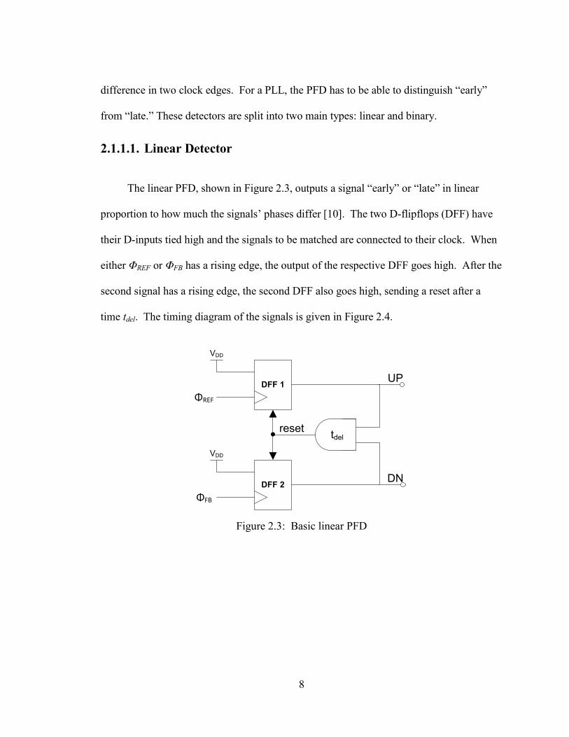
The linear PFD, shown in Figure 2.3, outputs a signal “early” or “late” in linear
proportion to how much the signals’ phases differ [10]. The two D-flipflops (DFF) have
their D-inputs tied high and the signals to be matched are connected to their clock. When
either ΦREF or ΦFB has a rising edge, the output of the respective DFF goes high. After the
second signal has a rising edge, the second DFF also goes high, sending a reset after a
time tdel. The timing diagram of the signals is given in Figure 2.4.
UP
DN
resettdel
DFF 1
DFF 2
ΦREF
ΦFB
VDD
VDD
Figure 2.3: Basic linear PFD
9
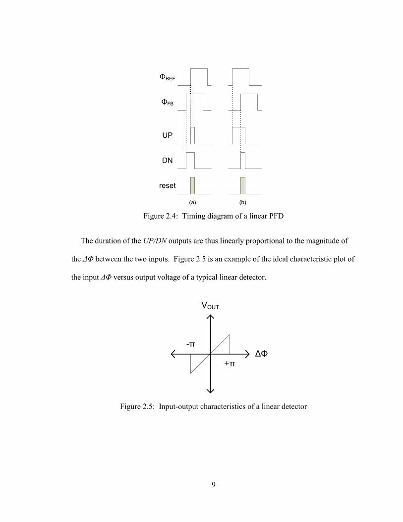
ΦREF
ΦFB
UP
DN
reset
(a) (b)
Figure 2.4: Timing diagram of a linear PFD
The duration of the UP/DN outputs are thus linearly proportional to the magnitude of
the ΔΦ between the two inputs. Figure 2.5 is an example of the ideal characteristic plot of
the input ΔΦ versus output voltage of a typical linear detector.
ΔΦ
VOUT
+π
-π
Figure 2.5: Input-output characteristics of a linear detector
10
2.1.1.2. Binary Detector
While the linear detector requires analog components (charge pump and analog loop
filter) to create a final control voltage, the binary detector simply outputs a digital code for
UP or DN given a positive or negative ΔΦ. True to the name, this detector has two
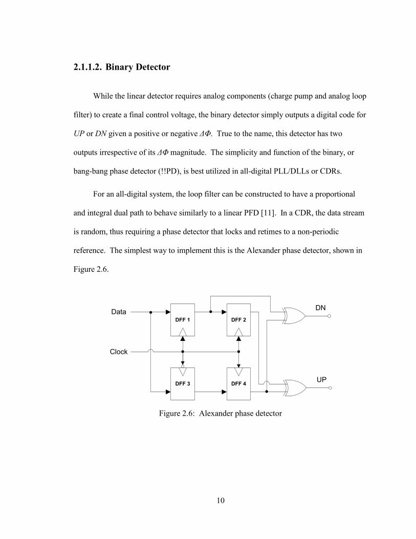
outputs irrespective of its ΔΦ magnitude. The simplicity and function of the binary, or
bang-bang phase detector (!!PD), is best utilized in all-digital PLL/DLLs or CDRs.
For an all-digital system, the loop filter can be constructed to have a proportional
and integral dual path to behave similarly to a linear PFD [11]. In a CDR, the data stream
is random, thus requiring a phase detector that locks and retimes to a non-periodic
reference. The simplest way to implement this is the Alexander phase detector, shown in
Figure 2.6.
DFF 1
DFF 3
DFF 2
DFF 4
Clock
DataDN
UP
Figure 2.6: Alexander phase detector
11
A B C
DATA
CLOCK
A B C
Clock
Early
Clock
Late
Figure 2.7: Sample points for Alexander PD
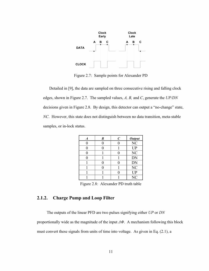
Detailed in [9], the data are sampled on three consecutive rising and falling clock
edges, shown in Figure 2.7. The sampled values, A, B, and C, generate the UP/DN
decisions given in Figure 2.8. By design, this detector can output a “no-change” state,
NC. However, this state does not distinguish between no data transition, meta-stable
samples, or in-lock status.
A B C Output
0 0 0 NC
0 0 1 UP
0 1 0 NC
0 1 1 DN
1 0 0 DN
1 0 1 NC
1 1 0 UP
1 1 1 NC
Figure 2.8: Alexander PD truth table
2.1.2. Charge Pump and Loop Filter
The outputs of the linear PFD are two pulses signifying either UP or DN
proportionally wide as the magnitude of the input ΔΦ. A mechanism following this block
must convert these signals from units of time into voltage. As given in Eq. (2.1), a
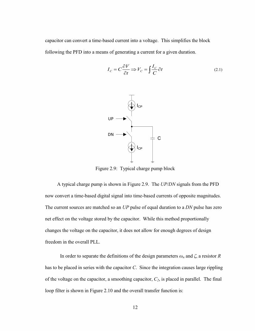
12
capacitor can convert a time-based current into a voltage. This simplifies the block
following the PFD into a means of generating a current for a given duration.
t
C
IV
t
VCI C
CC (2.1)
C
ICP
ICP
UP
DN
Figure 2.9: Typical charge pump block
A typical charge pump is shown in Figure 2.9. The UP/DN signals from the PFD
now convert a time-based digital signal into time-based currents of opposite magnitudes.
The current sources are matched so an UP pulse of equal duration to a DN pulse has zero
net effect on the voltage stored by the capacitor. While this method proportionally
changes the voltage on the capacitor, it does not allow for enough degrees of design
freedom in the overall PLL.
In order to separate the definitions of the design parameters ωn and ζ, a resistor R
has to be placed in series with the capacitor C. Since the integration causes large rippling
of the voltage on the capacitor, a smoothing capacitor, C2, is placed in parallel. The final
loop filter is shown in Figure 2.10 and the overall transfer function is:
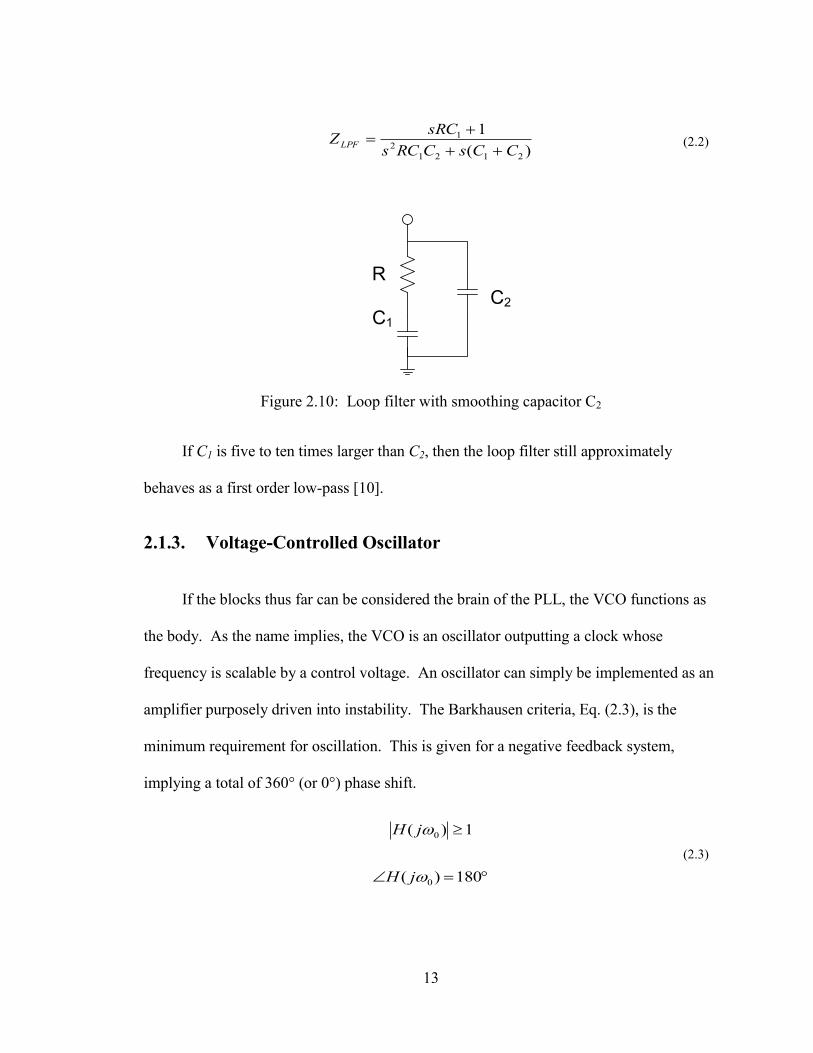
13
)(
1
2121
2
1
CCsCRCs
sRCZLPF
(2.2)
C2
R
C1
Figure 2.10: Loop filter with smoothing capacitor C2
If C1 is five to ten times larger than C2, then the loop filter still approximately
behaves as a first order low-pass [10].
2.1.3. Voltage-Controlled Oscillator
If the blocks thus far can be considered the brain of the PLL, the VCO functions as
the body. As the name implies, the VCO is an oscillator outputting a clock whose
frequency is scalable by a control voltage. An oscillator can simply be implemented as an
amplifier purposely driven into instability. The Barkhausen criteria, Eq. (2.3), is the
minimum requirement for oscillation. This is given for a negative feedback system,
implying a total of 360° (or 0°) phase shift.
1)( 0 jH
180)( 0jH
(2.3)
14
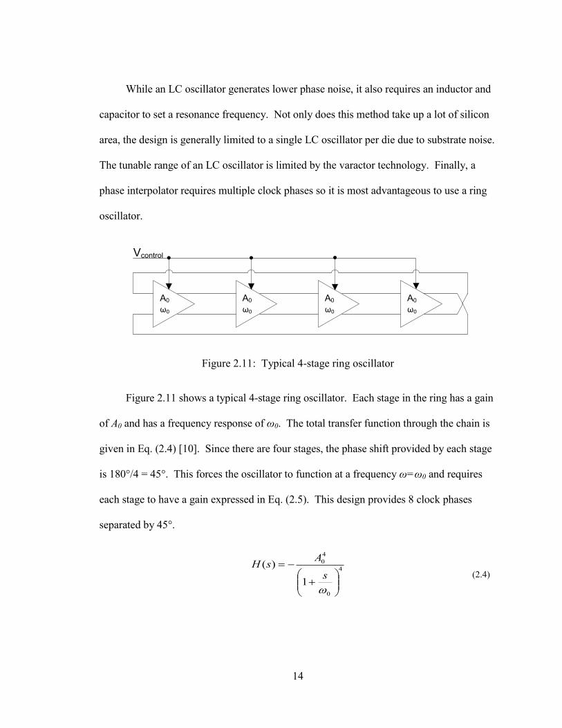
While an LC oscillator generates lower phase noise, it also requires an inductor and
capacitor to set a resonance frequency. Not only does this method take up a lot of silicon
area, the design is generally limited to a single LC oscillator per die due to substrate noise.
The tunable range of an LC oscillator is limited by the varactor technology. Finally, a
phase interpolator requires multiple clock phases so it is most advantageous to use a ring
oscillator.
Vcontrol
A0
ω0
A0
ω0
A0
ω0
A0
ω0
Figure 2.11: Typical 4-stage ring oscillator
Figure 2.11 shows a typical 4-stage ring oscillator. Each stage in the ring has a gain
of A0 and has a frequency response of ω0. The total transfer function through the chain is
given in Eq. (2.4) [10]. Since there are four stages, the phase shift provided by each stage
is 180°/4 = 45°. This forces the oscillator to function at a frequency ω=ω0 and requires
each stage to have a gain expressed in Eq. (2.5). This design provides 8 clock phases
separated by 45°.
4
0
4
0
1
)(
s
AsH
(2.4)
15
0
0
45arctan
21
1
)( 04
0
4
0
AA
sH
(2.5)
2.1.4. PLL Closed-Loop Behavior
Assembling all blocks into a closed-loop linear form, the individual transfer
functions are given in Figure 2.12. The two nodes in the PLL model where phase noise
can be introduced are ΦREF going into the PFD and ΦVCO of the VCO. In the closed-loop
system, the PLL tracks ΦREF along with any phase noise present. Likewise, the PLL
attempts to track the VCO-generated phase noise, ΦVCO, fed back to the PFD. These two
points provide two separate transfer functions for a closed-loop PLL behavior: HREF(s) and
HVCO(s).
PFD CP/LPF VCO
ΦVCO
ΦOUTΦREF
sC
sRCICP 1
2
s
KVCO
Figure 2.12: Charge pump PLL linearized model
The input transfer function, HREF(s), is given by [10]:

16
C
IKs
RIKs
sRCC
KI
sHCPVCOCPVCO
VCOCP
REF
OUTREF
22
)1(2)(
2
(2.6)
Comparing the HREF(s) with a second-order transfer function from basic control
theory, Eq. (2.7), yields the parameters in Eq. (2.8).
22
2
2
2)(
nn
nnREF
ss
ssH
(2.7)
C
KIRC
C
KI VCOCPVCOCPn
22,
2 (2.8)
Using the same parameters, the VCO transfer function, HVCO(s), is given by:
22
2
2)(
nn
VCOss
ssH
(2.9)
These transfer functions indicate that phase noise on ΦREF has a low-pass response
through the PLL while the noise on ΦVCO has a high-pass response.
The parameter ωn represents the PLL’s natural frequency and ζ is the damping
factor. These two loop parameters determine the PLL stability and give a starting point to
calculate device sizes. For closed-loop stability, the PLL natural frequency should be
approximately 10-20 times lower than the input reference [12]. For maximal loop
response time with minimized transient ringing, ζ should be set as 0.707 for a critically
damped system. For fine-tuning the system for stability, the loop filter capacitors, C1 and
C2, can influence the phase margin:
17
1,
2
1tan
2
11
C
Cb
b
bPM (2.10)
Finally, the settling time of the PLL can be adjusted with the approximation:
n
settleT
6.4 (2.11)
With these basic guidelines as a starting point, all remaining PLL parameters can be
calculated based on the design of the PFD, charge pump, loop filter, and VCO.
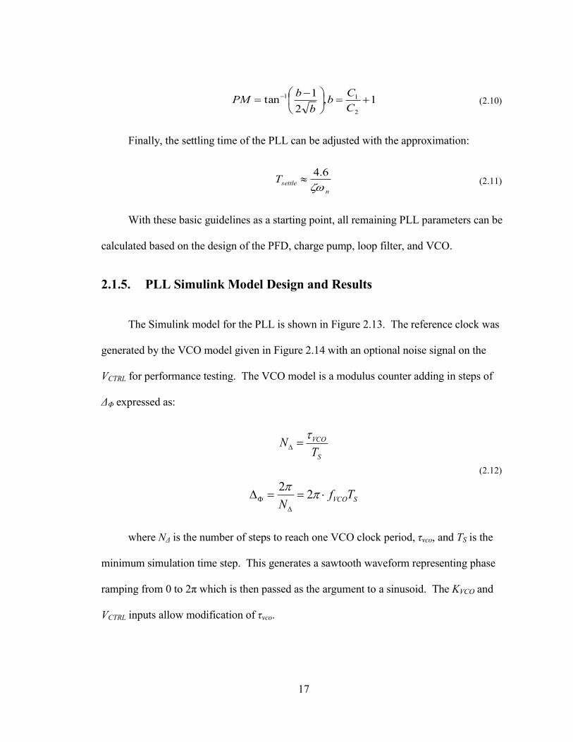
2.1.5. PLL Simulink Model Design and Results
The Simulink model for the PLL is shown in Figure 2.13. The reference clock was
generated by the VCO model given in Figure 2.14 with an optional noise signal on the
VCTRL for performance testing. The VCO model is a modulus counter adding in steps of
ΔΦ expressed as:
S
VCO
TN
SVCOTfN
22
(2.12)
where NΔ is the number of steps to reach one VCO clock period, τvco, and TS is the
minimum simulation time step. This generates a sawtooth waveform representing phase
ramping from 0 to 2π which is then passed as the argument to a sinusoid. The KVCO and
VCTRL inputs allow modification of τvco.
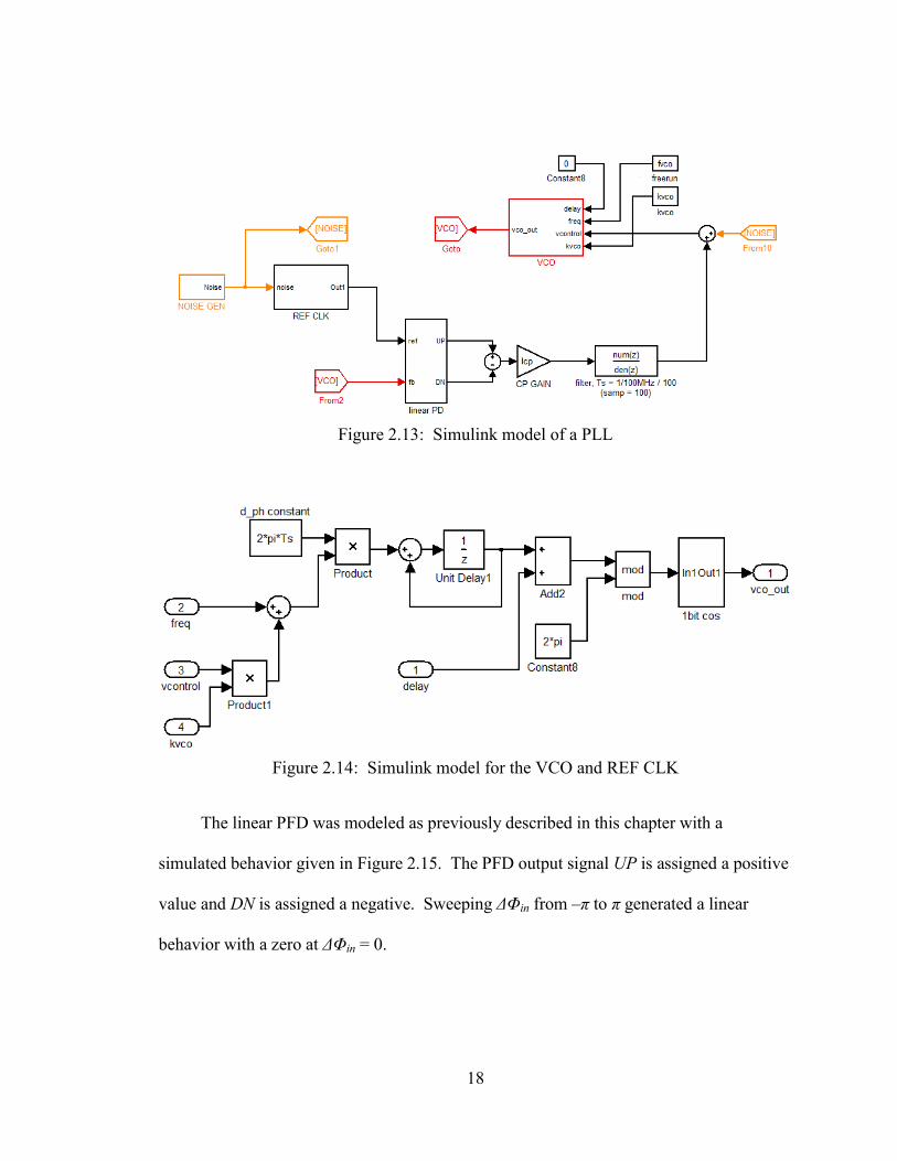
18
Figure 2.13: Simulink model of a PLL
Figure 2.14: Simulink model for the VCO and REF CLK
The linear PFD was modeled as previously described in this chapter with a
simulated behavior given in Figure 2.15. The PFD output signal UP is assigned a positive
value and DN is assigned a negative. Sweeping ΔΦin from –π to π generated a linear
behavior with a zero at ΔΦin = 0.

19
Figure 2.15: Simulink linear PFD behavior
Design began by arbitrarily choosing a reference frequency of 100 MHz, implying
an initial ωn of 5 MHz. Having a ring oscillator design with KVCO = 400 MHz/V gives a
tuning range of ±50 MHz using only 0.3 V. An initial loop filter capacitor was estimated
to be 50-100 times larger than potential parasitic capacitances on the node. Since the loop
filter node is connected to the VCO control gates and the drains of the charge pump, an
initial estimation of 50 pF was chosen. For a critically damped loop response, damping
factor ζ needs to be 0.707. Now Eq. (2.8) becomes a system of two variables, ICP and R.
Solving this system of equations yielded 30 μA for ICP and 2.2 kΩ for R.
The VCTRL smoothing capacitor was empirically chosen by running a simulated
sweep starting at C1 /10 and reducing C2 until ripples appeared on VCTRL. A final sizing of
-3 -2 -1 0 1 2 3
-1
-0.8
-0.6
-0.4
-0.2
0
0.2
0.4
0.6
0.8
1
Linear PFD Behavior
in
(radians)
Norm
aliz
ed C
ontr
ol V
oltage (
V)

20
C2 was chosen to be C1 /25 to offer ripple reduction while still offering a phase margin of
67.8° given by Eq. (2.10).
With the calculated parameters, the PLL was simulated in a closed loop and tracks a
static reference clock. After a time, the reference clock was given a step in phase and
Figure 2.16 shows the VCTRL keeping the lock. Similarly, Figure 2.17 exhibits the VCTRL
tracking the reference clock after a frequency step. Based on Eq. (2.11), the calculated
settling time was approximately 0.523 μs. This estimation is fairly accurate as the step
responses all settle within 0.45 μs.
Figure 2.16: VCTRL plots for tracking a phase step
9.9 10 10.1 10.2 10.3 10.4 10.5-30
-20
-10
0
VC
TR
L (
mV
)
VCTRL
tracking + on Reference Clock
9.9 10 10.1 10.2 10.3 10.4 10.5-10
0
10
20
30
time (s)
VC
TR
L (
mV
)
VCTRL
tracking - on Reference Clock
21
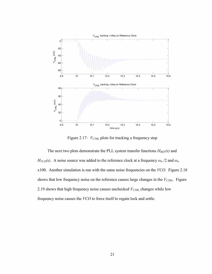
Figure 2.17: VCTRL plots for tracking a frequency step
The next two plots demonstrate the PLL system transfer functions HREF(s) and
HVCO(s). A noise source was added to the reference clock at a frequency ωn /2 and ωn
x100. Another simulation is run with the same noise frequencies on the VCO. Figure 2.18
shows that low frequency noise on the reference causes large changes in the VCTRL. Figure
2.19 shows that high frequency noise causes unchecked VCTRL changes while low
frequency noise causes the VCO to force itself to regain lock and settle.
9.9 10 10.1 10.2 10.3 10.4 10.5 10.6
-80
-60
-40
-20
0
VC
TR
L (
mV
)
VCTRL
tracking +freq on Reference Clock
9.9 10 10.1 10.2 10.3 10.4 10.5 10.6
0
20
40
60
80
time (s)
VC
TR
L (
mV
)
VCTRL
tracking -freq on Reference Clock
22
Figure 2.18: PLL low-pass response to reference noise
Figure 2.19: PLL high-pass response to VCO noise
0 1 2 3 4 5 6 7 8-10
-5
0
5
10
VC
TRL (
mV
)
Noise on Reference Clock at n / 2
0 1 2 3 4 5 6 7 8-10
-5
0
5
10
time (s)
VC
TR
L (
mV
)
Noise on Reference Clock at n x 100
0 1 2 3 4 5 6 7 8-10
-5
0
5
10
VC
TR
L (
mV
)
Noise on VCO at n / 2
0 1 2 3 4 5 6 7 8-10
-5
0
5
10
time (s)
VC
TR
L (
mV
)
Noise on VCO at n x 100
23
2.2. Phase Interpolator CDR
A phase interpolator CDR, shown in Figure 2.20, is a dual-loop system with a multi-
phase PLL for frequency tracking and a PI for phase tracking [8]. In a multi-lane CDR,
the PLL provides each data receiver with equally spaced clocks locked onto the incoming
data frequency. Each receiver then has its own PI that locks onto the phase shifts of the
data stream.
B = N+M
bits
M-bits
Bang-bang
Phase
Detector
Up/Down
Counter
Control Logic
Phase
Interpolator
PLL
K phases
N-bitsRetimed
Data
Data
In
Figure 2.20: Standard phase interpolator block diagram
Some advantages of using a phase interpolator CDR are locking speed and digital
control for scalability. A basic PI CDR has a bang-bang phase detector, an up/down
counter with digital control logic, and an analog phase mixer to mix K phases of a clock
generated by a PLL. The control logic and analog phase mixer are explored before
examining simulated results of a standard PI CDR.
24
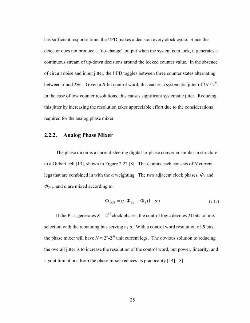
2.2.1. PI Control Loop
The data stream input is compared with the feedback phase-mixed clock and drives
an up-down counter with the bang-bang phase detector UP/DN/NC outputs. In a simple
control logic, the M MSB bits of the counter is a mux selection to choose two adjacent
phases from the PLL, ΦS and ΦS+1, while the N LSB bits translate into the α weighting for
the analog phase mixer to blend the two clock phases.
Since the phase angle circle in Figure 2.21 performs a modulus-2π operation, there
is no discontinuity when the counter wraps around from 2B to 0 and vice versa. Either
logic or a finite-state machine (FSM) can provide glitch-free switching of ΦS / ΦS+1 into
the next region as α increases or decreases.
ΦS+1
α
π
π/2
3π/2
ΦS
Figure 2.21: PI mux selection and α control
One key component attributing to the speed of a PI is the Alexander PD. The bang-
bang behavior, while quick on decision-making, causes systematic jitter once the CDR has
achieved lock. Assuming the control logic does not employ filtering and the phase mixer
25
has sufficient response time, the !!PD makes a decision every clock cycle. Since the
detector does not produce a “no-change” output when the system is in lock, it generates a
continuous stream of up/down decisions around the locked counter value. In the absence
of circuit noise and input jitter, the !!PD toggles between three counter states alternating
between X and X±1. Given a B-bit control word, this causes a systematic jitter of UI / 2B.
In the case of low counter resolutions, this causes significant systematic jitter. Reducing
this jitter by increasing the resolution takes appreciable effort due to the considerations
required for the analog phase mixer.
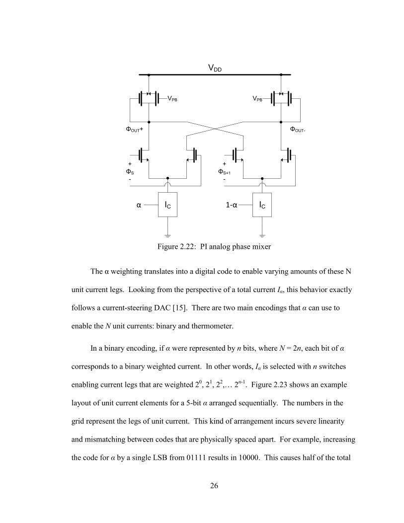
2.2.2. Analog Phase Mixer
The phase mixer is a current-steering digital-to-phase converter similar in structure
to a Gilbert cell [13], shown in Figure 2.22 [8]. The IC units each consists of N current
legs that are combined in with the α weighting. The two adjacent clock phases, ΦS and
ΦS+1, and α are mixed according to:
)1(1 SSOUT (2.13)
If the PLL generates K = 2M
clock phases, the control logic devotes M bits to mux
selection with the remaining bits serving as α. With a control word resolution of B bits,
the phase mixer will have N = 2B-2
M unit current legs. The obvious solution to reducing
the overall jitter is to increase the resolution of the control word, but power, linearity, and
layout limitations from the phase mixer reduces its practicality [14], [8].
26
IC IC
+
ΦS+1
-
+
ΦS
-
α 1-α
VPB VPB
VDD
ΦOUT+ ΦOUT-
Figure 2.22: PI analog phase mixer
The α weighting translates into a digital code to enable varying amounts of these N
unit current legs. Looking from the perspective of a total current Iα, this behavior exactly
follows a current-steering DAC [15]. There are two main encodings that α can use to
enable the N unit currents: binary and thermometer.
In a binary encoding, if α were represented by n bits, where N = 2n, each bit of α
corresponds to a binary weighted current. In other words, Iα is selected with n switches
enabling current legs that are weighted 20, 2
1, 2
2,… 2
n-1. Figure 2.23 shows an example
layout of unit current elements for a 5-bit α arranged sequentially. The numbers in the
grid represent the legs of unit current. This kind of arrangement incurs severe linearity
and mismatching between codes that are physically spaced apart. For example, increasing
the code for α by a single LSB from 01111 results in 10000. This causes half of the total
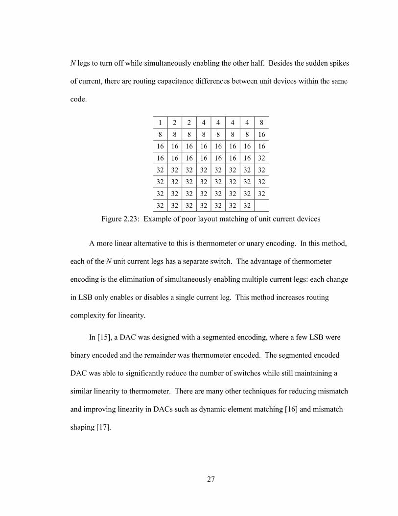
27
N legs to turn off while simultaneously enabling the other half. Besides the sudden spikes
of current, there are routing capacitance differences between unit devices within the same
code.
1 2 2 4 4 4 4 8
8 8 8 8 8 8 8 16
16 16 16 16 16 16 16 16
16 16 16 16 16 16 16 32
32 32 32 32 32 32 32 32
32 32 32 32 32 32 32 32
32 32 32 32 32 32 32 32
32 32 32 32 32 32 32
Figure 2.23: Example of poor layout matching of unit current devices
A more linear alternative to this is thermometer or unary encoding. In this method,
each of the N unit current legs has a separate switch. The advantage of thermometer
encoding is the elimination of simultaneously enabling multiple current legs: each change
in LSB only enables or disables a single current leg. This method increases routing
complexity for linearity.
In [15], a DAC was designed with a segmented encoding, where a few LSB were
binary encoded and the remainder was thermometer encoded. The segmented encoded
DAC was able to significantly reduce the number of switches while still maintaining a
similar linearity to thermometer. There are many other techniques for reducing mismatch
and improving linearity in DACs such as dynamic element matching [16] and mismatch
shaping [17].
28
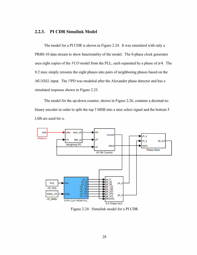
2.2.3. PI CDR Simulink Model
The model for a PI CDR is shown in Figure 2.24. It was simulated with only a
PRBS-10 data stream to show functionality of the model. The 8-phase clock generator
uses eight copies of the VCO model from the PLL, each separated by a phase of π/4. The
8:2 mux simply reroutes the eight phases into pairs of neighboring phases based on the
MUXSEL input. The !!PD was modeled after the Alexander phase detector and has a
simulated response shown in Figure 2.25.
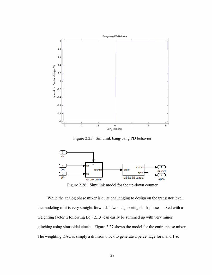
The model for the up-down counter, shown in Figure 2.26, contains a decimal-to-
binary encoder in order to split the top 3 MSB into a mux select signal and the bottom 5
LSB are used for α.
Figure 2.24: Simulink model for a PI CDR
29
Figure 2.25: Simulink bang-bang PD behavior
Figure 2.26: Simulink model for the up-down counter
While the analog phase mixer is quite challenging to design on the transistor level,
the modeling of it is very straight-forward. Two neighboring clock phases mixed with a
weighting factor α following Eq. (2.13) can easily be summed up with very minor
glitching using sinusoidal clocks. Figure 2.27 shows the model for the entire phase mixer.
The weighting DAC is simply a division block to generate a percentage for α and 1-α.
-3 -2 -1 0 1 2 3
-1
-0.8
-0.6
-0.4
-0.2
0
0.2
0.4
0.6
0.8
1
Bang-bang PD Behavior
in
(radians)
Norm
aliz
ed C
ontr
ol V
oltage (
V)
30
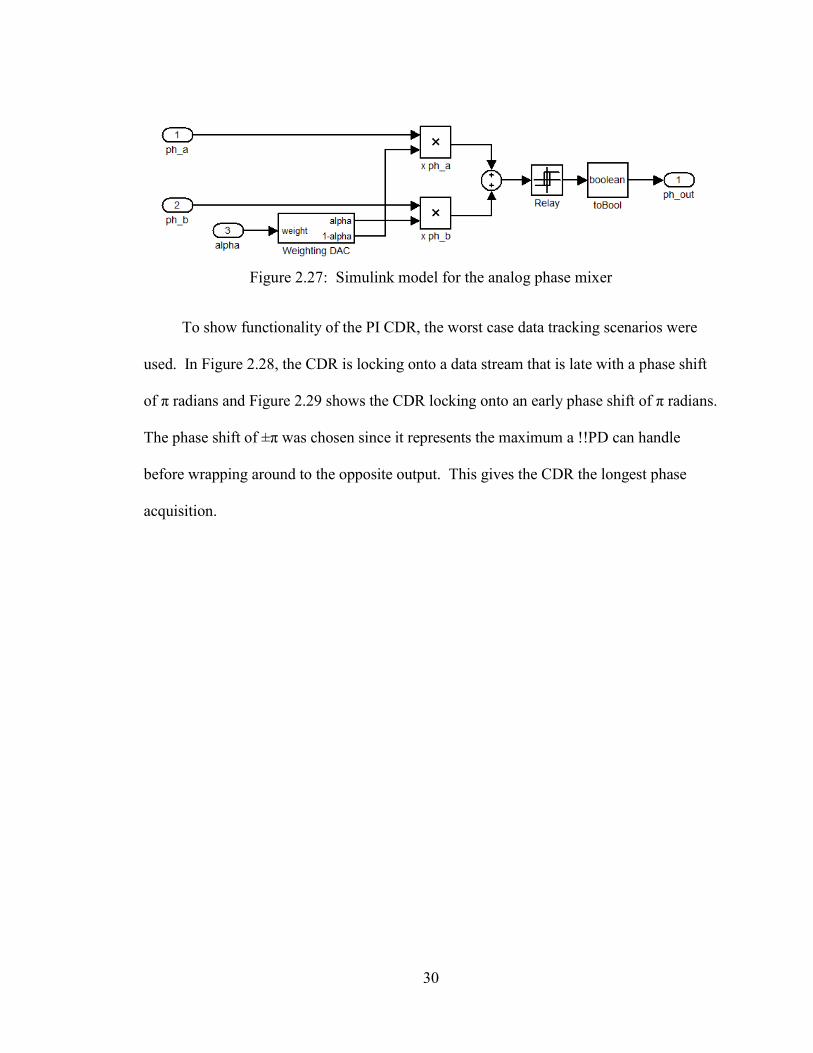
Figure 2.27: Simulink model for the analog phase mixer
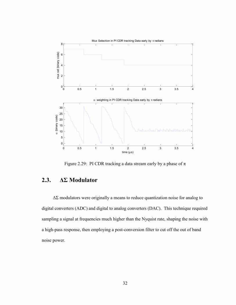
To show functionality of the PI CDR, the worst case data tracking scenarios were
used. In Figure 2.28, the CDR is locking onto a data stream that is late with a phase shift
of π radians and Figure 2.29 shows the CDR locking onto an early phase shift of π radians.
The phase shift of ±π was chosen since it represents the maximum a !!PD can handle
before wrapping around to the opposite output. This gives the CDR the longest phase
acquisition.

31
Figure 2.28: PI CDR tracking a data stream late by a phase of π
0 0.5 1 1.5 2 2.5 3 3.5 4
0
0.5
1
1.5
2
2.5
3
mux s
el (b
inary
code)
Mux Selection in PI CDR tracking Data late by radians
0 0.5 1 1.5 2 2.5 3 3.5 4
0
5
10
15
20
25
30
time (s)
(
bin
ary
code)
weighting in PI CDR tracking Data late by radians
32
Figure 2.29: PI CDR tracking a data stream early by a phase of π
2.3. ΔΣ Modulator
ΔΣ modulators were originally a means to reduce quantization noise for analog to
digital converters (ADC) and digital to analog converters (DAC). This technique required
sampling a signal at frequencies much higher than the Nyquist rate, shaping the noise with
a high-pass response, then employing a post-conversion filter to cut off the out of band
noise power.
0 0.5 1 1.5 2 2.5 3 3.5 40
2
4
6
8
mux s
el (b
inary
code)
Mux Selection in PI CDR tracking Data early by radians
0 0.5 1 1.5 2 2.5 3 3.5 4
0
5
10
15
20
25
30
time (s)
(
bin
ary
code)
weighting in PI CDR tracking Data early by radians

33
2.3.1. Data Converter Overview
Δ 2Δ 3Δ
AIN
DOUT
D1
D2
D3
Figure 2.30: Example ADC behavior
An example of an ADC behavior is shown in Figure 2.30, where AIN represents each
analog voltage and DOUT are the outputted digital codes. A B-bit ADC converts an analog
signal into a digital equivalent with 2B quantized levels [18]. A uniform error occurs at
each level of quantization for each of the 2B codes. Given an ADC input with a max
voltage range of VMAX, each digitized code has an analog voltage step of Δ or VLSB,
expressed as:
B
MAXV
2 (2.14)
Provided a sawtooth input covering the entire ADC range, integrating the
quantization error across one period yields a quantization noise power, εqrms, given by:
12
22 qqrms (2.15)
34
Calculating the theoretical maximum signal to noise ratio (SNR) for a sinusoid input
with peak-to-peak amplitude of VMAX is simplified down to Eq. (2.16), given as signal to
quantization noise ratio (SQNR).
76.102.6 BSQNR (2.16)
With a standard Nyquist-rate converter the sampling bandwidth extends out to twice
the maximum signal bandwidth. An oversampled converter can utilize higher sampling
frequencies in exchange for lowering the in-band quantization noise.
2.3.2. Noise Reduction of Oversampling and ΔΣ Modulation
No
ise
po
we
r
fBW fS/2
12
2
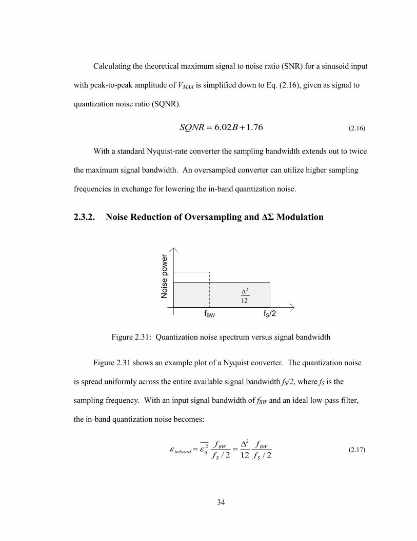
Figure 2.31: Quantization noise spectrum versus signal bandwidth
Figure 2.31 shows an example plot of a Nyquist converter. The quantization noise
is spread uniformly across the entire available signal bandwidth fS/2, where fS is the
sampling frequency. With an input signal bandwidth of fBW and an ideal low-pass filter,
the in-band quantization noise becomes:
2/122/
22
S
BW
S
BWqinband
f
f
f
f (2.17)
35
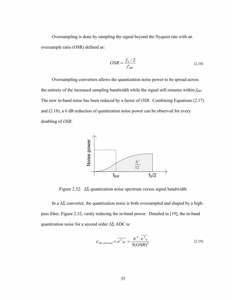
Oversampling is done by sampling the signal beyond the Nyquist rate with an
oversample ratio (OSR) defined as:
BW
S
f
fOSR
2/ (2.18)
Oversampling converters allows the quantization noise power to be spread across
the entirety of the increased sampling bandwidth while the signal still remains within fBW.
The new in-band noise has been reduced by a factor of OSR. Combining Equations (2.17)
and (2.18), a 6 dB reduction of quantization noise power can be observed for every
doubling of OSR.
No
ise
po
we
r
fBW fS/2
12
2
Figure 2.32: ΔΣ quantization noise spectrum versus signal bandwidth
In a ΔΣ converter, the quantization noise is both oversampled and shaped by a high-
pass filter, Figure 2.32, vastly reducing the in-band power. Detailed in [19], the in-band
quantization noise for a second order ΔΣ ADC is:
5
242
,)(5 OSR
q
inband
(2.19)
36
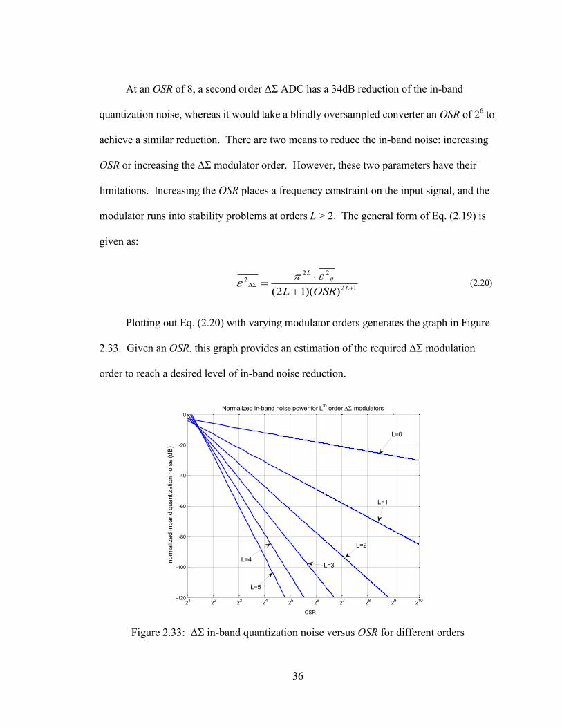
At an OSR of 8, a second order ΔΣ ADC has a 34dB reduction of the in-band
quantization noise, whereas it would take a blindly oversampled converter an OSR of 26 to
achieve a similar reduction. There are two means to reduce the in-band noise: increasing
OSR or increasing the ΔΣ modulator order. However, these two parameters have their
limitations. Increasing the OSR places a frequency constraint on the input signal, and the
modulator runs into stability problems at orders L > 2. The general form of Eq. (2.19) is
given as:
12
222
))(12(
L
qL
OSRL
(2.20)
Plotting out Eq. (2.20) with varying modulator orders generates the graph in Figure
2.33. Given an OSR, this graph provides an estimation of the required ΔΣ modulation
order to reach a desired level of in-band noise reduction.
Figure 2.33: ΔΣ in-band quantization noise versus OSR for different orders
-120
-100
-80
-60
-40
-20
0
Normalized in-band noise power for Lth
order modulators
21 22 23 24 25 26 27 28 29 210
no
rma
lize
d in
ba
nd
qu
an
tiza
tio
n n
ois
e (
dB
)
OSR
L=4
L=5
L=3
L=2
L=1
L=0

37
2.3.3. ΔΣ Modulator Loop Filter
The high-pass response of the ΔΣ modulator affects only the quantization noise.
The signal ideally passes through unperturbed. Figure 2.34 is the Z-domain linear model
for a second order ΔΣ modulator. The input signal U is passed through two filters, H1(z)
and H2(z), before being quantized. The quantizer is represented as an additive
quantization noise signal, Q. The quantized output, V, is then subtracted from the input
path. The modulator continuously sums up the difference between the filtered input and
the quantized output (the Σ of the Δ’s).
+U H1(z) +C
H2(z)B A
V
-+
Q
z-1
-
Figure 2.34: Standard linearized model for second order ΔΣ modulation
The transfer function of the modulator is calculated by introducing a few
intermediate nodes, A, B, and C, and defining them as:
QAV , BHA 2 , VzCB 1 , )( 1
1 VzUHC (2.21)
Eliminating all the intermediate terms yields the output in terms of only the input
and quantization noise:
VHHzUHHVHzQV 21
1
212
1 (2.22)
38
U
HHzHz
HHQ
HHzHzV
21
1
2
1
21
21
1
2
1 11
1
(2.23)
The result in Eq. (2.23) indicates that the output is composed of the input and
quantization noise, each with its own transfer function. The desired transfer function for
the quantization noise is a second order high-pass response while leaving the input alone.
Defining the noise transfer function (NTF) and signal transfer function (STF) with their
respective Z-domain responses yields:
21
21
1
2
1)1(
1
1
z
HHzHzNTF
11 21
1
2
1
21
HHzHz
HHSTF
(2.24)
Solving Eq. (2.24) provides a standardized and easily realizable form for each of the
cascaded filters:
1211
1
z
HH (2.25)
2.3.4. ΔΣ Simulink Model
The architecture used for the model is from [20], shown in Figure 2.35. This has a
feedback and feed-forward in the modulator structure. U and M have the same number of
bits. Following empiric simulated results done in [20], U was chosen to from between ±M
/2 for well-behaved results. When U is chosen outside of these limits, it increases the
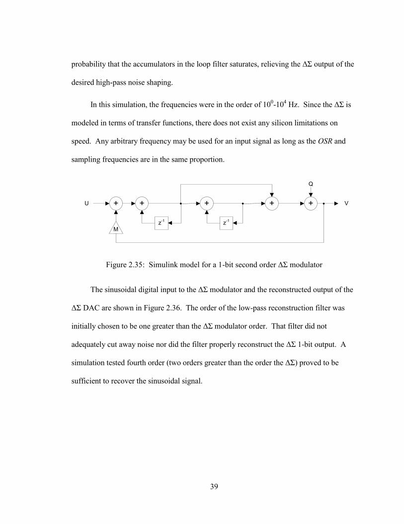
39
probability that the accumulators in the loop filter saturates, relieving the ΔΣ output of the
desired high-pass noise shaping.
In this simulation, the frequencies were in the order of 100-10
4 Hz. Since the ΔΣ is
modeled in terms of transfer functions, there does not exist any silicon limitations on
speed. Any arbitrary frequency may be used for an input signal as long as the OSR and
sampling frequencies are in the same proportion.
+
z-1
+ +
Q
+
z-1
VU +
M
Figure 2.35: Simulink model for a 1-bit second order ΔΣ modulator
The sinusoidal digital input to the ΔΣ modulator and the reconstructed output of the
ΔΣ DAC are shown in Figure 2.36. The order of the low-pass reconstruction filter was
initially chosen to be one greater than the ΔΣ modulator order. That filter did not
adequately cut away noise nor did the filter properly reconstruct the ΔΣ 1-bit output. A
simulation tested fourth order (two orders greater than the order the ΔΣ) proved to be
sufficient to recover the sinusoidal signal.

40
Figure 2.36: 1-bit quantized second order ΔΣ modulator transient results
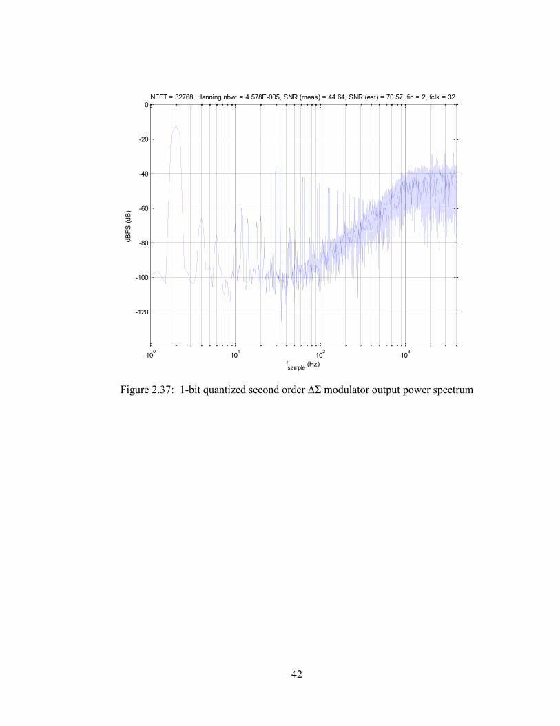
The input signal frequency was chosen to fall within an exact FFT bin as to avoid
spectral smearing [19]. Due to the lack of a digital interpolation filter on the input to the
ΔΣ modulator, the power spectrum, Figure 2.37, shows significant frequency components
within the pass-band. These frequency spikes occur on multiples of the input sinusoid
frequency. Likewise, the analog to digital quantization of an idealized sinusoidal
introduced many frequency components due to the sampling with respect to the converter
clock. The first three spikes presented on the spectrum plot are the signal (first spike) and
the harmonics of this low frequency input.
0 0.5 1 1.5 2 2.5 3 3.5 4 4.5 50
50
100
150
200
250
dig
ital code
8-bit quantized sinusoidal input to modulator
0 0.5 1 1.5 2 2.5 3 3.5 4 4.5 5
0
0.2
0.4
0.6
0.8
1
VO
UT (
V)
time (s)
Analog filter reconstructed output

41
The function of an interpolation filter is to increase the sampling rate by zero-
padding the oversampled results [19]. For example, passing an input with frequency fin
through an 8x interpolation filter will produce an output at 16x fin. The interpolation filter
output has the first sample of the input followed by 7 zeros, a second sample of the input
followed by 7 zeros, and so on. The input signal is thus given an artificial high-frequency
sampling component, pushing these sampling-related harmonics beyond the pass-band.
Using an approximate calculation, assuming an interpolation filter was sufficient to
remove the input harmonics within the pass-band, an estimated “SNR (est)” was
calculated. The Matlab code for this estimation simply ignores the harmonics within the
pass-band when calculating SNR.
The pairs of harmonic spikes that occur further past the signal bandwidth are caused
by the sampling clock mixing with the signal frequency. The input signal is 2 Hz and the
digital quantization was clocked at 32 Hz. At every multiple of 32 Hz, a pair of spikes 2
Hz apart is the result of these frequencies mixing. Finally, the power spectrum of the
higher frequencies of the ΔΣ modulator exhibits the theorized +40 dB/dec second order
high-pass response.
42
Figure 2.37: 1-bit quantized second order ΔΣ modulator output power spectrum
100
101
102
103
-120
-100
-80
-60
-40
-20
0
fsample
(Hz)
dB
FS
(dB
)
NFFT = 32768, Hanning nbw: = 4.578E-005, SNR (meas) = 44.64, SNR (est) = 70.57, fin = 2, fclk = 32

43
Chapter 3. Techniques for CDR Jitter Reduction
The last chapter introduced the building blocks for CDRs and discussed some
limitations in their design. Many techniques are currently available for alleviating these
jitter limitations in CDRs. This chapter covers an analog modification to the phase mixer
in a standard PI and two novel CDR architectures.
3.1. Nested Phase Interpolation
The nested phase interpolator [21] CDR follows the same architecture as a standard
PI except it utilizes a nested interpolator. While the standard PI breaks up its control word
into a mux selection and α, the nested PI further separates α into a αcourse and αfine. The
goal is to use cascaded stages of lower resolution interpolation orders, shown in Figure
3.1, to save on area and power.
The mux selection provides the initial two adjacent clock phases, ΦM and ΦM+1, to
the coarse interpolators. These interpolators are driven by αcoarse and αcoarse+1 in order to
generate two adjacent coarsely interpolated phases. Finally, the αfine drives the fine phase
interpolator to arrive at the final ΦOUT. A nested design of equal resolution to a standard
PI can offer much lower power and area consumption.

44
Coarse
Phase
Interpolator
C-bitsCoarse
α
Coarse
Phase
Interpolator
Fine
Phase
Interpolator
Φcα
Φcα+1
ΦOUT
C-bitsCoarse
α+1
ΦM,ΦM+1
2
F-bitsFine
α
Figure 3.1: Nested PI block diagram
Discussed previously, a typical phase mixer with an M-bit α control word will have
2M current legs. A nested interpolator design has two C-bit coarse interpolators driving
an F-bit fine interpolator for the final output clock, where F = M - C.
The number of current legs in a traditional phase mixer (left side of inequality) can
be related to the nested design by:
CMC
M 222
2
2 (3.1)
Rearranging the inequality and splitting up the left hand side into two parts then
taking the log2 of both sides yield:
CMCMM 2222 122 (3.2)
12 CM , CMM 2 (3.3)
45
Solving for M and C results in the lower limits of M ≥ 5 and C ≥ 3. When a nested
PI is designed with these bounding conditions, the total number of current legs used by
will be less than half of a standard PI.
3.2. Averaging Phase Interpolation
Covered in the previous chapter, a standard PI CDR has systematic jitter limited by
the resolution of the control word. As there is a practical and power limitation on
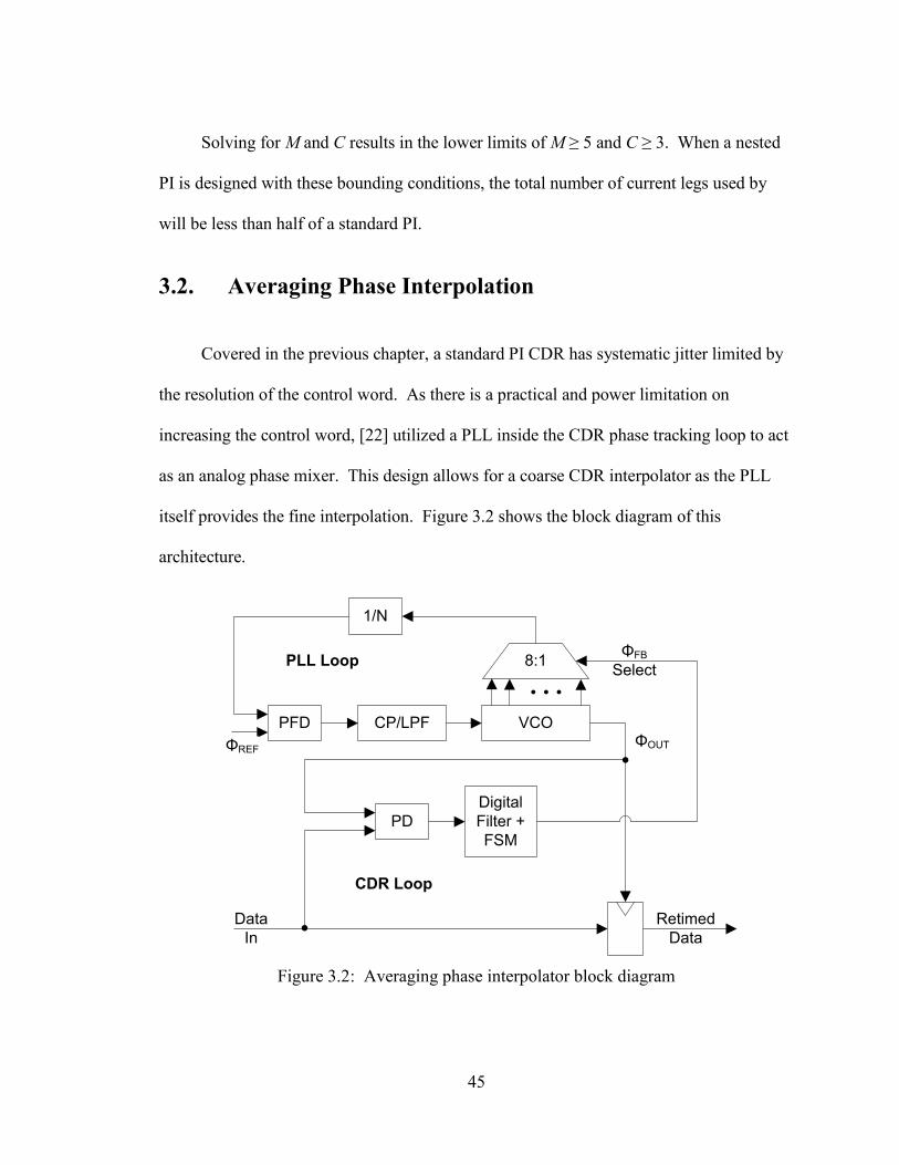
increasing the control word, [22] utilized a PLL inside the CDR phase tracking loop to act
as an analog phase mixer. This design allows for a coarse CDR interpolator as the PLL
itself provides the fine interpolation. Figure 3.2 shows the block diagram of this
architecture.
PFD CP/LPF VCO
1/N
ΦOUTΦREF
Retimed
Data
PD
Data
In
Digital
Filter +
FSM
ΦFB
SelectPLL Loop
CDR Loop
8:1
Figure 3.2: Averaging phase interpolator block diagram

46
The interpolation in this design comes from the PLL loop filter. The PLL initially
locks onto the reference frequency and generates K evenly spaced clocks from a multi-
phase VCO. Using a single ΦOUT from the VCO, the CDR loop generates a control word
that selects one of the VCO phases as the PLL feedback. As the feedback clock changes,
the PLL loop forces the VCO to slowly shift towards the new clock phase. As the
feedback phase selection is changing between ΦM and ΦM+1, the PLL loop filter causes the
control voltage to settle on a phase in between the two selections.
The averaging phase interpolation uses a digital FSM-based implementation for the
coarse interpolator to eliminate the analog requirements of a traditional PI. The chosen
phases ΦM and ΦM+1 are selected by the FSM with an interpolation weighting α, producing
a repeated pattern of ΦM and ΦM+1 to use as the PLL feedback. In [22], the pattern was
given over four clock cycles, allowing this implementation a coarse interpolation in steps
of 25% between ΦM and ΦM+1. With this design, the clocking jitter was limited by the
VCO noise.
3.2.1. Simulink Modeled Results
The model for this architecture, shown in Figure 3.3, uses an 8-bit control word
from the CDR loop to control the FSM-based phase averaging. The control word has the
3 MSB represent the mux selection, the next 3 bits represent the coarse interpolator α, and
the final 2 LSB are the FSM phase averaging pattern control.
The same PLL from Chapter 2 was modified with an 8-phase VCO, but the loop
parameters are the same as before. The coarse phase interpolator inside the 8-phase VCO
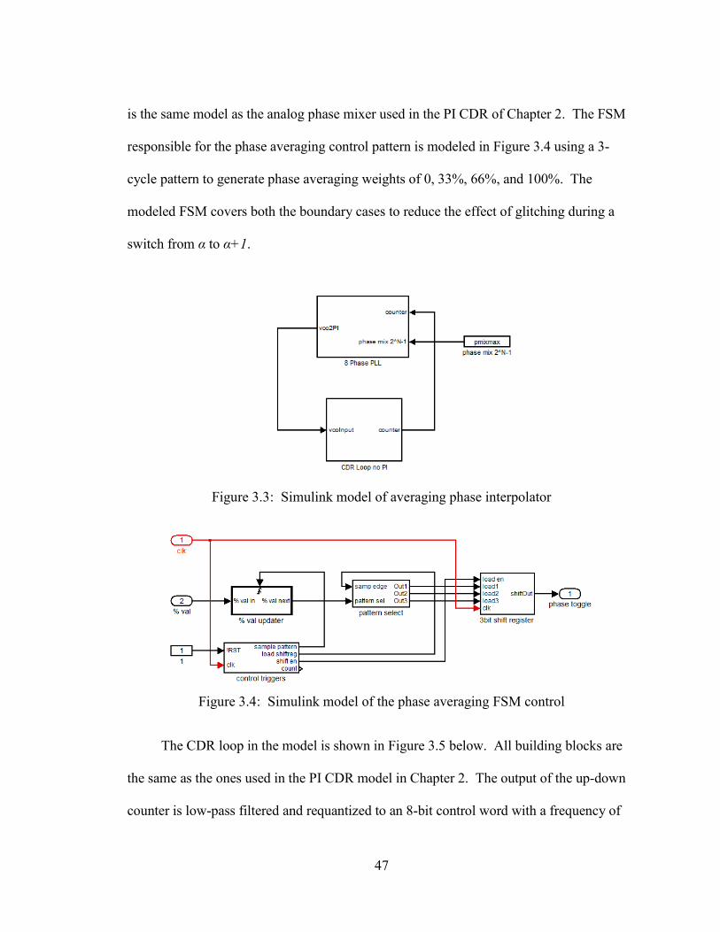
47
is the same model as the analog phase mixer used in the PI CDR of Chapter 2. The FSM
responsible for the phase averaging control pattern is modeled in Figure 3.4 using a 3-
cycle pattern to generate phase averaging weights of 0, 33%, 66%, and 100%. The
modeled FSM covers both the boundary cases to reduce the effect of glitching during a
switch from α to α+1.
Figure 3.3: Simulink model of averaging phase interpolator
Figure 3.4: Simulink model of the phase averaging FSM control
The CDR loop in the model is shown in Figure 3.5 below. All building blocks are
the same as the ones used in the PI CDR model in Chapter 2. The output of the up-down
counter is low-pass filtered and requantized to an 8-bit control word with a frequency of
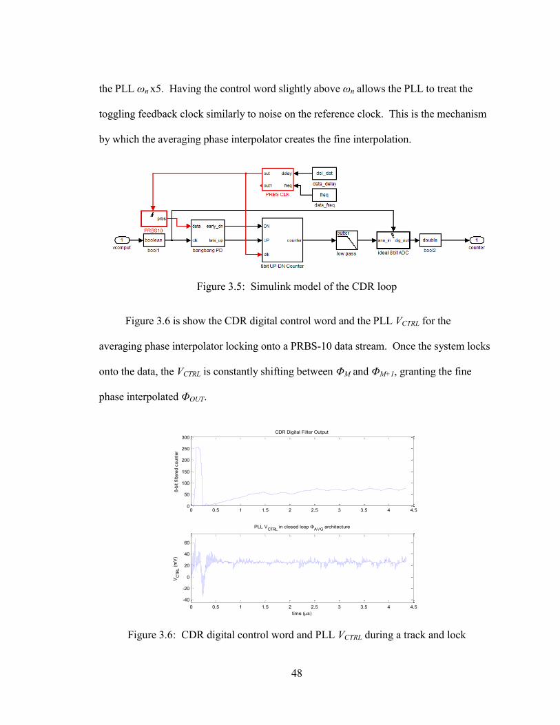
48
the PLL ωn x5. Having the control word slightly above ωn allows the PLL to treat the
toggling feedback clock similarly to noise on the reference clock. This is the mechanism
by which the averaging phase interpolator creates the fine interpolation.
Figure 3.5: Simulink model of the CDR loop
Figure 3.6 is show the CDR digital control word and the PLL VCTRL for the
averaging phase interpolator locking onto a PRBS-10 data stream. Once the system locks
onto the data, the VCTRL is constantly shifting between ΦM and ΦM+1, granting the fine
phase interpolated ΦOUT.
Figure 3.6: CDR digital control word and PLL VCTRL during a track and lock
0 0.5 1 1.5 2 2.5 3 3.5 4 4.50
50
100
150
200
250
300
8-b
it f
iltere
d c
ounte
r
CDR Digital Filter Output
0 0.5 1 1.5 2 2.5 3 3.5 4 4.5
-40
-20
0
20
40
60
VC
TR
L (
mV
)
time (s)
PLL VCTRL
in closed loop AVG
architecture
49
There are a couple drawbacks to this design. Since the CDR is essentially PLL-
driven, the response time of the data tracking is bound by ωn. This can be adjusted by
changing the ωn of the PLL, but that involves increasing the reference frequency in order
to maintain PLL loop stability. The second and more critical drawback is the frequency
component caused by the repeated patterns from the FSM. For a coarse interpolation of
33%, the FSM outputs ΦM for two clock cycles followed by one cycle of ΦM+1. This
pattern makes an impact on the frequency response of the system. Employing a ΔΣ
modulator to randomize the FSM pattern can alleviate this limitation.
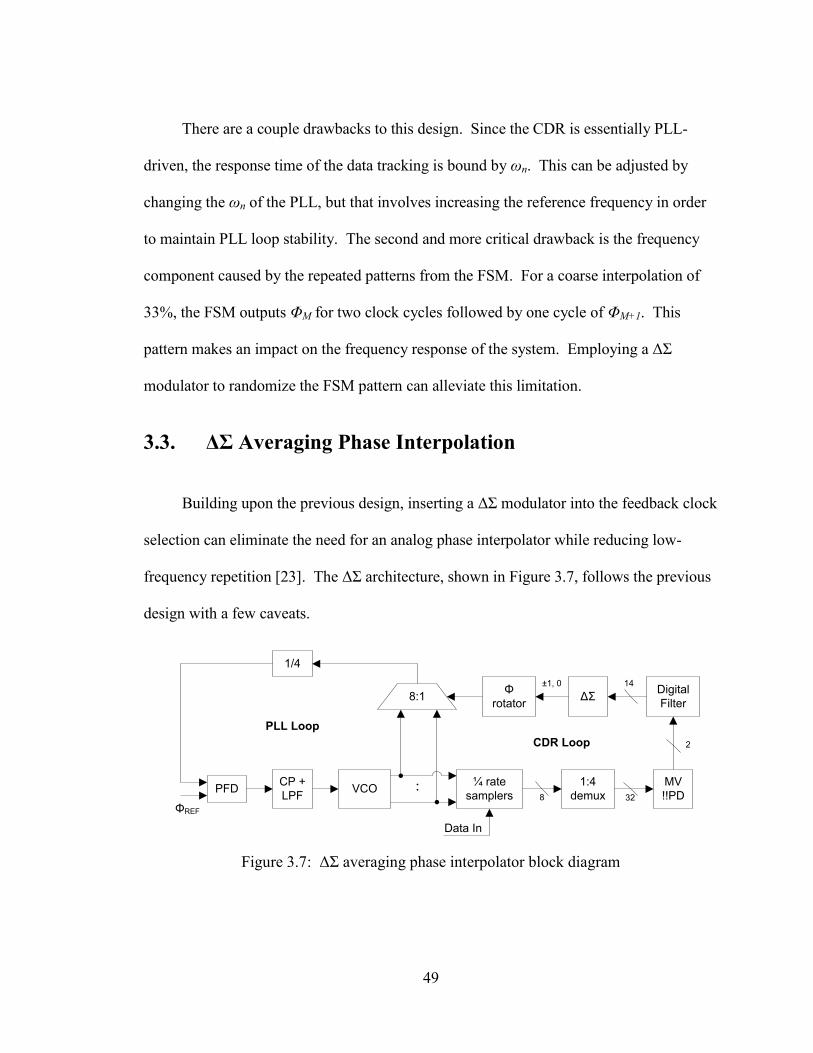
3.3. ΔΣ Averaging Phase Interpolation
Building upon the previous design, inserting a ΔΣ modulator into the feedback clock
selection can eliminate the need for an analog phase interpolator while reducing low-
frequency repetition [23]. The ΔΣ architecture, shown in Figure 3.7, follows the previous
design with a few caveats.
PFDCP +
LPFVCO
1/4
ΦREF
Data In
PLL Loop
8:1
¼ rate
samplers
1:4
demux
MV
!!PD
Digital
FilterΔΣ
Φ
rotator
CDR Loop
8 32
2
14±1, 0
Figure 3.7: ΔΣ averaging phase interpolator block diagram
50
This ΔΣ architecture uses a quarter-rate !!PD in the CDR loop to demultiplex the
incoming data stream. After going through two more stages of half-rate demultiplexing,
the decision-making logic only requires a clock of fDAT /16. The demuxed phase detector
outputs are then majority voted to produce a single !!PD decision which is given to a
proportional and integral dual-path digital filter. This filter output is the control word for
the PLL feedback selection. Passing the control word through a tri-level quantized second
order error-feedback ΔΣ modulator with 8x OSR produces a stream of -1, 0, and +1. This
controls a phase rotator implemented as a circular shift register which selects the PLL
feedback phase. By means of the ΔΣ modulator, the interpolation control is no longer a
repetitious FSM sequence.
3.3.1. Second Order Error-Feedback ΔΣ Modulator
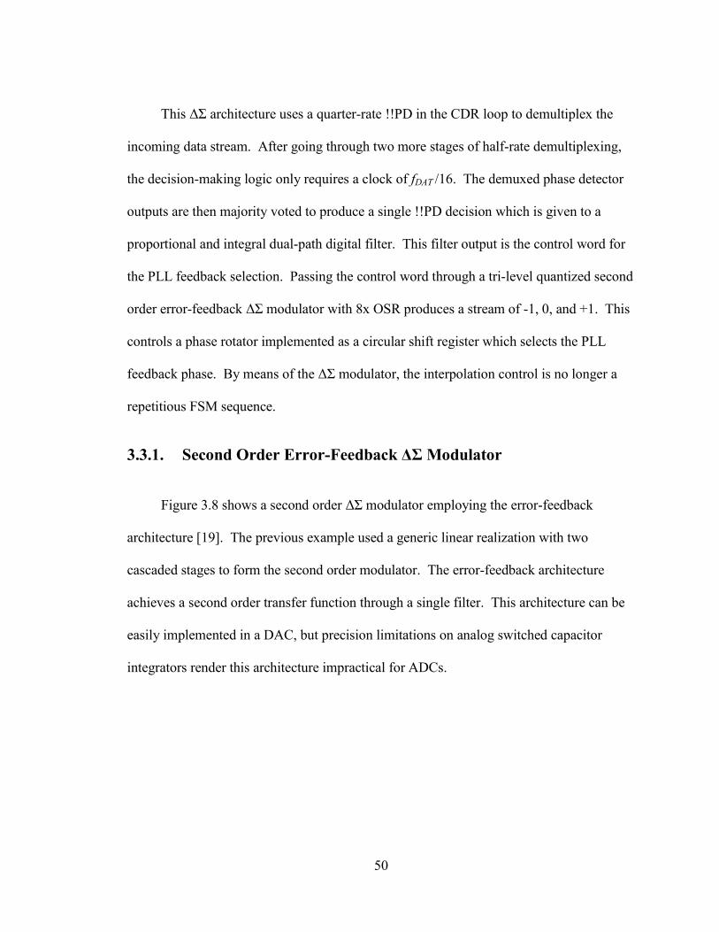
Figure 3.8 shows a second order ΔΣ modulator employing the error-feedback
architecture [19]. The previous example used a generic linear realization with two
cascaded stages to form the second order modulator. The error-feedback architecture
achieves a second order transfer function through a single filter. This architecture can be
easily implemented in a DAC, but precision limitations on analog switched capacitor
integrators render this architecture impractical for ADCs.
51
HE(z) = 2z-1
-z-2
+
+z-1
-e
Y
-
VU
z-1
+
- 2
+
Q
Figure 3.8: Second order error feedback architecture
The error-feedback architecture utilizes the error from quantization, e, instead of the
quantized output itself. The error is passed through a second order filter and added back
into the input signal. Similar to the previous analysis of the generic cascaded modulator,
the output V is expressed in terms of the signal and error:
eYVVYe , eHUY E (3.4)
eHUeeHUV EE )1( (3.5)
Then Eq. (3.5) is equated with the desired NTF and STF and the filter transfer
function is derived as:
21)1(1 zHNTF E , 1STF (3.6)
212 zzHE (3.7)
52
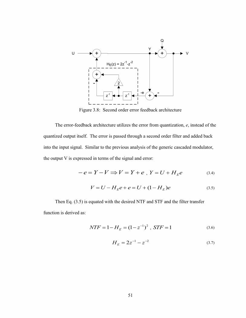
3.3.2. Simulink Modeled Error-Feedback ΔΣ Results
The error-feedback ΔΣ modulator used in [23] had a 3-level output, allowing the ΔΣ
modulator output to select between ΦS-1, ΦS, and ΦS+1 to give a range of ±50% from ΦS.
In this model the same ΔΣ modulator output was sent to a low-pass filter to show the DC
average of the output. The results in Figure 3.9 were in agreement with Eq. (3.6), when
the DC input is the minimum allowed for well-behaved results, the DC output settled to -
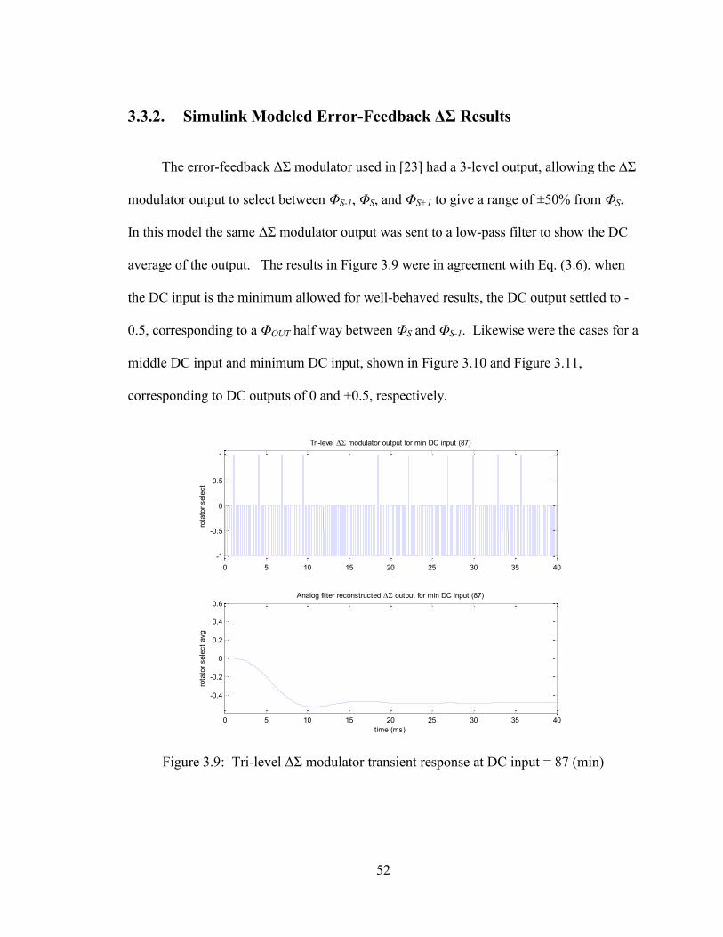
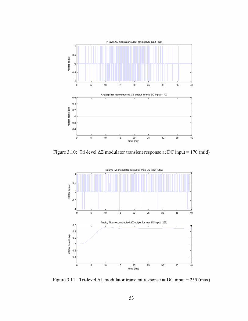
0.5, corresponding to a ΦOUT half way between ΦS and ΦS-1. Likewise were the cases for a
middle DC input and minimum DC input, shown in Figure 3.10 and Figure 3.11,
corresponding to DC outputs of 0 and +0.5, respectively.
Figure 3.9: Tri-level ΔΣ modulator transient response at DC input = 87 (min)
0 5 10 15 20 25 30 35 40
-1
-0.5
0
0.5
1
rota
tor
sele
ct
Tri-level modulator output for min DC input (87)
0 5 10 15 20 25 30 35 40
-0.4
-0.2
0
0.2
0.4
0.6
rota
tor
sele
ct
avg
time (ms)
Analog filter reconstructed output for min DC input (87)
53
Figure 3.10: Tri-level ΔΣ modulator transient response at DC input = 170 (mid)
Figure 3.11: Tri-level ΔΣ modulator transient response at DC input = 255 (max)
0 5 10 15 20 25 30 35 40
-1
-0.5
0
0.5
1
rota
tor
sele
ct
Tri-level modulator output for mid DC input (170)
0 5 10 15 20 25 30 35 40
-0.4
-0.2
0
0.2
0.4
0.6
rota
tor
sele
ct
avg
time (ms)
Analog filter reconstructed output for mid DC input (170)
0 5 10 15 20 25 30 35 40
-1
-0.5
0
0.5
1
rota
tor
sele
ct
Tri-level modulator output for max DC input (255)
0 5 10 15 20 25 30 35 40
-0.4
-0.2
0
0.2
0.4
0.6
rota
tor
sele
ct
avg
time (ms)
Analog filter reconstructed output for max DC input (255)
54
3.3.3. Simulink Modeled Top-level Results
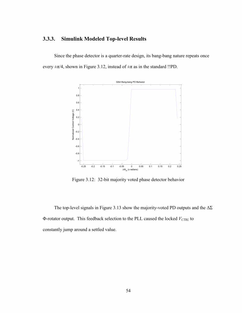
Since the phase detector is a quarter-rate design, its bang-bang nature repeats once
every ±π/4, shown in Figure 3.12, instead of ±π as in the standard !!PD.
Figure 3.12: 32-bit majority voted phase detector behavior
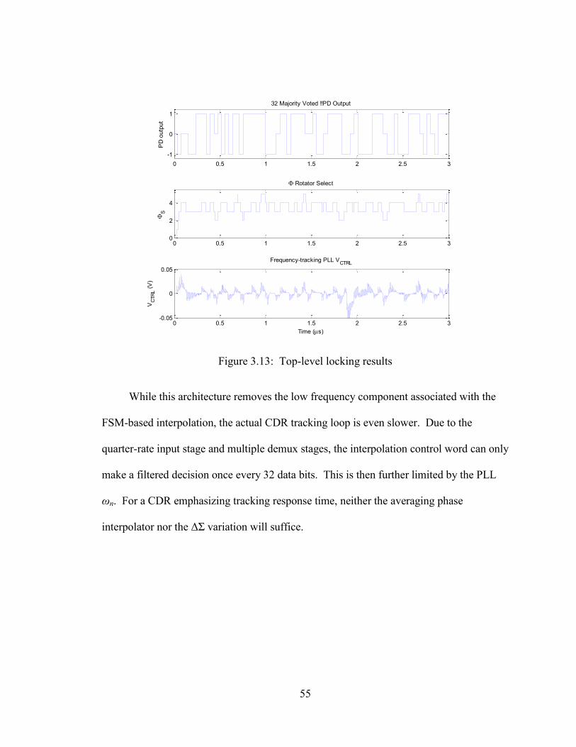
The top-level signals in Figure 3.13 show the majority-voted PD outputs and the ΔΣ
Φ-rotator output. This feedback selection to the PLL caused the locked VCTRL to
constantly jump around a settled value.
-0.25 -0.2 -0.15 -0.1 -0.05 0 0.05 0.1 0.15 0.2 0.25
-1
-0.8
-0.6
-0.4
-0.2
0
0.2
0.4
0.6
0.8
1
32bit Bang-bang PD Behavior
in
( radians)
Norm
aliz
ed C
ontr
ol V
oltage (
V)
55
Figure 3.13: Top-level locking results
While this architecture removes the low frequency component associated with the
FSM-based interpolation, the actual CDR tracking loop is even slower. Due to the
quarter-rate input stage and multiple demux stages, the interpolation control word can only
make a filtered decision once every 32 data bits. This is then further limited by the PLL
ωn. For a CDR emphasizing tracking response time, neither the averaging phase
interpolator nor the ΔΣ variation will suffice.
0 0.5 1 1.5 2 2.5 3
-1
0
1
PD
outp
ut
32 Majority Voted !!PD Output
0 0.5 1 1.5 2 2.5 30
2
4
S
Rotator Select
0 0.5 1 1.5 2 2.5 3-0.05
0
0.05
VC
TR
L (
V)
Time (s)
Frequency-tracking PLL VCTRL
56
Chapter 4. Lock Detection
None of the previously discussed techniques address the limitation of the Alexander
phase detector. No matter how well the feedback clock is held constant, so long as the
!!PD does not stop detection during a locked state, the PI control logic will always have
jitter. The only method to solve this underlying issue is to detect when the CDR is in lock
and disable the phase detector. Before the design of a lock detector can be implemented,
the strengths and weaknesses of similar techniques are first explored.
4.1. Techniques Related to CDR Lock Detection
The concept of lock detection has already been used in many existing systems [24],
[25]. Two key components for a lock detection scheme are the lock detector itself and an
in-lock mode. The lock detection is merely a monitor within the decision-making loop
that can detect when the system can be considered “in lock.” Vital components within the
control loop can then use this in-lock flag to toggle between tracking mode and an in-lock
mode.
For PLL/DLLs and CDRs, the phase detector is the most critical component in the
control loop, and lock detection can be implemented by monitoring the control voltage
from the detector output. Some techniques that accomplish this are control voltage
thresholds and tri-state phase detectors.

57
4.1.1. Control Voltage Thresholds
In [24], lock detection was achieved in a PI CDR using a linear phase detector and
an analog filter to locate an in-lock control voltage. Similarly, analog VCO control
voltage with thresholds can be used to determine lock in type-II PLLs. However, a digital
control is preferred for maintaining scalability and accuracy.
Digital lock detection was employed for a clock multiplying PLL with a delay-
locked loop (DLL) in [25]. It generates two pulses of length T (an in-lock threshold) for
the reference and feedback clocks to increment a duration counter. Once this duration
counter reaches its limit, the system recognizes a frequency lock and is switched into DLL
mode until it leaves lock. However, this technique does not address jitter from the DLL
mode itself.
4.1.2. Tri-state Phase Detectors
Tri-state !!PDs were developed in charge-pump PLL type CDRs to reduce the
charge pump’s effect on the control voltage [26], [27]. During a no-change PD output, the
charge-pump is allowed to neither charge nor discharge the capacitor. This forces the
control voltage of the oscillator to remain constant. Since these are binary phase detectors,
they follow Alexander’s equations and are limited to outputting a no-change only during a
period of non-transitioning data.
58
A dual-path charge-pump PLL type CDR employs a “three-state” phase and
frequency detector in [28]. The phase detector is a half-rate multiplexed design. Once in
lock, two of the phase detectors sample the data and two sample the transitions. Control
logic halts the frequency tracking during the locked state, effectively holding the oscillator
control voltage constant. This design utilizes the loop filter to smooth out the bang-bang
nature of the phase detector while control logic disables the frequency loop.
These binary detectors all have a mechanism to reduce the effect of the bang-bang
effect, but they are still limited by Alexander’s equations. In order to eliminate the
systematic PI jitter, a !!PD needs to be able to distinguish between a no-change and in-
lock state.
4.2. Proposed Lock Detection
The proposed lock detection combined the concepts of a tri-state phase detector with
a digital control word threshold. Since the heart of the PI control is a counter, two digital
thresholds need to be set as boundaries. Once the counter remains within these thresholds
for a number of clock cycles, the system recognizes lock and stop the !!PD from affecting
the feedback. The design behind the proposed lock detection technique and the modeled
results are detailed in the following sections.
4.2.1. Lock Detection PI Design
The logic flowchart of the lock detection PI is shown in Figure 4.1. Two
configurable parameters define the “in-lock” status: a configurable threshold, T, and

59
locking cycle count, L. In order to flag a lock, the live counter must remain within X ± T
for L clock cycles. Each time the counter passes the threshold, X updates to the new
counter value. Once the CDR is locked, the analog phase mixer receives the constant X
control word instead of the live counter toggling between a few in-lock values.
Stored count = X
Threshold = T
Lock counter limit = L
Counter > X+T
OR
Counter < X-T
Locking counter +1
Locking counter
>= L
NO
Update Counter
NO
X = Counter
LOCK = 0
Locking counter = 0
YES
LOCK = 1
Locking counter fixed
Alpha/MUXSEL fixedYES
InitializationCounter = 0
X = 0
LOCK = 0
Locking counter = 0
Figure 4.1: Lock detect PI logic flowchart
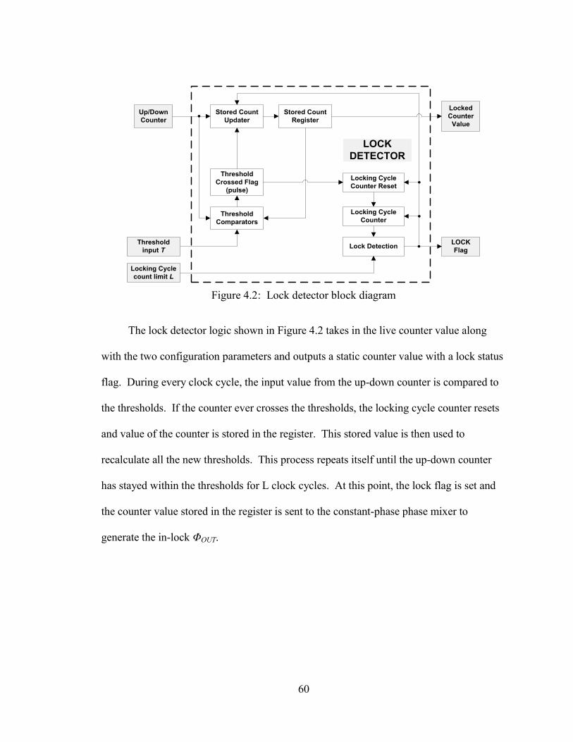
60
Stored Count
Updater
Up/Down
Counter
Threshold
Comparators
Stored Count
Register
Threshold
input T
Threshold
Crossed Flag
(pulse)
Locking Cycle
Counter Reset
Locking Cycle
Counter
Locking Cycle
count limit L
Lock DetectionLOCK
Flag
LOCK
DETECTOR
Locked
Counter
Value
Figure 4.2: Lock detector block diagram
The lock detector logic shown in Figure 4.2 takes in the live counter value along
with the two configuration parameters and outputs a static counter value with a lock status
flag. During every clock cycle, the input value from the up-down counter is compared to
the thresholds. If the counter ever crosses the thresholds, the locking cycle counter resets
and value of the counter is stored in the register. This stored value is then used to
recalculate all the new thresholds. This process repeats itself until the up-down counter
has stayed within the thresholds for L clock cycles. At this point, the lock flag is set and
the counter value stored in the register is sent to the constant-phase phase mixer to
generate the in-lock ΦOUT.
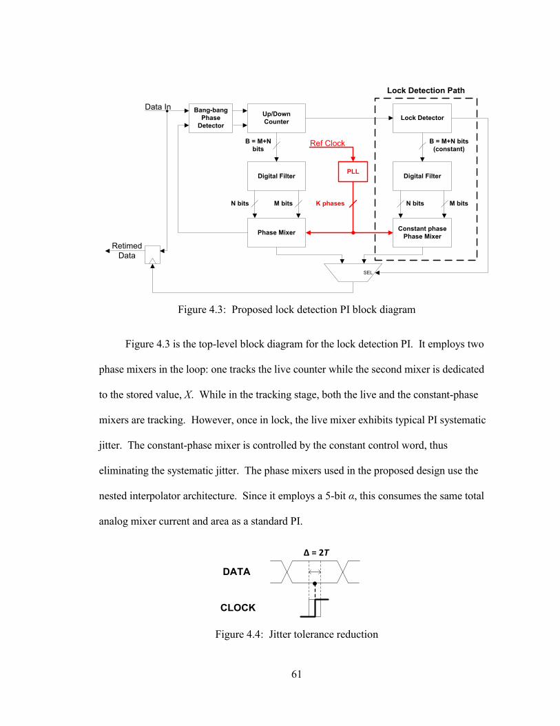
61
B = M+N bits
(constant)
N bits
Bang-bang
Phase
Detector
Up/Down
Counter
Digital Filter
Phase Mixer
PLL
Lock Detector
Digital Filter
Constant phase
Phase Mixer
M bits
B = M+N
bits
N bits M bitsK phases
Data In
Retimed
Data
SEL
Ref Clock
Lock Detection Path
Figure 4.3: Proposed lock detection PI block diagram
Figure 4.3 is the top-level block diagram for the lock detection PI. It employs two
phase mixers in the loop: one tracks the live counter while the second mixer is dedicated
to the stored value, X. While in the tracking stage, both the live and the constant-phase
mixers are tracking. However, once in lock, the live mixer exhibits typical PI systematic
jitter. The constant-phase mixer is controlled by the constant control word, thus
eliminating the systematic jitter. The phase mixers used in the proposed design use the
nested interpolator architecture. Since it employs a 5-bit α, this consumes the same total
analog mixer current and area as a standard PI.
Δ = 2T
DATA
CLOCK
Figure 4.4: Jitter tolerance reduction
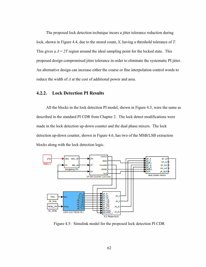
62
The proposed lock detection technique incurs a jitter tolerance reduction during
lock, shown in Figure 4.4, due to the stored count, X, having a threshold tolerance of T.
This gives a Δ = 2T region around the ideal sampling point for the locked state. This
proposed design compromised jitter tolerance in order to eliminate the systematic PI jitter.
An alternative design can increase either the coarse or fine interpolation control words to
reduce the width of Δ at the cost of additional power and area.
4.2.2. Lock Detection PI Results
All the blocks in the lock detection PI model, shown in Figure 4.5, were the same as
described in the standard PI CDR from Chapter 2. The lock detect modifications were
made in the lock detection up-down counter and the dual phase mixers. The lock
detection up-down counter, shown in Figure 4.6, has two of the MSB/LSB extraction
blocks along with the lock detection logic.
Figure 4.5: Simulink model for the proposed lock detection PI CDR
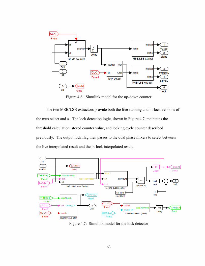
63
Figure 4.6: Simulink model for the up-down counter
The two MSB/LSB extractors provide both the free-running and in-lock versions of
the mux select and α. The lock detection logic, shown in Figure 4.7, maintains the
threshold calculation, stored counter value, and locking cycle counter described
previously. The output lock flag then passes to the dual phase mixers to select between
the live interpolated result and the in-lock interpolated result.
Figure 4.7: Simulink model for the lock detector
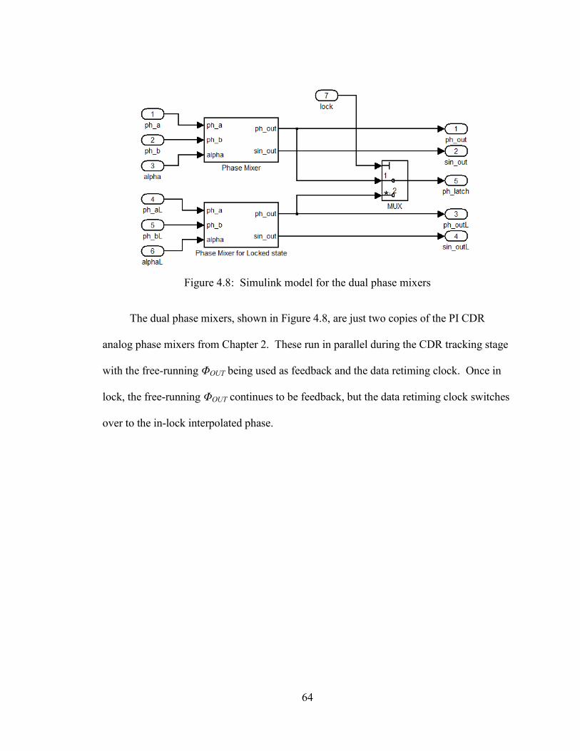
64
Figure 4.8: Simulink model for the dual phase mixers
The dual phase mixers, shown in Figure 4.8, are just two copies of the PI CDR
analog phase mixers from Chapter 2. These run in parallel during the CDR tracking stage
with the free-running ΦOUT being used as feedback and the data retiming clock. Once in
lock, the free-running ΦOUT continues to be feedback, but the data retiming clock switches
over to the in-lock interpolated phase.
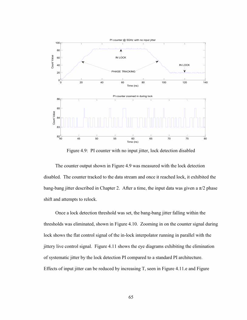
65
Figure 4.9: PI counter with no input jitter, lock detection disabled
The counter output shown in Figure 4.9 was measured with the lock detection
disabled. The counter tracked to the data stream and once it reached lock, it exhibited the
bang-bang jitter described in Chapter 2. After a time, the input data was given a π/2 phase
shift and attempts to relock.
Once a lock detection threshold was set, the bang-bang jitter falling within the
thresholds was eliminated, shown in Figure 4.10. Zooming in on the counter signal during
lock shows the flat control signal of the in-lock interpolator running in parallel with the
jittery live control signal. Figure 4.11 shows the eye diagrams exhibiting the elimination
of systematic jitter by the lock detection PI compared to a standard PI architecture.
Effects of input jitter can be reduced by increasing T, seen in Figure 4.11.e and Figure
0 20 40 60 80 100 120 1400
20
40
60
80
100PI counter @ 5GHz with no input jitter
Count
Valu
e
Time (ns)
40 45 50 55 60 65 70 75 8082
83
84
85
86PI counter zoomed in during lock
Count
Valu
e
Time (ns)
IN LOCK
IN LOCK
PHASE TRACKING
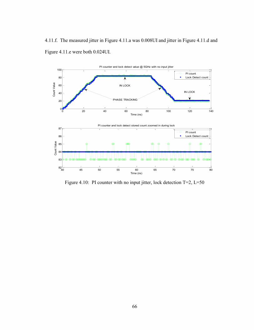
66
4.11.f. The measured jitter in Figure 4.11.a was 0.008UI and jitter in Figure 4.11.d and
Figure 4.11.e were both 0.024UI.
Figure 4.10: PI counter with no input jitter, lock detection T=2, L=50
0 20 40 60 80 100 120 1400
20
40
60
80
100PI counter and lock detect value @ 5GHz with no input jitter
Time (ns)
Count
Valu
e
PI count
Lock Detect count
40 45 50 55 60 65 70 75 8082
83
84
85
86
87PI counter and lock detect stored count zoomed in during lock
Time (ns)
Count
Valu
e
PI count
Lock Detect count
IN LOCK
IN LOCK
PHASE TRACKING

67
Figure 4.11: Eye diagrams for various lock detect setups
050
100
150
200
-0.20
0.2
0.4
0.6
0.81
1.2
no input
jitt
er,
lock d
ete
ct
dis
able
d
(a)
Voltage (V)
050
100
150
200
-0.20
0.2
0.4
0.6
0.81
1.2
no input
jitt
er,
lock d
ete
ct
T =
2
(b)
050
100
150
200
-0.20
0.2
0.4
0.6
0.81
1.2
no input
jitt
er,
lock d
ete
ct
T =
4
(c)
050
100
150
200
-0.20
0.2
0.4
0.6
0.81
1.2
0.0
1U
I in
put
jitt
er,
lock d
ete
ct
dis
able
d
Tim
e (
ps)
Voltage (V)
050
100
150
200
-0.20
0.2
0.4
0.6
0.81
1.2
0.0
1U
I in
put
jitt
er,
lock d
ete
ct
T =
2
Tim
e (
ps)
050
100
150
200
-0.20
0.2
0.4
0.6
0.81
1.2
0.0
1U
I in
put
jitt
er,
lock d
ete
ct
T =
4
Tim
e (
ps)
(d)
(e)
(f)
68
Chapter 5. Conclusions
With the ever-increasing need for higher data rates on inter-chip communications,
CDR technology has to be refined in order to maintain quality. As clock speeds increase
and voltage levels decrease, more importance is placed on fast and accurate recovery.
Dual-loop PLL-PI clock and data recovery systems are attractive for use in source-
synchronous clock receivers with multiple data lanes. However, their architectural jitter
limitations pose a challenge for designers.
The building blocks for dual-loop PLL-PI architectures were explored for possible
modifications in order to reduce systematic jitter. ΔΣ modulation was also examined as a
potential means to shape the systematic jitter to higher frequencies. Three existing
technologies that aim to reduce phase interpolation jitter were studied in order to
understand the limitations in various architectures.
Many existing methods of lock detection and control voltage thresholding were
compared and improved upon to reach the proposed design of a lock detection phase
interpolator CDR. The proposed design successfully eliminated phase interpolator
systematic jitter at the cost of reduced jitter tolerance. The successful modeling of the
lock detection PI CDR opens the way to further testing of this concept and efforts can be
turned towards transistor-level design.
69
References
[1] "Cisco Visual Networking Index: Global Mobile Data Traffic Forecast Update,
2012-2017," Feb. 2013. [Online]. Available:
http://www.cisco.com/en/US/solutions/collateral/ns341/ns525/ns537/ns705/ns827/
white_paper_c11-520862.pdf.
[2] "The Internet Systems Consortium Domain Survey," July 2012. [Online].
Available: http://ftp.isc.org/www/survey/reports/current.
[3] "Intel Public Roadmap for Desktop, Mobile, Data Center," Intel, 2012. [Online].
Available: http://www.intel.com/content/www/us/en/processors/public-roadmap-
article.html.
[4] "JEDEC DDR4 SDRAM Standard," Sept. 2012. [Online]. Available:
http://www.jedec.org/standards-documents/docs/jesd79-4.
[5] M.T. Hsieh, G.E. Sobelman, "Architectures for multi-gigabit wire-linked clock and
data recovery," IEEE Circuits and Systems Magazine, vol. 8, no. 4, pp. 45-57,
2008.
[6] H.A. Collins, R.E. Nikel, TriCN Associates LLC, "High-Speed Source
Synchronous Interface Design," Insight, vol. 4, no. 3, pp. 19-21, 1999.
[7] "Matlab Eye Diagram Help," Mathworks, 2011.
[8] S. Sidiropoulos, M.A. Horowitz, "A semidigital dual delay-locked loop," IEEE
Journal of Solid-State Circuits, vol. 32, no. 11, pp. 1683-1692, Nov. 1997.
[9] J.D.H. Alexander, "Clock recovery from random binary signals," Electronic
Letters, vol. 11, no. 22, pp. 541-542, Oct. 1975.
[10] B. Razavi, Design of Analog CMOS Integrated Circuits, Int. Ed., Beijing, P.R.
China: Tsinghua University Press, 2001.
[11] R.C. Walker, "Designing Bang-Bang PLLs for Clock and Data Recovery in Serial
Data Transmission Systems," in Phase-Locking in High-Performance Systems
From Devices to Architectures, Hoboken, NJ, IEEE Press, 2003, pp. 34-45.
70
[12] I. Galton, "Delta-Sigma Fractional-N Phase-Locked Loops," in Phase-Locking in
High-Performance Systems From Devices to Architectures, Hoboken, NJ, IEEE
Press, 2003, pp. 23-33.
[13] B. Gilbert, "A New Wide-Band Amplifier Technique," IEEE Journal of Solid-State
Circuits, Vols. SC-3, no. 4, pp. 353-365, Dec. 1968.
[14] R. Kreienkamp, U. Langmann, C. Zimmermann, T. Aoyama, H. Siedhoff, "A 10-
gb/s CMOS clock and data recovery circuit with an analog phase interpolator,"
IEEE Journal of Solid-State Circuits, vol. 40, no. 3, pp. 736-743, Mar. 2005.
[15] A. Van den Bosch et al, "A 10-bit 1-GSample/s Nyquist Current-Steering CMOS
D/A Converter," IEEE Journal of Solid-State Circuits, vol. 36, no. 3, pp. 315-324,
2001.
[16] E. Siragusa, I. Galton, "A digitally enhanced 1.8-V 15-bit 40-MSample/s CMOS
pipelined ADC," IEEE Journal of Solid-State Circuits, vol. 39, no. 12, pp. 2126-
2138, Dec. 2004.
[17] T. Shui, R. Schreier, and F. Hudson, "Mismatch Shaping for a Current-Mode
Multibit Delta-Sigma DAC," IEEE Journal of Solid-State Circuits, vol. 34, no. 3,
pp. 331-338, 1999.
[18] B. Razavi, Principles of Data Conversion System Design, New York, NY: Wiley-
IEEE Press, 1995.
[19] R. Scheier and G.C. Temes, Understanding Delta-Sigma Data Converters,
Hoboken, NJ: IEEE Press, 2005.
[20] T.A.D. Riley, M.A. Copeland, and T.A. Kwasniewski, "Delta-sigma modulation in
fractional-N frequency synthesis," IEEE Journal of Solid-State Circuits, vol. 28,
no. 5, pp. 553-559, May 1993.
[21] Y. Jiang, A. Piovaccari, "A compact phase interpolator for 3.125G Serdes
application," Southwest Symposium on Mixed-Signal Design, pp. 249- 252, Feb.
2003.
[22] P. Larsson, "A 2–1600-MHz CMOS Clock Recovery PLL with Low-Vdd
Capability," IEEE Journal of Solid-State Circuits, vol. 34, no. 12, pp. 1951-1960,
Dec. 1999.
71
[23] P.K. Hanumolu, "Design Techniques for Clocking High Performance Signaling
Systems," Ph.D. dissertation, Dept. of Elect. and Comp. Eng., Oregon State Univ.,
Aug. 2006.
[24] C. Kromer, et al., "A 25-Gb/s CDR in 90-nm CMOS for High-Density
Interconnects," IEEE Journal of Solid-State Circuits, vol. 41, no. 12, pp. 2921-
2929, Dec. 2006.
[25] S.L.J. Gierkink, "A 1V 15.6mW 1–2GHz −119dBc/Hz @ 200kHz clock
multiplying DLL," Custom Integrated Circuits Conference, 2008, pp. 439-442,
Sept. 2008.
[26] D. Rennie, M. Sachdev, "A Novel Tri-State Binary Phase Detector," IEEE
International Symposium on Circuits and Systems, pp. 185-188, May 2007.
[27] B. Lai, R.C. Walker, "A Monolithic 622Mb/s Clock Extraction Data Retiming
Circuit," IEEE International Solid-State Circuits Conference, pp. 144-145, Feb.
1991.
[28] A. Rezayee, K. Martin, "A 9-16Gb/s clock and data recovery circuit with three-
state phase detector and dual-path loop architecture," Proceedings of the 29th
European Solid-State Circuits Conference, pp. 683-686, Sept. 2003.
Related Documents