Novel Substrate with Combined Embedded Capacitance and Resistance for Better Electrical Performance and Higher Integration John Andresakis, Pranabes Pramanik Oak-Mitsui Technologies, LLC Dan Brandler, Dong Nong Ohmega Technologies, Inc. IPC 3rd International Conference on Embedded Technology 5/3/2006

Welcome message from author
This document is posted to help you gain knowledge. Please leave a comment to let me know what you think about it! Share it to your friends and learn new things together.
Transcript

Novel Substrate with Combined Embedded Capacitance and Resistance for Better
Electrical Performance and Higher Integration
John Andresakis, Pranabes PramanikOak-Mitsui Technologies, LLC
Dan Brandler, Dong NongOhmega Technologies, Inc.
IPC 3rd International Conference on Embedded Technology5/3/2006

Agenda• Introduction• Embedded Passive Drivers• R/C Material Properties• Processing• Measurements• Applications• Future Studies• Conclusions

Introduction
• Growing number of PCBs with embedded passives• Drivers: High Frequencies and Miniaturization• Embedding Resistors within existing layers• Embedding Capacitance between layers• Many PCBs with both Embedded Resistors and
Capacitors in separate cores• Technical advantages combining Embedded Resistors
and Capacitors in same core• Economic advantages of a combined
Resistor/Capacitor (R/C) material

Embedded Passives Drivers:Increasing Number of Discrete Components
System Total Passives Total Ics RatioCELLULAR PHONES
Ericsson DH338 Digital 359 25 14:1Ericsson E237 Analog 243 14 17:1Philips PR93 Analog 283 11 25:1Nokia 2110 Digital 432 21 20:1Motorola Md 1.8 GHz 389 27 14:1Casio PH-250 373 29 13:1Motorola StarTAC 993 45 22:1Matsushita NTT DOCOMO 1 492 30 16:1
CONSUMER PORTABLE Motorola Tango Pager 437 15 29:1Casio QV1O Digital Camera 489 17 29:11990 Sony Camcorder 1226 14 33:1Sony Handy Cam DCR-PC7 1329 43 31:1
OTHER COMMUNICATIONMotorola Pen Pager 142 3 47:1Infotac Radio Modem 585 24 24:1Data Race Fax-Modem 101 8 13:1
PADSony Magic Link 538 74 7:1
COMPUTERSApple Portable Logic Board 184 24 8:1Apple G4 457 42 11:1
Over 20:1 Ratio of Passives/IC is typical !

Embedded Passives Drivers:Increasing Number of Discrete Components
0
50
100
150
200
250
300
350
400
450
Part
Cou
nt
1 2 3
Phone Generation Technology
EMBEDDED PASSIVE PARTS IN PHONE
CapacitorResistorInductor
2G 2.5G 3G

Embedded Passives Drivers: Shrinking Discrete Components
0402 resistor:– (It’s the same size as
President Lincoln’s bow tie)
Now find the 0201 capacitor:
Now inspect 2000 parts like this on one boardStill need to connect through 2 Vias
Is there such a thing asan 01005?:
BristleconeWisdom of the Ages
Courtesy of

Cross-Section View of PCB Board ContainingEmbedded Passive Components
Courtesy of Dr. B. Borland

Embedded Resistor/Capacitor TechnologyBenefits
• Combined Laminate Product-Resistance and Capacitance in the same core.
• Developed to accommodate high density designs.• Embedded Resistor and R/C Networks• Improve signal integrity by better impedance matching.• Improve signal to noise ratios. • Improve Power Distribution • Reduce EMI• Standard PCB Subtractive Processing. • Better cost effectiveness than separate Resistor and
Capacitor cores.

• R/C material is a combined product of a thin film NiP alloy electrodeposited on copper foil that is laminated to a thin dielectric material
• Subtractively processed to produce embedded R/C Networks.
ELECTROPLATINGof Resistive layer
LAMINATION
COPPER
COPPER
RESISTOR FOIL
NICKELPHOSPHOROUS
CAPACITIVEDIELECTRIC
Resistive/Capacitive Material Properties-Overview
COPPER

Resistive/Capacitive Material Properties-Resistor Foil Sheet Resistivity vs. Film Thickness
Sheet Resistivity NiP Film Material Tolerance Average Thickness
10 Ω/ 1.00 Micron 3%25 Ω/ 0.40 Micron 5%50 Ω/ 0.20 Micron 5%100 Ω/ 0.10 Micron 5%250 Ω/ 0.05 Micron 10%

Properties Method Ohmega/FaradFlex Core
Copper Weight, μm Nominal 35
Sheet Resistivity, ohms / square Nominal 10-250
Dielectric Thickness, μm Nominal 24
Cp@ 1MHz, nF/in2(pF/cm2) 1.0 (155)
Dk @1MHz 4.4
Loss Tangent @ 1MHz 0.015
Peel Strength, lbs/in 5.0
Dielectric Strength, kV/mil 5.3
Tensile Strength, Mpa(kpsi) 152(22.0)
Elongation, % 18.5
IPC-TM 6502.5.5.3
IPC-TM 6502.5.5.3
IPC-TM 6502.5.5.3
IPC-TM 6502.4.9
IPC-TM 6502.5.6.3ASTM
D-882 AASTM
D-882 A
Resistor/Capacitor Material Properties

Processing of R/C Material
STEP 1: Apply Photoresist to Laminate on both sides
STEP 2: Image and Etch Copper on R-Foil Using Any Conventional Etchant (1st etch)
STEP 4: Apply Photoresist to Laminate on both sides (Vacuum)
STEP 5: Etch Away Copper over the Designed Resistor Using a Selective Alkaline Etchant(3rd etch)
STEP 6:Strip Photoresist
Resistor CapacitorElectrode
Electrode
STEP 3: Etch Unwanted Resistive Material with Copper SulfateSolution (2nd etching process)
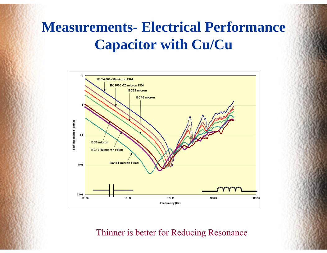
Measurements- Electrical Performance Capacitor with Cu/Cu
0.001
0.01
0.1
1
10
1E+06 1E+07 1E+08 1E+09 1E+10
Frequency (Hz)
Self
Impe
danc
e (o
hms)
ZBC-2000 -50 micron FR4
BC1000 -25 micron FR4BC24 micron
BC16 micron
BC8 micron
BC12TM micron Filled
BC16T micron Filled
Thinner is better for Reducing Resonance

Full Sheet Resonance Self Z
0.001
0.01
0.1
1
10
1E+06 1E+07 1E+08 1E+09 1E+10
Frequency (Hz)
Impe
danc
e (o
hms
FaradFlex BC24
Effect of Increased Loss on Impedance of Capacitance Material
Simulated Effect
24 μ Embedded Capacitance Material
Increased Loss due to Resistor layer makesCapacitance Material perform as if it is Thinner!
Measurements- Electrical PerformanceCapacitor

Measurements- Electrical PerformanceResistor Layer
Capacitor Material vs. FR4
Sheet Resistivities (ohm/square) 25 25 Nominal Material Tolerance +/-5% +/-5 %
MIL-STD-202-108I Load Life Cycling Test Ambient Temp: 70C Resistor Size: 0.500" X 0.050" On Cycle: 1.5 hrs Loaded: (Δ R%) @ 150mW <0.9 after 3200 hrs.) <5 Off Cycle: 1.5 hrs Unloaded: (Δ R%) <0.74 after 3200 hrs.) Length Of Test: 10000 hrs
MIL-STD-202-308 Current Noise Index in dB <-23 <-15 Voltage Applied: 5.6 Volts
MIL-STD-202-103A Temp: 40 °C
Humidity Test (Δ R%) 0.5 0.5 Relative Humidity: 95% Time: 240 hrs MIL-STD-202-304
Characteristic (RTC) PPM/°C -6.0 50 Hot Cycle: 25°, 50°,75° 125°C Cold Cycle: 25°, 0°,-25°, -55°C MIL-STD-202-107B
Thermal Shock (Δ R%) 0.2 -0.5 No of Cycles: 25 Hot Cycle Temp: 125 °C Cold Cycle Temp: -65 °C
Solder Float (Δ R%) MIL-STD-202-210D After 1 Cycle -0.4 0.5 Temp: 260°C After 5 cycles -0.6 Immersion: 20 Second Power Density (mW/mil 2) 0.45 0.15 Step-up Power Test derated at 50% Resistor size 0.020" x 0.030"
Properties NiP/CapacitorCore
NiP CoreFR-4 (control)
Remarks and Conditions
Synergistic Effect !

Resistor Sizing
L1 = W1 L2 = W2 L3 =W3R1 = 25 Ohms R2 = 25 Ohms R3 = 25 Ohms
•Shape of Resistor plus Sheet Resistivity determines theOhmic value
•Larger L vs. W increases Resistance•Operating Power determines the size of the Resistor
•Resistor size goes up as Power requirement goes up•Higher Power Density results in smaller Resistors
3L x 1WR = 75 Ohms
4L x 2WR = 50 Ohms

Performance:Thermal Stability
Buried Capacitance™ Core Standard Core
Thinner dielectric provides better heat transfer to copper

Typical Applications
Example of combined product with terminating resistorsin an existing layer.

Typical Applications
Ohmega Technologies, Inc.
4031 Elenda Street Culver City, California 90232 Phone: (310) 559 - 4400 Fax: (310) 837 - 5268Web Site: www.Ohmega.com
R3R2R1
R4R5R6R7
R8
R9
R10
R11
R12
R13
R14
R15
R16R17R18R19
hmega
Example of RC Networks in Demo PCB

NiP Thin Film Resistors
Capacitor MaterialR9
R10
R11
Resistors (R9, R10 & R11)•44 Ω nominal
Capacitance (0.6 nF)•1.2 nF/in2
Embedded R/C Example
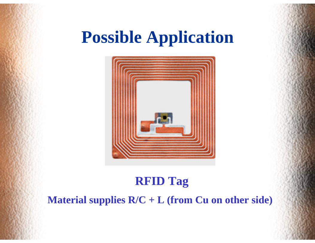
Possible Application
RFID TagMaterial supplies R/C + L (from Cu on other side)

SummaryAdvantages of Combined Embedded R/C
TechnologyElectrical Advantages
1. Improved line impedance matching2. Shorter signal paths and reduced series inductance3. Eliminate the inductive reactance of the SMT device4. Reduced cross talk, noise and EMI
PCB Design Advantages1. Increase active component density & reduced formfactors.2. Improved wireability due to elimination of via.3. Improved reliability due to elimination of solder joints.
Economic Advantages1. Elimination of discrete resistors and capacitors.2. Improved assembly yield3. Board densification and/or size reduction4. Improved Material Cost Structure

SummaryAdvantages of Combined Embedded R/C Technology
LEAD
Ultimate Lead-Free Solution!

Future Studies
• Impedance versus Frequency– Finish Testing of 25 ohm/sq Resistor Foil on 24μ
Capacitor Material– Effect of Ohm/sq on Capacitor Performance
• Resistor/Capacitor Properties on other Capacitor Substrates– Effect of Thickness and Dk
• Verify/Quantity Synergistic Effects• Investigate Unique Circuit Patterns

Conclusion• Combined R/C Material results in reliable embedded passives
on a single embedded core.• Meets all Resistor Foil Specifications.• Meets all the Buried Capacitance ™ Material Specifications. • Any PCB manufacturer capable of making Buried Resistors
and Licensed to Produce Buried Capacitance™ cores can produce the Combined R/C PCBs.
• Cost advantage of combined product due to reduced form factors, layer count and elimination of greater numbers of SMTs.
• Combining the two materials enhances the performance of each material.
• Allows unique circuit designs
Note: Buried Capacitance™ is a trademark of HSCI

For Further Information visit ourWeb Sites
www.oakmitsui.comwww.ohmega.com
Related Documents