Novel Power Electronic Device Structures for Power Conditioning Applications By Ajith Balachandran A thesis submitted for the degree of PhD. Department of Electronic & Electrical Engineering, The University of Sheffield, UK OCTOBER 2014

Welcome message from author
This document is posted to help you gain knowledge. Please leave a comment to let me know what you think about it! Share it to your friends and learn new things together.
Transcript
Novel Power Electronic Device
Structures for Power Conditioning
Applications
By
Ajith Balachandran
A thesis submitted for the degree of PhD.
Department of Electronic & Electrical Engineering,
The University of Sheffield, UK
OCTOBER 2014


ABSTRACT
Silicon MOS controlled bipolar devices are considered to be the most preferred device
technology for most low and medium voltage power applications. The economic and
environmental benefits achievable by moving to more energy efficient power semiconductor
and power conversion systems are well documented. A major factor that limits the
performance of the MOS controlled bipolar structures is the current distribution within the
device. An inhomogeneous current distribution within the device is a well known cause
current filamnetation leading to device failure. Therefore it was logical to evaluate the key
manufacturing parameters that might impact the current distribution in the device, other than
ones already discussed in available literature. The work presented in this thesis evaluates the
variation in resistivity caused due to the growth of the silicon wafer on the device
performance. It was concluded that the variation of resistivity might not impact device
performance substantially. However, the variation can cause a drift in the device
characteristics across the wafer which can then impact the power module if the devices are
not chosen properly.
The focus then moves to the design optimisation of a CIGBT structure and shows methods of
optimising the anode side of the device so as to give better performance trade off without
compromising the other characteristics of the device. The proposed anode design shows how
an existing structure can further optimise the device performance by reducing the turn off
losses of the device by about 50% while maintaining the on-state voltage. It is then shown
how the CIGBT concept can provide a short circuit withstand capability of more than 100µs,
which is higher than any MOS controller bipolar device ever reported.
The thesis also looks at various methods of optimising the cathode end of the device by the
use of a segmented P-base structure. This structure is also experimentally evaluated and the

results show that the device can improve the turn-off performance while maintaining or
improving the on-state voltage.
The final focus of the work then looks at a converter optimisation method using low voltage
silicon devices and commercially available GaN devices. The results clearly show the
dominance of GaN technology which, in the years to come, can become one of the most
favourable technologies as compared to that of their silicon counterparts. However, this
technology requires to be developed upon further with the aspect of thermal management
requiring special attention.

ACKNOWLEDGEMENTS
I would like to express my immense gratitude and thanks to the following:-
1. Professor Geraint W Jewell for his consistent and valuable support in guiding me in
my research program.
2. Professor Shankar Ekkanath Madathil under whose effective supervision I had the
opportunity to work on emerging power device technologies.
3. Dr.Mark Sweet and Dr. Keir Wilkie for their invaluable guidance during numerous
discussions regarding the set-up of my experimental system.
4. Dr. Luther-King Ngwendson for his invaluable comments and guidance.
5. The Technical Staff of the Department of Electrical and Electronics Engineering who
have helped me in several ways.
6. My fellow colleagues for their valuable help and support contributed through several
interesting discussions.
7. I would particularly like to thank my wife, my father and my mother for being
patient and supportive.
8. The Rolls Royce University Technology Centre at The University Of Sheffield, for
financial support over the period of this research.
Last but not least I thank The University of Sheffield for giving me access to such a
wonderful experience in terms of both, knowledge and work culture.

LIST OF PUBLICATIONS
1. ISPSD Conference Publication “Enhanced Short-circuit performance of 3.3kV
Clustered Insulated Gate Bipolar Transistor (CIGBT) in NPT technology with RTA
Anode.” A.Balachandran, L.Ngwendson, E.M.Sankara Narayanan, Shona Ray,
Henrique Quaresma, John Bruce.
2. IEEE – Electron Device “Performance Evaluation of 3.3-kV Planar CIGBT in NPT
Technology With RTA Anode”, A. Balachandran, M.R. Sweet, N. Luther-King and
E.M. Sankara Narayanan, Senior Member, IEEE, Shona Ray, Henrique Quaresma.
John Bruce
3. ISPS Conference Publication “Evaluation of 1.2kV segmented cathode cell design for
Trench Clustered Insulated Gate Bipolar Transistor (TCIGBT)”, A. Balachandran, L.
Ngwendson and E.M. Sankara Narayanan, Senior Member, IEEE.
4. ISPSD Conference Publication “2.4kV GaN Polarization Superjunction Schottky
Barrier Diodes on Semi-Insulating 6H-SiC Substrate”, Vineet Unni, Ajith
Balachandran, Hong Long, Mark Sweet and E. M. Sankara Narayanan, Senior
Member, IEEE
5. IEEE – Electron Devices - “Evaluation of 1.2kV segmented cathode cell design for
Trench Clustered Insulated Gate Bipolar Transistor (TCIGBT)”, A. Balachandran, L.
Ngwendson and E.M. Sankara Narayanan, Senior Member, IEEE. (Working on
reviewers comments)

LIST OF FIGURES
Figure 1-1: Efficiency of Power Plants [1.1] ....................................................................................................... 1
Figure 2-1 (a) Czochralski crystal pulling furnace, (b) Silicon Ingot [2.3] .................................................... 14
Figure 2-2: Generic IGBT Trench-Structures (a) NPT-IGBT (b) PT-IGBT ................................................ 16
Figure 2-3: Graphical interpretation of the flow of charge in an IGBT during its on-state [2.11] .............. 17
Figure 2-4: Electric field distribution of the a) PT (punch through) b) Non-punch through c) field stop
structure [2.12] ........................................................................................................................................... 19
Figure 2-5: Cross section view of the IGBT along with its leading dimensions............................................. 20
Figure 2-6: Typical chopper circuit used for simulation. ................................................................................ 21
Figure 2-7: Simulated inductive turn-off switching performance of 1.2kV IGBT. VDC=600V, I=100Amps,
τ=10µs, T=25°C .......................................................................................................................................... 22
Figure 2-8: Cross section of the multi-cell structure of the IGBT along with the variation of the drift
doping concentration in the X direction................................................................................................... 23
Figure 2-9: Variation of doping concentration along X axis for the IGBT structure shown in Figure 2-8 23
Figure 2-10: Simulated Inductive switching performance of the 11-cell structure. VDC=600V, I=100Amps,
Carrier lifetime (τ) =10us, T=25°C ........................................................................................................... 24
Figure 2-11: Current distributions across the 11-Cell structure during (a) turn-off condition (b) the on-
state condition ............................................................................................................................................ 25
Figure 2-12: Variation of threshold voltage and saturation current density of the device with substrate
resistivity, Drift depth = 120μm, baseline for variation = 1×10¹⁴
cm-3
, Carrier lifetime (τ) =10us ..... 26
Figure 2-13: Variation of resistivity on the on-state voltage, Drift depth = 120μm, 0% variation = 1e14 cm-
3, Carrier lifetime (τ) =10us ....................................................................................................................... 26
Figure 2-14: Variation of resistivity on the breakdown voltage of the device, Drift depth = 120μm, 0%
variation = 1x10¹⁴
cm-3
, Carrier lifetime (τ) =10us .................................................................................. 27
Figure 2-15: Variation of resistivity on the turn-off losses on the device, Drift depth = 120μm, 0%
variation=1x10¹⁴
cm-3
, Carrier lifetime (τ) =10us .................................................................................... 28
Figure 3-1: A schematic of the NPT-CIGBT cell along with its equivalent circuit. ...................................... 32
Figure 3-2: A fabricated wafer showing devices rated 50A and 6A. The layout contains several CIGBT
and IGBT designs for comparison ............................................................................................................ 34

Figure 3-3: SRP plots for the 3.3kV NPT anode structure of 1×10¹²
@ 40keV ............................................. 35
Figure 3-4 : Simulated electric field profile across the 3.3kV NPT-CIGBT, Anode Voltage=3.3kV, Drift
depth=500μm .............................................................................................................................................. 36
Figure 3-5: Typical experimental CIGBT on-state I (V) at 25°C and 125°C, Vg=+15V .............................. 37
Figure 3-6: Experimentally measured CIGBT current saturation characteristics Vth = 5.5V, Tj= 25°C .. 38
Figure 3-7: Simulated carrier density profile within the CIGBT compared with IGBT at JA = 50Acm-2
.. 38
Figure 3-8: Schematic of the cathode cells showing the N-WELL and P-base circular and square designs
in CIGBT .................................................................................................................................................... 39
Figure 3-9: Experimental results on the influence of N-WELL dose (Nw1 (6.9e13) > Nw2 (6.7e13) > Nw3
(6.5e13)) on the on-state voltage Vce(sat) and saturation current density of CIGBT at 25°C ............ 40
Figure 3-10: Simulated carrier density comparison of the 3.3kV CIGBT structure with variation of the N-
WELL implant dose (Nw1 (6.9e13) > Nw2 (6.7e13) > Nw3 (6.5e13)) .................................................... 41
Figure 3-11: Simulated results showing the Influence of N-WELL dose (Nw1 (6.9e13) > Nw2 (6.7e13) >
Nw3 (6.5e13)) on the self-clamping voltage of the CIGBT at 25°C........................................................ 42
Figure 3-12: Typical chopper circuit used for testing...................................................................................... 43
Figure 3-13: Typical measured CIGBT turn-off curves at 25°C (Rg = 22ohm, Vdd=1800V) ..................... 43
Figure 3-14: Comparison of experimental NPT-CIGBT and IGBT trade-off curves at 25°C.
A1>A2>A3>A4, Rg = 22Ω, Vdd = 1800V................................................................................................. 44
Figure 3-15: Simulated CIGBT current flow during turn-off showing holes flowing through the depleted
N-WELL regions ........................................................................................................................................ 45
Figure 3-16: Typically measured CIGBT turn-off at 25°C (Rg = 100ohm, Vdd=1650V) for Vg=+15V ..... 45
Figure 3-17: Test Circuit used to study the CIGBT behaviour under UIS.................................................... 46
Figure 3-18: Anode current and voltage expected waveforms under UIS ..................................................... 47
Figure 3-19: Typically measured UIS waveforms for CIGBT at 25°C (Rg = 100ohm, Vg=+15 to 0) ......... 47
Figure 3-20: Measured UIS waveforms for CIGBT at 25°C (Vanode=400V, Rg = 100ohm, Vg=+15 to 0) 48
Figure 3-21: Experimental setup used to evaluate the short-circuit performance of the device.................. 49
Figure 3-22: Typically measured CIGBT Short-circuit waveforms at 25oC and 125
oC (Rg = 22ohm,
Vdd=1800V) for a 6A rated device Vg=+15V .......................................................................................... 50
Figure 3-23: Maximum measured CIGBT Short-circuit waveforms at 25oC (Rg = 22ohm, Vdd=1800V)
Vg=+15V ..................................................................................................................................................... 51

Figure 3-24: Typically measured CIGBT Short-circuit waveforms with variation of gate resistance at
25oC (Vdd=1800V) ..................................................................................................................................... 52
Figure 4-1: Schematic structure of a p-i-n diode ............................................................................................. 56
Figure 4-2: Change of stored carrier profile with electron injection efficiency ............................................ 57
Figure 4-3 Schematic cross section of a conventional TCIGBT with its equivalent circuit ......................... 58
Figure 4-4: The various implementation of the TCIGBT structure with cell spacing (CS) (a) Type A:
Segmented P-Base (b) Type B: Segmented P-Base with PMOS Gates, (c) Type C: Segmented P-Base
with deep PMOS and deep NMOS gates.................................................................................................. 59
Figure 4-5: The doping concentration across the CIGBT structures (cutline taken along A-A’) ............... 60
Figure 4-6: Typical Breakdown characteristics of the TCIGBT structures .................................................. 61
Figure 4-7: Typical I-V characteristics for 1.2kV TCIGBT Structures Tj=25ºC ......................................... 61
Figure 4-8: Variation of on-state voltage and turn-off losses with cell-spacing (CS) in TCIGBT with
Segmented P-base....................................................................................................................................... 63
Figure 4-9: Simulated I-V Characteristics showing current saturation with variation of cell-spacing (CS)
for TCIGBT with Segmented P-base........................................................................................................ 63
Figure 4-10: Simulated variation of on-state voltage with PMOS trench width for TCIGBT structures
with cell spacing (CS) =5µm ...................................................................................................................... 64
Figure 4-11: Simulated electron carrier density comparison of the TCIGBT structures in their on-state
with variation of the PMOS trench gates ................................................................................................. 65
Figure 4-12: Variation of turn-off losses with PMOS trench width for TCIGBT structures with cell
spacing (CS) =5µm ..................................................................................................................................... 66
Figure 4-13: Mask Layout of the TCIGBT structure showing the ladder layout of the cathode side ......... 67
Figure 4-14: Influence of variation of the PMOS trench width on the electro thermal short-circuit
performance of the device, cell spacing=5μm, V=600V, Vg=±15V and τ =20μs ................................... 67
Figure 4-15: Variation of on-state voltage and turn-off losses with cell-spacing (CS) for the Type B
structure...................................................................................................................................................... 68
Figure 4-16: Typical circuit used to evaluate the short-circuit performance of the TCIGBT ..................... 69
Figure 4-17: Influence of cell spacing (CS) on the electro thermal short circuit performance of the
segmented P-Base TCIGBT structure, V=600V, Vg=±15V and τ =20μs .............................................. 70

Figure 4-18: Predicted current flow lines in the segmented P-Base TCIGBT structure with PMOS trench
gates ............................................................................................................................................................. 71
Figure 4-19: Predicted current flow lines in the segmented P-Base TCIGBT structures with deep NMOS
and PMOS trench gates ............................................................................................................................. 71
Figure 4-20: Electron carrier density of the various TCIGBT structures in their on-state along A-A’ ..... 72
Figure 4-21: Comparison of Eoff-Vce(sat) trade-off for conventional and Segmented P-base Structures at
Tj=125ºC , V=600V, Rg=22Ω, Vg=±15V and τ =20μs, Lstray=100nH .................................................. 73
Figure 4-22: Comparison of Eoff-Vce(sat) trade-off for conventional and the Segmented P-base
Structures at Tj=25ºC , V=600V, Rg=22Ω, Vg=±15V and τ =20μs, Lstray=100nH ............................. 73
Figure 4-23: The cross section schematic of the TCIGBT structure .............................................................. 75
Figure 4-24: Mask Layout of a TCIGBT with Segmented P-Base and PMOS Gates ................................... 76
Figure 4-25: TCIGBT devices assembled on a ceramic substrate .................................................................. 77
Figure 4-26: Typical experimental CIGBT on-state I(V) at 25ºC Vg=15V.................................................... 77
Figure 4-27: Typical experimental TCIGBT on-state I(V) at 125ºC Vg=15V ............................................... 78
Figure 4-28: Typically measured current saturation characteristics for TCIGBT structures Tj= 25°C and
125°C ........................................................................................................................................................... 79
Figure 4-29: A schematic diagram showing the equivalent capacitance of the device ................................. 79
Figure 4-30: Input capacitance measurement for the TCIGBT structures ................................................... 80
Figure 4-31: Measured Output and Transfer capacitance for the TCIGBT structures ............................... 81
Figure 4-32: Comparison of performance trade-off for the TCIGBT structures Vce=600V, Ic= 10Amps,
Vge=+15V/-15V, Tj=25ºC .......................................................................................................................... 82
Figure 5-1: Expected development trends for power converters [5.2] ........................................................... 85
Figure 5-2: Application range of discrete power semiconductor device technologies in Silicon [5.5] ......... 90
Figure 5-3: Structure of a Vertical MOSFET/ Power MOSFET.................................................................... 91
Figure 5-4: Components of Rds(on) in a Vertical MOSFET .......................................................................... 92
Figure 5-5: The specific on resistance (RDS(ON-SP)) of MOSFETs with increase in their voltage ratings [5.2]
..................................................................................................................................................................... 93
Figure 5-6: Basic Structure of a Lateral MOSFET ......................................................................................... 94
Figure 5-7: Ron*A relation with designed blocking voltage of Si, SiC and GaN-Mosfet and JFET devices
as well as for bipolar IGBT devices [5.8] ................................................................................................. 95

Figure 5-8: A typical AlGaN/GaN HEMT structure with three metal-semiconductor contacts ................. 96
Figure 5-9: Structure of an enhancement mode GaN Power transistor [5.17] .............................................. 97
Figure 5-10: General arrangement of 3-Phase 2-Level voltage source converter ......................................... 99
Figure 5-11: Cascaded H-Bridge Multilevel Topology (Single phase output) [5.27] .................................. 104
Figure 5-12: General arrangement of a diode clamped multilevel converter (Single phase output) [5.27]
................................................................................................................................................................... 104
Figure 5-13: General arrangement of a flying capacitor multilevel converter (Single phase output) [5.27]
................................................................................................................................................................... 105
Figure 5-14: Switching figure of merit of Silicon MOSFETs for different voltage ratings ........................ 106
Figure 5-15: Variation of conduction losses in a single phase with number of levels (Silicon) .................. 108
Figure 5-16: Switching loss of a single H-Bridge ........................................................................................... 110
Figure 5-17: Total switching loss of the converter with number of levels.................................................... 110
Figure 5-18: Total losses in the power converter with number of levels ...................................................... 112
Figure 5-19: Variation of conduction losses with number of levels .............................................................. 113
Figure 5-20: Variation of GaN converter switching loss with frequency ..................................................... 114
Figure 5-21: Total losses converter with variation of switching frequency ................................................. 115
Figure 5-22: Comparison of switching losses and conduction losses ............................................................ 115
Figure 5-23: Comparison of GaN and Silicon devices in a multilevel converter ......................................... 116
Figure 5-24: The flip chip design used for the GaN devices .......................................................................... 117
Figure 5-25: The general pad layout for the EPC devices ............................................................................. 118
Figure 5-26: PCB Layout for the initial testing of GaN devices ................................................................... 118
Figure 5-27: Measured I-V characteristics of GaN and Silicon Devices ...................................................... 119
Figure 5-28: Measured on-state comparison at full enhancement of the channel ....................................... 120
Figure 5-29: Measured threshold voltage comparison of GaN and Silicon Devices ................................... 120
Figure 5-30: Experimental Turn-off switching waveforms of GaN EPC1011 and Silicon Devices
(IRL3215PbF)........................................................................................................................................... 121
Figure 5-31: Comparison of Turn-off losses and on-state voltage of the devices at V=1/2BV, Rg=22Ω,
Vg=5(GaN) and ±15 V(Silicon) ............................................................................................................... 122
Figure 5-32: Measured short Circuit Performance of GaN devices at Rg=22Ω, T=250C and Vg=5V,
VDC=60V.................................................................................................................................................. 123

Figure 5-33: Short Circuit Performance of Silicon devices at Rg=22Ω, T=250C and Vg=15V, VDC=75V
................................................................................................................................................................... 123
Figure 6-1: Block diagram of the loss estimation model ............................................................................... 128
Figure 6-2: Carrier and reference signals for 2 level converter using phase shifted PWM ....................... 130
Figure 6-3: Simulink model for single phase 2-level converter along with loss estimation block .............. 130
Figure 6-4: Simulink Model for the loss estimation block............................................................................. 131
Figure 6-5: Simulink model for the device loss estimation block ................................................................. 132
Figure 6-6: Simulink model for the diode loss estimation block ................................................................... 133
Figure 6-7: Data used to estimate the turn-on losses of the converter at 2-Level Silicon based converter at
different current and temperature of operation.................................................................................... 134
Figure 6-8: Data used to estimate the turn-off losses of the converter at 2-Level Silicon based converter at
different current and temperature of operation.................................................................................... 134
Figure 6-9: Data used to measure the conduction losses of the 2-Level Silicon based converter at different
temperature and operating currents ...................................................................................................... 135
Figure 6-10: Output current and voltage waveforms of the two level converter fundamental frequency
=400Hz, Carrier frequency=10 kHz ....................................................................................................... 136
Figure 6-11: Estimated losses for the top device in one half of the H-Bridge configuration ...................... 137
Figure 6-12: Variation of junction temperature with converter operation ................................................. 137
Figure 6-13: Variation of switching losses with carrier frequency ............................................................... 138
Figure 6-14: Total conduction loss of converter with number of levels ....................................................... 139
Figure 6-15: Total Losses of the converter with number of levels ................................................................ 139
Figure 6-16: Total losses of converter GaN vs Silicon comparison (300V, 50A) ......................................... 140
Figure 6-17: Loss comparison of Silicon and GaN devices for under an RL load ...................................... 141
Figure 6-18: Output current and voltage waveforms of the 7-level converter, Fsw=10 kHz ..................... 141
Figure 6-19: Output voltage of a 2-level, 7-level and 31-Level converter at a switching frequency of 10
kHz and 300V/50Amps ............................................................................................................................ 142
Figure 6-20: Total harmonic distortion vs number of levels ......................................................................... 144
Figure 6-21: Deposition of solder on the PCB boards ................................................................................... 145
Figure 6-22: Picture of device post assembly.................................................................................................. 145
Figure 6-23: Failure of Plug-in Modules due to short between source and drain pads .............................. 146

Figure 6-24: Block diagram of the H-Bridge Circuit..................................................................................... 147
Figure 6-25: Drive circuit for the top device in one half of the H-bridge .................................................... 148
Figure 6-26: Completed H-Bridge Circuit in a 5-phase converter arrangement ........................................ 149
Figure 6-27: Probe measurement setup for the EPC1010 die using the Textronix-371B ........................... 150
Figure 6-28: Test setup for assembled device post assembly ........................................................................ 150
Figure 6-29: Pad Layout for EPC 1010 GaN Transistor (200V/12A) [6.14] ................................................ 151
Figure 6-30: Circuit used to drive the GaN devices in a chopper circuit ..................................................... 152
Figure 6-31: Layout circuit for the switching test setup, Top Copper (Silk), Bottom Copper (Blue), Yellow
(Board Edge) ............................................................................................................................................ 152
Figure 6-32: Test setup used to measure device switching and short-circuit performance........................ 153
Figure 6-33: Test setup for the 5-Level converter .......................................................................................... 155
Figure 6-34: Measured Leakage current of the EPC1010 device as a function of anode voltage for various
drain -source terminals (compared against 200V/12A Silicon Device) ............................................... 156
Figure 6-35: Leakage characteristics of the device post device assembly .................................................... 156
Figure 6-36: Typical I-V characteristics of EPC1010 GaN Devices ............................................................. 158
Figure 6-37: Typical forward characteristics of the body diode with drain-source current ...................... 158
Figure 6-38: Structure of MOSFET showing body diode. ............................................................................ 159
Figure 6-39: Measured turn-off performance of the EPC1011 GaN devices .............................................. 160
Figure 6-40: Measured turn-on and turn-off losses of EPC1011 GaN devices with load current ............. 160
Figure 6-41: Measured variation in turn-off losses with Gate resistance .................................................... 161
Figure 6-42: Measured output voltage and current waveforms of a single H-Bridge using EPC1011
devices (Switching frequency=10 kHz, DC link 60V) ........................................................................... 162
Figure 6-43: Measured efficiency of the H-Bridge circuit using EPC1011 devices (Vout=60V, Iout=1A) 162
Figure 6-44: Measured case temperature of the device with switching frequency of 10 kHz, Operating
voltage=60V and 1Amp ........................................................................................................................... 163
Figure 6-45 Total losses in a H-Bridge arrangment., Fsw=10kz, output current -12Amps, Vout=75V .... 164
Figure 6-46: Case temperature of the device in the H-Bridge arrangment., Fsw=10kz, output current -
12Amps, Vout=75V .................................................................................................................................. 164

LIST OF TABLES
Table 2-1: Material properties of Silicon [2.1] [2.2]......................................................................................... 12
Table 2-2: Simulated static characteristics of 1.2kV Trench-IGBT ............................................................... 20
Table 4-1: Proposed process for the 1.2kV segmented P-base TCIGBT structures ..................................... 74
Table 5-1: Key methods used to allow reduction in power converter weight and size ................................ 88
Table 5-2: Typical Power device characteristics [5.4] ..................................................................................... 89
Table 5-3: Material properties of GaN, SiC and Silicon [5.22] ....................................................................... 98
Table 5-4: A high level comparison of the basic multi-level converter arrangements ................................ 103
Table 5-5: Devices considered as a part of this study .................................................................................... 106
Table 5-6: Ron comparison of series connected devices with number of levels........................................... 107
Table 5-7: Commercially available GaN devices used for comparison ........................................................ 112
Table 5-8: Ron comparison for series connected devices with number of levels ......................................... 113
Table 6-1: Measured resistance of the Load Bank......................................................................................... 154

TABLE OF CONTENTS
CHAPTER ONE ................................................................................................................................................. 1
1.1. INTRODUCTION ............................................................................................................................... 1
1.2. POWER ELECTRONICS ................................................................................................................. 2
1.2.1. POWER CONVERTERS .................................................................................................................. 3
1.2.2. POWER SEMICONDUCTORS DEVICES ................................................................................... 3
1.3. THESIS STRUCTURE ...................................................................................................................... 5
1.4. REFERENCES .................................................................................................................................. 10
CHAPTER TWO .............................................................................................................................................. 12
2.1 INTRODUCTION ............................................................................................................................... 12
2.2 INSULATED GATE BIPOLAR JUNCTION TRANSISTORS ...................................................... 15
2.2.1 DEVICE OPERATION ....................................................................................................................... 16
2.2.2 DRIFT ENGINEERING ..................................................................................................................... 18
2.3 IMPACT OF VARIATION OF DOPING CONCENTRATION .................................................... 19
2.3.1 HALF CELL DEVICE STRUCTURE .............................................................................................. 19
2.3.1.1 SIMULATION RESULTS .................................................................................................................. 20
2.3.2 MULTI-CELL DEVICE STRUCTURE ............................................................................................ 22
2.3.2.1 SIMULATION RESULTS .................................................................................................................. 24
2.3.3 MAXIMUM ACCEPTABLE VARIATION...................................................................................... 25
2.4 CONCLUSION .................................................................................................................................... 28
2.5 REFERENCES .................................................................................................................................... 30

CHAPTER THREE ......................................................................................................................................... 31
3.1 INTRODUCTION ............................................................................................................................. 31
3.2 TRANSPARENT ANODE DESIGN ............................................................................................. 31
3.3 DEVICE STRUCTURE AND OPERATION .............................................................................. 33
3.4 EXPERIMENTAL RESULTS ........................................................................................................ 34
3.4.1 FORWARD BLOCKING VOLTAGE .......................................................................................... 35
3.4.2 ON-STATE PERFORMANCE ....................................................................................................... 36
3.4.2.1 INFLUENCE OF CATHODE CELL GEOMETRY ................................................................. 39
3.4.2.2 INFLUENCE OF N-WELL IMPLANT DOSE .......................................................................... 40
3.5 CLAMPED INDUCTIVE SWITCHING PERFORMANCE ................................................... 42
3.6 UNCLAMPED INDUCTIVE SWITCHING PERFORMANCE ............................................ 46
3.7 SHORT CIRCUIT PERFORMANCE .......................................................................................... 49
3.7.1 INFLUENCE OF GATE RESISTANCE ..................................................................................... 51
3.8 CONCLUSION .................................................................................................................................. 52
3.9 REFERENCES .................................................................................................................................. 54
CHAPTER FOUR ............................................................................................................................................ 55
4.1. INTRODUCTION ............................................................................................................................. 55
4.2. ELECTRON INJECTION EFFICIENCY .................................................................................. 55
4.3. DEVICE STRUCTURE AND OPERATION .............................................................................. 58
4.4. INFLUENCE OF CELL SPACING ON SEGMENTED P-BASE TCIGBT ....................... 62
4.5. INFLUENCE OF PMOS TRENCH GATE ................................................................................. 64
4.5.1. ON-STATE PERFORMANCE ....................................................................................................... 64
4.5.2. INDUCTIVE SWITCHING PERFORMANCE ......................................................................... 65

4.5.3. ELECTROTHERMAL SHORT CIRCUIT PERFORMANCE .............................................. 66
4.6. INFLUENCE OF CELL SPACING ON TCIGBT WITH PMOS GATES .......................... 68
4.6.1. ON-STATE PERFORMANCE ....................................................................................................... 68
4.6.2. ELECTROTHERMAL SHORT CIRCUIT PERFORMANCE .............................................. 68
4.7. INFLUENCE OF DEEP NMOS AND PMOS TRENCH GATES .......................................... 70
4.7.1. PERFORMANCE TRADE OFF .................................................................................................... 72
4.8. DEVICE FABRICATION ............................................................................................................... 74
4.9. EXPERIMENTAL RESULTS ........................................................................................................ 76
4.9.1. MEASURED ON-STATE PERFORMANCE ............................................................................. 77
4.9.2. CAPACITANCE MEASUREMENT............................................................................................. 79
4.9.3. PERFORMANCE TRADE OFF .................................................................................................... 81
4.10. CONCLUSIONS ................................................................................................................................ 82
4.11. REFERENCES .................................................................................................................................. 84
CHAPTER FIVE .............................................................................................................................................. 85
5.1. INTRODUCTION ............................................................................................................................. 85
5.2. CANDIDATE SEMICONDUCTOR DEVICE TECHNOLOGY............................................ 88
5.2.1. SILICON BASED DEVICE TECHNOLOGY ............................................................................ 88
5.2.1.1. SILICON POWER MOSFETS ...................................................................................................... 90
5.2.2. GALLIUM NITRIDE (GAN) BASED DEVICE TECHNOLOGY ........................................ 94
5.2.3. SILICON CARBIDE BASED DEVICE TECHNOLOGY ....................................................... 98
5.3. POWER CONVERTER TOPOLOGIES ..................................................................................... 99
5.3.1. MULTILEVEL CONVERTERS .................................................................................................. 101
5.4. LOSS ANALYSIS OF LOW VOLTAGE SILICON DEVICES ........................................... 105

5.4.1. EVALUATION OF CONDUCTION LOSSES ......................................................................... 108
5.4.2. EVALUATION OF SWITCHING LOSSES ............................................................................. 109
5.4.3. TOTAL LOSSES OF LOW VOLTAGE SILICON DEVICES ............................................ 111
5.5. LOSS ANALYSIS OF GAN DEVICES ..................................................................................... 112
5.5.1. EVALUATION OF CONDUCTION LOSSES ......................................................................... 113
5.5.2. EVALUATION OF SWITCHING LOSSES ............................................................................. 114
5.5.3. TOTAL LOSSES OF THE GAN DEVICES ............................................................................. 115
5.5.4. COMPARISON OF GAN AND SILICON DEVICES ............................................................ 116
5.6. EXPERIMENTAL EVALUATION OF SI AND GAN DEVICES ....................................... 117
5.6.1. STATIC CHARACTERISTICS .................................................................................................. 119
5.6.2. DYNAMIC CHARACTERISATION ......................................................................................... 121
5.6.3. SHORT CIRCUIT PERFORMANCE TEST ............................................................................ 122
5.7. CONCLUSION ................................................................................................................................ 124
5.8. REFERENCES ................................................................................................................................ 125
CHAPTER SIX ............................................................................................................................................... 127
6.1. INTRODUCTION ........................................................................................................................... 127
6.2. CONVERTER LOSS ANALYSIS ............................................................................................... 127
6.2.1. DEVICE PARAMETER ESTIMATION FOR LOOK UP TABLE .................................... 133
6.2.2. SIMULATION RESULTS ............................................................................................................ 135
6.2.2.1. LOSS COMPARISON OF SILICON AND GAN BASED CONVERTERS ...................... 140
6.2.3. IMPACT ON PASSIVE FILTER ................................................................................................ 142
6.2.3.1. HARMONIC ANALYSIS OF THE OUTPUT VOLTAGE ................................................... 143
6.3. HARDWARE PROTOTYPE DEVELOPMENT ..................................................................... 144

6.3.1. DEVELOPMENT OF PLUG-IN-MODULES .......................................................................... 144
6.3.2. DEVELOPMENT OF THE H-BRIDGE CIRCUIT ................................................................ 146
6.3.3. DEVELOPMENT OF THE 5-LEVEL CONVERTER CIRCUIT ....................................... 148
6.4. TEST SETUP ................................................................................................................................... 150
6.4.1. TEST SETUP FOR STATIC DEVICE CHARACTERISTICS ........................................... 150
6.4.2. TEST SETUP FOR SWITCHING LOSS MEASUREMENTS ............................................. 151
6.4.3. TEST SETUP FOR CONVERTER LOSS MEASUREMENTS ........................................... 154
6.5. EXPERIMENTAL RESULTS ...................................................................................................... 155
6.5.1. FORWARD BREAKDOWN VOLTAGE MEASUREMENTS ............................................. 155
6.5.2. STATIC MEASUREMENTS ........................................................................................................ 157
6.5.3. SWITCHING LOSS MEASUREMENTS .................................................................................. 159
6.5.4. CONVERTER LOSS MEASUREMENTS ................................................................................ 161
6.6. CONCLUSION ................................................................................................................................ 165
6.7. REFERENCES ................................................................................................................................ 167
CHAPTER SEVEN ........................................................................................................................................ 168
7.1. CONCLUSION .................................................................................................................................. 168
7.2. REFERENCES .................................................................................................................................. 172
APPENDIX A .................................................................................................................................................. 173
APPENDIX B .................................................................................................................................................. 188
APPENDIX C .................................................................................................................................................. 200
APPENDIX D .................................................................................................................................................. 204

P a g e | 1
CHAPTER ONE
Chapter 1
1.1. INTRODUCTION
The major motivation behind the power electronics industry is to facilitate cost reduction in
the power generated, transmitted and distributed while maintaining stability of the power
system for various different applications. It is observed that the efficiency for most power
plants is less than 50% as shown in Figure 1-1 [1.1] [1.2].
Figure 1-1: Efficiency of Power Plants [1.1]
This inefficiencies is due to the process of converting energy from fuel stock (such as coal,
gas, uranium etc...) into mechanical energy and finally into electrical energy via the
generators. Once converted into electrical energy this needs to be transmitted and distributed
to various users. In most cases the losses in transmission and distribution of electrical energy

P a g e | 2
account for 6% to 8% of the overall losses [1.3]. If this trend continues, along with an
increase in the power demand as predicted by [1.4] [1.5], the net result will be an increase in
associated costs.
In addition to the above, as the power demand and losses keep increasing, more natural
resources will get consumed resulting in an increase in the carbon footprint. The carbon
footprint provides a direct relation to the amount of greenhouse gases emitted from our day to
day activities. This is usually composed of two parts [1.1] .
1. The primary footprint: A measure of the direct emission of CO2 from burning fossil
fuels including domestic energy consumption and transportation.
2. The secondary footprint: It is a measure of the indirect CO2 emission caused due to
the lifecycle of the products we use (manufacturing to disposal), and forms a direct
relation to supply and demand.
The long term effect of the increase of greenhouse gases has been well documented and their
effects are observed in our day to day lives (i.e., change in ocean salinity, wind patterns,
increased precipitation and intense tropical cyclones, tsunamis etc...). Although there is a
great deal of effort being directed towards developing and discovering renewable sources of
energy with an aim to reduce an impact on the environment [1.5], these efforts would be
undermined if a solution to minimise the losses in the rest of the system is not arrived at. It
would be therefore quite logical to conclude that it is imperative that we move to newer
methods of power production/distribution and conversion based on the development and use
of more energy efficient and, consequently, cost effective devices
1.2. POWER ELECTRONICS
The field of power electronics involves the control, conversion and conditioning of electrical
power. Hence, the application range of power electronics is from a few milliwatts (mobile
phones) to hundreds of megawatts (Transmission systems). Power electronics is based on

P a g e | 3
providing an average equivalent power to the system while operating the devices in their
switching state. Control and conditioning methods are then adopted to ensure that the
efficiency and reliability of system is not compromised at different operating points.
1.2.1. POWER CONVERTERS
Industrial applications always demand power conversion from one form to the other. Power
electronic converters have been proven to process electrical power in a controlled manner as
required by the load or the specific industrial process. In their most basic form, power
electronic converters can be divided into the following categories: AC to DC (Rectifiers), DC
to DC (Choppers), DC to AC (Inverters) and AC to AC (AC controllers/ Frequency
changers). AC to AC power conversion normally requires a DC interlink with the exception
of Matrix / Cyclo converters. During the 1940’s, power conversion usually necessitated the
use of expensive rotating machines. Hence these were rarely employed. With the
development of the Silicon Control Rectifiers (SCR) technology in the late 1950’s, power
conversion can been more controlled. The development of semiconductor devices over the
past decade has further made power electronic converters more economical, reliable,
flexible and completely controllable. Hence their applications are myriad. In a variable
speed drive, the power and speed rating are now no longer governed by
semiconductor devices but by the performance of the electric motor [1.6]. Power electronic
converters have now become an integral part of the electric drive system.
1.2.2. POWER SEMICONDUCTORS DEVICES
One of the most important elements of a power electronic system is the power semiconductor
device where the term semiconductor applies to all solid state materials which, due to their
band structure, have a small or large number of electrons which are freely available for
conduction. Over the past decade silicon based semiconductor device technology has matured

P a g e | 4
at an exponential rate. This follows from the increased reliability and performance benefits
expected by the power electronic conversion stages in aerospace, automotive and various
other applications. Insulated gate bipolar transistors (IGBT) are currently the most widely
favoured silicon based power devices used in the industry; this is due to their MOS gate
control, low on state and switching losses. In addition to this, the IGBTs also offer a
relatively easy parallel connection with preferable temperature coefficients and a large safe
operating area. A lot of attention has been focused on improving the performance of these
IGBTs in terms of their on-state performance and switching speeds to improve the
gravimetric power density of the power converters. Currently, in high power applications,
Trench IGBTs are more favoured over the planar counterparts as they have the ability to
boost the carrier density in the device through an increase in the active cell density per unit
area. This is particularly helpful in improving the on-state performance of the device.
However, they tend to lack the dynamic response required during the short circuit phase as
compared to planar devices. The various advantages and disadvantages of the planar and
trench technologies have been highlighted in [1.7] [1.8] [1.9].
In addition to the trench gate structures, various other methods have been discussed in
available literature to improve the performance of IGBTs. One method actively employed by
semiconductor manufacturers to improve on-state performance of IGBTs, is to boost the hole
concentration at the cathode side of the device. The improvement in the hole concentration
demands more electrons to be injected into the active silicon area, thus allowing for a higher
conductivity modulation in the device. This method is commonly referred to as the hole pile
up effect or the electron injection enhancement. Technologies such as the Injection-
Enhanced Gate Transistor (IEGT) [1.10] [1.11] are reported to enhance the injection of
electrons using a hole pile-up effect, but they result in instabilities as a result of charge
imbalance at the gate [1.10]. Carrier Stored Trench-Gate Bipolar Transistor (CSTBT) and

P a g e | 5
High-Conductivity IGBT (HiGT) devices use an n-type barrier layer to achieve lower on-
state voltages with similar saturation characteristics to that of conventional IGBTs [1.12]
[1.13]. However, the concentration of n-type barrier layer needs to be carefully controlled in
terms of the implant and drive condition so that the expansion of depletion region does not
increase the turn-off losses of the device or degrade the forward blocking performance.
The other method to improve the on-state performance of the MOS controlled bipolar power
devices is to have a thyristor mode of operation. MOS Controlled Thyristor (MCT) [1.14],
Emitter Switched Thyristor (EST) and Clustered Insulated Gate Bipolar Transistor (CIGBTs)
[1.15] are devices that show a thyristor mode of operation in their on-state. However, of
these, the planar gate CIGBT and trench gate CIGBT structures are the only MOS controlled
thyristor devices which have been experimentally proven to show excellent current saturation
characteristics even at high gate voltages due to their inherent self-clamping capability [1.15].
Hence further development of the CIGBT technology has been discussed as part of this
thesis.
Wide bang gap devices have also made remarkable progress in the last few years and
these devices are now challenging the Silicon market due to their improved material
properties. As these device technologies improve by reducing losses, the cost of device
fabrication and operation needs to be simultaneously reduced.
1.3. THESIS STRUCTURE
The work presented in this thesis contains an investigation into the methods by which the
semiconductor device performance can be improved with an aim to reduce the overall losses
in the power conversion system. The types of device technologies discussed and evaluated in
this thesis include Silicon MOSFETs, IGBT, CIGBT and GaN HEMT devices. The
performance improvement methods suggested in literature usually involve a trade-off of
device characteristics with one another. Therefore an investigation into new device

P a g e | 6
technologies and structures is deemed necessary such that the performance trade-off can be
avoided or be improved.
The work presented in this thesis initially looks at the drift engineering of the device with a
focus on IGBT structures. The variation of substrate resistivity is investigated using a
SENTARUS DEVICE simulator and the results clearly show the variation will not cause any
significant impact on device on-state and turn-off performance of the IGBT.
The thesis then covers the development and optimisation of the 3.3kV CIGBT devices. The
anode and cathode optimisation of the structure is done using commercially available
simulation packages such as MEDICI and TSUPREM IV. The devices are then designed in
TCAD SENTARUS–IC and fabricated in Semifab, once the fabrication process was
baselined. The fabricated devices were then packaged via a third party supplier in TO-247
package and experimentally evaluated using industrial standard techniques at The University
Of Sheffield. These devices are then compared with other commercially available IGBTs in
order to evaluate the performance benefits. The work presented here also builds on the work
done by Dr.Mark Sweet and Dr. Luther-King Ngwendson [1.16]. The results presented show
the CIGBT with RTA anode reduces the turn-off losses of the device by more than 50% as
compared to the previous technology demonstrated [1.16]. It is further shows that the devices
provide a short circuit capability of more than 100µs which is 10 times higher than
commercially available devices.
The thesis work then focuses on the cathode optimisation of CIGBT structures using a
segmented P-base concept for a 1.2kV CIGBT device. All segmented P-base devices
structures were simulated using MEDICI and TSUPREM IV and the preferred device
structures were designed in TCAD SENTARUS-IC. These devices were then fabricated in
collaboration with in industrial partner. Finally the devices were then assembled in The

P a g e | 7
Sheffield of University on a metallised substrate for further experimental evaluation. The
results presented for this work clearly show that the turn-off losses of the device can be
reduced by 23% while maintaining its on-state performance. In addition to this the structure
also enhances the short circuit performance of the device due to the reduction of active cells
per unit area. Although the work presented here is based on a 1.2kV device. The work can be
applied to any voltage rating.
The remaining part of the thesis looks at a converter design from a device point of view. The
device selection is discussed with aim to reduce the overall losses. A number of prototypes
are then built to evaluate the 1st generation GaN device. Various challenges were encountered
during this process. This included the assembly of the dies, the reduction of the stray
inductance in the circuit and technology issues such as current collapse in order to switch the
device within the safe operating area. These devices were experimentally evaluated in a
chopper circuit and an H-Bridge arrangement. The gate drive circuit and the switching
algorithms were developed during the process of testing the devices. The experimental and
simulation results presented for this work clearly show that although GaN devices can
provide a far better performance as compared to Silicon devices. However, the technological
advancement needed to make this device feasible for high power converter applications are
far too many.
The work outlined above in structured into the thesis in the following manner.
Chapter 1: Introduction.
Chapter 2: Reviewing the challenges encountered in the fabrication of solid state
semiconductor devices such as IGBTs and evaluating its impacts on the device
performance.

P a g e | 8
Novelty- The chapter provides simulation results to justify the amount of
substrate variability that can be allowed for device fabrication without
compromising device performance.
Chapter 3: Performance evaluation of the CIGBT with planar gates in Non Punch
Through Technology (NPT) with Rapid thermal annealing (RTA) of anode.
Novelty- The chapter provides simulation and experimental results to support
the use of RTA process in CIGBT structures and shows how the device
performance can be further improved. The results for this work are published
in ISPSD and IEEE Electron devices (Publication 1 and 2).
Chapter 4: Novel TCIGBT structures to improve the short circuit capability of device
while maintaining the on-state and switching performance.
Novelty- This chapter provides simulation and experimental results to support
the use of Segmented P-base structures in TCIGBT and shows how the device
performance can be improved while maintaining the Vce-Eoff trade-off. The
results from this work are published in ISPS and are being submitted for IEEE
Electron devices also (Publication 3 and 5).
Chapter 5, 6: Investigating and evaluating the use of wide bang gap devices (WBG) and low
voltage silicon devices in a converter application.
Novelty- The chapter provides simulation and experimental results
investigating the use of low voltage devices and GaN devices for a converter
application as compared to traditional high voltage silicon devices.
Chapter 7: Concluding remarks and future work

P a g e | 9
Appendix A: This contains the MEDICI and ISE Sentarus files used for the IGBT / CIGBT
structures.
Appendix B: This contains the device characterisation files for the IGBT/CIGBT strcutrues.
Appendix C: Contains the Simulink and Spice model for the converter simulations.
Appendix D: Contains the Layout and schematic files used to develop the H-Bridge circuits
in order to evaluate the GaN devices.
P a g e | 10
1.4. REFERENCES
[1.1] E. U. S.-G. Livio HONORIO, "Efficiency in Electricity Generation," July 2003. [1.2] D. S. Henderson, "Variable speed electric drives-characteristics and applications," in
Energy Efficient Environmentally Friendly Drive Systems Principles, Problems Application (Digest No: 1996/144), IEE Colloquium on, 1996, pp. 2/1-2/8.
[1.3] A. Inc. (2007, 19/07/2015). Energy Efficiency in the Power Grid. 1-8. Available: https://www.nema.org/Products/Documents/TDEnergyEff.pdf
[1.4] E. W. Sabena Khan, "Energy Consumption in the UK (2014)," 31st July 2014 2014. [1.5] F. M. a. E. O. Christine Pout, "The impact of changing energy use patterns in
buildings on peak electricity demand in the UK," 31st October 2008 2008. [1.6] J. T. Bialasiewicz, E. Muljadi, and R. G. Nix, "RPM-Sim-based analysis of power
converter applications in renewable energy systems," in IECON Proceedings (Industrial Electronics Conference), Denver, CO, 2001, pp. 1988-1993.
[1.7] M. Harada, T. Minato, H. Takahashi, H. Nishihara, K. Inoue, and I. Takata, "600V trench IGBT in comparison with planar IGBT - an evaluation of the limit of IGBT performance," IEEE International Symposium on Power Semiconductor Devices & ICs, pp. 411-416, 1994.
[1.8] R. Hotz, F. Bauer, and W. Fichtner, "On-state and short circuit behaviour of high voltage trench gate IGBTs in comparison with planar IGBTs," in Power Semiconductor Devices and ICs, 1995. ISPSD '95. Proceedings of the 7th International Symposium on, 1995, pp. 224-229.
[1.9] H. Iwamoto, H. Kondo, S. Mori, J. E. Donlon, and A. Kawakami, "An investigation of turn-off performance of planar and trench gate IGBTs under soft and hard switching," in Industry Applications Conference, 2000. Conference Record of the 2000 IEEE, 2000, pp. 2890-2895 vol.5.
[1.10] I. Omura, T. Demon, T. Miyanagi, T. Ogura, and H. Ohashi, "IEGT design concept against operation instability and its impact to application," in Power Semiconductor Devices and ICs, 2000. Proceedings. The 12th International Symposium on, 2000, pp. 25-28.
[1.11] T. Takeda, M. Kuwahara, S. Kamata, T. Tsunoda, K. Imamura, and S. Nakao, "1200 V trench gate NPT-IGBT (IEGT) with excellent low on-state voltage," in Power Semiconductor Devices and ICs, 1998. ISPSD 98. Proceedings of the 10th International Symposium on, 1998, pp. 75-79.
[1.12] H. Takahashi, H. Haruguchi, H. Hagino, and T. Yamada, "Carrier stored trench-gate bipolar transistor (CSTBT)-a novel power device for high voltage application," in Power Semiconductor Devices and ICs, 1996. ISPSD '96 Proceedings., 8th International Symposium on, 1996, pp. 349-352.
[1.13] M. Mori, Y. Uchino, J. Sakano, and H. Kobayashi, "A novel high-conductivity IGBT (HiGT) with a short circuit capability," in Power Semiconductor Devices and ICs, 1998. ISPSD 98. Proceedings of the 10th International Symposium on, 1998, pp. 429-432.
[1.14] D. Quek and S. Yuvarajan, "A novel gate drive for the MCT incorporating overcurrent protection," in Industry Applications Society Annual Meeting, 1994., Conference Record of the 1994 IEEE, 1994, pp. 1297-1302 vol.2.
[1.15] N. Luther-King, E. M. S. Narayanan, L. Coulbeck, A. Crane, and R. Dudley, "Comparison of Trench Gate IGBT and CIGBT Devices for Increasing the Power Density From High Power Modules," Power Electronics, IEEE Transactions on, vol. 25, pp. 583-591.
[1.16] M. Sweet, N. Luther-King, S. T. Kong, E. M. S. Narayanan, J. Bruce, and S. Ray, "Experimental Demonstration of 3.3kV Planar CIGBT In NPT Technology," in Power

P a g e | 11
Semiconductor Devices and IC's, 2008. ISPSD '08. 20th International Symposium on, 2008,
pp. 48-51.

P a g e | 12
CHAPTER TWO
Chapter 2
IMPACT OF SUBSTRATE RESISTIVITY VARIATION ON IGBT DEVICE
PERFORMANCE
2.1 INTRODUCTION
The growth of Silicon wafers which provide the required functionality for processing
semiconductor devices is an extremely complex process in which the wafer quality directly
impacts on the device performance. Silicon in its raw state is a very brittle element which is
abundant in nature. Key electrical, mechanical and thermal properties of Silicon are
summarised in Table 2-1.
Table 2-1: Material properties of Silicon [2.1] [2.2]
Property Value
Band Structure Properties
Dielectric Constant 11.9(@1MHz)
Energy Gap Eg 1.12 eV
Intrinsic Carrier Concentration 1x10¹⁰
cm-3
Auger Recombination co-efficient Cn 1.1x10⁻³⁰
cm6/s
Auger Recombination co-efficient Cp 3x10-31
cm6/s
Mechanical Properties
Density 2.33 gm/cc
Hardness 1150 knoop
Tensile Strength 113 MPa
Modulus of Elasticity 112 GPa
Flexural Strength 300 MPa
Possion’s Ratio 0.28
Fractural Toughness 3-6 MPa m1/2
Electrical properties Mobility electrons ≈ 1400 cm
2 / (V x s)
Mobility holes ≈ 450 cm2 / (V x s)
Diffusion Co-efficient electrons ≈ 36 cm2/s
Diffusion Co-efficient Holes ≈ 12 cm2/s
Electron Thermal Velocity 2.3x10⁵
m/s
Hole Thermal Velocity 1.65x10⁵ m/s
Work Function 4.15 eV
Electronegativity 1.8 Paulings
Volume Resistivity 10-3
ohm-cm
Thermal properties
Co-efficient of Thermal Expansion 2.6 x 10⁻⁶
/ ° C
Thermal Conductivity 156 W/mK
Specific Heat 0.15 cal/g° C

P a g e | 13
Maximum Working Temperature 1350 ° C
Boiling Point 2628 K
Melting Point 1687 K
Specific heat 0.7 J / (g x °C)
Monocrystalline undoped Silicon is usually not a good conductor of electricity. The
conductivity of such material can be controlled by the amount of impurities or dopants
introduced into its crystal structure. Doping is the process by which impurities are
intentionally introduced in into a pure (Intrinsic) semiconductor to modulate its electrical
characteristics. Doping can be achieved in practice either by diffusion or during the wafer
processing stage as described below.
The processing of Silicon wafers involves growing monocrystalline Silicon Ingots with a
uniform controlled dopant and oxygen content. These ingots are then taken through further
processing stages which involve grinding, slicing and polishing to attain a number of defect
free wafers, of various thickness and diameters. Such a wafer forms the basic building block
of power semiconductor devices. Silicon ingots are usually grown from polysilicon chips
which are purified using Trichlorosilane and Hydrogen [2.3]. Further processing allows these
polysilicon chips to be loaded into a pulling furnace in granular form. The Silicon ingots are
usually grown using one of the following methods.
1. CZ method (Czochralski method)
2. FZ method (Floating Zone method)
In the Czochralski method, the Polysilicon chips are melted at a process temperature of
1400°C in a high purity Argon gas ambient. Once the proper "melt” is achieved a "seed" of
single crystal Silicon is dipped into the melt. The temperature of the melt is then adjusted and
the seed is rotated as it is slowly pulled out of the molten Silicon. The surface tension
between the seed and the molten Silicon causes a small amount to rise with the seed, as it is
pulled and cooled into a perfect monocrystalline ingot. This Czochralski method is the most

P a g e | 14
widely used method in the industry today. Figure 2-1 (a) shows a cross section of the crystal
pulling furnaces used for manufacturing of Silicon Ingot and Figure 2-1 (b) shows a silicon
ingot.
(a) (b)
Figure 2-1 (a) Czochralski crystal pulling furnace, (b) Silicon Ingot [2.3]
In the float zone method, the Silicon is melted using an induction heater without using a
quartz crucible. The melted silicon is then retained by the surface tension. The advantage of
this method is that it is possible to obtain a very high quality silicon ingot. However, the
drawback of this method is the cost associated to grow large Silicon wafers. Another method
used today is the MCZ method which is an extension of the Czochralski method where a
magnetic field is applied in a controlled manner to improve the quality of the crystal [2.4].
Having grown a high quality ingot, the next stage of wafer processing involves grinding the
ingot to a nominal diameter. The ingots are also notched along their length to indicate the
orientation of the crystal. These are then sliced into thin wafers using a diamond saw and then
lapped to produce a high quality surface finish. The surface roughness for an acceptable
silicon wafer is given in SEMI standards [2.5]. After lapping, the wafers are sent through a
cleaning and etching process using sodium hydroxide or acetic and nitric acids to remove

P a g e | 15
microscopic cracks and surface damage caused by the lapping process. The wafer is then
rinsed with deionized water. The final process involves polishing and sorting of the wafers.
Wafer sorting is a long process which involves checking the wafer for various defects such
as, 1) Thickness variation in the wafer, 2) Flatness of the wafer, 3) Bow and Warp, 4)
Electrical resistivity, 5) Mechanical defects and 6) contamination (Scratches, copper
precipitates, etc.).
Among these, the variation of electrical resistivity throughout the wafer is considered to be an
important feature for power semiconductor devices. In this regard it is worth noting that,
unlike large scale integration devices such as Microprocessors, power devices are also reliant
on the wafer properties in the vertical direction. Therefore, a variation in resistivity can lead
to inhomogeneous current distribution and non-uniform oxide growth, in turn adversely
affecting device performance. The maximum variation of resistivity across the ingots has
been reported to be some 15% [2.6]. Wafers with the least number of defects are usually
categorised as ‘prime wafers’. This chapter investigates the influence of the variation in the
substrate resistivity on IGBT power device performance.
2.2 INSULATED GATE BIPOLAR JUNCTION TRANSISTORS
The concept of an IGBT was initially proposed by Baliga [2.7] in 1980 following which,
IGBT has been extensively developed to obtain high performance for switching applications.
Modern IGBTs exhibit extremely low switching losses and low on-voltage drop. With the
performance of the IGBTs reaching their theoretical limits, manufacturers work on a trade-off
between the on-state losses and switching losses of the device to provide the most efficient
solution for a given application. The use of IGBTs in hard-switching applications requires
them to accommodate simultaneous high current and voltages and, hence, these devices must
be robust and reliable especially for safety critical applications. To optimize the performance
P a g e | 16
of IGBTs it is essential to understand the internal device dynamics. IGBTs are a functional
integration of MOS and bipolar technologies and it combines the best attributes of both these
technologies. IGBTs are bipolar devices having high input impedance and commercially
available IGBTs are designed to support high voltages of up to 6.5kV.
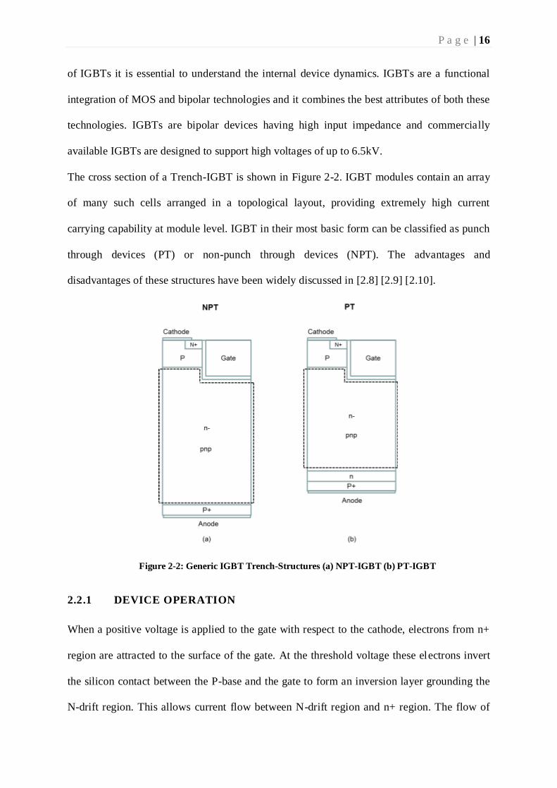
The cross section of a Trench-IGBT is shown in Figure 2-2. IGBT modules contain an array
of many such cells arranged in a topological layout, providing extremely high current
carrying capability at module level. IGBT in their most basic form can be classified as punch
through devices (PT) or non-punch through devices (NPT). The advantages and
disadvantages of these structures have been widely discussed in [2.8] [2.9] [2.10].
Figure 2-2: Generic IGBT Trench-Structures (a) NPT-IGBT (b) PT-IGBT
2.2.1 DEVICE OPERATION
When a positive voltage is applied to the gate with respect to the cathode, electrons from n+
region are attracted to the surface of the gate. At the threshold voltage these electrons invert
the silicon contact between the P-base and the gate to form an inversion layer grounding the
N-drift region. This allows current flow between N-drift region and n+ region. The flow of

P a g e | 17
electrons into the N-drift region lowers the potential of the N-drift region where the P+
Anode
/ N-drift diode becomes forward biased. This allows a high density of minority carriers to be
injected into the N-drift by the P+ Anode. The minority carrier injected into the N- drift
travels vertically upward and some of these holes are repelled by the positively charged
accumulation layer below the gate. These holes then transverse through the P-base and reach
Cathode contact. At high forward voltages a high density of holes builds up in the N-drift.
These holes attract electrons from the cathode contact to maintain charge neutrality which
drastically enhance the conductivity of N-drift. The increased conductivity modulation of the
N-drift allows flow of electrons through this region with very less resistance. Figure 2-3
shows a graphical interpretation of the flow of charge in an IGBT.
To regain blocking state the gate voltage applied to the devices must be removed and the
charges injected into the bulk region must be extracted. Most of this charge is extracted as the
depletion region moves towards the P+ Anode. However, the decay of excess carriers
happens through the process of recombination and no external circuit can be used to speed up
the process. In punch-through devices a lifetime killing technique can be employed to
decrease the turn-off time and losses.
Figure 2-3: Graphical interpretation of the flow of charge in an IGBT during its on-state [2.11]

P a g e | 18
2.2.2 DRIFT ENGINEERING
The design of the drift region is driven primarily by the ability of the device to support
voltage, when operated in its forward blocking state. During the on-state, the drift region is
flooded with charge which contributes to its on-state voltage. During turn-off, this charge
needs to be extracted from the drift region as otherwise they contribute to increased turn-off
losses of the device. Therefore, enhancing the conductivity modulation of the device can
potentially give rise to an increase in the turn-off losses of the device. In a NPT (Non-punch
through) IGBT, the drift region is uniformly doped and the length of the drift region must be
sufficient to support the electric field. In a PT (punch through) device, the length of the drift
region is reduced by introducing a heavily doped buffer region. The thickness of the buffer
region is adjusted to support the expansion of depletion region avoiding premature
breakdown due to punch through. However, there are many disadvantages to the punch
through structure which are highlighted in [2.12], a brief summary of this is shown below.
The epitaxial growth of PT IGBT more than 100µm thick is difficult and expensive.
As the epitaxial layer is grown on heavily doped regions, it inserts a large
concentration of minority carriers increasing the turn-off time of the device.
Limits high frequency switching due to higher turn-off losses.
The PT IGBT has a negative temperature co-efficient of the forward voltage drop.
This essentially means the devices are difficult to parallel. Therefore requires further
optimisation of the buffer region.
These drawbacks led to the development of the field stop structure which uses a transparent
anode (such as that in an NPT IGBT) and buffer region which is less doped in comparison to
the punch-through structure. This combination achieves low on-state voltage during the on-
state and also supports the DC-link voltage in forward blocking mode. The field stop
structure has a positive temperature co-efficient in comparison to a punch-through structure,
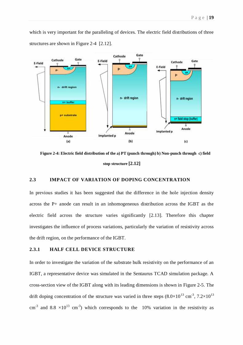
P a g e | 19
which is very important for the paralleling of devices. The electric field distributions of three
structures are shown in Figure 2-4 [2.12].
Figure 2-4: Electric field distribution of the a) PT (punch through) b) Non-punch through c) field
stop structure [2.12]
2.3 IMPACT OF VARIATION OF DOPING CONCENTRATION
In previous studies it has been suggested that the difference in the hole injection density
across the P+ anode can result in an inhomogeneous distribution across the IGBT as the
electric field across the structure varies significantly [2.13]. Therefore this chapter
investigates the influence of process variations, particularly the variation of resistivity across
the drift region, on the performance of the IGBT.
2.3.1 HALF CELL DEVICE STRUCTURE
In order to investigate the variation of the substrate bulk resistivity on the performance of an
IGBT, a representative device was simulated in the Sentaurus TCAD simulation package. A
cross-section view of the IGBT along with its leading dimensions is shown in Figure 2-5. The
drift doping concentration of the structure was varied in three steps (8.0×10¹³
cm-3
, 7.2×10¹³
cm-3
and 8.8 ×10¹³
cm-3
) which corresponds to the 10% variation in the resistivity as

P a g e | 20
discussed in section 2.1. The breakdown voltage of the structure was designed to be 1.2kV,
(by appropriate setting of the thickness of the drift region) and the cell dimensions of the
IGBT are in line with sub-micro device technologies.
Figure 2-5: Cross section view of the IGBT along with its leading dimensions
2.3.1.1 SIMULATION RESULTS
A series of predicted static characteristics for the device with the different drift doping
concentrations considered are summarised in Table 2-2. The inductive switching performance
of the trench IGBT structure for the various drift doping concentrations is shown in Figure
2-7. The test setup used for simulation is shown in Figure 2-6.
Table 2-2: Simulated static characteristics of 1.2kV Trench-IGBT
1. Structure
Drift
Concentration
Oxide
Thickness
Temperature
(°C)
Threshold
voltage
(Volts)
Breakdown
Voltage
(Volts)
Vce(sat)
(Volts)
IGBT
7.2x10¹³
cm-3
0.0979µm 25 5.02 1424 1.61
125 4.06 1684 1.99
8.0 x10¹³
cm-3
0.0979µm 25 5.02 1385 1.61
125 4.05 1654 1.99
8.8 x10¹³
cm-3
0.0979µm 25 4.99 1364 1.61
125 4.07 1630 1.99
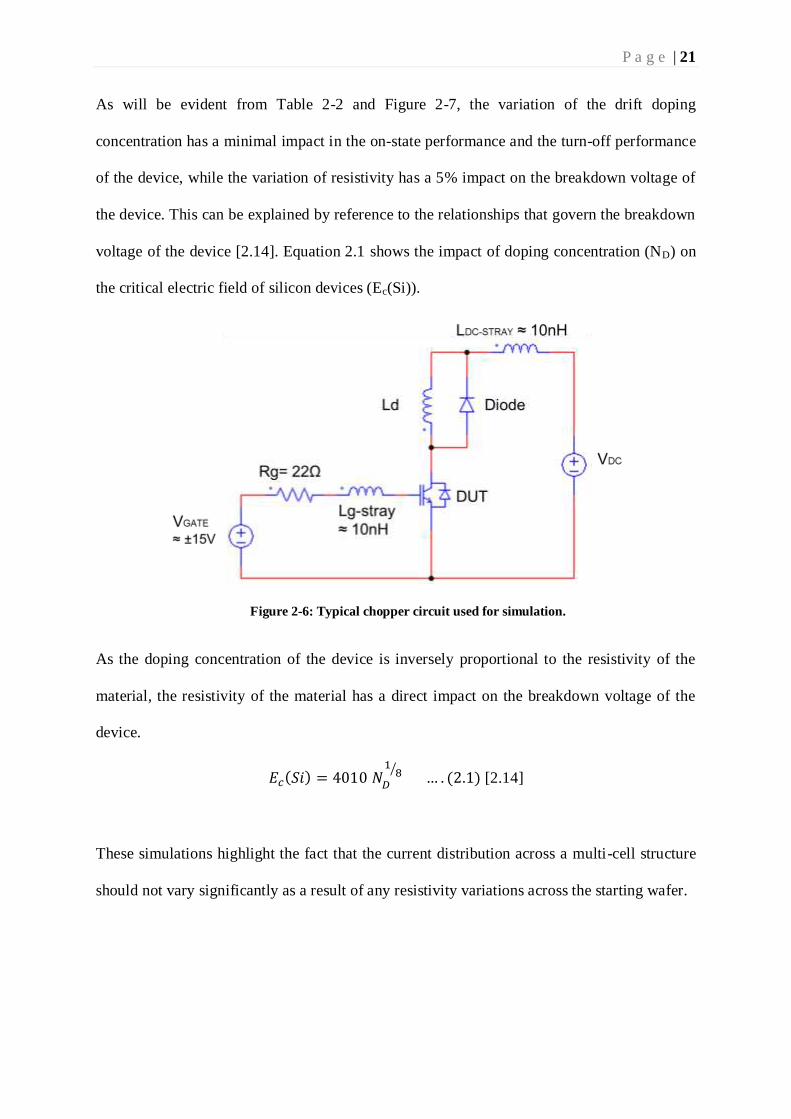
P a g e | 21
As will be evident from Table 2-2 and Figure 2-7, the variation of the drift doping
concentration has a minimal impact in the on-state performance and the turn-off performance
of the device, while the variation of resistivity has a 5% impact on the breakdown voltage of
the device. This can be explained by reference to the relationships that govern the breakdown
voltage of the device [2.14]. Equation 2.1 shows the impact of doping concentration (ND) on
the critical electric field of silicon devices (Ec(Si)).
Figure 2-6: Typical chopper circuit used for simulation.
As the doping concentration of the device is inversely proportional to the resistivity of the
material, the resistivity of the material has a direct impact on the breakdown voltage of the
device.
𝐸𝑐(𝑆𝑖) = 4010 𝑁𝐷
18⁄
… . (2.1) [2.14]
These simulations highlight the fact that the current distribution across a multi-cell structure
should not vary significantly as a result of any resistivity variations across the starting wafer.
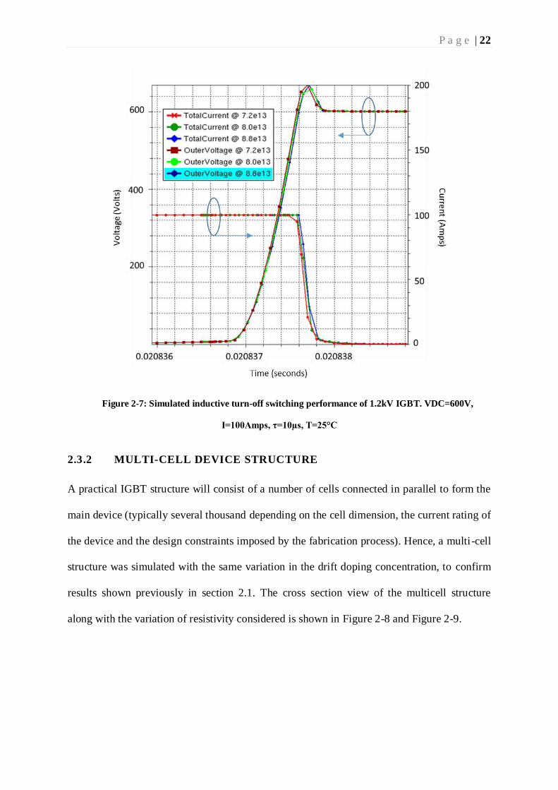
P a g e | 22
Figure 2-7: Simulated inductive turn-off switching performance of 1.2kV IGBT. VDC=600V,
I=100Amps, τ=10µs, T=25°C
2.3.2 MULTI-CELL DEVICE STRUCTURE
A practical IGBT structure will consist of a number of cells connected in parallel to form the
main device (typically several thousand depending on the cell dimension, the current rating of
the device and the design constraints imposed by the fabrication process). Hence, a multi-cell
structure was simulated with the same variation in the drift doping concentration, to confirm
results shown previously in section 2.1. The cross section view of the multicell structure
along with the variation of resistivity considered is shown in Figure 2-8 and Figure 2-9.
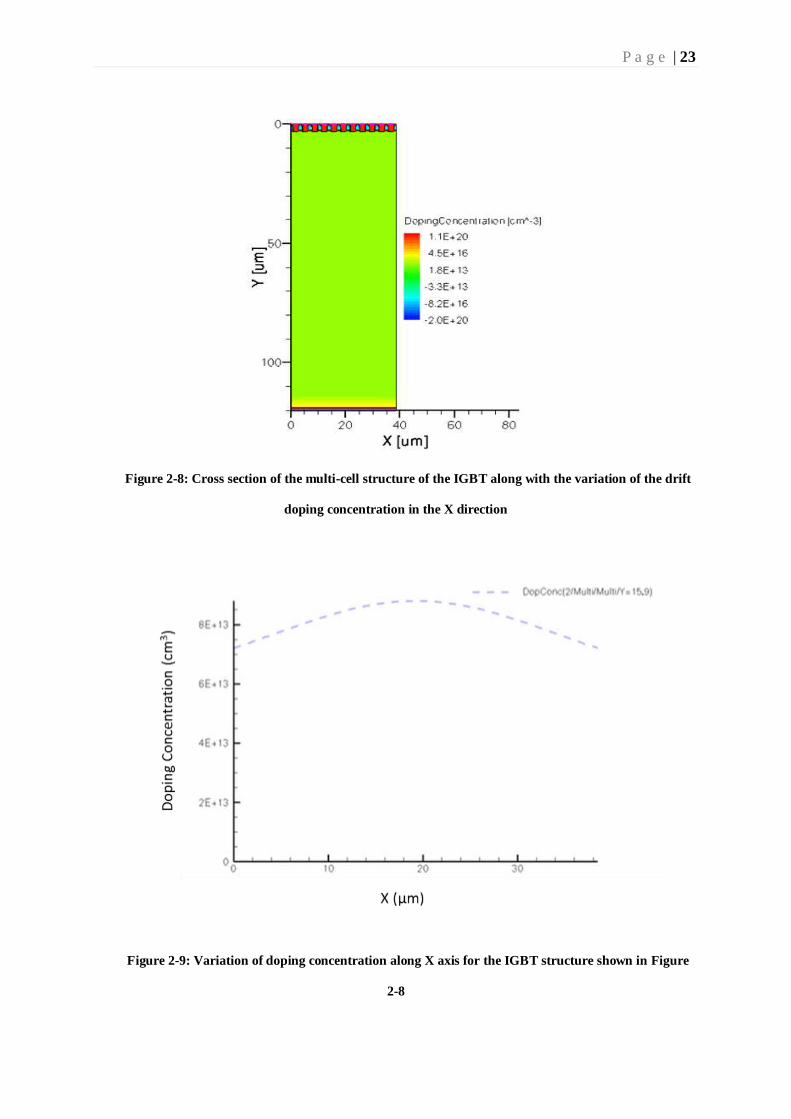
P a g e | 23
Figure 2-8: Cross section of the multi-cell structure of the IGBT along with the variation of the drift
doping concentration in the X direction
Figure 2-9: Variation of doping concentration along X axis for the IGBT structure shown in Figure
2-8
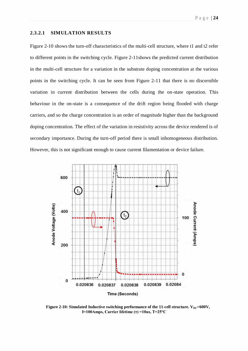
P a g e | 24
2.3.2.1 SIMULATION RESULTS
Figure 2-10 shows the turn-off characteristics of the multi-cell structure, where t1 and t2 refer
to different points in the switching cycle. Figure 2-11shows the predicted current distribution
in the multi-cell structure for a variation in the substrate doping concentration at the various
points in the switching cycle. It can be seen from Figure 2-11 that there is no discernible
variation in current distribution between the cells during the on-state operation. This
behaviour in the on-state is a consequence of the drift region being flooded with charge
carriers, and so the charge concentration is an order of magnitude higher than the background
doping concentration. The effect of the variation in resistivity across the device rendered is of
secondary importance. During the turn-off period there is small inhomogeneous distribution.
However, this is not significant enough to cause current filamentation or device failure.
Figure 2-10: Simulated Inductive switching performance of the 11-cell structure. VDC=600V,
I=100Amps, Carrier lifetime (τ) =10us, T=25°C

P a g e | 25
Figure 2-11: Current distributions across the 11-Cell structure during (a) turn-off condition (b) the
on- state condition
As demonstrated by Figure 2-11 a 10% variation of doping concentration specified above
does not affect device performance to a meaningful extent. The next part of the study is
focused on establishing the maximum variation that can be tolerated without affecting the
device characteristics.
2.3.3 MAXIMUM ACCEPTABLE VARIATION
The unit cell structure shown in Figure 2-5 was considered with homogenous base
concentration in order to establish whether there was any substantial effect on the static
performance of the device. Figure 2-12 shows the effect of variation of resistivity on the
threshold and saturation characteristics of the device with the baseline drift doping
concentration of around 1x10¹⁴
cm-3
identified by the green marker. It can be seen that there
is a minimal variation in both of the properties and therefore the short-circuit performance of
the devices should also not be influenced by the variation of the drift resistivity. Figure 2-13
shows the influence of variation in resistivity (resistivity of the material is inversely
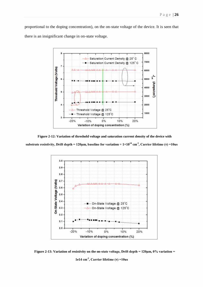
P a g e | 26
proportional to the doping concentration), on the on-state voltage of the device. It is seen that
there is an insignificant change in on-state voltage.
Figure 2-12: Variation of threshold voltage and saturation current density of the device with
substrate resistivity, Drift depth = 120μm, baseline for variation = 1×10¹⁴
cm-3
, Carrier lifetime (τ) =10us
Figure 2-13: Variation of resistivity on the on-state voltage, Drift depth = 120μm, 0% variation =
1e14 cm-3
, Carrier lifetime (τ) =10us
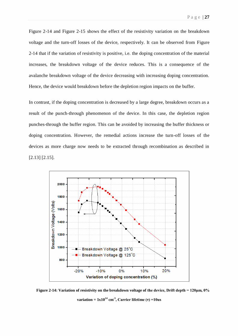
P a g e | 27
Figure 2-14 and Figure 2-15 shows the effect of the resistivity variation on the breakdown
voltage and the turn-off losses of the device, respectively. It can be observed from Figure
2-14 that if the variation of resistivity is positive, i.e. the doping concentration of the material
increases, the breakdown voltage of the device reduces. This is a consequence of the
avalanche breakdown voltage of the device decreasing with increasing doping concentration.
Hence, the device would breakdown before the depletion region impacts on the buffer.
In contrast, if the doping concentration is decreased by a large degree, breakdown occurs as a
result of the punch-through phenomenon of the device. In this case, the depletion region
punches-through the buffer region. This can be avoided by increasing the buffer thickness or
doping concentration. However, the remedial actions increase the turn-off losses of the
devices as more charge now needs to be extracted through recombination as described in
[2.13] [2.15].
Figure 2-14: Variation of resistivity on the breakdown voltage of the device, Drift depth = 120μm, 0%
variation = 1x10¹⁴
cm-3
, Carrier lifetime (τ) =10us

P a g e | 28
Figure 2-15: Variation of resistivity on the turn-off losses on the device, Drift depth = 120μm, 0%
variation=1x10¹⁴
cm-3
, Carrier lifetime (τ) =10us
2.4 CONCLUSION
The results presented in this chapter demonstrate that a variation in substrate resistivity (at
least within reasonable bounds expected within a controlled production environment) will not
impact the device performance to any meaningful degree in terms of on-state voltage and
switching performance. However a significant variation in substrate resistivity can lead to
changes in the device properties across the cell, such as the breakdown voltage and turn-off
losses as presented above.
This means that when devices are paralleled to form a power module, the mismatch in device
properties can lead to premature failure of the power module. To avoid such behaviour, it
would be prudent to conclude that the variation of resistivity should be as low as possible.
Device manufacturers currently consider a substrate resistivity variation of less than 5%
across the wafer. The results presented above justify this choice such that any variation in

P a g e | 29
device characteristics does impact the operation of the power module and the converter
thereof.
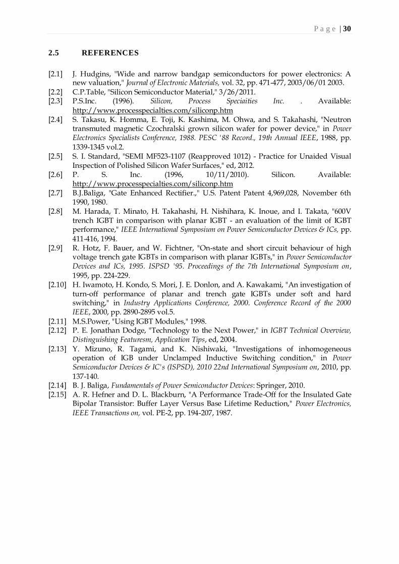
P a g e | 30
2.5 REFERENCES
[2.1] J. Hudgins, "Wide and narrow bandgap semiconductors for power electronics: A new valuation," Journal of Electronic Materials, vol. 32, pp. 471-477, 2003/06/01 2003.
[2.2] C.P.Table, "Silicon Semiconductor Material," 3/26/2011. [2.3] P.S.Inc. (1996). Silicon, Process Speciaities Inc. . Available:
http://www.processpecialties.com/siliconp.htm [2.4] S. Takasu, K. Homma, E. Toji, K. Kashima, M. Ohwa, and S. Takahashi, "Neutron
transmuted magnetic Czochralski grown silicon wafer for power device," in Power Electronics Specialists Conference, 1988. PESC '88 Record., 19th Annual IEEE, 1988, pp. 1339-1345 vol.2.
[2.5] S. I. Standard, "SEMI MF523-1107 (Reapproved 1012) - Practice for Unaided Visual Inspection of Polished Silicon Wafer Surfaces," ed, 2012.
[2.6] P. S. Inc. (1996, 10/11/2010). Silicon. Available: http://www.processpecialties.com/siliconp.htm
[2.7] B.J.Baliga, "Gate Enhanced Rectifier.," U.S. Patent Patent 4,969,028, November 6th 1990, 1980.
[2.8] M. Harada, T. Minato, H. Takahashi, H. Nishihara, K. Inoue, and I. Takata, "600V trench IGBT in comparison with planar IGBT - an evaluation of the limit of IGBT performance," IEEE International Symposium on Power Semiconductor Devices & ICs, pp. 411-416, 1994.
[2.9] R. Hotz, F. Bauer, and W. Fichtner, "On-state and short circuit behaviour of high voltage trench gate IGBTs in comparison with planar IGBTs," in Power Semiconductor Devices and ICs, 1995. ISPSD '95. Proceedings of the 7th International Symposium on, 1995, pp. 224-229.
[2.10] H. Iwamoto, H. Kondo, S. Mori, J. E. Donlon, and A. Kawakami, "An investigation of turn-off performance of planar and trench gate IGBTs under soft and hard switching," in Industry Applications Conference, 2000. Conference Record of the 2000 IEEE, 2000, pp. 2890-2895 vol.5.
[2.11] M.S.Power, "Using IGBT Modules," 1998. [2.12] P. E. Jonathan Dodge, "Technology to the Next Power," in IGBT Technical Overview,
Distinguishing Featuresm, Application Tips, ed, 2004. [2.13] Y. Mizuno, R. Tagami, and K. Nishiwaki, "Investigations of inhomogeneous
operation of IGB under Unclamped Inductive Switching condition," in Power Semiconductor Devices & IC's (ISPSD), 2010 22nd International Symposium on, 2010, pp. 137-140.
[2.14] B. J. Baliga, Fundamentals of Power Semiconductor Devices: Springer, 2010. [2.15] A. R. Hefner and D. L. Blackburn, "A Performance Trade-Off for the Insulated Gate
Bipolar Transistor: Buffer Layer Versus Base Lifetime Reduction," Power Electronics,
IEEE Transactions on, vol. PE-2, pp. 194-207, 1987.
P a g e | 31
CHAPTER THREE
Chapter 3
EVALUATION OF 3.3kV PLANAR CIGBT IN NON-PUNCH THROUGH
TECHNOLOGY
3.1 INTRODUCTION
MOS controlled bipolar devices such as IGBTs are commercially available for a blocking
voltage range of up to 6.5kV [3.1]. Beyond 3.3kV, IGBTs begin to compete with Gate turn-
off thyristor (GTOs) and it becomes increasingly important to optimise their performance,
both in terms of their on-state and switching losses.
In this chapter, a 3.3kV rated CIGBT (Clustered Insulated Gate Bipolar Transistor) with
planar gates in Non Punch Through technology (NPT) with Rapid Thermal Annealing (RTA)
anode, is evaluated. The benefits of using an RTA anode structure as compared to a diffused
anode structure in an NPT technology are discussed. Previously it has been shown [3.2], that
for identical turn-off losses, the on-state voltage of a 3.3kV NPT-CIGBT was 2.3Volts which
is less than 0.7 Volts as compared to that of a commercially available Field Stop(FS) IGBT.
In this chapter, the optimisation of the switching performance of the device is addressed by
using a RTA anode structure. This approach maintains a similar on-state voltage as that of a
diffused anode structure. This chapter also evaluates the various structural parameters of the
MOS clusters located within the P-WELL region and the variation of the N-WELL implant
dose.
3.2 TRANSPARENT ANODE DESIGN
The turn-off and on-state conduction losses of Silicon based MOS controlled bipolar
structures can be optimised by using various methods. The traditional approach to reducing
the switching losses in the device is based on reducing the lifetime of the carriers in the drift
region to accelerate the recombination of the stored charge. This method has been widely

P a g e | 32
adopted by industry. However, this increases the on-state voltage of the device considerably,
as less stored charge is now available for forward conduction. The second method used by
semiconductor manufactures to reduce switching losses is to employ a thinner and lightly
doped anode/collector region. This method is commonly referred to as the Transparent Anode
Structure or a Transparent Emitter Structure since the anode or the collector region behaves
as an emitter, to inject minority carriers into the drift region. To aid this discussion, a
schematic cross section of a representative CIGBT structure along with its equivalent circuit
is shown in Figure 3-1.
Figure 3-1: A schematic of the NPT-CIGBT cell along with its equivalent circuit.
In the on-state, the P-ANODE region and N-BASE junction is forward biased and the
electrons flowing from the cathode side are injected into the P-ANODE region where they
recombine. In a transparent anode structure, the electrons injected into the P-ANODE region
diffuse to the collector contact without significant recombination within the P-ANODE
region. Since the thickness of this region is set to be much shorter than the diffusion length
the electron concentration at the contact can be assumed to be zero as the recombination rate
would be significantly higher due to an ohmic contact. The use of such a transparent anode

P a g e | 33
does not reduce the on-state voltage of the device considerably as a high-level lifetime is
maintained in the drift region. However, the turn-off losses of the device are reduced
considerably as there is less stored charge in the drift region during the turn-off phase.
3.3 DEVICE STRUCTURE AND OPERATION
CIGBT is a three terminal MOS controlled thyristor which has been experimentally
demonstrated at 1200V 1700V, 3300V ratings [3.2] [3.3] [3.4]. A schematic cross section of
a typical CIGBT structure was shown previously in Figure 3-1 The CIGBT consists of a
number of closely packed MOS cells enclosed within floating N-WELL and P-WELL layers
to form clusters. Within each cluster, the P-bases can be arranged as squares, stripes or
circles. A number of these clusters form the overall device active area. The influence of the
number of clusters on the on-state and turn-off performance of the device is discussed in
[3.5].
The operating mechanism of a CIGBT has been discussed in literature many times [3.6] [3.7]
and has been summarised here for clarity. The MOS gate which extends over the P-WELL
region acts as a turn-on gate and the rest of the MOS gates act as control gates. All the gates
are electrically connected together to form a three terminal structure. When a positive voltage
is applied to the gate with respect to the cathode terminal an inversion layer is created
underlying the gate region. The threshold voltage of the structure is adjusted based on the
concentration of the P-base, and is designed similar to the IGBT cells for comparison. The
creation of the inversion layer grounds the N-WELL and N-BASE region via the inversion
and accumulation regions. The P-WELL region is floating under this condition and is
capacitively coupled to anode. Therefore, the potential of the P-WELL region increases with
the anode potential. When the potential drop across the P-WELL / N-WELL junction rises
above the built in potential, the thyristor formed by the P-ANODE/N-BASE/ P-WELL/ N-

P a g e | 34
WELL regions is triggered without a snapback. In the conduction mode of operation, the P-
BASE/N-WELL junction is reverse biased and as the anode voltage increases, the depletion
region of this junction extends towards the N-WELL region resulting in punch through at a
predefined voltage. Once punch though has occurred the potential of this region does not
increase anymore and any further increase in the anode potential is dropped across the P-
WELL and N-BASE regions. This prevents high electric field from reaching the cathode
region. The anode voltage at which the punch through occurs is known the Self-clamping
voltage (Vscl). Self-clamping also helps to limit the saturation current density (Jsat) [3.7]
and realise fast switching. CIGBT therefore provides a complete MOS gate control over
thyristor conduction mode.
3.4 EXPERIMENTAL RESULTS
For this study, research dies rated at 50A and 6A with dimensions of 12.5x12.5 mm2 and 7x7
mm2 respectively were fabricated in 4”, 300 Ω cm, 500µm thick Silicon wafers as shown in
Figure 3-2. The active areas for the 6A and 50A devices are 10.8mm2 and 94.2mm
2
respectively.
Figure 3-2: A fabricated wafer showing devices rated 50A and 6A. The layout contains several
CIGBT and IGBT designs for comparison
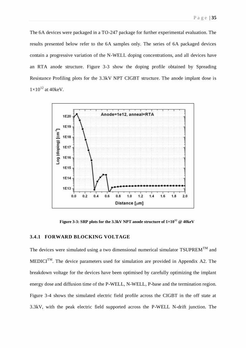
P a g e | 35
The 6A devices were packaged in a TO-247 package for further experimental evaluation. The
results presented below refer to the 6A samples only. The series of 6A packaged devices
contain a progressive variation of the N-WELL doping concentrations, and all devices have
an RTA anode structure. Figure 3-3 show the doping profile obtained by Spreading
Resistance Profiling plots for the 3.3kV NPT CIGBT structure. The anode implant dose is
1×10¹²
at 40keV.
Figure 3-3: SRP plots for the 3.3kV NPT anode structure of 1×10¹²
@ 40keV
3.4.1 FORWARD BLOCKING VOLTAGE
The devices were simulated using a two dimensional numerical simulator TSUPREMTM
and
MEDICITM
. The device parameters used for simulation are provided in Appendix A2. The
breakdown voltage for the devices have been optimised by carefully optimizing the implant
energy dose and diffusion time of the P-WELL, N-WELL, P-base and the termination region.
Figure 3-4 shows the simulated electric field profile across the CIGBT in the off state at
3.3kV, with the peak electric field supported across the P-WELL N-drift junction. The
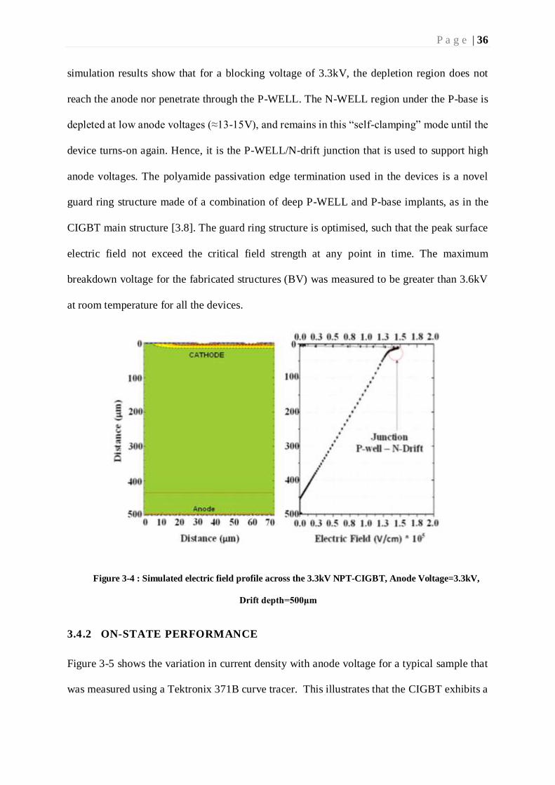
P a g e | 36
simulation results show that for a blocking voltage of 3.3kV, the depletion region does not
reach the anode nor penetrate through the P-WELL. The N-WELL region under the P-base is
depleted at low anode voltages (≈13-15V), and remains in this “self-clamping” mode until the
device turns-on again. Hence, it is the P-WELL/N-drift junction that is used to support high
anode voltages. The polyamide passivation edge termination used in the devices is a novel
guard ring structure made of a combination of deep P-WELL and P-base implants, as in the
CIGBT main structure [3.8]. The guard ring structure is optimised, such that the peak surface
electric field not exceed the critical field strength at any point in time. The maximum
breakdown voltage for the fabricated structures (BV) was measured to be greater than 3.6kV
at room temperature for all the devices.
Figure 3-4 : Simulated electric field profile across the 3.3kV NPT-CIGBT, Anode Voltage=3.3kV,
Drift depth=500μm
3.4.2 ON-STATE PERFORMANCE
Figure 3-5 shows the variation in current density with anode voltage for a typical sample that
was measured using a Tektronix 371B curve tracer. This illustrates that the CIGBT exhibits a

P a g e | 37
snap-back free turn-on and its Vce(sat) has a positive temperature coefficient. The
temperature co-efficient of on-state voltage at 125°C is some 1.39 times the value at 25°C.
Figure 3-5 further shows that the saturation current density of the CIGBT can be controlled to
4 times its rated current at 125°C. This is necessary to enhance the short circuit performance
of the device.
Figure 3-5: Typical experimental CIGBT on-state I (V) at 25°C and 125°C, Vg=+15V
Figure 3-6 shows the variation in current saturation at high gate voltages, measured using
Tektronix 371B curve tracer. The enhanced current saturation capability of the CIGBT as
compared to any other known MOS controlled thyristor, is due to its ‘self-clamping’ feature
which limits the potential within the MOS clusters and prevents premature breakdown of the
N-channel MOSFETs [3.6] [3.9]. The lower Vce(sat) of a CIGBT is because its on-state
conduction is via a controlled thyristor action rather than the pnp transistor in the IGBT [3.6].
The thyristor action allows more charge to be injected into the drift region, in turn allowing a
higher conductivity modulation within the drift region. Figure 3-7 shows that the thyristor
conduction in CIGBT results in excellent conductivity modulation within the cathode area of

P a g e | 38
the device, which is more than twice that of an equivalent rated IGBT. Apart from exhibiting
a low Vce(sat), another very important feature of CIGBTs is that the current saturation level
can be controlled to only few multiples of the rated current.
Figure 3-6: Experimentally measured CIGBT current saturation characteristics Vth = 5.5V, Tj=
25°C
Figure 3-7: Simulated carrier density profile within the CIGBT compared with IGBT at JA = 50Acm-2

P a g e | 39
3.4.2.1 INFLUENCE OF CATHODE CELL GEOMETRY
It has been previously shown in [3.4] that the P-base spacing in the NPT-CIGBT has a minor
influence on its Vce(sat) because its N-WELL doping is in the region of 1016
cm-3
[3.4]. It has
also been shown in [3.2], that the circular geometric cell design leads to be slightly lower
Vce(sat) than that of a rectangular cathode cell geometry. The lower Vce(sat) and higher Jsat
for the circular cathode cell design can be explained in terms of area (A), and perimeter (P)
(of the MOS channels). Figure 3-8 shows the layout of the circular and square designs. From
equation 3.1 and 3.2 it can be said that the square cell design is 1.27 times larger as compared
to the circular design.
𝐴𝑠𝑞𝑢𝑎𝑟𝑒
𝐴𝐶𝑖𝑟𝑐𝑙𝑒=
4 𝑟2
𝜋𝑟2 = 1.27 …. (3.1)
𝑃𝑠𝑞𝑢𝑎𝑟𝑒
𝑃𝐶𝑖𝑟𝑐𝑙𝑒=
8𝑟
2𝜋r= 1.27 …. (3.2)
Figure 3-8: Schematic of the cathode cells showing the N-WELL and P-base circular and square
designs in CIGBT
The smaller area of the circular design means that less N-WELL area is counter doped by the
P-base, and its slightly shorter channel length ensures that there is more electron current than
is the case with the square design. This results in an improved conductivity modulation, but
at the expense of a higher Jsat.

P a g e | 40
3.4.2.2 INFLUENCE OF N-WELL IMPLANT DOSE
The N-WELL implant dose influences both, the on-state voltage and saturation characteristics
of the devices as shown by the experimental measurement on the 6 A samples in Figure 3-9.
These experimental results show that an improvement in the on-state performance can be
achieved by using a higher N-WELL implant dose, as better conductivity modulation can be
achieved by increasing the NPN (N-WELL/P-WELL/N-drift) gain of the thyristor. However,
Increasing the N-WELL dose also increases the saturation current density of the device,
which in turn will impact its short circuit capability and reduce its safe operating area (SOA).
Figure 3-9: Experimental results on the influence of N-WELL dose (Nw1 (6.9e13) > Nw2 (6.7e13) > Nw3
(6.5e13)) on the on-state voltage Vce(sat) and saturation current density of CIGBT at 25°C
This behaviour arises because higher N-WELL dose increases the quantity of charge to be
depleted, thereby increasing the self-clamping voltage. In addition, increasing the N-WELL
concentration counter-dopes the P-base which can result in a reduction of the Vth (threshold
voltage) of the device. Hence, careful consideration must be given to the level of N-WELL

P a g e | 41
implant dose. The amount of charge in the N-WELL is related to the self-clamping voltage
and is shown in equation 3.3 [3.10].
𝑉𝑠𝑐𝑙 =(𝑊𝑛−𝑤𝑒𝑙𝑙− 𝐿𝑃)2𝑞𝑁𝑏
2𝜀𝜀0 … (3.3)
Where Vscl is the punch through voltage, Nb is the N-WELL doping concentration, WN-WELL
is the depth of N-WELL, Lp is diffusion length, q is the electronic charge, εo= permittivity of
free space and ε = permittivity of silicon, q= electron elementary charge.
Figure 3-10: Simulated carrier density comparison of the 3.3kV CIGBT structure with variation of
the N-WELL implant dose (Nw1 (6.9e13) > Nw2 (6.7e13) > Nw3 (6.5e13))
Figure 3-10 shows the simulated influence of the N-WELL implant dose on the carrier
density profile within CIGBT. The results clearly show that the thyristor conduction in
CIGBT can be improved as the N-WELL concentration is improved. Nw1 exhibits an order
of magnitude improvement in carrier concentration compared to Nw3. Figure 3-11 shows the
simulated influence of the N-WELL doping on the self-clamping voltage of the device. As
the N-WELL dose is increased, more voltage is required to deplete the N-WELL regions
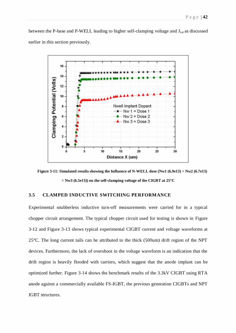
P a g e | 42
between the P-base and P-WELL leading to higher self-clamping voltage and Jsat as discussed
earlier in this section previously.
Figure 3-11: Simulated results showing the Influence of N-WELL dose (Nw1 (6.9e13) > Nw2 (6.7e13)
> Nw3 (6.5e13)) on the self-clamping voltage of the CIGBT at 25°C
3.5 CLAMPED INDUCTIVE SWITCHING PERFORMANCE
Experimental snubberless inductive turn-off measurements were carried for in a typical
chopper circuit arrangement. The typical chopper circuit used for testing is shown in Figure
3-12 and Figure 3-13 shows typical experimental CIGBT current and voltage waveforms at
25°C. The long current tails can be attributed to the thick (500um) drift region of the NPT
devices. Furthermore, the lack of overshoot in the voltage waveform is an indication that the
drift region is heavily flooded with carriers, which suggest that the anode implant can be
optimized further. Figure 3-14 shows the benchmark results of the 3.3kV CIGBT using RTA
anode against a commercially available FS-IGBT, the previous generation CIGBTs and NPT
IGBT structures.
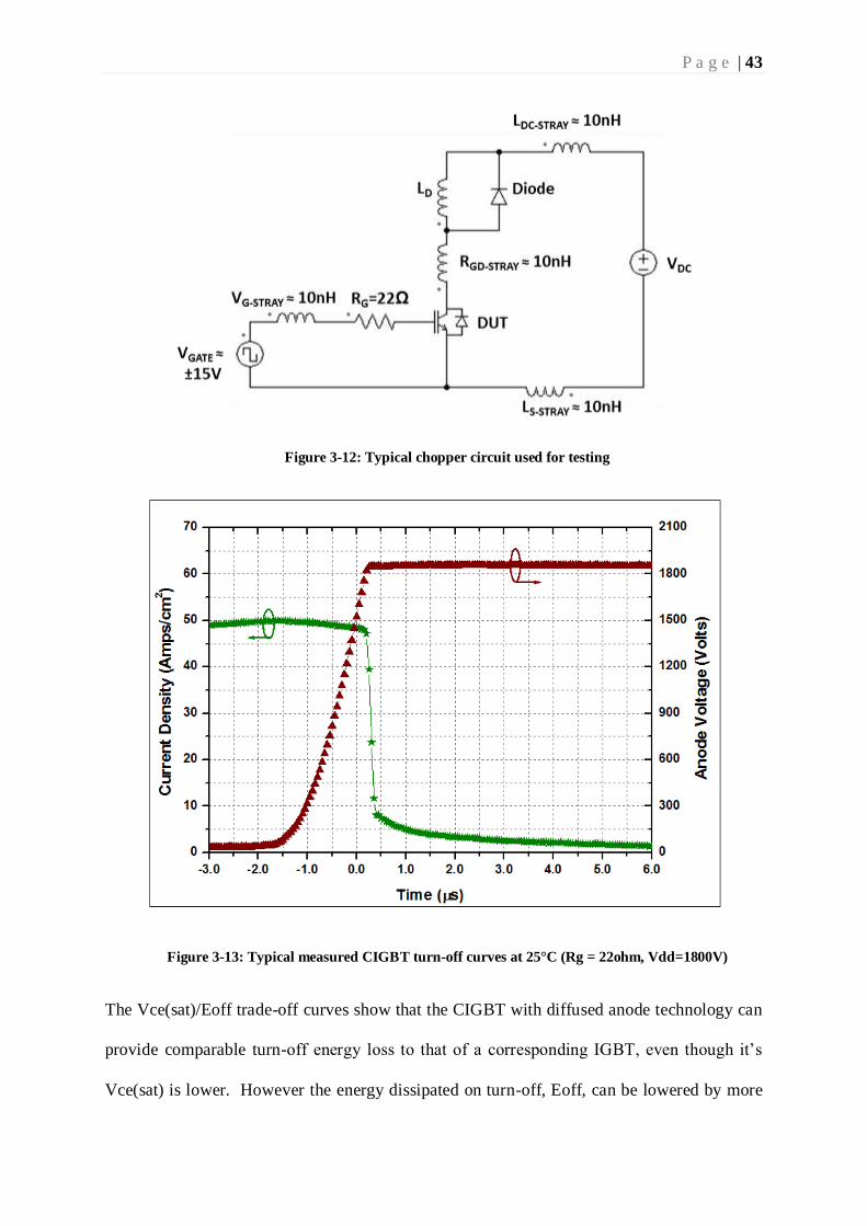
P a g e | 43
Figure 3-12: Typical chopper circuit used for testing
Figure 3-13: Typical measured CIGBT turn-off curves at 25°C (Rg = 22ohm, Vdd=1800V)
The Vce(sat)/Eoff trade-off curves show that the CIGBT with diffused anode technology can
provide comparable turn-off energy loss to that of a corresponding IGBT, even though it’s
Vce(sat) is lower. However the energy dissipated on turn-off, Eoff, can be lowered by more

P a g e | 44
than 50% with RTA anode compared to diffused anode technology. Such levels are better
than commercially available Field Stop-IGBT structures. The reduction in turn-off losses can
be attributed to the reduced current tail due to a more transparent anode structure as discussed
in section 3.2 of this chapter. The device provided by Company-A uses Field Stop technology
and is thinner than the NPT devices. Therefore the use of Field stop technology in the RTA
anode structure can boost the performance even more.
Figure 3-14: Comparison of experimental NPT-CIGBT and IGBT trade-off curves at 25°C.
A1>A2>A3>A4, Rg = 22Ω, Vdd = 1800V
The low turn-off loss in a CIGBT design can be explained as follows:-
The ‘self-clamping’ phenomenon which occurs when the anode potential is <20V is
maintained throughout the turn-off process, and only disappears when the device turns on
again. Hence, during turn-off, the holes which are collected within the P-WELL region flow
to the cathode contact at the saturation velocity through the high electric field depleted N-
WELL regions as shown in Figure 3-15. This mechanism is very efficient, and results in fast

P a g e | 45
turn-off speed and low turn-off loss (Eoff). Figure 3-16 show that the CIGBT with RTA
anode can readily turn-off more than 3 times the rated current at 25°C. This indicates that the
CIGBT can be used in rugged applications.
Figure 3-15: Simulated CIGBT current flow during turn-off showing holes flowing through the
depleted N-WELL regions
Figure 3-16: Typically measured CIGBT turn-off at 25°C (Rg = 100ohm, Vdd=1650V) for Vg=+15V

P a g e | 46
3.6 UNCLAMPED INDUCTIVE SWITCHING PERFORMANCE
The unclamped inductive switching (UIS) conditions are high stress switching conditions
where the devices are subjected to high current and high voltage simultaneously, when the
freewheeling diode in parallel with the load fails. The experimental test circuit for the UIS
operating mode is shown in Figure 3-17. The load inductor is unclamped as there is no
freewheeling diode to discharge the inductor energy when the device turns off.
Figure 3-18 shows the general waveforms that would be expected when a device is operated
under UIS. The pulse on the gate of the device is applied over the interval t1 to t2. During
this interval, the current will ramp up through the device and the inductor, reaching a peak
value Ip. At time t2, the device is turned off by reducing the gate voltage to 0V s. At this time,
the energy stored in the inductor must be dissipated. However, the absence of the
freewheeling diode means that the energy stored will be dissipated thought the device. This
forces the device into its avalanche breakdown mode until the inductor is effectively fully
discharged.
Figure 3-17: Test Circuit used to study the CIGBT behaviour under UIS
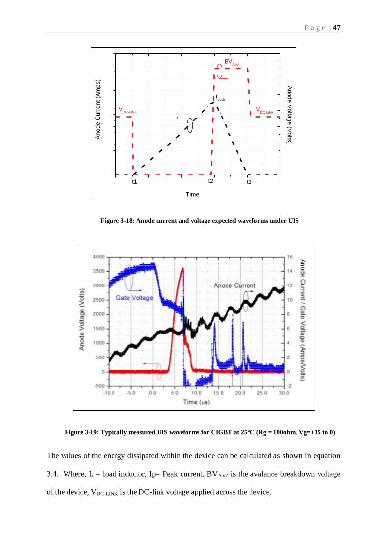
P a g e | 47
Figure 3-18: Anode current and voltage expected waveforms under UIS
Figure 3-19: Typically measured UIS waveforms for CIGBT at 25°C (Rg = 100ohm, Vg=+15 to 0)
The values of the energy dissipated within the device can be calculated as shown in equation
3.4. Where, L = load inductor, Ip= Peak current, BVAVA is the avalance breakdown voltage
of the device, VDC-LINK is the DC-link voltage applied across the device.
Ipeak
VDC-LINK
VDC-LINK
BVAVA
t3t2t1
An
od
e V
olta
ge
(Vo
lts)A
no
de
Cu
rre
nt (A
mp
s)
Time

P a g e | 48
𝐸𝐷 =1
2LIp
2 ∗ (BVAVA
BVAVA−VDC−LINK) …. (3.4)
Figure 3-19 shows that the CIGBT under test is unable to withstand the UIS condition at full
rated current. It can be seen that the anode current continues to ramp up as the device enters
into avalanche mode. Various IGBT failure methods been reported in literature [3.11].
However, the main reason for the CIGBT failure under UIS is due to the variation of the
poly-sheet resistance. This essentially means that the cells at the periphery of the device are
not able to turn-off as quickly as those closer to the gate. This causes inhomogeneous current
distribution within the device leading to device failure under UIS condition. Figure 3-20
shows the measured UIS waveforms when the anode voltage and peak current flowing
through the device is reduced. Under this condition, the CIGBT is able to withstand the stress
condition for a short period of time as the device enters into avalanche mode, allowing the
cells in the periphery to turn-off quickly.
Figure 3-20: Measured UIS waveforms for CIGBT at 25°C (Vanode=400V, Rg = 100ohm, Vg=+15 to
0)
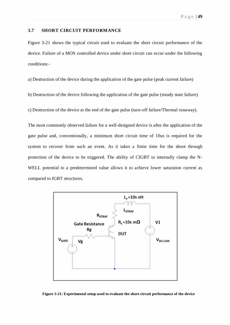
P a g e | 49
3.7 SHORT CIRCUIT PERFORMANCE
Figure 3-21 shows the typical circuit used to evaluate the short circuit performance of the
device. Failure of a MOS controlled device under short circuit can occur under the following
conditions:-
a) Destruction of the device during the application of the gate pulse (peak current failure)
b) Destruction of the device following the application of the gate pulse (steady state failure)
c) Destruction of the device at the end of the gate pulse (turn-off failure/Thermal runaway).
The most commonly observed failure for a well-designed device is after the application of the
gate pulse and, conventionally, a minimum short circuit time of 10us is required for the
system to recover from such an event. As it takes a finite time for the shoot through
protection of the device to be triggered. The ability of CIGBT to internally clamp the N-
WELL potential to a predetermined value allows it to achieve lower saturation current as
compared to IGBT structures.
Figure 3-21: Experimental setup used to evaluate the short-circuit performance of the device
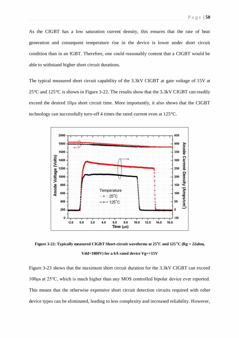
P a g e | 50
As the CIGBT has a low saturation current density, this ensures that the rate of heat
generation and consequent temperature rise in the device is lower under short circuit
condition than in an IGBT. Therefore, one could reasonably content that a CIGBT would be
able to withstand higher short circuit durations.
The typical measured short circuit capability of the 3.3kV CIGBT at gate voltage of 15V at
25°C and 125°C is shown in Figure 3-22. The results show that the 3.3kV CIGBT can readily
exceed the desired 10µs short circuit time. More importantly, it also shows that the CIGBT
technology can successfully turn-off 4 times the rated current even at 125°C.
Figure 3-22: Typically measured CIGBT Short-circuit waveforms at 25oC and 125
oC (Rg = 22ohm,
Vdd=1800V) for a 6A rated device Vg=+15V
Figure 3-23 shows that the maximum short circuit duration for the 3.3kV CIGBT can exceed
100μs at 25°C, which is much higher than any MOS controlled bipolar device ever reported.
This means that the otherwise expensive short circuit detection circuits required with other
device types can be eliminated, leading to less complexity and increased reliability. However,

P a g e | 51
measured results also show that the anode voltage drops with time as the DC-link capacitors
in the system are not able to maintain the voltage during the entire event. The maximum
power dissipated in one cycle is calculated to be 3.36 Watts. Therefore, if the anode voltage
is held at a constant value, the simulated short-circuit period for similar power dissipation is
calculated to be over 80μs and is verified via simulations.
Figure 3-23: Maximum measured CIGBT Short-circuit waveforms at 25oC (Rg = 22ohm,
Vdd=1800V) Vg=+15V
3.7.1 INFLUENCE OF GATE RESISTANCE
Figure 3-24 shows the influence of the gate resistance on the short circuit performance of the
device more specifically that as the gate resistance is reduced, the current overshoot during
the turn-on phase of the device is eliminated for all practical purposes. The overshoot
appearing during the turn-on phase of the device when the gate voltage exceeds the threshold
voltage is a consequence of the accumulation layer created underneath the planar gates,

P a g e | 52
which attracts holes. For a higher value of gate resistance, this causes a feedback effect into
the gate leading to gate voltage amplification which in turn causes the anode current to rise.
Figure 3-24: Typically measured CIGBT Short-circuit waveforms with variation of gate resistance at
25oC (Vdd=1800V)
3.8 CONCLUSION
In this chapter the work done towards the 3.3kV rated CIGBT is presented. The device
fabrication, functionality and the experimental and simulation results are discussed in detail.
The experimental and simulation results presented in this chapter clearly show how the
optimisations of the CATHODE GEOMETRY, the N-WELL and ANODE doping
concentrations have been performed. The experimental results also demonstrate that the
3.3kV rated CIGBT has many aspects of improved performance compared to an equivalent
rated 3.3kV IGBT not only in terms of Vce(sat)/turn-off loss trade-off but also in terms of its
short circuits performance. In addition, it has been shown that the use of RTA anode
technology reduces the turn-off losses of the device by more 50% compared to diffused

P a g e | 53
anode technology. The experimental short-circuit evaluation of the device shows that the
CIGBT can withstand a short circuit time of more than 10μs even at 125°C and has a
maximum short circuit withstand capability of more than 100μs, a value which is much
higher that any MOS controlled bipolar device even reported.
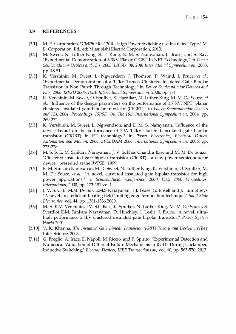
P a g e | 54
3.9 REFERENCES
[3.1] M. E. Corporation, "CM750HG-130R - High Power Switching use Insulated Type," M. E. Corporation, Ed., ed: Mitsubishi Electric Corporation, 2013.
[3.2] M. Sweet, N. Luther-King, S. T. Kong, E. M. S. Narayanan, J. Bruce, and S. Ray, "Experimental Demonstration of 3.3kV Planar CIGBT In NPT Technology," in Power Semiconductor Devices and IC's, 2008. ISPSD '08. 20th International Symposium on, 2008, pp. 48-51.
[3.3] K. Vershinin, M. Sweet, L. Ngwendson, J. Thomson, P. Waind, J. Bruce, et al., "Experimental Demonstration of a 1.2kV Trench Clustered Insulated Gate Bipolar Transistor in Non Punch Through Technology," in Power Semiconductor Devices and IC's, 2006. ISPSD 2006. IEEE International Symposium on, 2006, pp. 1-4.
[3.4] K. Vershinin, M. Sweet, O. Spulber, S. Hardikar, N. Luther-King, M. M. De Souza, et al., "Influence of the design parameters on the performance of 1.7 kV, NPT, planar clustered insulated gate bipolar transistor (CIGBT)," in Power Semiconductor Devices and ICs, 2004. Proceedings. ISPSD '04. The 16th International Symposium on, 2004, pp. 269-272.
[3.5] K. Vershinin, M. Sweet, L. Ngwendson, and E. M. S. Narayanan, "Influence of the device layout on the performance of 20A 1.2kV clustered insulated gate bipolar transistor (CIGBT) in PT technology," in Power Electronics, Electrical Drives, Automation and Motion, 2006. SPEEDAM 2006. International Symposium on, 2006, pp. 275-278.
[3.6] M. S. S. E. M. Sankara Narayanan, J. V. Subhas Chandra Base and M. M. De Souza, "Clustered insulated gate bipolar transistor (CIGBT) - a new power semiconductor device," presented at the IWPSD, 1999.
[3.7] E. M. Sankara Narayanan, M. R. Sweet, N. Luther-King, K. Vershinin, O. Spulber, M. M. De Souza, et al., "A novel, clustered insulated gate bipolar transistor for high power applications," in Semiconductor Conference, 2000. CAS 2000 Proceedings. International, 2000, pp. 173-181 vol.1.
[3.8] J. V. S. C. B. M.M. De So-, E.M.S Narayanan, T.J. Pease, G. Ensell and J. Humphreys "A novel area efficient floating field limiting edge termination technique," Solid State Electronics, vol. 44, pp. 1381-1386 2000.
[3.9] M. S. K.V. Vershinin, J.V. S.C Base, 0. Spulber, N. Luther-King, M. M. De Souza, S. Sverdlof E.M. Sankara Narayanan, D. Hinchley, I. Leslie, J. Bruce, "A novel. ultra-high performance 2.4kV clustered insulated gate bipolar transistor," Power System World 2001.
[3.10] V. K. Khanna, The Insulated Gate Biploar Transistor (IGBT) Theory and Design.: Wiley Inter-Science, 2003.
[3.11] G. Breglio, A. Irace, E. Napoli, M. Riccio, and P. Spirito, "Experimental Detection and Numerical Validation of Different Failure Mechanisms in IGBTs During Unclamped Inductive Switching," Electron Devices, IEEE Transactions on, vol. 60, pp. 563-570, 2013.

P a g e | 55
CHAPTER FOUR
Chapter 4
SEGMENTED P-BASE CLUSTERED INSULATED GATE BIPOLAR
JUNCTION TRANSISTOR
4.1. INTRODUCTION
This chapter evaluates the merits of incorporating a segmented P-base into a trench CIGBT
structure to further improve the carrier concentration at the cathode side without degrading
the short circuit capability and Eoff-Vce(sat) trade-off. The influence of the structural
parameters of the segmented P-base device is investigated in detail using the two-dimensional
numerical device simulator, MEDICITM
. In addition, the functionality of the PMOS (turn-off
gates) gate is also reviewed and discussed in detail.
4.2. ELECTRON INJECTION EFFICIENCY
This section highlights the importance of carrier profile engineering in order to improve the
performance of MOS control bipolar devices. To simplify the discussion, the p-i-n diode
structure shown in Figure 4-1 provides a useful starting point. For this discussion, the
intrinsic semiconductor region can be assumed to be the N-drift region of an IGBT while the
P-type/N-type regions can be considered to be the anode and cathode ends respectively. The
electron injection efficiency (𝛾𝑘), can be defined as the ratio of the electron current (𝐽𝑒) to the
total current density (𝐽) at junction of the N-type emitter and the intrinsic semiconductor
region. The total current density is a function of the eletron (𝐽𝑒 ) and the hole current
densities(𝐽ℎ).
𝛾𝑘 =𝐽𝑒
𝐽=
𝐽𝑒
𝐽𝑒 + 𝐽ℎ … . (4.1)

P a g e | 56
Figure 4-1: Schematic structure of a p-i-n diode
The cathode side carrier storage is controlled by the electrons injected from the cathode end
of the device. Therefore higher the electron injected at the cathode side, higher is the stored
carriers at the cathode end of the device. This property can be explained by a series of
straightforward equations that govern the conductivity modulation of the device:
If we assume that the ambipolar condition is satisfied in the intrinsic layer in the conduction
state, i.e. the hole and the electron density are the same in the intrinsic layer (h=e), the
Einstein relationship shows that for a given concentration gradient, the diffusion coefficient
for electrons and holes can be expressed as.
𝐷𝑒 = 𝑘𝑇𝜇𝑒
𝑞 … . (4.2) [4.1]
𝐷ℎ = 𝑘𝑇𝜇ℎ
𝑞 … . (4.3) [4.1]
Where, k=boltzman constant, T=temperature, μe and μh is the mobility of electrons and holes
The electron and hole current densities are hence given by:
𝐽ℎ = −𝑞𝜇ℎ𝑛𝑑𝜑
𝑑𝑥− 𝑘𝑇𝜇ℎ
𝑑𝑛
𝑑𝑥 … . (4.4)
𝐽𝑒 = −𝑞𝜇𝑒𝑛𝑑𝜑
𝑑𝑥+ 𝑘𝑇𝜇𝑒
𝑑𝑛
𝑑𝑥 … . (4.5)
Combining the two equations and by eliminating 𝑑𝜑
𝑑𝑥 we get

P a g e | 57
𝜇ℎ𝐽𝑒 − 𝜇𝑒𝐽ℎ = 2𝜇𝑒𝜇ℎ𝑘𝑇𝑑𝑛
𝑑𝑥 … . (4.6)
By simplifying the equation further:
𝐽 (𝛾𝑘 − 𝜇𝑒
𝜇𝑒 + 𝜇ℎ) = 2
𝜇𝑒𝜇ℎ
𝜇𝑒 + 𝜇ℎ 𝑘𝑇
𝑑𝑛
𝑑𝑥 … . (4.7)
𝛾𝑘 = 𝐽𝑒
𝐽𝑒 + 𝐽ℎ>
𝜇𝑒
𝜇𝑒 + 𝜇ℎ … . (4.8)
This equation clearly shows that a high electron injection efficiency enhances the cathode
side carriers with an increase of carrier profile slope 𝑑𝑛
𝑑𝑥 in the N-type emitter base. The stored
carriers at the cathode side are enhanced with an increase of the electron injection efficiency.
Hence, by a combination of segmenting the P-base and reducing the width of the P-base with
the inclusion of the PMOS gates, the total hole current extracted from the cathode end is
reduced. This enhances the cathode side carrier storage, as the reduced hole current which is
extracted automatically results in a higher electron injection efficiency [4.2].
Figure 4-2: Change of stored carrier profile with electron injection efficiency

P a g e | 58
4.3. DEVICE STRUCTURE AND OPERATION
The schematic cross section of a conventional TCIGBT structure along with its equivalent
circuit is shown in Figure 4-3. This structure is taken as the baseline for this study. The
working of CIGBT, both in its planar and trench form, has been discussed in chapter 2 and
widely in literature [4.3]. The operation of the structure has been also explained in section
3.3. Figure 4-4 shows the various implementations of the Segmented P-base structures that
have been explored in this chapter. In this chapter, as illustrated in Figure 4-4, the segmented
P-base structure will be referred to as - Type A, the segmented P-base structure with PMOS
gates will be referred to as - Type B and the segmented P-base structure with deep PMOS and
NMOS gates will be referred to as - Type C.
Figure 4-3 Schematic cross section of a conventional TCIGBT with its equivalent circuit
All the TCIGBT structures have the same channel length of 3µm and all gates electrically
connected to each other. The structures described have a 120µm thick substrate with a doping
density 8×10¹³
cm-3
. The trench pitch, which is the distance between adjacent NMOS2 trench
gates, is 5µm and the NMOS 2 trench width is 2µm. The buffer depth is 5 µm with a peak
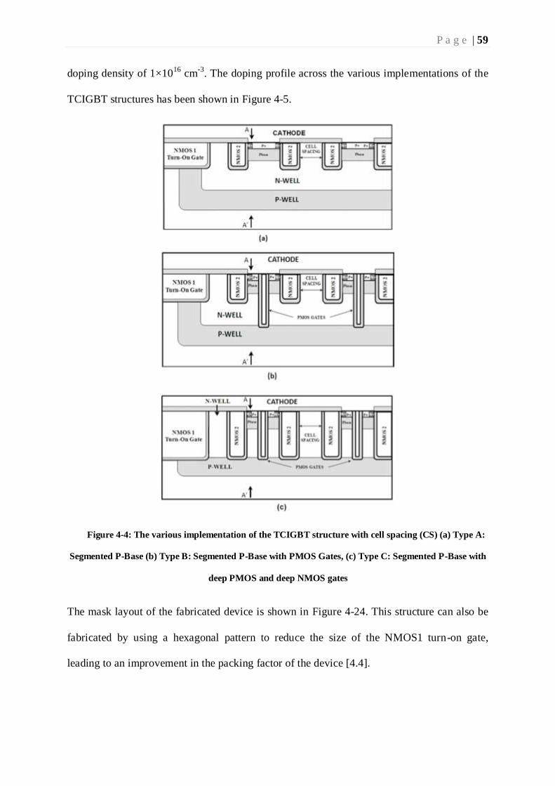
P a g e | 59
doping density of 1×10¹⁶
cm-3
. The doping profile across the various implementations of the
TCIGBT structures has been shown in Figure 4-5.
Figure 4-4: The various implementation of the TCIGBT structure with cell spacing (CS) (a) Type A:
Segmented P-Base (b) Type B: Segmented P-Base with PMOS Gates, (c) Type C: Segmented P-Base with
deep PMOS and deep NMOS gates
The mask layout of the fabricated device is shown in Figure 4-24. This structure can also be
fabricated by using a hexagonal pattern to reduce the size of the NMOS1 turn-on gate,
leading to an improvement in the packing factor of the device [4.4].
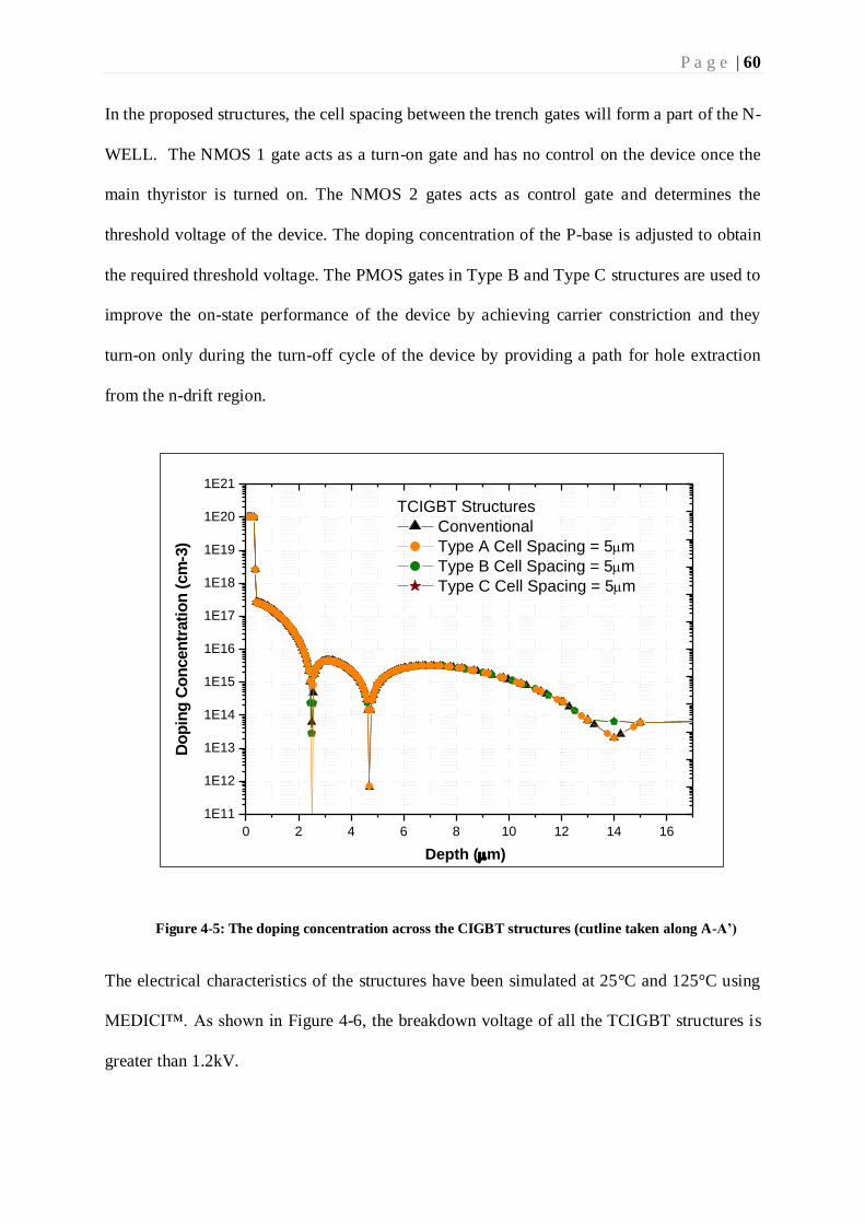
P a g e | 60
In the proposed structures, the cell spacing between the trench gates will form a part of the N-
WELL. The NMOS 1 gate acts as a turn-on gate and has no control on the device once the
main thyristor is turned on. The NMOS 2 gates acts as control gate and determines the
threshold voltage of the device. The doping concentration of the P-base is adjusted to obtain
the required threshold voltage. The PMOS gates in Type B and Type C structures are used to
improve the on-state performance of the device by achieving carrier constriction and they
turn-on only during the turn-off cycle of the device by providing a path for hole extraction
from the n-drift region.
Figure 4-5: The doping concentration across the CIGBT structures (cutline taken along A-A’)
The electrical characteristics of the structures have been simulated at 25°C and 125°C using
MEDICI™. As shown in Figure 4-6, the breakdown voltage of all the TCIGBT structures is
greater than 1.2kV.
0 2 4 6 8 10 12 14 16
1E11
1E12
1E13
1E14
1E15
1E16
1E17
1E18
1E19
1E20
1E21
TCIGBT Structures
Conventional
Type A Cell Spacing = 5m
Type B Cell Spacing = 5m
Type C Cell Spacing = 5m
Do
pin
g C
on
cen
trati
on
(cm
-3)
Depth (m)
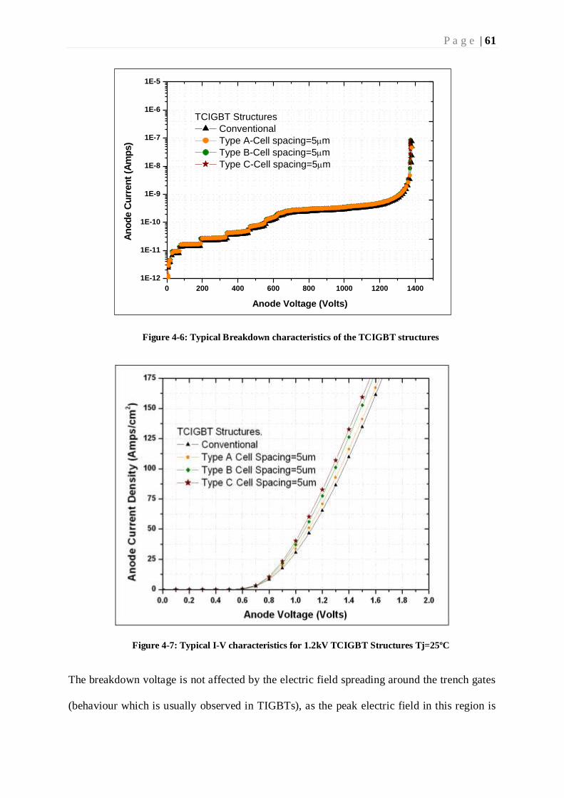
P a g e | 61
Figure 4-6: Typical Breakdown characteristics of the TCIGBT structures
Figure 4-7: Typical I-V characteristics for 1.2kV TCIGBT Structures Tj=25ºC
The breakdown voltage is not affected by the electric field spreading around the trench gates
(behaviour which is usually observed in TIGBTs), as the peak electric field in this region is
0 200 400 600 800 1000 1200 1400
1E-12
1E-11
1E-10
1E-9
1E-8
1E-7
1E-6
1E-5
TCIGBT Structures
Conventional
Type A-Cell spacing=5m
Type B-Cell spacing=5m
Type C-Cell spacing=5m
An
od
e C
urr
en
t (A
mp
s)
Anode Voltage (Volts)
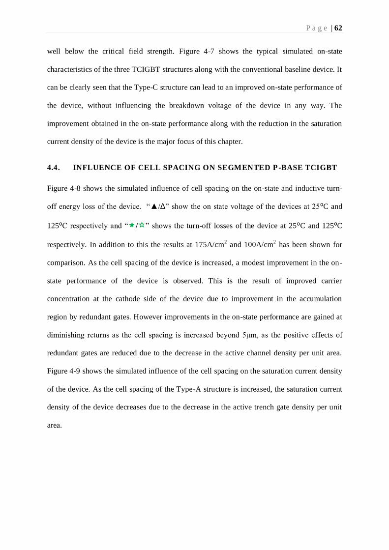
P a g e | 62
well below the critical field strength. Figure 4-7 shows the typical simulated on-state
characteristics of the three TCIGBT structures along with the conventional baseline device. It
can be clearly seen that the Type-C structure can lead to an improved on-state performance of
the device, without influencing the breakdown voltage of the device in any way. The
improvement obtained in the on-state performance along with the reduction in the saturation
current density of the device is the major focus of this chapter.
4.4. INFLUENCE OF CELL SPACING ON SEGMENTED P-BASE TCIGBT
Figure 4-8 shows the simulated influence of cell spacing on the on-state and inductive turn-
off energy loss of the device. “/Δ” show the on state voltage of the devices at 25⁰C and
125⁰C respectively and “ / ” shows the turn-off losses of the device at 25⁰C and 125⁰C
respectively. In addition to this the results at 175A/cm2 and 100A/cm
2 has been shown for
comparison. As the cell spacing of the device is increased, a modest improvement in the on-
state performance of the device is observed. This is the result of improved carrier
concentration at the cathode side of the device due to improvement in the accumulation
region by redundant gates. However improvements in the on-state performance are gained at
diminishing returns as the cell spacing is increased beyond 5μm, as the positive effects of
redundant gates are reduced due to the decrease in the active channel density per unit area.
Figure 4-9 shows the simulated influence of the cell spacing on the saturation current density
of the device. As the cell spacing of the Type-A structure is increased, the saturation current
density of the device decreases due to the decrease in the active trench gate density per unit
area.
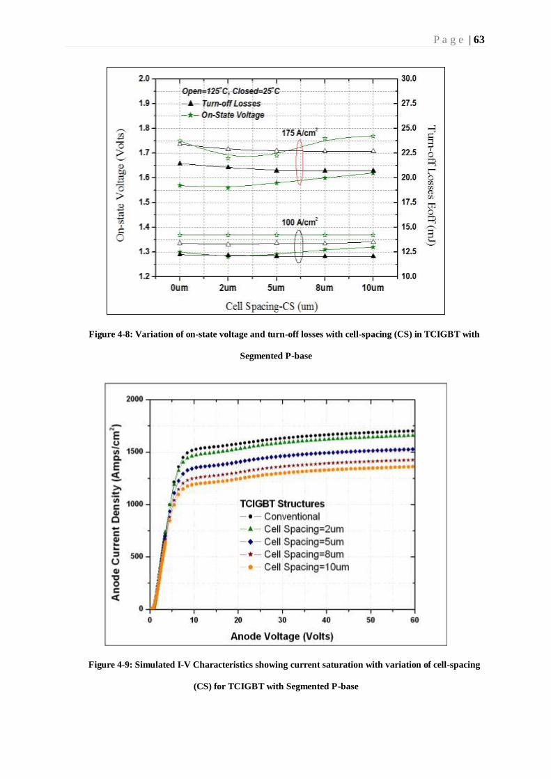
P a g e | 63
Figure 4-8: Variation of on-state voltage and turn-off losses with cell-spacing (CS) in TCIGBT with
Segmented P-base
Figure 4-9: Simulated I-V Characteristics showing current saturation with variation of cell-spacing
(CS) for TCIGBT with Segmented P-base
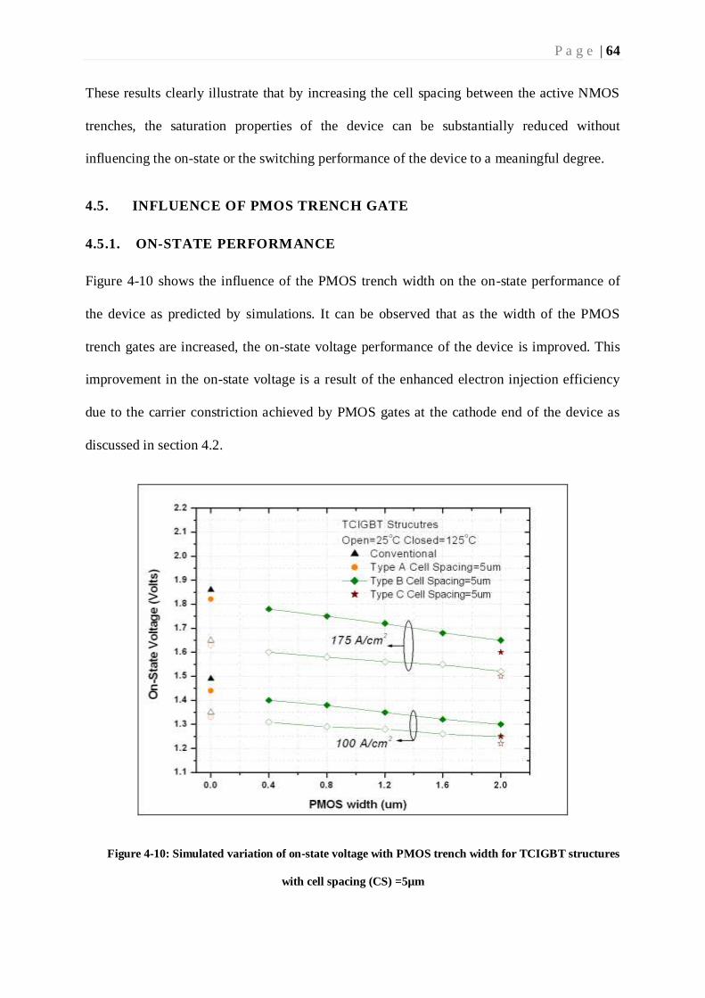
P a g e | 64
These results clearly illustrate that by increasing the cell spacing between the active NMOS
trenches, the saturation properties of the device can be substantially reduced without
influencing the on-state or the switching performance of the device to a meaningful degree.
4.5. INFLUENCE OF PMOS TRENCH GATE
4.5.1. ON-STATE PERFORMANCE
Figure 4-10 shows the influence of the PMOS trench width on the on-state performance of
the device as predicted by simulations. It can be observed that as the width of the PMOS
trench gates are increased, the on-state voltage performance of the device is improved. This
improvement in the on-state voltage is a result of the enhanced electron injection efficiency
due to the carrier constriction achieved by PMOS gates at the cathode end of the device as
discussed in section 4.2.
Figure 4-10: Simulated variation of on-state voltage with PMOS trench width for TCIGBT structures
with cell spacing (CS) =5µm
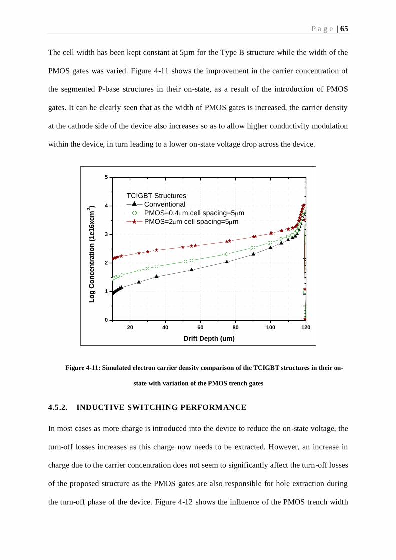
P a g e | 65
The cell width has been kept constant at 5µm for the Type B structure while the width of the
PMOS gates was varied. Figure 4-11 shows the improvement in the carrier concentration of
the segmented P-base structures in their on-state, as a result of the introduction of PMOS
gates. It can be clearly seen that as the width of PMOS gates is increased, the carrier density
at the cathode side of the device also increases so as to allow higher conductivity modulation
within the device, in turn leading to a lower on-state voltage drop across the device.
Figure 4-11: Simulated electron carrier density comparison of the TCIGBT structures in their on-
state with variation of the PMOS trench gates
4.5.2. INDUCTIVE SWITCHING PERFORMANCE
In most cases as more charge is introduced into the device to reduce the on-state voltage, the
turn-off losses increases as this charge now needs to be extracted. However, an increase in
charge due to the carrier concentration does not seem to significantly affect the turn-off losses
of the proposed structure as the PMOS gates are also responsible for hole extraction during
the turn-off phase of the device. Figure 4-12 shows the influence of the PMOS trench width
20 40 60 80 100 120
0
1
2
3
4
5
TCIGBT Structures
Conventional
PMOS=0.4m cell spacing=5m
PMOS=2m cell spacing=5m
Lo
g C
on
cen
trati
on
(1e16xcm
-3)
Drift Depth (um)
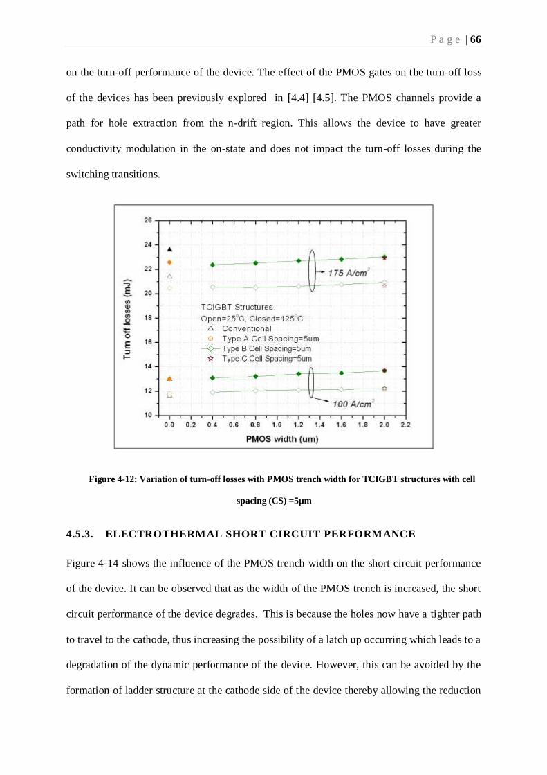
P a g e | 66
on the turn-off performance of the device. The effect of the PMOS gates on the turn-off loss
of the devices has been previously explored in [4.4] [4.5]. The PMOS channels provide a
path for hole extraction from the n-drift region. This allows the device to have greater
conductivity modulation in the on-state and does not impact the turn-off losses during the
switching transitions.
Figure 4-12: Variation of turn-off losses with PMOS trench width for TCIGBT structures with cell
spacing (CS) =5µm
4.5.3. ELECTROTHERMAL SHORT CIRCUIT PERFORMANCE
Figure 4-14 shows the influence of the PMOS trench width on the short circuit performance
of the device. It can be observed that as the width of the PMOS trench is increased, the short
circuit performance of the device degrades. This is because the holes now have a tighter path
to travel to the cathode, thus increasing the possibility of a latch up occurring which leads to a
degradation of the dynamic performance of the device. However, this can be avoided by the
formation of ladder structure at the cathode side of the device thereby allowing the reduction
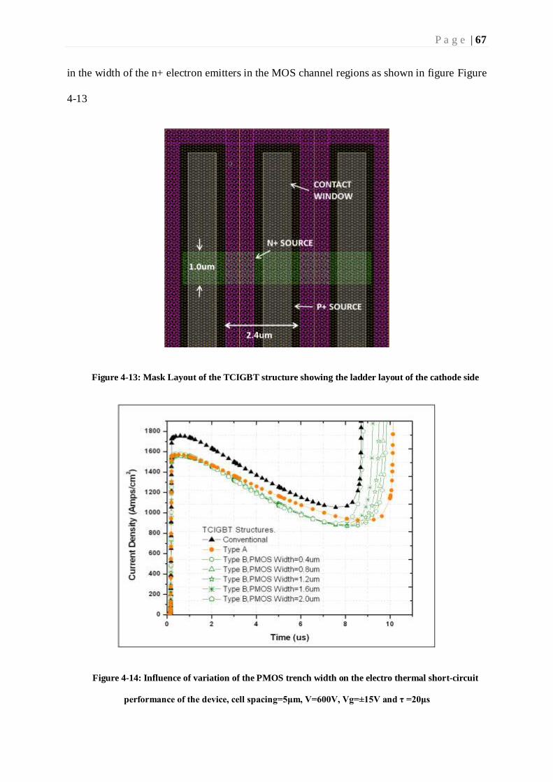
P a g e | 67
in the width of the n+ electron emitters in the MOS channel regions as shown in figure Figure
4-13
Figure 4-13: Mask Layout of the TCIGBT structure showing the ladder layout of the cathode side
Figure 4-14: Influence of variation of the PMOS trench width on the electro thermal short-circuit
performance of the device, cell spacing=5μm, V=600V, Vg=±15V and τ =20μs
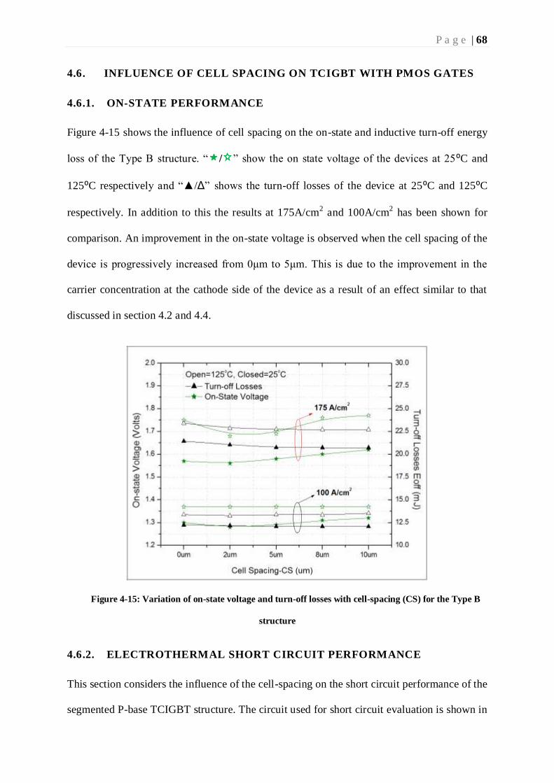
P a g e | 68
4.6. INFLUENCE OF CELL SPACING ON TCIGBT WITH PMOS GATES
4.6.1. ON-STATE PERFORMANCE
Figure 4-15 shows the influence of cell spacing on the on-state and inductive turn-off energy
loss of the Type B structure. “ / ” show the on state voltage of the devices at 25⁰C and
125⁰C respectively and “/Δ” shows the turn-off losses of the device at 25⁰C and 125⁰C
respectively. In addition to this the results at 175A/cm2 and 100A/cm
2 has been shown for
comparison. An improvement in the on-state voltage is observed when the cell spacing of the
device is progressively increased from 0μm to 5μm. This is due to the improvement in the
carrier concentration at the cathode side of the device as a result of an effect similar to that
discussed in section 4.2 and 4.4.
Figure 4-15: Variation of on-state voltage and turn-off losses with cell-spacing (CS) for the Type B
structure
4.6.2. ELECTROTHERMAL SHORT CIRCUIT PERFORMANCE
This section considers the influence of the cell-spacing on the short circuit performance of the
segmented P-base TCIGBT structure. The circuit used for short circuit evaluation is shown in

P a g e | 69
Figure 4-16. During the short circuit phase, the current in the device under test (DUT) is
limited by the saturation properties of the device. The power dissipated (PD) by the device
can thus be established from:
𝑃𝐷 = 𝐽𝑆𝐴𝑇 ∗ 𝑉𝐴 ….. (4.9)
Figure 4-16: Typical circuit used to evaluate the short-circuit performance of the TCIGBT
This constant power dissipated into the device will result in heating of the device. When the
temperature rise within the device reaches a critical value, the device would fail destructively,
at which point in-built potential becomes zero [4.6]. The time duration for the device to
withstand short circuit is thus found to be.
𝑡𝑠𝑐 = ((𝑇𝐶𝑅 − 𝑇𝐻𝑆) ∗ 𝑊𝑆𝑖 ∗ 𝐶𝑉)
(𝐽𝑆𝐴𝑇 ∗ 𝑉𝐴)⁄ ….. (4.10)
Where, TCR=Critical value of temperature, THS=Heat sink temperature, WSi= Thickness of
wafer, CV=Volumetric specific heat, JSAT = Saturation current density, VA=Anode DC
Supply. Figure 4-17 shows a comparison of the short circuit durations of the structures with
variation of cell-spacing. It is observed that the TCIGBT with the segmented P-base has

P a g e | 70
improved short circuit performance without degradation in its Eoff-Vce(sat) Trade-off. This
is a consequence of its saturation current level being some 23% lower than that of a
conventional TCIGBT which means that the rate of heat generation and temperature rise
would be markedly slower than a conventional TCIGBT structure.
Figure 4-17: Influence of cell spacing (CS) on the electro thermal short circuit performance of the
segmented P-Base TCIGBT structure, V=600V, Vg=±15V and τ =20μs
4.7. INFLUENCE OF DEEP NMOS AND PMOS TRENCH GATES
The influence of the deep NMOS and PMOS trench gates on the on-state performance is seen
in Figure 4-7 previously. The segmented P-base structure with deep NMOS trenches tends to
exhibit a lower on-state voltage as compared to the shallow NMOS trench devices. This is
because more electrons are injected during the turn-on phase. Figure 4-18 and Figure 4-19
shows the current flow lines in the Type B and Type C structures. Figure 4-20 shows the
electron concentration in the various TCIGBT structures when they are operated in their on-

P a g e | 71
state. It can be clearly observed that the Type C structure facilitates the improvement in the
carrier density at the cathode side of the device, leading to an improved on-state performance.
Figure 4-18: Predicted current flow lines in the segmented P-Base TCIGBT structure with PMOS
trench gates
Figure 4-19: Predicted current flow lines in the segmented P-Base TCIGBT structures with deep
NMOS and PMOS trench gates

P a g e | 72
Figure 4-20: Electron carrier density of the various TCIGBT structures in their on-state along A-A’
4.7.1. PERFORMANCE TRADE OFF
A model of a standard chopper circuit was used to calculate switching losses of the TCIGBT
structures. Figure 4-21 and Figure 4-22 shows the simulated Vce(sat)-Eoff trade-off curves at
25°C and 125°C respectively. The segmented P-base Structure with deep NMOS trenches
reduces the turn-off losses of the device by 23% and 25% for 100A/cm2 and 175A/cm
2
respectively. The results shown below clearly show that the Type B and Type C structure
offer a better performance trade off as compare to the Conventional structure. This is due to
the result of an increased conductivity modulation at the cathode end of the device while
using the PMOS gates for turn-off. In addition to this it is also observed that the use of
segmented P-base can also help in reducing the saturation current density of the device as the
active cell per unit area decreases. This happen without having an adverse impact on the on-
state voltage of the device. It is also observed that the Type C structure might simply the
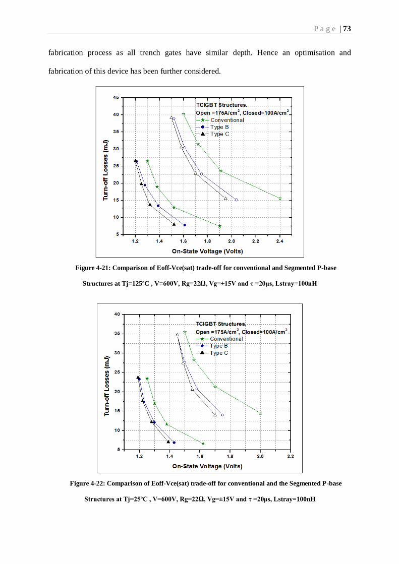
P a g e | 73
fabrication process as all trench gates have similar depth. Hence an optimisation and
fabrication of this device has been further considered.
Figure 4-21: Comparison of Eoff-Vce(sat) trade-off for conventional and Segmented P-base
Structures at Tj=125ºC , V=600V, Rg=22Ω, Vg=±15V and τ =20μs, Lstray=100nH
Figure 4-22: Comparison of Eoff-Vce(sat) trade-off for conventional and the Segmented P-base
Structures at Tj=25ºC , V=600V, Rg=22Ω, Vg=±15V and τ =20μs, Lstray=100nH

P a g e | 74
4.8. DEVICE FABRICATION
Having explored many aspects of performance of various devices by simulation, this section
describes the fabrication of a segmented P-base TCIGBT structure with deep NMOS and
PMOS gates. The typical process fabrication steps for TCIGBT structures are listed in Table
4-1. The first few steps involve the formation of the floating deep P-WELL/N-WELL
regions.
Table 4-1: Proposed process for the 1.2kV segmented P-base TCIGBT structures
Starting material N+ Substrate
P-WELL and N-WELL regions are selectively implanted
and annealed to form the clusters.
P-base regions are formed at the same time as the field
rings, which are to support breakdown voltage in the
termination area
N+ region is selectively implanted
The trench gate regions are etched
Gate oxides and polysilicon layers are grown
P+ is selectively implanted and annealed at high
temperatures.
Contact windows are etched and metal is deposited.
Backside of the wafer is thinned by grinding and is
chemically etched.
N+ and P+ are implanted as required to form the buffer and
collector regions respectively.
Anode Metal is deposited by evaporation.
Annealed at a relatively low temperature.
The P-base regions are then implanted inside and outside the MOS clusters to form the P-
base and termination regions, respectively. The floating P-base regions outside the TCIGBT
clusters act as field termination rings for the TCIGBT structures and prevent the surface
electric field from exceeding the critical field strength. The n+ regions are then selectively
implanted. The trench gates are formed by etching into the silicon area followed by the

P a g e | 75
growth of poly-silicon to form the control and turn-on trench gates, respectively. The gates
which operate as turn-on gate are formed by the same trenches that act as control gates and
this is illustrated in Figure 4-23. The p+ regions are then selectively implanted and the
contact windows are etched and metallised to form the cathode side of the TCIGBT structure.
Figure 4-23: The cross section schematic of the TCIGBT structure
The formation of the anode region is achieved by first grinding the wafer (thinning) followed
by boron and phosphorus implantation to form the buffer and the P+ regions, respectively.
The last step involves the deposition of the anode metal by evaporation. The mask layout for
the segmented TCIGBT structure is shown in Figure 4-24. The cell spacing is adjusted to
form the segmented PBASE structure. The n+ and p+ implants are controlled, based on the
minimum design rules. The MOS cells are designed to meet the minimum cell dimensions
that ensure that the channel density is not compromised substantially.
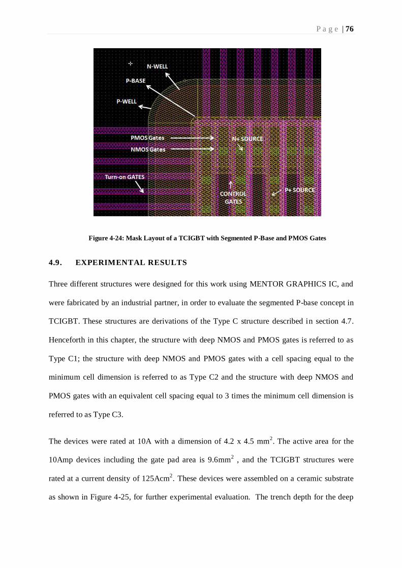
P a g e | 76
Figure 4-24: Mask Layout of a TCIGBT with Segmented P-Base and PMOS Gates
4.9. EXPERIMENTAL RESULTS
Three different structures were designed for this work using MENTOR GRAPHICS IC, and
were fabricated by an industrial partner, in order to evaluate the segmented P-base concept in
TCIGBT. These structures are derivations of the Type C structure described in section 4.7.
Henceforth in this chapter, the structure with deep NMOS and PMOS gates is referred to as
Type C1; the structure with deep NMOS and PMOS gates with a cell spacing equal to the
minimum cell dimension is referred to as Type C2 and the structure with deep NMOS and
PMOS gates with an equivalent cell spacing equal to 3 times the minimum cell dimension is
referred to as Type C3.
The devices were rated at 10A with a dimension of 4.2 x 4.5 mm2. The active area for the
10Amp devices including the gate pad area is 9.6mm2 , and the TCIGBT structures were
rated at a current density of 125Acm2. These devices were assembled on a ceramic substrate
as shown in Figure 4-25, for further experimental evaluation. The trench depth for the deep

P a g e | 77
NMOS and PMOS gates is designed to penetrate the Pwell-Nwell junction and is therefore
~6µm deep.
Figure 4-25: TCIGBT devices assembled on a ceramic substrate
4.9.1. MEASURED ON-STATE PERFORMANCE
Figure 4-26 and Figure 4-27 show that the TCIGBT structures have a snap-back free turn-on,
and its on-state behaviour exhibits a positive temperature coefficient at higher temperatures.
Figure 4-26: Typical experimental CIGBT on-state I(V) at 25ºC Vg=15V
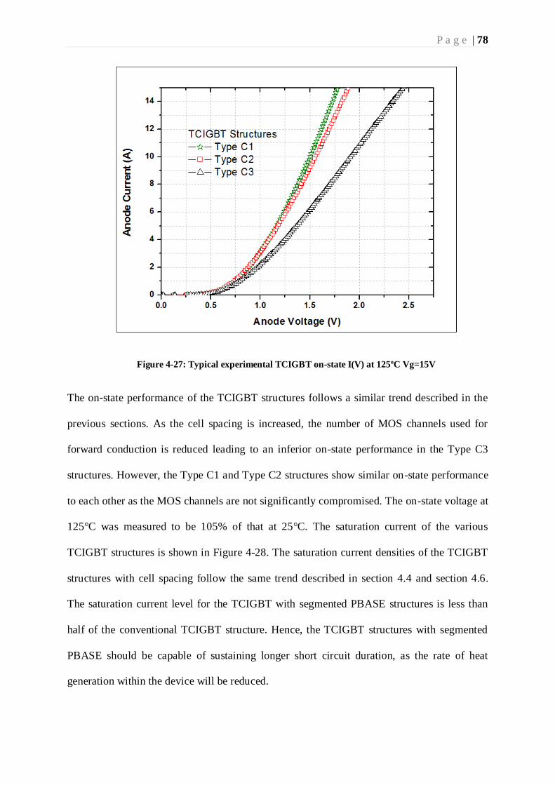
P a g e | 78
Figure 4-27: Typical experimental TCIGBT on-state I(V) at 125ºC Vg=15V
The on-state performance of the TCIGBT structures follows a similar trend described in the
previous sections. As the cell spacing is increased, the number of MOS channels used for
forward conduction is reduced leading to an inferior on-state performance in the Type C3
structures. However, the Type C1 and Type C2 structures show similar on-state performance
to each other as the MOS channels are not significantly compromised. The on-state voltage at
125°C was measured to be 105% of that at 25°C. The saturation current of the various
TCIGBT structures is shown in Figure 4-28. The saturation current densities of the TCIGBT
structures with cell spacing follow the same trend described in section 4.4 and section 4.6.
The saturation current level for the TCIGBT with segmented PBASE structures is less than
half of the conventional TCIGBT structure. Hence, the TCIGBT structures with segmented
PBASE should be capable of sustaining longer short circuit duration, as the rate of heat
generation within the device will be reduced.
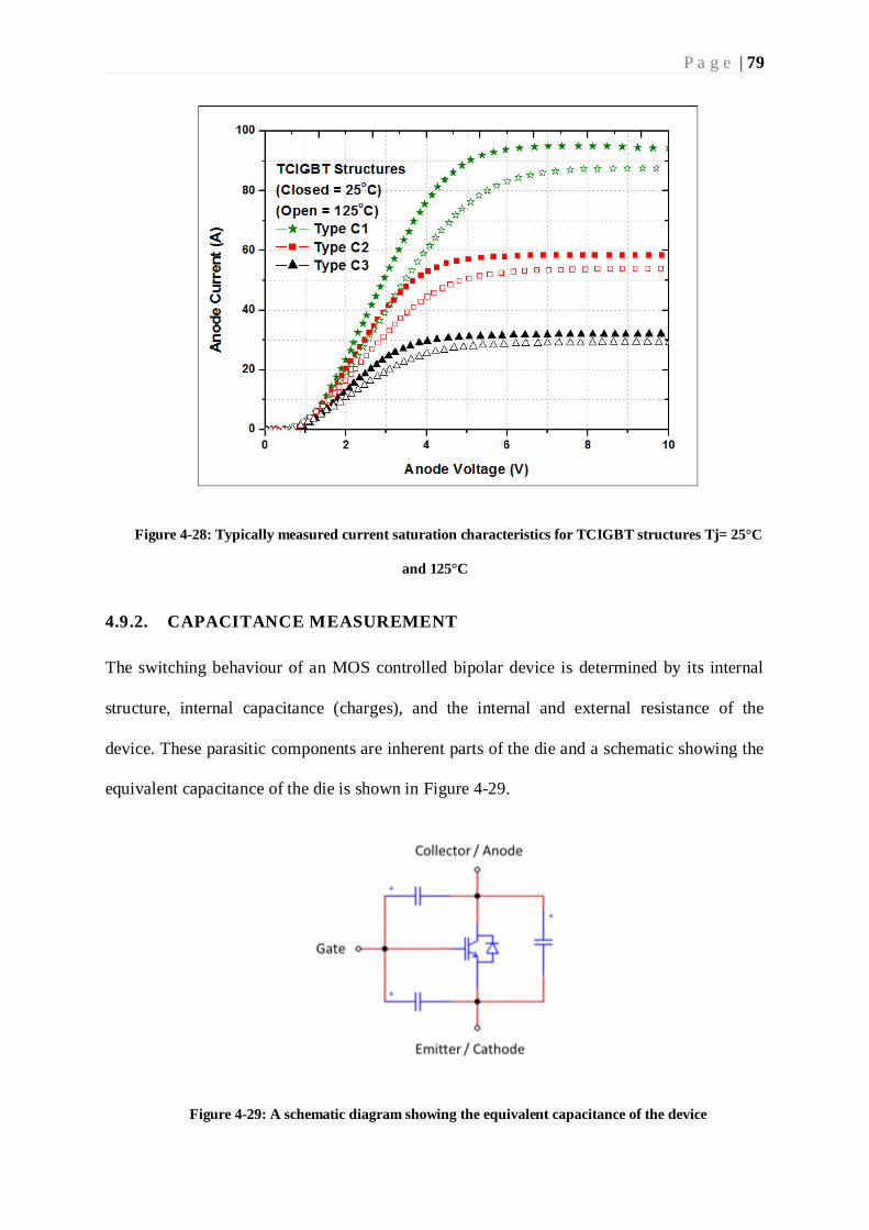
P a g e | 79
Figure 4-28: Typically measured current saturation characteristics for TCIGBT structures Tj= 25°C
and 125°C
4.9.2. CAPACITANCE MEASUREMENT
The switching behaviour of an MOS controlled bipolar device is determined by its internal
structure, internal capacitance (charges), and the internal and external resistance of the
device. These parasitic components are inherent parts of the die and a schematic showing the
equivalent capacitance of the die is shown in Figure 4-29.
Figure 4-29: A schematic diagram showing the equivalent capacitance of the device
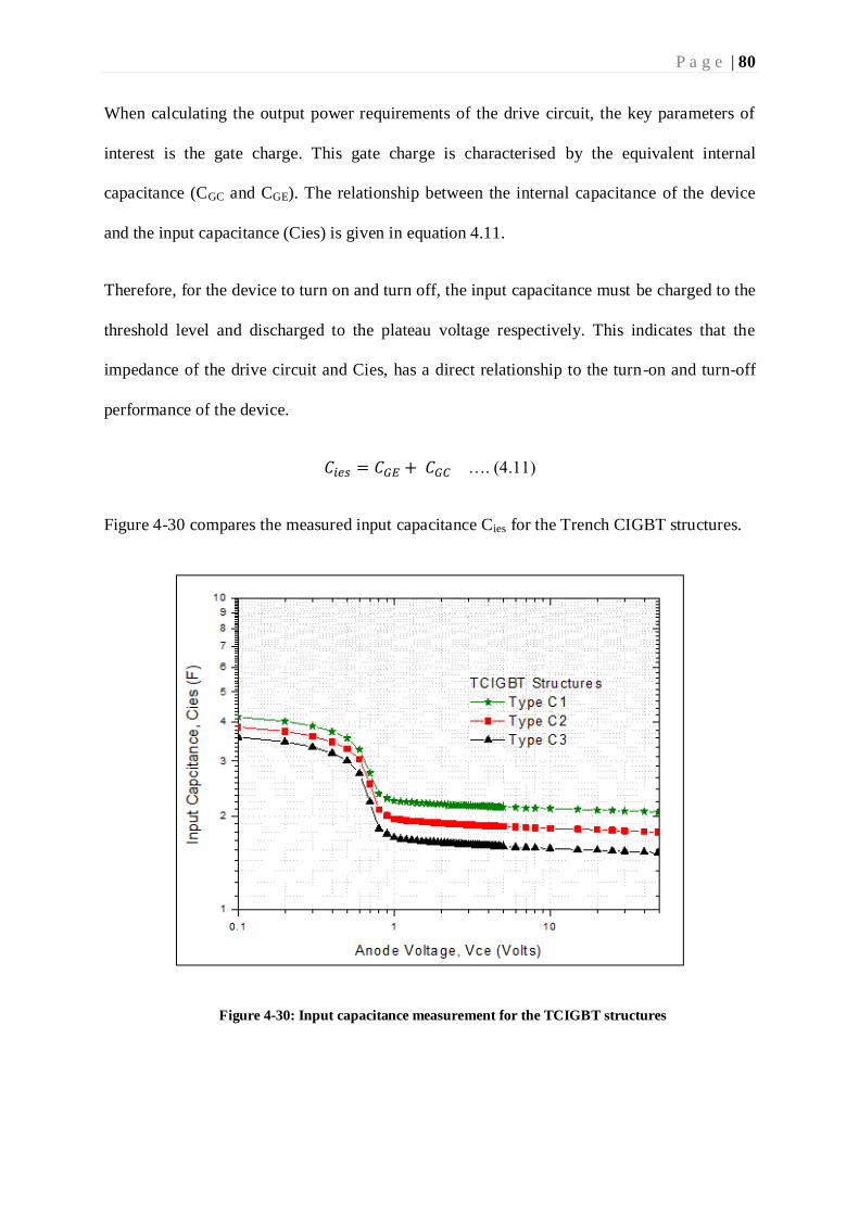
P a g e | 80
When calculating the output power requirements of the drive circuit, the key parameters of
interest is the gate charge. This gate charge is characterised by the equivalent internal
capacitance (CGC and CGE). The relationship between the internal capacitance of the device
and the input capacitance (Cies) is given in equation 4.11.
Therefore, for the device to turn on and turn off, the input capacitance must be charged to the
threshold level and discharged to the plateau voltage respectively. This indicates that the
impedance of the drive circuit and Cies, has a direct relationship to the turn-on and turn-off
performance of the device.
𝐶𝑖𝑒𝑠 = 𝐶𝐺𝐸 + 𝐶𝐺𝐶 …. (4.11)
Figure 4-30 compares the measured input capacitance Cies for the Trench CIGBT structures.
Figure 4-30: Input capacitance measurement for the TCIGBT structures

P a g e | 81
The segmented P-Base structures (Type C2 and Type C3 structures) show a lower value of
Cies as compared to the Type C1 structures. Hence, the segmented P-Base structures will be
easier to drive, which should in turn manifest itself in shorter switching times and reduced
switching losses as compared to the Type C1 structures.
Figure 4-31: Measured Output and Transfer capacitance for the TCIGBT structures
The use of segmented P-base structure has very little impact on the reverse transfer
capacitance and the output capacitance as shown in Figure 4-31. Hence, these capacitances
do not affect the switching performance between the TCIGBT structures to any significant
degree.
4.9.3. PERFORMANCE TRADE OFF
The Vce(sat)/Eoff trade-off shows that the segmented P-base structures with deep NMOS and
PMOS gates (Type C2 and Type C3) exhibit an improved trade-off performance as compared
to the TCIGBT structure with deep NMOS and PMOS gates (Type C1). This can be
attributed to the fact that the segmented PBASE structures have a lower input capacitance. In
addition to this, as the number of MOS channels per unit area is higher for the Type C1
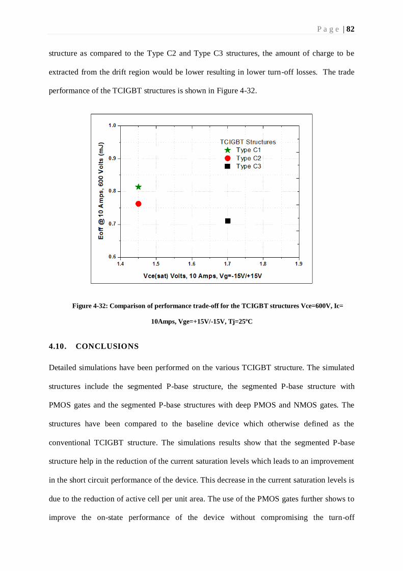
P a g e | 82
structure as compared to the Type C2 and Type C3 structures, the amount of charge to be
extracted from the drift region would be lower resulting in lower turn-off losses. The trade
performance of the TCIGBT structures is shown in Figure 4-32.
Figure 4-32: Comparison of performance trade-off for the TCIGBT structures Vce=600V, Ic=
10Amps, Vge=+15V/-15V, Tj=25ºC
4.10. CONCLUSIONS
Detailed simulations have been performed on the various TCIGBT structure. The simulated
structures include the segmented P-base structure, the segmented P-base structure with
PMOS gates and the segmented P-base structures with deep PMOS and NMOS gates. The
structures have been compared to the baseline device which otherwise defined as the
conventional TCIGBT structure. The simulations results show that the segmented P-base
structure help in the reduction of the current saturation levels which leads to an improvement
in the short circuit performance of the device. This decrease in the current saturation levels is
due to the reduction of active cell per unit area. The use of the PMOS gates further shows to
improve the on-state performance of the device without compromising the turn-off

P a g e | 83
performance. This is because the PMOS gates help in charge extraction during the turn-off
phase. Lastly it has been observed that the Deep NMOS and PMOS trench gates along with
the segmented P-base structures give rise to improved performance trade-off without
compromising the on-state voltage, the switching performance or the short-circuit
performance of the device. This is due to the optimised use of the N-well concentration. It is
also noted that as the trench gates are of equal depth, this structure simplifies the fabrication
process and leads to a reduction in the fabrication cost.
Following the simulation results a few variations of the TCIGBT structure with deep NMOS
and PMOS gates were fabricated and experiementally evaluated. The results obtained verify
the simulation results shown in this chapter. This work was done in collaboration with device
manufacturer. Hence a number of design rules were pre-defined in order to reduce the cost of
fabrication. However, the results clearly show the influence of the segmented P-base on the
fabricated structures. The reduction of the current saturation levels is observed and its impact
on the on-state voltage also follows the trend discussed in the simulations.

P a g e | 84
4.11. REFERENCES
[4.1] B. J. Baliga, Fundamentals of Power Semiconductor Devices: Springer, 2010. [4.2] M. Kitagawa, I. Omura, S. Hasegawa, T. Inoue, and A. Nakagawa, "A 4500 V
sinjection enhanced insulated gate bipolar transistor (IEGT) operating in a mode similar to a thyristor," in Electron Devices Meeting, 1993. IEDM '93. Technical Digest., International, 1993, pp. 679-682.
[4.3] E. M. Sankara Narayanan, M. R. Sweet, N. Luther-King, K. Vershinin, O. Spulber, M. M. De Souza, et al., "A novel, clustered insulated gate bipolar transistor for high power applications," in Semiconductor Conference, 2000. CAS 2000 Proceedings. International, 2000, pp. 173-181 vol.1.
[4.4] N. Luther-King, E. M. S. Narayanan, L. Coulbeck, A. Crane, and R. Dudley, "Comparison of Trench Gate IGBT and CIGBT Devices for Increasing the Power Density From High Power Modules," Power Electronics, IEEE Transactions on, vol. 25, pp. 583-591.
[4.5] L. Ngwendson and E. M. Sankara Narayanan, "Evaluation of 1.2kV Super Junction Trench-Gate Clustered Insulated Gate Bipolar Transistor (SJ-TCIGBT) " presented at the ISPSD'11, 2011.
[4.6] H. Hagino, J. Yamashita, A. Uenishi, and H. Haruguchi, "An experimental and numerical study on the forward biased SOA of IGBTs," Electron Devices, IEEE
Transactions on, vol. 43, pp. 490-500, 1996.

P a g e | 85
CHAPTER FIVE
Chapter 5
EVALUATION OF POWER DEVICES FOR A MULTILEVEL POWER
CONVERTER APPLICATION
5.1. INTRODUCTION
All power conversion applications use power semiconductor devices to convert, control and
manage electrical power. The need of efficient, reliable, high power and high temperature
conversions stages has increased the design challenges of developing high power converters.
The weight, size and cost of the power converters form some of the key criteria used to
determine the feasibility of using power conversion stages in aerospace and automotive
application. Figure 5-1 shows the expected development trend for power conversion stages
for a number of different applications [5.1]. Most aerospace and automotive applications tend
to target reductions in cost, weight and volume of the power conversion system while
maintaining or improving on the reliability and efficiency of the system.
Figure 5-1: Expected development trends for power converters [5.2]

P a g e | 86
As will be apparent from Figure 5-1, although there is marked upward trend with time, at any
given point there remains large variations in the power density achieved by the converter
depending on the type of power conversion stage and the application. In terms of the
influence of the application, a converter for a motor drive tends to be subject to very different
constraints vis-à-vis the requirements placed on a power converter for power bus/grid
provision. Power converters which are responsible for bus provision usually require large and
bulky filters to meet stringent power quality requirements, which tend to result in a reduction
in the power density of the converter as compared to power converters that are used for motor
drive applications. Even this limited example demonstrates that a comparison of power
converters solely on power density is potentially misleading without some context in terms of
the application requirements, the operating environment and the nature of the cooling
employed. In addition to this limitation, the power density figures quoted for high
performance converters often do not include allowance for the mass or volume of ancillary
systems that are required for the normal operation of the power converter, e.g. heat
exchangers, EMI filters, the DC-Link capacitors, external housing and the terminal
connectors. Very often, power density values are quoted solely in terms of the gross weight
of the bare minimum of components required to operate the power converter. Considering
power density values with such limited scope is not sufficient to fully understand or evaluate
the technology barriers to high power dense converter systems. Therefore one must consider
all the elements that form the converter system, viz: -
1. Power semiconductor module
2. Control circuits and Auxiliary systems (Protection circuits, Power supply units etc...)
3. Power level passive components (largely filter components)
4. Heat exchangers
5. Interconnections and packaging

P a g e | 87
A useful measure of gravimetric (ρm) or volumetric (ρv) power density of the converter is the
total output power divided by the weight or the volume of the entire system. In the case of a
system comprising n component/subsystems, these measures of power density can be
evaluated as: -
𝜌𝑚 =𝑃𝑂𝑢𝑡𝑝𝑢𝑡
∑ 𝑀𝑖𝑛𝑖=1
… . (5.1)
𝜌𝑣 =𝑃𝑂𝑢𝑡𝑝𝑢𝑡
∑ 𝑉𝑖𝑛𝑖=1
… . (5.2)
Where, POutput = Total power output of the converter, Mi = Mass of the component in
kilograms, Vi = Volume of the components in litres and n=is the number of components that
make up the converter. In order to optimise the gravimetric power density of the power
converter, one needs to concentrate on the elements beyond the power module and its
immediate heat sink, which tend to dominate the remainder of the volume and weight of the
system. It has been suggested in literature that the heat exchanger, the passive filters/ EMI
filters and the dc-link capacitor are the components usually responsible for compromising the
power density of the converter [5.3]. The key methods that can be employed to reduce the
size of these components are listed in Table 5-1. As seen in the table below, the use of -lower
loss switching devices either capable of switching at high frequencies and/or operating in a
different converter topology as compared to the standard 6 switch inverter offers scope to
reduce the size of the heat exchanger and passive components.
The focus of this chapter is to evaluate the merits of using GaN power devices within the
context of a power converter application in order to establish whether the potential of these
devices translates into corresponding benefits in the power density of converters, with
particular emphasis on using commercially available devices.

P a g e | 88
Table 5-1: Key methods used to allow reduction in power converter weight and size
Key Converter Components Mass and Volume Reduction Methods
Heat exchanger size
1. Use of low loss semiconductor devices.
2. Use of advanced thermal management
techniques.
3. High temperature operation of devices.
4. Use of other coolant & Heat exchanger
technologies
Passive/EMI filters
2. High switching frequency operation via
the use of low loss semiconductor
devices.
3. Use of multilevel converters
4. Improvements in material properties and
manufacturing methods.
5.2. CANDIDATE SEMICONDUCTOR DEVICE TECHNOLOGY
The selection of the semiconductor device technology for a given converter is usually
influenced by factors such as the nature of the application of the power converter, the
operating voltage and current, environmental and coolant constraints, and the reliability and
maturity of technology, which might for example include deployment in safety critical
applications.
5.2.1. SILICON BASED DEVICE TECHNOLOGY
Silicon based power devices are preferred in an overwhelming majority of power converters
as they offer a more mature device technology and a well understood and proven reliability
behaviour. In addition, in many cases, the use of Silicon power devices allows the risk
associated to the power converter development to be reduced. The range of Silicon devices
for power conversion include Diodes, Thyristors, Triac, Gate turn-off Thyristors (GTO),
Integrated Gate Commutated Thyristor (IGCT), Metal-Oxide Semiconductor Field Effect

P a g e | 89
Transistors (MOSFET), Insulated Gate Bipolar Transistors (IGBT), Bipolar Junction
Transistors (BJT). Table 5-2 shows representative characteristics of these device types, while
Figure 5-2 shows the application scope of these technologies in terms of power levels and
operational frequency. As illustrated by both, Table 5-2 and Figure 5-2, there is no single
device technology that is capable of operating over the full range of current and voltage
rating while offering the best performance match.
Table 5-2: Typical Power device characteristics [5.4]
Property Thyristor
(SCR)
Triac GTO IGCT MOSFET IGBT
Self-commutation
ability
No No Yes Yes Yes Yes
Maximum rms
current ratings (A)
5000 400 2000 1700 300 2400
Maximum Voltage
ratings (V)
12000 1200 6000 5500 1500 6500
Maximum
Switching VA
ratings
30MVA 240kVA 30MVA 12MVA 30kVA 4MVA
Maximum
operation junction
temperature
125⁰C 125⁰C 125⁰C 115⁰C 175⁰C 175⁰C
On-state losses Low Low Medium Low High* Medium
Switching Losses Very High High Very
High Medium Very Low Low
Turn-on ability
Medium (di/dt limit)
Medium (di/dt limit)
Medium (di/dt limit)
Medium (di/dt limit)
Very good Very good
Turn-off ability
None via gate
Medium Poor – slow and
lossy
Good Very good Very good
Minimum on or off
time
10 – 100µs 10 – 50µs 10 – 50µs 10µs <100ns <1µs
Maximum
switching
frequency
A few 100
Hz
A few 100
Hz
A few
100 Hz
A few 100
Hz
>50kHz <25kHz
Control of
switching time
No No No No Yes Yes
Drive circuit power Low Medium High High Low Low
Drive circuit
complexity
Low Medium High High Low Low
Series and parallel
operation
Yes Yes Difficult to series
or parallel
Easy to series,
difficult to parallel
Yes Depending on type of
IGBT technology
. * Voltage and current dependent.

P a g e | 90
Figure 5-2: Application range of discrete power semiconductor device technologies in Silicon [5.5]
Power MOSFETs allow very high switching frequencies due to their method of conduction
(Majority Carriers only), and commercially available MOSFETS have limited blocking
voltage capability and high losses in the forward conduction mode for all but modest voltage
& current ratings.
5.2.1.1. SILICON POWER MOSFETS
As described in the above section, Silicon power MOSFETs are more preferred for a low to
medium power and high frequency operation. This section discusses the operation of a power
MOSFET and its main limitation. The basic structure of a power MOSFET is shown in cross-
section in Figure 5-3. Power MOSFETs have a drift region which is used to support the
breakdown characteristics of the device and a buffer region that can be used to reduce the
forward voltage drop of the device during the forward conduction mode.
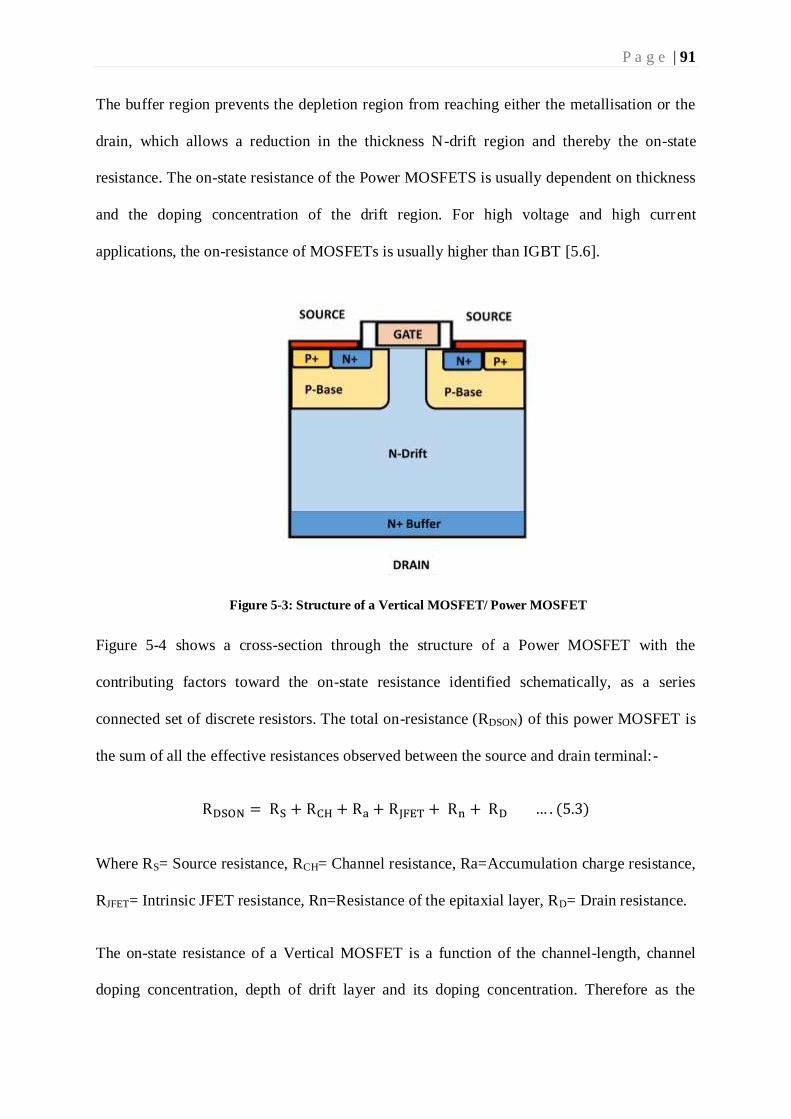
P a g e | 91
The buffer region prevents the depletion region from reaching either the metallisation or the
drain, which allows a reduction in the thickness N-drift region and thereby the on-state
resistance. The on-state resistance of the Power MOSFETS is usually dependent on thickness
and the doping concentration of the drift region. For high voltage and high current
applications, the on-resistance of MOSFETs is usually higher than IGBT [5.6].
Figure 5-3: Structure of a Vertical MOSFET/ Power MOSFET
Figure 5-4 shows a cross-section through the structure of a Power MOSFET with the
contributing factors toward the on-state resistance identified schematically, as a series
connected set of discrete resistors. The total on-resistance (RDSON) of this power MOSFET is
the sum of all the effective resistances observed between the source and drain terminal:-
RDSON = RS + RCH + Ra + RJFET + Rn + RD … . (5.3)
Where RS= Source resistance, RCH= Channel resistance, Ra=Accumulation charge resistance,
RJFET= Intrinsic JFET resistance, Rn=Resistance of the epitaxial layer, RD= Drain resistance.
The on-state resistance of a Vertical MOSFET is a function of the channel-length, channel
doping concentration, depth of drift layer and its doping concentration. Therefore as the
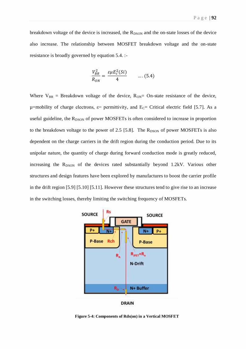
P a g e | 92
breakdown voltage of the device is increased, the RDSON and the on-state losses of the device
also increase. The relationship between MOSFET breakdown voltage and the on-state
resistance is broadly governed by equation 5.4. :-
𝑉𝐵𝑅2
𝑅𝑂𝑁
= 𝜀𝜇𝐸𝑐
2(𝑆𝑖)
4 … . (5.4)
Where VBR = Breakdown voltage of the device, RON= On-state resistance of the device,
µ=mobility of charge electrons, ε= permittivity, and EC= Critical electric field [5.7]. As a
useful guideline, the RDSON of power MOSFETs is often considered to increase in proportion
to the breakdown voltage to the power of 2.5 [5.8]. The RDSON of power MOSFETs is also
dependent on the charge carriers in the drift region during the conduction period. Due to its
unipolar nature, the quantity of charge during forward conduction mode is greatly reduced,
increasing the RDSON of the devices rated substantially beyond 1.2kV. Various other
structures and design features have been explored by manufactures to boost the carrier profile
in the drift region [5.9] [5.10] [5.11]. However these structures tend to give rise to an increase
in the switching losses, thereby limiting the switching frequency of MOSFETs.
Figure 5-4: Components of Rds(on) in a Vertical MOSFET

P a g e | 93
Figure 5-5 shows the variation of specific on-resistance of commercially available Silicon
MOSFETs with the breakdown voltage. As the required breakdown voltage ratings of Power
MOSFETs are reduced, the lateral MOS structures become more favourable since they allow
the removal of the drift and the buffer regions leading to a decrease in on-state resistance
(RDSON). The on-state resistance for these MOSFETs now depend only on the channel
dimension (length and width) and its doping concentration. The channel resistance becomes
the limiting factor on the on-resistance of the device performance. However as the breakdown
voltages of these devices are much lower as compared to vertical structures (typically limited
to <200V) , it may be necessary to consider alternative converter topologies, most notably
the series connection of a number of devices so as to cater for a similar voltage application as
compared to standard vertical power MOSFETs. The basic structure of a lateral MOSFET is
shown in Figure 5-6.
Figure 5-5: The specific on resistance (RDS(ON-SP)) of MOSFETs with increase in their voltage ratings
[5.2]

P a g e | 94
Figure 5-6: Basic Structure of a Lateral MOSFET
The main disadvantage of lateral structures as compared to vertical structures is that they
have lower current density as the effective area of silicon is underutilised. The vertical region
of Silicon is only used to support the breakdown voltage and does not take part in current
conduction. However they can still be switched at very high frequencies, allowing the size of
the passive elements to be reduced while improving the power density.
5.2.2. GALLIUM NITRIDE (GAN) BASED DEVICE TECHNOLOGY
Figure 5-7 shows the specific on-resistance as a function of the breakdown voltage for a
number of different materials and technologies. This data was collected from [5.8]. It can be
clearly seen that for a similar voltage rating, GaN material offers a much lower specific
RDS(ON-SP) as compared to Silicon or Silicon Carbide. This offers scope for fabricated GaN
devices to be smaller as compared to their Silicon or Silicon Carbide counterparts for a given
breakdown voltage.
GaN based power devices are usually available in a HEMT structure (High Electron Mobility
Transistor), a structure first described by T.Mimura et.al in 1975. This structure, a cross-
section of which is shown in Figure 5-8, demonstrates an unusually high electron mobility

P a g e | 95
which is often referred to as a 2-D electron gas (2DEG). The presence of a 2DEG gas near
the interface of the GaN and AlGaN heterostructure interface is responsible for the low on-
state performance of the device. The GaN based HEMT structures are normally on-structures
due to the large polarisation-induced charge carried in the AlGaN/GaN interface.
Similar to the Silicon MOSFET structure, the HEMT structure in its basic form has three
terminals, viz. source, drain and gate. The source and drain terminals pierce through the top
AlGaN layer to from an ohmic contact with the 2DEG- electron gas layer. This creates a
short between the drain and source terminal, resulting in a normally-on device. In order to
turn-off the device, a gate electrode is place on the top of the AlGaN layer such that a
Schottky contact is formed in the top surface. When a negative voltage is applied to this
contact, the Schottky barrier becomes reverse biased and the electrons underneath the gate
region are depleted which in turn allows the device to turn-off.
Figure 5-7: Ron*A relation with designed blocking voltage of Si, SiC and GaN-Mosfet and JFET
devices as well as for bipolar IGBT devices [5.8]

P a g e | 96
Figure 5-8: A typical AlGaN/GaN HEMT structure with three metal-semiconductor contacts
This type of device is usually referred to as a depletion mode HEMT structure. In most
applications, a normally-off or enhancement mode device with a positive threshold voltage
(Vth) is preferred over a depletion mode structure. This is to ensure the safe operation of the
power converter during start up and during any failure of the control electronics or other
componets. Various methods have been proposed in literature to develop an enhancement
mode HEMT structure. The most common methods described in the literature are given
below [5.12] .
1. Cascode configuration.
2. Fluorine Plasma Implantation. [5.13]
3. Recessed Gate Structure.[5.14]
4. Gate Injection Transistor Configuration. [5.15]
5. PN Junction Gates[5.16]
In early 2009, a few companies offered enhancement mode GaN devices with a view to
catering to the power conversion market. A cross section of this structure is shown in Figure
5-9. Unlike Silicon devices, these devices are made by depositing a highly resistive layer of
gallium nitride (GaN) over silicon (Si). A thin layer of Aluminium Nitride is used for
Isolation between the GaN and Silicon Layers. An electron generating material is then
applied to the GaN layer producing an abundance of electrons near the top of the underlying

P a g e | 97
GaN. The further processing of GaN layers assists in the formation of a depletion region
under the gate.
Figure 5-9: Structure of an enhancement mode GaN Power transistor [5.17]
Under normal conditions, theses device are in a normally off-state. However when a positive
voltage is applied to the gate relative to the source, a field effect is created which attracts
electrons to form a bidirectional channel between drain and source. The maximum ratings of
these commercially available GaN devices are 200V/12A). Hence although they offer a
potentially attractive device for power conversion, their limited voltage capability dictates
that different topologies of power converters would need to be considered in order to cater to
higher voltage applications. The breakdown voltage of GaN devices is usually increased by
increasing the distance between the gate and the drain contacts and, since the resistivity of the
GaN electron pool is very low, the impact of increasing the breakdown voltage of the on-
resistance is also very low. The relationship between breakdown voltage to Ron for these
devices is given in equation 5.5 [5.18].
𝑉𝐵𝑅2 = 𝑅𝑂𝑁 ∗ 𝑞𝑛𝑠µ (𝐸𝐶
2 𝐸𝑝2) … . (5.5)
Where 𝑉𝐵𝑅= Device breakdown voltage, 𝑅𝑂𝑁= On-state resistance, q = electron elementary
charge, 𝑛𝑠= 2DEG density of channel, µ= Mobility of carriers, 𝐸𝐶 = Critical Electric Field
GaN (Volts/cm), 𝐸𝑃= Polarisation Field. Therefore as the distance between the source and
drain terminals are increased, the effect on on-state resistance is minimal. The breakdown
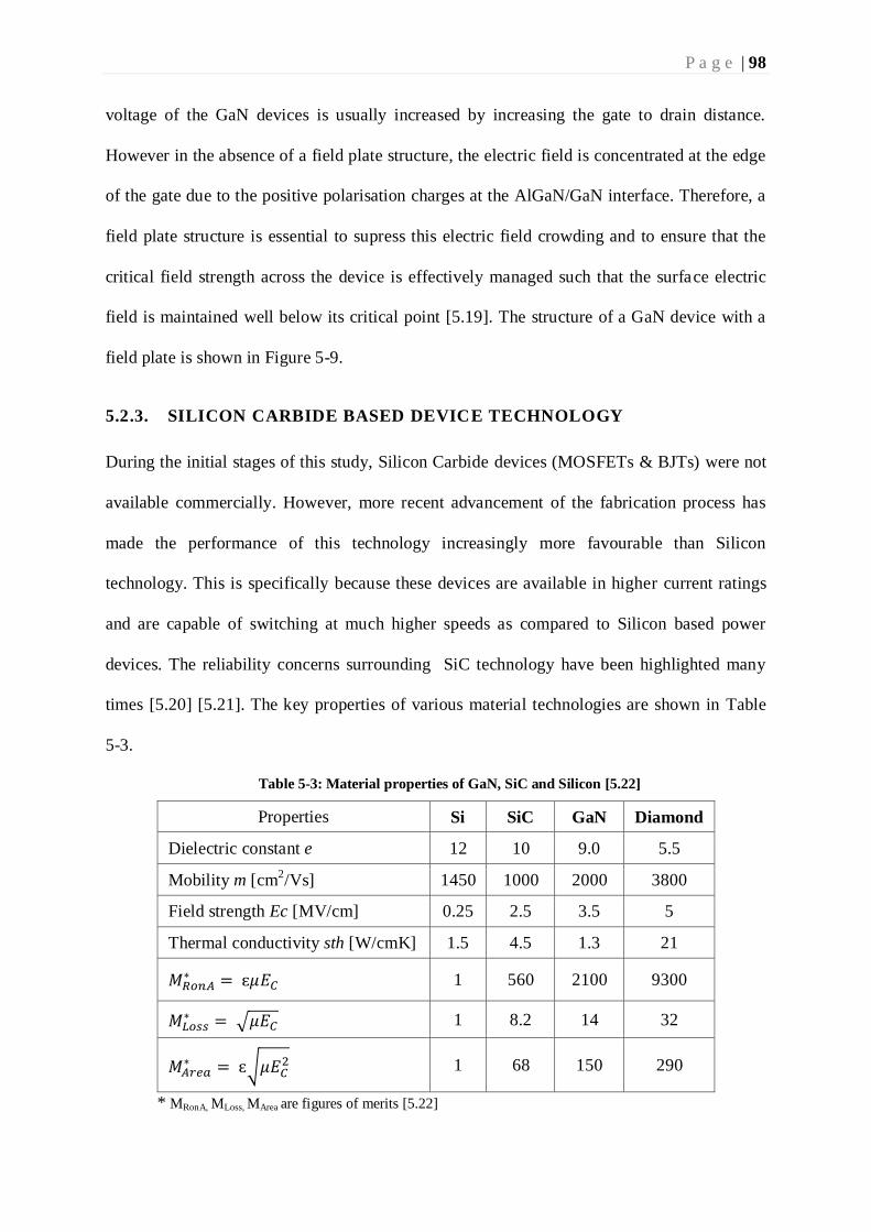
P a g e | 98
voltage of the GaN devices is usually increased by increasing the gate to drain distance.
However in the absence of a field plate structure, the electric field is concentrated at the edge
of the gate due to the positive polarisation charges at the AlGaN/GaN interface. Therefore, a
field plate structure is essential to supress this electric field crowding and to ensure that the
critical field strength across the device is effectively managed such that the surface electric
field is maintained well below its critical point [5.19]. The structure of a GaN device with a
field plate is shown in Figure 5-9.
5.2.3. SILICON CARBIDE BASED DEVICE TECHNOLOGY
During the initial stages of this study, Silicon Carbide devices (MOSFETs & BJTs) were not
available commercially. However, more recent advancement of the fabrication process has
made the performance of this technology increasingly more favourable than Silicon
technology. This is specifically because these devices are available in higher current ratings
and are capable of switching at much higher speeds as compared to Silicon based power
devices. The reliability concerns surrounding SiC technology have been highlighted many
times [5.20] [5.21]. The key properties of various material technologies are shown in Table
5-3.
Table 5-3: Material properties of GaN, SiC and Silicon [5.22]
Properties Si SiC GaN Diamond
Dielectric constant e 12 10 9.0 5.5
Mobility m [cm2/Vs] 1450 1000 2000 3800
Field strength Ec [MV/cm] 0.25 2.5 3.5 5
Thermal conductivity sth [W/cmK] 1.5 4.5 1.3 21
𝑀𝑅𝑜𝑛𝐴∗ = ɛ𝜇𝐸𝐶 1 560 2100 9300
𝑀𝐿𝑜𝑠𝑠∗ = √𝜇𝐸𝐶 1 8.2 14 32
𝑀𝐴𝑟𝑒𝑎∗ = ɛ√𝜇𝐸𝐶
2 1 68 150 290
* MRonA, MLoss, MArea are figures of merits [5.22]

P a g e | 99
It can be clearly seen that GaN will offer much better performance in comparison to SiC, and
is likely to ultimately offer a better performance/cost ratio when both technologies achieve
some comparable level of maturity.
5.3. POWER CONVERTER TOPOLOGIES
The general functionality required of any power conversion system is to convert electrical
power from one voltage and/or frequency to another in a controlled manner as efficiently as
possible. Many different power conversion topologies exist, and depending on the application
and the requirement, a preferred topology is identified. Some topologies are specifically well
suited to different motor types and some topologies are more general in that they can be used
as a motor drive as well as for bus provision. Two-level power converters are the most
commonly used for three phase converter topologies. Indeed they are the dominant topology
in low to medium power applications (i.e. <100kW). The basic circuit arrangement of a 2-
level converter is shown in Figure 5-10.
Figure 5-10: General arrangement of 3-Phase 2-Level voltage source converter
This arrangement can be considered as comprising of three single phase half bridge legs
connected across a common DC voltage bus with each leg consisting of two series-connected

P a g e | 100
semiconductors switching devices equipped with accompanying freewheeling diodes. The
rating and nature of the duty of diodes in the freewheeling path depends on the mode of
operation. The 2-level power converter can generally be operated in two distinct modes:-
1. To function as an inverter providing a variable or fixed frequency ac voltage
waveform. In this mode, the power converter could, for example, drive a multiphase
AC electrical machine or provide a multiphase controllable AC supply from a DC
bus.
2. To function as an active or passive rectifier to provide power from the AC side to the
DC-bus.
The two-level, six-switch inverter of the type shown in Figure 5-10 is often used with some
form of pulse width modulation (PWM) controller to control the switching devices, to
synthesise the desired output at its output terminals. The switching frequency used is a trade-
off between acceptable switching losses and suitable device technology and output filtering
requirements. Most Silicon based power devices can be used in this configuration with DC
bus voltages in the low kV range, as they are available at the different voltage and current
ratings. However, commercially available GaN devices are at present only rated at modest
voltage and current levels meaning that this topology would not be viable for power
applications with bus voltages of a few hundred volts and above, e.g. 270V DC and 540V DC
aerospace networks. In such cases, a multilevel converter arrangement needs to be adopted.
Indeed, multi-level converters are likely to provide a means for the outstanding performance
of low voltage Silicon MOSFETs and high performance GaN enhanced mode devices to be
exploited at representative aerospace power bus voltages.

P a g e | 101
5.3.1. MULTILEVEL CONVERTERS
In comparison to traditional two-level converters, multi-level converters can offer benefits in
terms of improved power quality by switching a greater number of lower voltage levels. This
improvement in the fidelity of the voltage waveform is achieved without increasing the
switching frequency of the devices. Moreover, they offer scope to use lower voltage rated
devices. The various other advantages and disadvantages of the multilevel converter as
compared to a two level converter as discussed in detail in [5.23] [5.24]. A summary of the
advantages and disadvantages are given below.
Key Advantages:-
o Reduced stress on semiconductor devices: One of the key motivations for adopting
multilevel converters is to reduce the voltage stress seen by the power devices to
improve reliability.
o Improved power quality: Increasing the number of levels allows the synthesis of the
output waveform with a reduced harmonic content and, in turn, an improvement in the
power quality of the converter.
o Reduction in the common mode voltage: A number of mechanical failures in
rotating machinery, principally as a result of bearing currents, have been linked to the
common mode voltage and electromagnetic interference on two-level converters. The
use of multilevel converters can result in the reduction of the common mode voltage
and EMI filtering.
Key Disadvantages:-
o Increase in complexity of the system: Since the number of individually controlled
switches increase with the number of levels, the number of gate drive and isolated

P a g e | 102
power supplies required to power the gate drive also increases. In addition to this the
complexity in the controller also increases markedly
o Voltage balancing across levels: As the number of levels increases the voltage levels
across the capacitors need to be balanced to provide a sinusoidal output.
In the early days of solid-state power converter, many devices were interconnected in very
high power and/or high voltage applications where a single power device was not able to
cope with the application requirements. In such cases, several power devices were arranged
in series and parallel combinations to improve the voltage and current handling capabilities.
However, many problems were encountered in such converters as the devices did not have
identical switching properties and hence additional circuitry was required to ensure that the
current sharing issues were resolved and to ensure that the devices were not overly stressed.
In order to accommodate such issues, in 1975 R.H.Baker and L.H.Bannister explored a new
family of power converters mainly for high power applications [5.25]. The basic idea was to
obtain the desired sinusoidal voltage by synthesising the waveform from various levels of DC
voltage applied at the input stage of the converter. These converters are commonly known as
multilevel converters. In their most elementary form there are three types of multi-level
converters:-
Cascaded multilevel converters.
Diode clamped converters.
Flying capacitor converters.
A comparison between the basic multilevel converter topologies is presented in [5.26] [5.27]
[5.28]. A brief summary of these comparisons has been captured in the Table 5-4 below. The
comparison is predominantly within the context of medium and high voltage power
applications, where the converters were initially targeted. A detailed review of more recent

P a g e | 103
emerging topologies such as the mixed-level hybrid and asymmetric hybrid multilevel cells is
contained in [5.28].
In order to explore the benefits of using a low voltage rated Silicon devices or GaN devices
within a multi-level power converter application, a cascaded H-bridge arrangement was
considered as a starting point. This topology has fewer number of power devices as compared
to a diode clamped arrangement which, in turn, has a significant bearing on the complexity
and power loss within the power converter particularly when the number of levels is
increased. In addition, the cascaded H-bridge arrangement also allows the relatively
straightforward evaluation of power loss. General arrangements of the basic multilevel
converter topologies are shown in Figure 5-11, Figure 5-12 and Figure 5-13. The operation of
such multilevel converter is described in detail in [5.24] [5.27] [5.28] [5.29].
Table 5-4: A high level comparison of the basic multi-level converter arrangements
Cascaded H-Bridge Diode Clamped Flying Capacitor
Advantages
• Intrinsic voltage sharing.
• Redundancy incorporated.
• Circuit is modular.
• Can operate from a single
DC-bus.
• Can operate from a single DC-
bus
• No diode required to clamp the
input voltage.
Disadvantages
• Each H-Bridge needs an
isolated power supply which
leads to complex transformer
arrangement.
• Voltage balancing issues
• Not modular.
• Switching pattern is
constrained.
• Difficult to build in
redundancy.
• As number of levels increases
the capacitor size increases
• Increased component count as
compared to the other
arrangements
• Capacitors needs to be pre-
charged to required voltage.
• Switching pattern is constrained.
• As number of levels increases the
capacitor size increases.

P a g e | 104
Figure 5-11: Cascaded H-Bridge Multilevel Topology (Single phase output) [5.27]
Figure 5-12: General arrangement of a diode clamped multilevel converter (Single phase output)
[5.27]
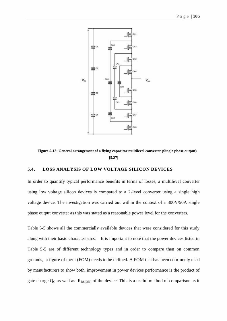
P a g e | 105
Figure 5-13: General arrangement of a flying capacitor multilevel converter (Single phase output)
[5.27]
5.4. LOSS ANALYSIS OF LOW VOLTAGE SILICON DEVICES
In order to quantify typical performance benefits in terms of losses, a multilevel converter
using low voltage silicon devices is compared to a 2-level converter using a single high
voltage device. The investigation was carried out within the context of a 300V/50A single
phase output converter as this was stated as a reasonable power level for the converters.
Table 5-5 shows all the commercially available devices that were considered for this study
along with their basic characteristics. It is important to note that the power devices listed in
Table 5-5 are of different technology types and in order to compare then on common
grounds, a figure of merit (FOM) needs to be defined. A FOM that has been commonly used
by manufacturers to show both, improvement in power devices performance is the product of
gate charge QG as well as RDS(ON) of the device. This is a useful method of comparison as it
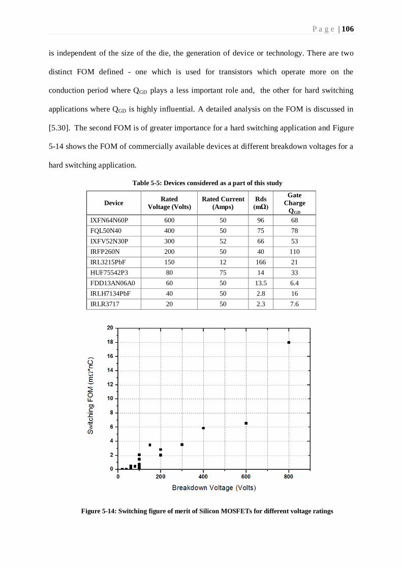
P a g e | 106
is independent of the size of the die, the generation of device or technology. There are two
distinct FOM defined - one which is used for transistors which operate more on the
conduction period where QGD plays a less important role and, the other for hard switching
applications where QGD is highly influential. A detailed analysis on the FOM is discussed in
[5.30]. The second FOM is of greater importance for a hard switching application and Figure
5-14 shows the FOM of commercially available devices at different breakdown voltages for a
hard switching application.
Table 5-5: Devices considered as a part of this study
Device Rated
Voltage (Volts)
Rated Current
(Amps)
Rds
(mΩ)
Gate
Charge
QGD
IXFN64N60P 600 50 96 68
FQL50N40 400 50 75 78
IXFV52N30P 300 52 66 53
IRFP260N 200 50 40 110
IRL3215PbF 150 12 166 21
HUF75542P3 80 75 14 33
FDD13AN06A0 60 50 13.5 6.4
IRLH7134PbF 40 50 2.8 16
IRLR3717 20 50 2.3 7.6
Figure 5-14: Switching figure of merit of Silicon MOSFETs for different voltage ratings

P a g e | 107
It can be clearly seen, from Figure 5-14 that the lower rated voltage devices can perform
much better as compared to high voltage devices in terms of this FOM. Table 5-6 shows the
total Ron of devices based on the number of levels (or H-Bridges) in the power converter.
Although the Ron of individual devices is lower for low voltage rated devices, it is important
to recognise that the effective Ron must account for the increased number of series connected
devices. Notwithstanding the need for more devices, as the device rating is reduced to 40V
the total Ron drops significantly as the drift region now contributes lesser to the on-state
performance. As will be apparent from Table 5-6, for this selection of commercial devices, a
minimum effective Ron is achieved with 40V rated devices.
Table 5-6: Ron comparison of series connected devices with number of levels
Device Rated
Voltage (Volts)
No of H-
Bridges
No-of output
levels
Effective Ron
of devices
(mΩ)
IXFN64N60P 600 1 3 190
IXFV52N30P 300 2 5 260
IRFP260N 200 3 7 240
IRL3215PbF 150 4 9 332
FDD13AN06A0 60 10 21 270
IRLH7134PbF 40 15 31 84
IRLR3717 20 30 61 138
The power losses within a converter tend to be dominated by the losses in the power
semiconductor devices. The losses within the semiconductor devices are influenced by a
number of factors. These include the conduction losses, the switching losses, forward
blocking losses, diode losses (antiparallel diode/body diode) and gate drive losses. However,
the conduction losses and the switching losses usually tend to dominate the power losses
within a MOS controlled device and hence it is reasonable to disregard the leakage losses and
other losses. The total losses in a power device can be expressed as a summation of the
conduction and switching losses as shown in equation 5.6.
𝑃𝐿𝑜𝑠𝑠𝑒𝑠 ≅ 𝑃𝐶𝑜𝑛𝑑𝑢𝑐𝑡𝑖𝑜𝑛 + 𝑃𝑆𝑤𝑖𝑡𝑐ℎ𝑖𝑛𝑔 …. (5.6)

P a g e | 108
5.4.1. EVALUATION OF CONDUCTION LOSSES
The total on-resistance for a power converter application based on the number of levels is
shown in Table 5-6. The average conduction loss within a power MOSFET in an H-Bridge
configuration for a duty cycle D can be determined by:
𝑃𝐶𝑜𝑛𝑑𝑢𝑐𝑡𝑖𝑜𝑛 = (𝑅𝐷𝑆𝑂𝑁−𝐿𝑆+𝑅𝐷𝑆𝑂𝑁−𝐻𝑆) × 𝐼𝑜𝑢𝑡(𝑟𝑚𝑠)2 × 𝐷 …. (5.7)
Where, 𝑃𝐶𝑜𝑛𝑑𝑢𝑐𝑡𝑖𝑜𝑛 = Conduction losses, 𝑅𝐷𝑆𝑂𝑁−𝐿𝑆 = On-resistance of the low side switch,
𝑅𝐷𝑆𝑂𝑁−𝐻𝑆 = On-resistance of the high side switch, 𝐼𝑜𝑢𝑡(𝑟𝑚𝑠)= RMS output current and D =
Duty cycle. The total calculated conduction losses of the converter vs the number of levels in
shown in Figure 5-15 for an rms output current of 50Amps. The total conduction losses of the
low voltage devices, especially the 31 level converters, are ~43% lower as compared to the
two-level converter thus illustrating the benefits of moving to low voltage silicon devices in
terms of conduction losses.
Figure 5-15: Variation of conduction losses in a single phase with number of levels (Silicon)

P a g e | 109
5.4.2. EVALUATION OF SWITCHING LOSSES
The time required to establish the voltage changes across the internal parasitic capacitance,
determines the switching performance of the MOSFET. This dictates that the switching
losses for similar voltage and current rated devices might vary significantly. This also means
that as the drift depth is increased, the drain to source capacitance also increases the power
dissipated during switching. The switching loss for the power devices is usually determined
by the non-zero product of the drain current and the drain source voltage as shown in
equation 5.8. The key factors that influence the switching loss of the device are:-
1. Rise and fall times of the output voltage and current,
2. Supply Voltage.
3. Output Current.
4. Frequency of operation.
Hence, the switching loss not only depends on the intrinsic properties of the switching device
but also the nature of the application. However in order to support this comparison, the
switching losses of the multilevel converter and the reference two-level converter are varied
in order to understand the impact of the application. The switching losses of the MOSFET are
usually expressed as:-
𝑃𝑆𝑤𝑖𝑡𝑐ℎ𝑖𝑛𝑔 = 1
2∗ 𝐼𝐷 ∗ 𝑉𝐷 ∗ (𝑡𝑜𝑛 + 𝑡𝑜𝑓𝑓) ∗ 𝑓 +
1
2∗ 𝐶𝑂𝑆𝑆 ∗ 𝑉𝐷
2 ∗ 𝑓 …. (5.8)
Where, 𝑃𝑆𝑤𝑖𝑡𝑐ℎ𝑖𝑛𝑔 = Switching losses, 𝐼𝐷 = Drain current, 𝑉𝐷 = Drain voltage, 𝑡𝑜𝑛= turn on
time (as per datasheet), 𝑡𝑜𝑓𝑓= turn off time (as per datasheet), 𝑓 = frequency of operation and
𝐶𝑂𝑆𝑆 = device output capacitance. The first term represents the switching loss as the area
under the ID, VD curve, while the second term accounts for the output capacitance loss. This
energy stored within the intrinsic capacitance is usually dissipated within the MOSFET
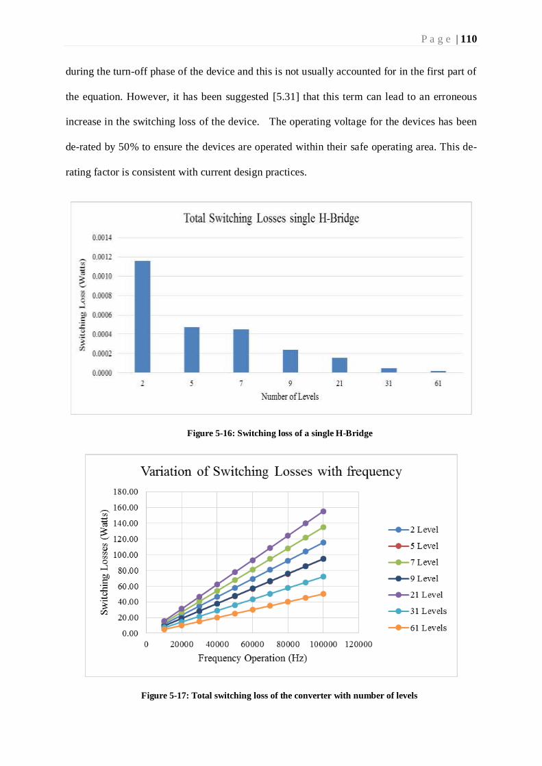
P a g e | 110
during the turn-off phase of the device and this is not usually accounted for in the first part of
the equation. However, it has been suggested [5.31] that this term can lead to an erroneous
increase in the switching loss of the device. The operating voltage for the devices has been
de-rated by 50% to ensure the devices are operated within their safe operating area. This de-
rating factor is consistent with current design practices.
Figure 5-16: Switching loss of a single H-Bridge
Figure 5-17: Total switching loss of the converter with number of levels

P a g e | 111
It is to be noted that for a similar quality of output the multilevel converter can be switched at
a lower frequency. However, this has been ignored for time being to make a comparison in
terms of the losses for similar switching frequency.
Figure 5-17 shows the resulting variation in switching losses of the power converter with the
number of levels and variation of switching frequency. It can be observed that as the
switching losses of the two-level converter seem to be more favourable as compared to a 7-
level and 21 level multilevel converters. However, it is less favourable for the other options.
This is solely due to the choice of device and its technology. The devices in the 9 -level
converter have same current rating as the GaN device hence these devices need to be
paralleled and this has been accounted in the overall calculation. It has been assumed that the
on-state resistance does not increase when these devices are paralleled. Figure 5-16 shows
the switching loss comparison for a single H-Bridge configuration. Although the switching
losses for the low voltage devices are far lower as compared to the high voltage devices, the
number of levels has a major impact overall losses.
5.4.3. TOTAL LOSSES OF LOW VOLTAGE SILICON DEVICES
This section shows the total loss of the converters with the use of low voltage silicon devices.
Figure 5-18 shows the total loss of the power converter depending on the number of levels
and with variation of switching frequency. It can be clearly seen that at a particular switching
frequency, at least for the more practical options of 5 level and 7 level, the two level Silicon
solution is more favourable in terms of losses as compared to a multilevel converter with low
voltage silicon devices. However, the 2-level converter seems to be less favourable in terms
of losses as compared to the 31-level and 61-level converters. This is due to use of fast
switching low voltage silicon devices.

P a g e | 112
Figure 5-18: Total losses in the power converter with number of levels
5.5. LOSS ANALYSIS OF GAN DEVICES
In order to compare the GaN based devices with their Silicon counterparts, a loss analysis
was performed for commercially available GaN devices. Table 5-7 shows the commercially
available GaN devices used for comparison along with their basic characteristics.
Table 5-7: Commercially available GaN devices used for comparison
Device Rated Voltage
(Volts)
Rated Current
(Amps) Rds (Ω)
Gate Charge
Qgd
EPC1010 200 12 2.50E-02 3.50E-09
EPC1011 150 12 2.50E-02 2.80E-09
EPC1001 100 25 7.00E-03 3.30E-09
EPC1005 60 25 7.00E-03 2.50E-09
EPC1015 40 33 4.00E-03 2.20E-09
In comparison to Silicon devices, the GaN devices have a much lower on-state resistance and
gate charge. This essentially means that the GaN based devices should produce lower losses
in a multilevel converter application when compared to corresponding Silicon devices. Table
5-8 shows the variation of the on-state resistance with the number of levels.

P a g e | 113
Table 5-8: Ron comparison for series connected devices with number of levels
Device
Devices
Voltage
(Volts)
No of H-
Bridges
Number of
output
Levels
Total
number of
devices
Rds(on)
mΩ
EPC1010 200 3 7 12 0.15
EPC1011 150 4 9 16 0.2
EPC1001 100 6 13 24 0.084
EPC1005 60 10 21 40 0.14
EPC1015 40 15 31 60 0.12
Similar to the silicon devices it has been assumed that the on-state resistance does not
increase when these devices are paralleled. In addition to this it has also been assumed that
these devices can be switched at the speed suggested by the manufacture and the effects of
parasitic components have been neglected.
5.5.1. EVALUATION OF CONDUCTION LOSSES
Although the operation of the GaN devices is different to those of Silicon devices, the
conduction losses of the device are still largely determined by on-resistance seen across the
device. Figure 5-19 shows the variation of conduction losses with the number of levels.
Figure 5-19: Variation of conduction losses with number of levels
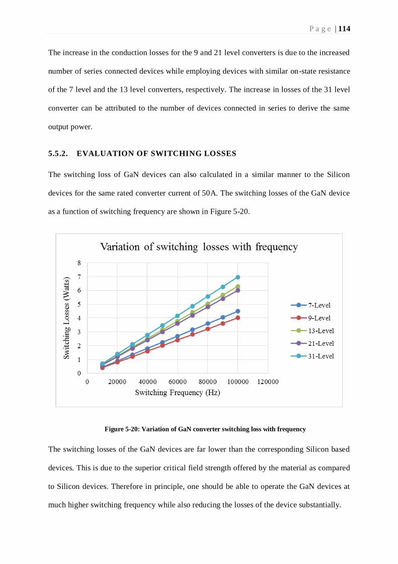
P a g e | 114
The increase in the conduction losses for the 9 and 21 level converters is due to the increased
number of series connected devices while employing devices with similar on-state resistance
of the 7 level and the 13 level converters, respectively. The increase in losses of the 31 level
converter can be attributed to the number of devices connected in series to derive the same
output power.
5.5.2. EVALUATION OF SWITCHING LOSSES
The switching loss of GaN devices can also calculated in a similar manner to the Silicon
devices for the same rated converter current of 50A. The switching losses of the GaN device
as a function of switching frequency are shown in Figure 5-20.
Figure 5-20: Variation of GaN converter switching loss with frequency
The switching losses of the GaN devices are far lower than the corresponding Silicon based
devices. This is due to the superior critical field strength offered by the material as compared
to Silicon devices. Therefore in principle, one should be able to operate the GaN devices at
much higher switching frequency while also reducing the losses of the device substantially.
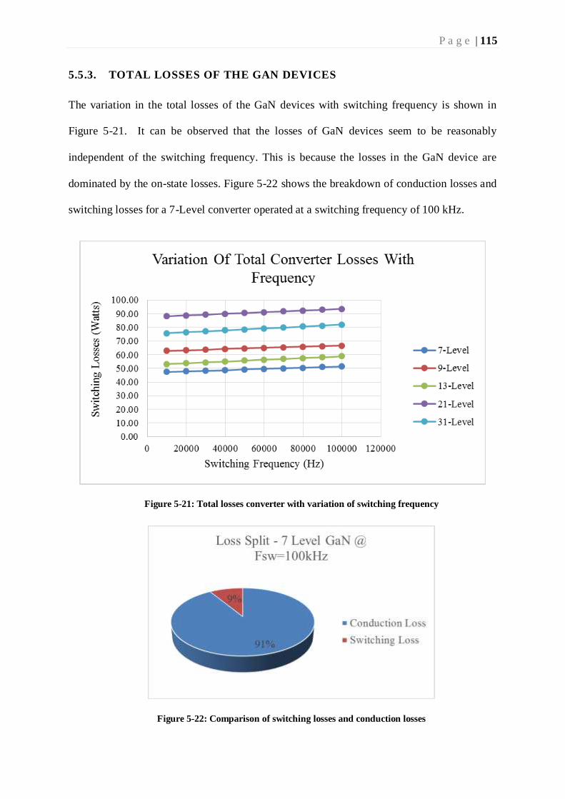
P a g e | 115
5.5.3. TOTAL LOSSES OF THE GAN DEVICES
The variation in the total losses of the GaN devices with switching frequency is shown in
Figure 5-21. It can be observed that the losses of GaN devices seem to be reasonably
independent of the switching frequency. This is because the losses in the GaN device are
dominated by the on-state losses. Figure 5-22 shows the breakdown of conduction losses and
switching losses for a 7-Level converter operated at a switching frequency of 100 kHz.
Figure 5-21: Total losses converter with variation of switching frequency
Figure 5-22: Comparison of switching losses and conduction losses

P a g e | 116
It can be clearly seen that the losses of the GaN transistor is mainly due to i ts operation in
conduction mode, and in this case it is close to 91% of the overall losses. Therefore
optimising the devices for the on-state operation would be very useful.
5.5.4. COMPARISON OF GAN AND SILICON DEVICES
Figure 5-23 shows the loss comparison of silicon devices in two-level and 31-level converters
with respect to the losses of a seven-level converter equipped with GaN devices. It can be
clearly seen that the GaN based device can offer a far superior performance in terms of losses
as compared to the Silicon based device, particularly when switching at very high
frequencies.
Figure 5-23: Comparison of GaN and Silicon devices in a multilevel converter
The total losses in a 7-Level GaN converter is 92% lower than an equivalent 2-level silicon
converter operating at 100 kHz, and 86% lower than an equivalent 31-level silicon converter
operating at 100kHz. As the GaN devices show much lower losses as compared to Silicon
devices. A multilevel converter with low voltage GaN devices is proposed. The remaining

P a g e | 117
part of this chapter experimentally compares the commercially available GaN device with an
equivalent Silicon.
5.6. EXPERIMENTAL EVALUATION OF Si AND GAN DEVICES
As demonstrated by the theoretical considerations above, a GaN device appears as a
favourable device option when compared to a Silicon MOSFET in the power range
considered. This section experimentally evaluates the performance of commercially available
GaN devices as compared to Silicon devices, so as to establish the extent to which these
theoretical properties can be achieved in a practical circuit arrangement. The GaN devices
listed previously in Table 5-8 usually come in a flip-chip package design [5.32]. The flip-chip
concept was initially developed by IBM for solid state computing systems. The
implementation of the flip-chip design in power devices is to reduce the signal inductance
and to improve the device reliability and performance.
Figure 5-24: The flip chip design used for the GaN devices
The basic principle which underpins the flip chip, is to introduce a solder bump which
replaces the solder wires used traditionally to contact the die surface. The chip is then flipped
face down onto the package carrier using a reflow process. Bump sizes ranges from 10-100
microns. Figure 5-24 shows the flip chip design for commercially available GaN devices and
Figure 5-25 shows the pad layout for the same [5.32].

P a g e | 118
Figure 5-25: The general pad layout for the EPC devices
In order to test the device performance, a PCB was developed to form the basic building
block of the power converter. The design of the PCB block is as shown in Figure 5-26.
Figure 5-26: PCB Layout for the initial testing of GaN devices
The goal was to develop a half bridge module in order to test the basic performance and the
functionality of the GaN device, and then use this as a building block to implement a
complete power converter. Q1 and Q2 form the top and bottom half devices of the phase leg
respectively. The circuit diagram for the plug-in module is contained in Appendix D.
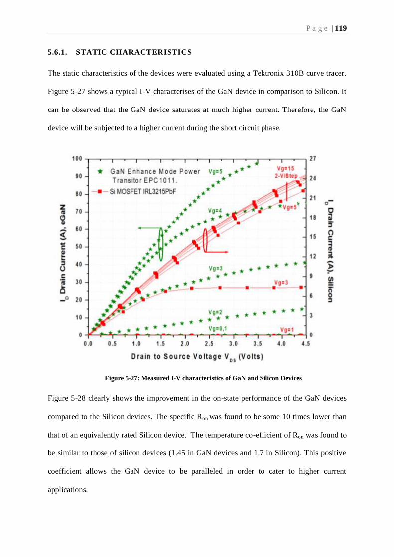
P a g e | 119
5.6.1. STATIC CHARACTERISTICS
The static characteristics of the devices were evaluated using a Tektronix 310B curve tracer.
Figure 5-27 shows a typical I-V characterises of the GaN device in comparison to Silicon. It
can be observed that the GaN device saturates at much higher current. Therefore, the GaN
device will be subjected to a higher current during the short circuit phase.
Figure 5-27: Measured I-V characteristics of GaN and Silicon Devices
Figure 5-28 clearly shows the improvement in the on-state performance of the GaN devices
compared to the Silicon devices. The specific Ron was found to be some 10 times lower than
that of an equivalently rated Silicon device. The temperature co-efficient of Ron was found to
be similar to those of silicon devices (1.45 in GaN devices and 1.7 in Silicon). This positive
coefficient allows the GaN device to be paralleled in order to cater to higher current
applications.
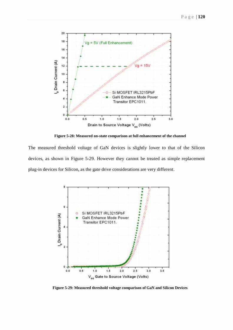
P a g e | 120
Figure 5-28: Measured on-state comparison at full enhancement of the channel
The measured threshold voltage of GaN devices is slightly lower to that of the Silicon
devices, as shown in Figure 5-29. However they cannot be treated as simple replacement
plug-in devices for Silicon, as the gate drive considerations are very different.
Figure 5-29: Measured threshold voltage comparison of GaN and Silicon Devices

P a g e | 121
It has been suggested by the GaN device manufacturer that a low inductance path should be
provided from the gate driver to the device gate pads in order to avoid undesirable turn-on of
the device during switching conditions. It is recommended that the maximum inductance at
the gate terminal be less than 2nH.
5.6.2. DYNAMIC CHARACTERISATION
The dynamic performance of the devices was measured using a clamped inductive switching
circuit similar to the one it will encounter in a hard switching application. During the initial
phase of testing, it was observed that the stray inductance associated with the setup was
prohibitive, leading to excessing oscillation in the anode output waveforms. Therefore a
snubber circuit was introduced to decouple the stray inductance associated with the test rig.
The switching results for the GaN and the Silicon devices are shown in Figure 5-30.
Figure 5-30: Experimental Turn-off switching waveforms of GaN EPC1011 and Silicon Devices
(IRL3215PbF)
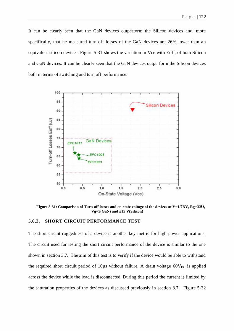
P a g e | 122
It can be clearly seen that the GaN devices outperform the Silicon devices and, more
specifically, that he measured turn-off losses of the GaN devices are 26% lower than an
equivalent silicon devices. Figure 5-31 shows the variation in Vce with Eoff, of both Silicon
and GaN devices. It can be clearly seen that the GaN devices outperform the Silicon devices
both in terms of switching and turn off performance.
Figure 5-31: Comparison of Turn-off losses and on-state voltage of the devices at V=1/2BV, Rg=22Ω,
Vg=5(GaN) and ±15 V(Silicon)
5.6.3. SHORT CIRCUIT PERFORMANCE TEST
The short circuit ruggedness of a device is another key metric for high power applications.
The circuit used for testing the short circuit performance of the device is similar to the one
shown in section 3.7. The aim of this test is to verify if the device would be able to withstand
the required short circuit period of 10µs without failure. A drain voltage 60VDC is applied
across the device while the load is disconnected. During this period the current is limited by
the saturation properties of the devices as discussed previously in section 3.7. Figure 5-32

P a g e | 123
and Figure 5-33 shows the measured short circuit performance of GaN and Silicon devices,
respectively.
Figure 5-32: Measured short Circuit Performance of GaN devices at Rg=22Ω, T=250C and Vg=5V,
VDC=60V
Figure 5-33: Short Circuit Performance of Silicon devices at Rg=22Ω, T=250C and Vg=15V,
VDC=75V

P a g e | 124
As seen in Figure 5-32, the GaN devices show a false turn-on during the end of the short
circuit period. This is due to the stray inductance associated with the gate end of the device.
Therefore, the layout of the gate driver plays a very important role in determining the
performance of the GaN device and these needs to be taken into account during the design of
the power converter.
5.7. CONCLUSION
The results presented in this chapter indicate that GaN based devices can, where appropriate
ratings exist, provide a far superior performance as compared to Silicon devices for a similar
power conversion application. The total estimated losses in the seven-Level GaN power
converter show a power loss reduction by as much as 92% and 86% as compared to the two-
level silicon converter and 31-Level silicon converter of the same rating.

P a g e | 125
5.8. REFERENCES
[5.1] H.Ohashi, "Recent Power Devices Trend," J.IEEJ, vol. 122, pp. 168-171, 2002 2002. [5.2] R. P. Zingg, "On the specific on-resistance of high-voltage and power devices,"
Electron Devices, IEEE Transactions on, vol. 51, pp. 492-499, 2004. [5.3] J. W. Kolar, U. Drofenik, J. Biela, M. L. Heldwein, H. Ertl, T. Friedli, et al., "PWM
Converter Power Density Barriers," in Power Conversion Conference - Nagoya, 2007. PCC '07, 2007, pp. P-9-P-29.
[5.4] B. Drury, Control Techniques and Drives Hand book, 2nd Edition ed.: Institution of Engineering and Technology 2009.
[5.5] J.M.Park. (2004, Novel Power Devices for Smart Power Applications. [5.6] B. J. Baliga, "Trends in power semiconductor devices," Electron Devices, IEEE
Transactions on, vol. 43, pp. 1717-1731, 1996. [5.7] B. J. Baliga, Fundamental of Power Semiconductor Devices: Springer, 2008. [5.8] G. Miller, "New semiconductor technologies challenge package and system setups,"
in Integrated Power Electronics Systems (CIPS), 2010 6th International Conference on, 2010, pp. 1-6.
[5.9] H. Haimeng and C. Xingbi, "Optimization of Specific On-Resistance of Balanced Symmetric Superjunction MOSFETs Based on a Better Approximation of Ionization Integral," Electron Devices, IEEE Transactions on, vol. 59, pp. 2742-2747, 2012.
[5.10] V. Khanna, Novel IGBT Design Concepts, Structural Innovations, and Emerging Technologies 2003.
[5.11] S. Iwamoto, K. Takahashi, H. Kuribayashi, S. Wakimoto, K. Mochizuki, and H. Nakazawa, "Above 500V class Superjunction MOSFETs fabricated by deep trench etching and epitaxial growth," in Power Semiconductor Devices and ICs, 2005. Proceedings. ISPSD '05. The 17th International Symposium on, 2005, pp. 31-34.
[5.12] J. Shuo, C. Yong, W. Deliang, Z. Baoshun, L. Kei May, and K. J. Chen, "Enhancement-mode AlGaN/GaN HEMTs on silicon substrate," Electron Devices, IEEE Transactions on, vol. 53, pp. 1474-1477, 2006.
[5.13] C. H. Chen, C. W. Yang, H. C. Chiu, and J. S. Fu, "Characteristic comparison of AlGaN/GaN enhancement-mode HEMTs with CHF<inf>3</inf> and CF<inf>4</inf> surface treatment," Journal of Vacuum Science & Technology B: Microelectronics and Nanometer Structures, vol. 30, pp. 021201-021201-6, 2012.
[5.14] W. B. Lanford, T. Tanaka, Y. Otoki, and I. Adesida, "Recessed-gate enhancement-mode GaN HEMT with high threshold voltage," Electronics Letters, vol. 41, pp. 449-450, 2005.
[5.15] Y. Uemoto, M. Hikita, H. Ueno, H. Matsuo, H. Ishida, M. Yanagihara, et al., "Gate Injection Transistor (GIT)—A Normally-Off AlGaN/GaN Power Transistor Using Conductivity Modulation," Electron Devices, IEEE Transactions on, vol. 54, pp. 3393-3399, 2007.
[5.16] X. Hu, G. Simin, J. Yang, M. A. Khan, R. Gaska, and M. S. Shur, "Enhancement mode AlGaN/GaN HFET with selectively grown pn junction gate," Electronics Letters, vol. 36, pp. 753-754, 2000.
[5.17] S. L. C. a. R. A.Beach. (2011, Fundamentals of Gallium Nitride Power Transistors. (1). [5.18] N.Zhang, "High Voltage GaN HEMTs with Low On-Resistance for Switching
Application," PhD, University of California, Santa Barbara, 2002. [5.19] A. Nakajima, M. H. Dhyani, E. M. S. Narayanan, Y. Sumida, and H. Kawai, "GaN
based Super HFETs over 700V using the polarization junction concept," in Power Semiconductor Devices and ICs (ISPSD), 2011 IEEE 23rd International Symposium on, 2011, pp. 280-283.

P a g e | 126
[5.20] T. Santini, M. Sebastien, M. Florent, L. V. Phung, and B. Allard, "Gate oxide reliability assessment of a SiC MOSFET for high temperature aeronautic applications," in ECCE Asia Downunder (ECCE Asia), 2013 IEEE, 2013, pp. 385-391.
[5.21] K. Sumi, M. Das, B. Hull, R. Sei-Hyung, J. Scofield, A. Agarwal, et al., "Gate oxide reliability of 4H-SiC MOS devices," in Reliability Physics Symposium, 2005. Proceedings. 43rd Annual. 2005 IEEE International, 2005, pp. 592-593.
[5.22] S. E. Madathil, "GaN Power Device Technologies," presented at the NMI, 2014. [5.23] M. Schweizer, I. Lizama, T. Friedli, and J. W. Kolar, "Comparison of the chip area
usage of 2-level and 3-level voltage source converter topologies," in IECON 2010 - 36th Annual Conference on IEEE Industrial Electronics Society, 2010, pp. 391-396.
[5.24] R. Teichmann and S. Bernet, "A comparison of three-level converters versus two-level converters for low-voltage drives, traction, and utility applications," Industry Applications, IEEE Transactions on, vol. 41, pp. 855-865, 2005.
[5.25] R. H. B. a. L.H.Bannister, "Electric Power Converter," U.S. Patent, 1975. [5.26] C. R. a. R. R. R. Diorge Alex Bao Zambra, "Comparison among three topologies of
multilevel inverters," 9th Brazillan Power Electronics Conference, pp. 528-533. [5.27] N. Mittal, B. Singh, S. P. Singh, R. Dixit, and D. Kumar, "Multilevel inverters: A
literature survey on topologies and control strategies," in Power, Control and Embedded Systems (ICPCES), 2012 2nd International Conference on, 2012, pp. 1-11.
[5.28] J. Rodriguez, L. Jih-Sheng, and P. Fang Zheng, "Multilevel inverters: a survey of topologies, controls, and applications," Industrial Electronics, IEEE Transactions on, vol. 49, pp. 724-738, 2002.
[5.29] L. Jih-Sheng and P. Fang Zheng, "Multilevel converters-a new breed of power converters," in Industry Applications Conference, 1995. Thirtieth IAS Annual Meeting, IAS '95., Conference Record of the 1995 IEEE, 1995, pp. 2348-2356 vol.3.
[5.30] A. Yoo, M. Chang, O. Trescases, W. Hao, and J. C. W. Ng, "FOM (Figure of Merit) Analysis for Low Voltage Power MOSFETs in DC-DC Converter," in Electron Devices and Solid-State Circuits, 2007. EDSSC 2007. IEEE Conference on, 2007, pp. 1039-1042.
[5.31] Z. J. Shen, X. Yali, C. Xu, F. Yue, and P. Kumar, "Power MOSFET Switching Loss Analysis: A New Insight," in Industry Applications Conference, 2006. 41st IAS Annual Meeting. Conference Record of the 2006 IEEE, 2006, pp. 1438-1442.
[5.32] J. C. P. a. Y. M. P. E.A. Alana Nakata, "Assembling EPC GaN Transistors," E. Corporation, Ed., ed, 2011.
P a g e | 127
CHAPTER SIX
Chapter 6
ANALYTICAL AND EXPERIMENTAL EVALUATION OF GaN BASED
DEVICES IN A MULTILEVEL CONVERTER
6.1. INTRODUCTION
In the previous chapter it was shown that low voltage Silicon devices and GaN power devices
can be used in a multilevel converter application due to their low conduction and switching
losses when compared to an appropriate higher voltage Silicon device. In this chapter, Silicon
and GaN devices are evaluated analytically in the context of a full converter in order to
validate the findings of chapter 5. The impact of using ultra low-loss power devices on other
elements of the converters such as the heat sink and passives components, are discussed. The
chapter concludes by experimentally validating the loss predictions of commercially available
GaN devices.
6.2. CONVERTER LOSS ANALYSIS
In order to establish the losses of the devices in a converter application, a circuit and an
associated loss model was developed in MATLAB-Simulink (using the simPowerSystem
toolbox). The model was developed to predict the device losses in a converter more
accurately as the voltage and current waveforms are time, temperature and load dependent.
The general block diagram of the loss model is shown in Figure 6-1. The different functional
blocks associated with the loss estimation model are described in this section.
Various methods have been discussed in literature for estimating losses of switching devices
in a converter [6.1] [6.2] [6.3] [6.4] [6.5]. Among all these methods, two distinct methods
have been used extensively to predict losses, viz. analytical loss modelling techniques and
behavioural loss modelling techniques. The analytical loss modelling technique is very useful
for determining the on-state conduction losses of the device. However, they tend to have
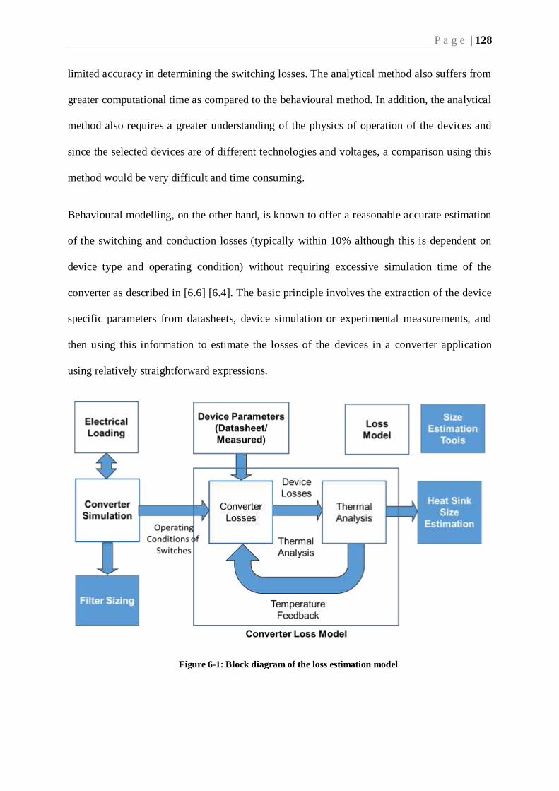
P a g e | 128
limited accuracy in determining the switching losses. The analytical method also suffers from
greater computational time as compared to the behavioural method. In addition, the analytical
method also requires a greater understanding of the physics of operation of the devices and
since the selected devices are of different technologies and voltages, a comparison using this
method would be very difficult and time consuming.
Behavioural modelling, on the other hand, is known to offer a reasonable accurate estimation
of the switching and conduction losses (typically within 10% although this is dependent on
device type and operating condition) without requiring excessive simulation time of the
converter as described in [6.6] [6.4]. The basic principle involves the extraction of the device
specific parameters from datasheets, device simulation or experimental measurements, and
then using this information to estimate the losses of the devices in a converter application
using relatively straightforward expressions.
Figure 6-1: Block diagram of the loss estimation model

P a g e | 129
This method also allows the temperature and gate drive dependency to be evaluated as they
can be included in the measurements or simulations results. This approach further allows the
simulation of various converter topologies and device technologies to be considered within a
reasonable simulation time, i.e. much shorter than analytical loss modelling techniques.
Against this background, behavioural models were preferred for estimating device losses in a
converter application. The loss model presented in this chapter comprises of the following
key blocks.
Electrical Loading Block
o This block contains the electrical load that is connected to the power converters in
order to estimate the losses in a converter. A purely resistive load was used to estimate
the losses of the devices and to understand the relative performance benefits of the
various devices selected.
Converter Simulation Block
o This block contains the basic elements of the power converter. For the purposes of
calculating current and voltage waveforms, the switching devices are simulated as
ideal switches. These waveforms then form the input for the converter loss estimation
model.
o The modulation strategy of the power converters and the reference gate signals are
also derived in this block. A phase shifted PWM modulation scheme is used to
exercise control over the current and voltage waveforms applied to the load. An open
loop control is currently considered within the simulation. The modulation scheme,
which is described in [6.7] [6.8] [6.9], is commonly used in cascaded H-bridge
converters. The modulation strategy is based around the application of modulation
signal to one half of a single H-Bridge and the phase shifted version of the signal
(phase shift=180⁰) to the other half bridge. These signals are then compared with the

P a g e | 130
triangular carriers to obtain the gate reference signals for the switching devices. The
carrier and reference signals applied to a two level converter for a carrier frequency of
10 kHz is shown in Figure 6-2. A similar method has been used to previously measure
converter losses [6.10].
Figure 6-2: Carrier and reference signals for 2 level converter using phase shifted PWM
Figure 6-3: Simulink model for single phase 2-level converter along with loss estimation block
o This block can be adapted to accommodate different devices and the number of levels
required.
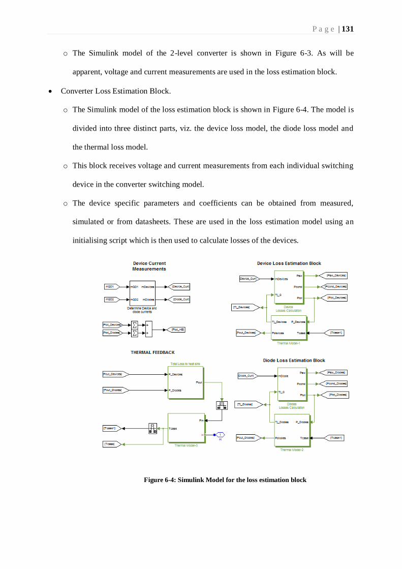
P a g e | 131
o The Simulink model of the 2-level converter is shown in Figure 6-3. As will be
apparent, voltage and current measurements are used in the loss estimation block.
Converter Loss Estimation Block.
o The Simulink model of the loss estimation block is shown in Figure 6-4. The model is
divided into three distinct parts, viz. the device loss model, the diode loss model and
the thermal loss model.
o This block receives voltage and current measurements from each individual switching
device in the converter switching model.
o The device specific parameters and coefficients can be obtained from measured,
simulated or from datasheets. These are used in the loss estimation model using an
initialising script which is then used to calculate losses of the devices.
Figure 6-4: Simulink Model for the loss estimation block
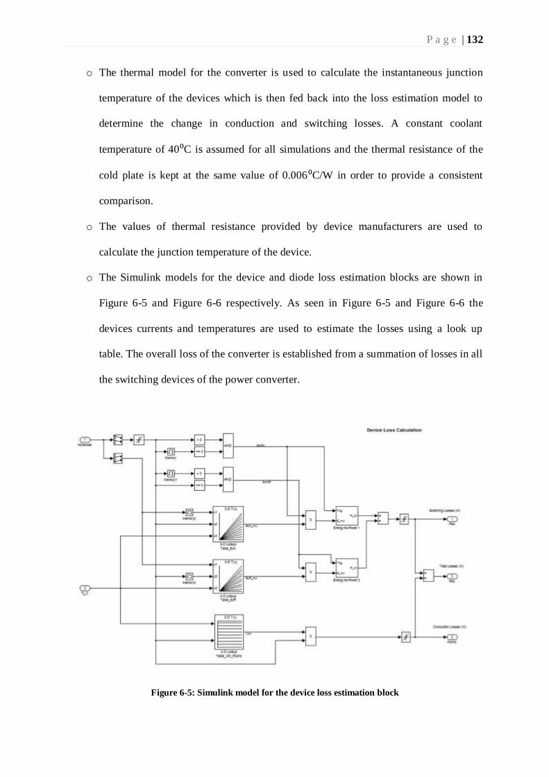
P a g e | 132
o The thermal model for the converter is used to calculate the instantaneous junction
temperature of the devices which is then fed back into the loss estimation model to
determine the change in conduction and switching losses. A constant coolant
temperature of 40⁰C is assumed for all simulations and the thermal resistance of the
cold plate is kept at the same value of 0.006⁰C/W in order to provide a consistent
comparison.
o The values of thermal resistance provided by device manufacturers are used to
calculate the junction temperature of the device.
o The Simulink models for the device and diode loss estimation blocks are shown in
Figure 6-5 and Figure 6-6 respectively. As seen in Figure 6-5 and Figure 6-6 the
devices currents and temperatures are used to estimate the losses using a look up
table. The overall loss of the converter is established from a summation of losses in all
the switching devices of the power converter.
Figure 6-5: Simulink model for the device loss estimation block
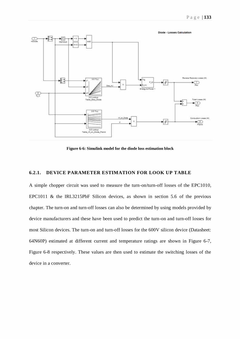
P a g e | 133
Figure 6-6: Simulink model for the diode loss estimation block
6.2.1. DEVICE PARAMETER ESTIMATION FOR LOOK UP TABLE
A simple chopper circuit was used to measure the turn-on/turn-off losses of the EPC1010,
EPC1011 & the IRL3215PbF Silicon devices, as shown in section 5.6 of the previous
chapter. The turn-on and turn-off losses can also be determined by using models provided by
device manufacturers and these have been used to predict the turn-on and turn-off losses for
most Silicon devices. The turn-on and turn-off losses for the 600V silicon device (Datasheet:
64N60P) estimated at different current and temperature ratings are shown in Figure 6-7,
Figure 6-8 respectively. These values are then used to estimate the switching losses of the
device in a converter.

P a g e | 134
Figure 6-7: Data used to estimate the turn-on losses of the converter at 2-Level Silicon based
converter at different current and temperature of operation
Figure 6-8: Data used to estimate the turn-off losses of the converter at 2-Level Silicon based
converter at different current and temperature of operation
010
2030
4050
0
50
100
1500
0.2
0.4
0.6
0.8
1
1.2
1.41.5
Operating Current (Amps)
Junction Temperature, Tj (Deg C)
Tu
rn
-on
Lo
sses,
Eoff
(m
J)

P a g e | 135
The on-state values of all the devices are estimated using the information provided in the
device datasheets. The on-state values used for the estimation of the conduction losses for the
2-level converter are shown in Figure 6-9.
Figure 6-9: Data used to measure the conduction losses of the 2-Level Silicon based converter at
different temperature and operating currents
Similar look up tables are created for all the devices in order to estimate the losses of the
devices in a converter more accurately. Similar models are used to estimate the losses of
devices in various other converter arrangements.
6.2.2. SIMULATION RESULTS
This section describes the results obtained using the models described in section 6.2. The
output waveform for the 2-level converter using standard silicon devices (i.e. devices rated at
600V) and using a 6Ω resistive load, is shown in Figure 6-10. The load resistance of the
converter was set to deliver output voltage and current of 300V/50Apeak at a fundamental
frequency of 400Hz no filtering was considered as a part of this study.

P a g e | 136
Figure 6-10: Output current and voltage waveforms of the two level converter fundamental
frequency =400Hz, Carrier frequency=10 kHz
The estimated loss for the top device in one half of the H-Bridge configuration is shown in
Figure 6-11. The loss estimations are all obtained after the converter reaches a steady state
operating condition, i.e. after the temperature reaches near steady state and the temperature
dependant coefficients in the model reach their steady-state values. The junction temperature
variation of the devices in one half of the H-Bridge circuit is shown in Figure 6-12. It can be
clearly seen that the junction temperature of the top and bottom device does not vary in a
similar manner during converter operation, which is indicative of a significant difference in
losses of the two devices.
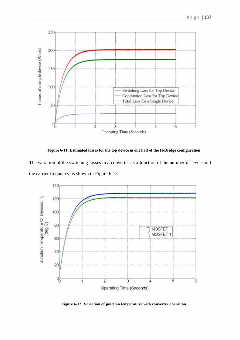
P a g e | 137
Figure 6-11: Estimated losses for the top device in one half of the H-Bridge configuration
The variation of the switching losses in a converter as a function of the number of levels and
the carrier frequency, is shown in Figure 6-13
Figure 6-12: Variation of junction temperature with converter operation

P a g e | 138
.The switching losses show a similar trend to the losses estimated in section 5.4.2 of chapter
5. This further validates the fact that a low voltage silicon device might provide lower
switching losses as compared to high voltage silicon devices.
The variation of conduction losses of the converter with the number of levels is shown in
Figure 6-14. The conductions losses also show a similar trend as compared to results
presented in chapter 5. However, the conduction losses are much higher than those indicated
in chapter 5, and this is attributed to the self-heating effect on the on-state performance of the
device. As the junction temperature of the device increases, the resistance of the device also
increases leading to more losses and therefore impacting the converter performance. It is
observed that this effect is more pronounced in high voltage devices than in low voltage
devices. This can be attributed to the temperature co-efficient of on-state resistance for the
two device ratings, i.e. (600V-2.38, 20V-1.38)
Figure 6-13: Variation of switching losses with carrier frequency

P a g e | 139
Figure 6-14: Total conduction loss of converter with number of levels
Figure 6-15: Total Losses of the converter with number of levels
Figure 6-15 shows the total losses of the various converter arrangements with a variation of
the carrier frequency.It can be clearly seen that low voltage devices silicon devices can offer
superior performance as compared to high voltage silicon devices. The trend shown in Figure

P a g e | 140
6-15 is similar to the results shown in chapter 5, further reinforcing the results presented
previously in section 5.4.3.
6.2.2.1. LOSS COMPARISON OF SILICON AND GaN BASED CONVERTERS
Figure 6-16 shows a loss comparison between GaN and Silicon devices for an operating
condition of 50A, 300V. The GaN devices show an 86% reduction in losses as compared to a
2-level silicon converter and a 51% reduction in losses as compared to a 31 level converter,
for this particular operating point. This decrease in loss in attained without increasing the
complexity of the power conversion stages and while maintaining the junction temperature of
the devices within the operating margin.
Figure 6-16: Total losses of converter GaN vs Silicon comparison (300V, 50A)
In most application the converter is expected to drive an inductive load as compared to a
resistive load. Hence, in order to make a fair comparison an RL load was also considered as a
part of this study.

P a g e | 141
Figure 6-17: Loss comparison of Silicon and GaN devices for under an RL load
Figure 6-18: Output current and voltage waveforms of the 7-level converter, Fsw=10 kHz
The selection of the inductive component was made on the basis of the power factor of the
loads and the ability to minimize the AC current ripple at the output of the converter. In most
aerospace applications it has been suggested that the system shall operate to specification

P a g e | 142
when the power factor is between 0.95 leading and 0.85 lagging [6.11] [6.12]. The inductor
value selected using this assumption is 1.2mH. Figure 6-17 shows the total losses of the
converter operating under an RL loading. The results clearly show that the GaN based
multilevel converter still outperforms the Silicon converter. The output waveforms of the 7-
level Silicon converter under the RL load is shown in Figure 6-18. It can also be seen that the
total losses of the converter have reduced this is because the on-state voltages and switching
currents are load dependent.
6.2.3. IMPACT ON PASSIVE FILTER
Figure 6-19 shows the output voltage waveforms of the 2-Level, 7-level and the 31-level
converter at a carrier frequency of 10 kHz.
Figure 6-19: Output voltage of a 2-level, 7-level and 31-Level converter at a switching frequency of 10
kHz and 300V/50Amps
It can be clearly seen that as the number of levels are increased, the output voltage of the
converter has markedly fewer harmonics when all converters are switched at the same

P a g e | 143
frequency. Hence, the extent of filtering required for a higher level converter would be much
lower in weight and volume as compared to a two level converter although it is also worth
noting that the increased number of levels could be exploited to reduce the switching
frequency and losses for the same level of harmonic distortion. In practice, some trade-off
between these two positions is adopted.
6.2.3.1. HARMONIC ANALYSIS OF THE OUTPUT VOLTAGE
In many power conversion applications, especially those concerning aerospace, it is highly
desirable that the output waveform has low harmonic distortion in order to avoid signal
interference with other electrical equipment and also to comply with appropriate standards.
Many applications specify a THD content of less than 5% [6.11] in order allow compliance
with network requirements, although in practice standards are rather more complex in setting
different constrains in different frequency ranges. Equation 5.1 describes the basic formula
used to define the output voltage of the converter. Using Fourier analysis method it is
possible to determine the total harmonic distortion of the power converter based on the
number of levels.
𝑉𝑚(𝜃) = ∑4
𝑛𝜋(𝑉1 cos(𝑛𝜃1) ± 𝑉2 cos(n𝜃2)
∞
𝑛=1,3,5
± 𝑉3 cos(n𝜃3)± ⋯ ± 𝑉𝑠 cos(n𝜃𝑠)) sin(𝑛𝜔𝑡) … . (6.1)
Where total harmonic distortion (THD) can be defined the root mean square (RMS) value of
the total harmonics of the signal, divided by the RMS value of this fundamental signal.
Figure 6-20 shows a comparison of a total harmonic distortion with a number of levels, for a
300V/50A power conversion application. It can be seen that a 31-level converter eliminates
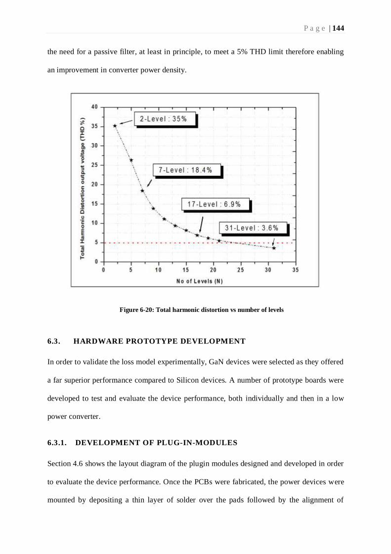
P a g e | 144
the need for a passive filter, at least in principle, to meet a 5% THD limit therefore enabling
an improvement in converter power density.
Figure 6-20: Total harmonic distortion vs number of levels
6.3. HARDWARE PROTOTYPE DEVELOPMENT
In order to validate the loss model experimentally, GaN devices were selected as they offered
a far superior performance compared to Silicon devices. A number of prototype boards were
developed to test and evaluate the device performance, both individually and then in a low
power converter.
6.3.1. DEVELOPMENT OF PLUG-IN-MODULES
Section 4.6 shows the layout diagram of the plugin modules designed and developed in order
to evaluate the device performance. Once the PCBs were fabricated, the power devices were
mounted by depositing a thin layer of solder over the pads followed by the alignment of

P a g e | 145
devices on the solder pads and a reflow process. Figure 6-21 shows the deposition of solder
on the PCB and Figure 6-22 shows the device after the reflow process. The temperature
profile for the reflow process is defined in [6.5].
Figure 6-21: Deposition of solder on the PCB boards
Figure 6-22: Picture of device post assembly
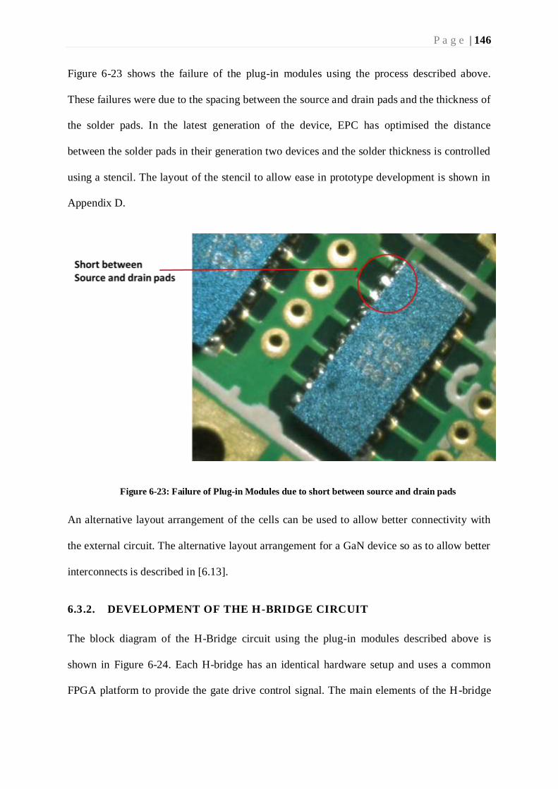
P a g e | 146
Figure 6-23 shows the failure of the plug-in modules using the process described above.
These failures were due to the spacing between the source and drain pads and the thickness of
the solder pads. In the latest generation of the device, EPC has optimised the distance
between the solder pads in their generation two devices and the solder thickness is controlled
using a stencil. The layout of the stencil to allow ease in prototype development is shown in
Appendix D.
Figure 6-23: Failure of Plug-in Modules due to short between source and drain pads
An alternative layout arrangement of the cells can be used to allow better connectivity with
the external circuit. The alternative layout arrangement for a GaN device so as to allow better
interconnects is described in [6.13].
6.3.2. DEVELOPMENT OF THE H-BRIDGE CIRCUIT
The block diagram of the H-Bridge circuit using the plug-in modules described above is
shown in Figure 6-24. Each H-bridge has an identical hardware setup and uses a common
FPGA platform to provide the gate drive control signal. The main elements of the H-bridge

P a g e | 147
circuit are: Switching devices: Manufacturer part number EPC 1010 (Generation 1 devices)
and EPC 1011 (Generation 1 devices). These GaN devices are rated at 200V-12A and 150-
12A, respectively. A series of H-bridge circuits will be required to provide the 300V output.
However in order to determine the losses, a single device or H-bridge arrangement would
suffice.
Figure 6-24: Block diagram of the H-Bridge Circuit
Gate Drivers: The EL7158 Gate driver IC is used to generate the high and low side-
gate drive signals independently. The dead time is configured in the FPGA code and
sufficient dead time is provided in order to avoid shoot through of the devices,
typically <10ns as recommended by the device manufacturer.
Optical Isolator: An optical isolator is used to isolate the logic signals from the power
stage (HCPL0600).
Voltage Regulator: A MIC5377 voltage regulator is used to ensure the gate drive
supply signals do not exceed 0-5V in order to operate the devices within their
operating margin.

P a g e | 148
DC-DC Converter: A LME120 DC-DC converter is used to provide isolated power
stages for the gate driver and other ancillary components.
The drive circuitry for a single device is shown in Figure 6-25 and the layout diagram for the
individual H-Bridges is shown in Appendix D (D-11) The high voltage/power stage is
separated from the low stage or logic stage as shown in the figure.
Figure 6-25: Drive circuit for the top device in one half of the H-bridge
The completed H-bridge circuit in a 5-level multilevel converter arrangement is shown in
Figure 6-26. Each isolated H-bridge circuit is powered using an isolated DC-Power supply,
which acts as the DC-Link for the H-bridge circuit.
6.3.3. DEVELOPMENT OF THE 5-LEVEL CONVERTER CIRCUIT
Figure 6-26 shows the completed H-Bridge circuit modules in a 5-level converter
arrangement. The SPARTAN 3E-500 FG320 FPGA board is used to provide control signals
for the gate drivers based on the modulation strategy. The specification of this demonstration
board is described in [6.12].

P a g e | 149
Figure 6-26: Completed H-Bridge Circuit in a 5-phase converter arrangement
The key features of the demonstration board are:
1. 16MB of Micron PSDRAN and 16 MB of Intel Strata Flash ROM.
2. 50MHz Oscillator plus socket for second oscillator.
3. 50 FPGA I/O routed to expansion connectors (one high speed Hirose FX2 connector
and four 6-pin headers).
4. 8 LEDs, 4-digit 7-Seg display, 4 buttons, 8 slide switches.
5. 12-Pin PMOD connectors allow addition of features like motor control, A/D and D/A
Conversion.
6. Can be powered by bench top power supplies via a PMOD connectors.
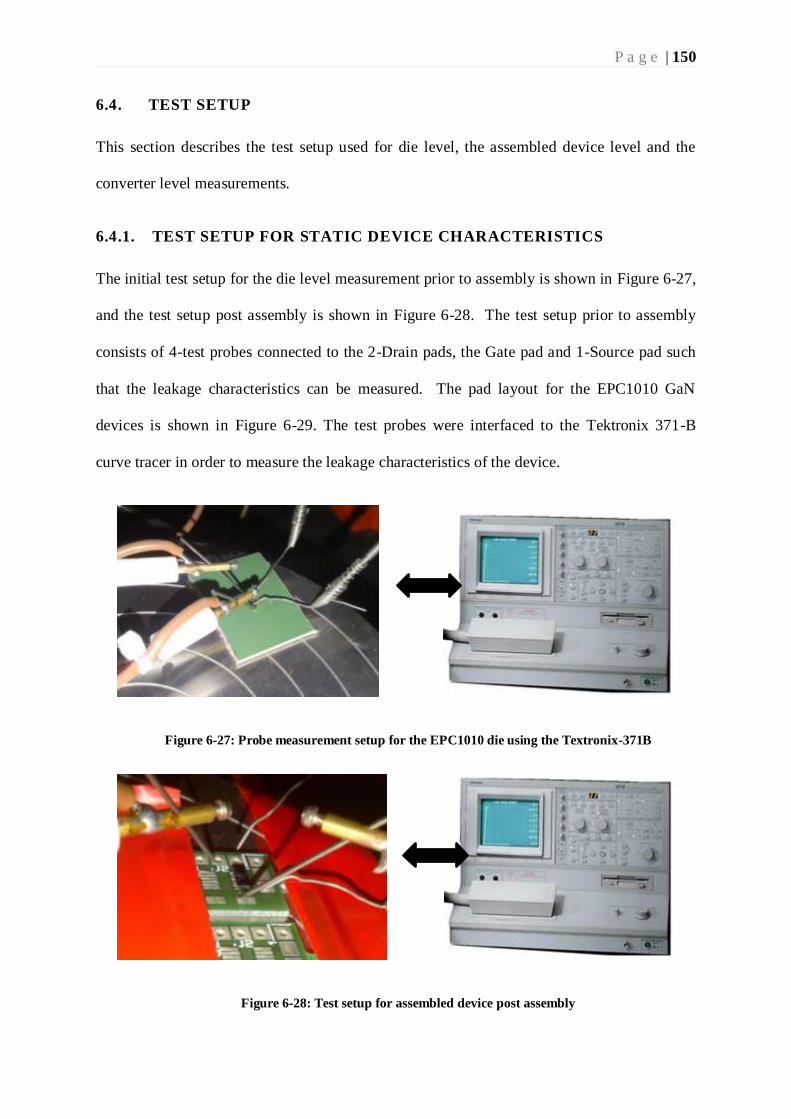
P a g e | 150
6.4. TEST SETUP
This section describes the test setup used for die level, the assembled device level and the
converter level measurements.
6.4.1. TEST SETUP FOR STATIC DEVICE CHARACTERISTICS
The initial test setup for the die level measurement prior to assembly is shown in Figure 6-27,
and the test setup post assembly is shown in Figure 6-28. The test setup prior to assembly
consists of 4-test probes connected to the 2-Drain pads, the Gate pad and 1-Source pad such
that the leakage characteristics can be measured. The pad layout for the EPC1010 GaN
devices is shown in Figure 6-29. The test probes were interfaced to the Tektronix 371-B
curve tracer in order to measure the leakage characteristics of the device.
Figure 6-27: Probe measurement setup for the EPC1010 die using the Textronix-371B
Figure 6-28: Test setup for assembled device post assembly
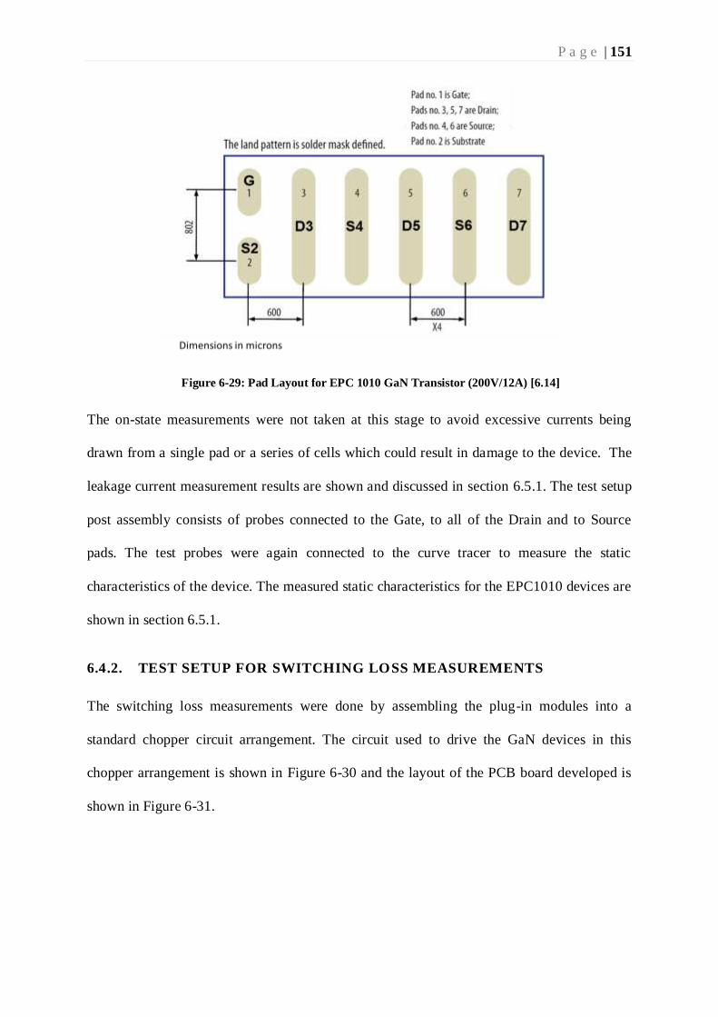
P a g e | 151
Figure 6-29: Pad Layout for EPC 1010 GaN Transistor (200V/12A) [6.14]
The on-state measurements were not taken at this stage to avoid excessive currents being
drawn from a single pad or a series of cells which could result in damage to the device. The
leakage current measurement results are shown and discussed in section 6.5.1. The test setup
post assembly consists of probes connected to the Gate, to all of the Drain and to Source
pads. The test probes were again connected to the curve tracer to measure the static
characteristics of the device. The measured static characteristics for the EPC1010 devices are
shown in section 6.5.1.
6.4.2. TEST SETUP FOR SWITCHING LOSS MEASUREMENTS
The switching loss measurements were done by assembling the plug-in modules into a
standard chopper circuit arrangement. The circuit used to drive the GaN devices in this
chopper arrangement is shown in Figure 6-30 and the layout of the PCB board developed is
shown in Figure 6-31.
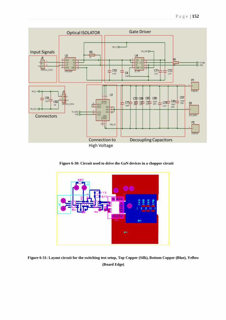
P a g e | 152
Figure 6-30: Circuit used to drive the GaN devices in a chopper circuit
Figure 6-31: Layout circuit for the switching test setup, Top Copper (Silk), Bottom Copper (Blue), Yellow
(Board Edge)
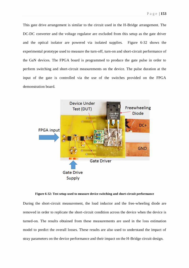
P a g e | 153
This gate drive arrangement is similar to the circuit used in the H-Bridge arrangement. The
DC-DC converter and the voltage regulator are excluded from this setup as the gate driver
and the optical isolator are powered via isolated supplies. Figure 6-32 shows the
experimental prototype used to measure the turn-off, turn-on and short-circuit performance of
the GaN devices. The FPGA board is programmed to produce the gate pulse in order to
perform switching and short-circuit measurements on the device. The pulse duration at the
input of the gate is controlled via the use of the switches provided on the FPGA
demonstration board.
Figure 6-32: Test setup used to measure device switching and short-circuit performance
During the short-circuit measurement, the load inductor and the free-wheeling diode are
removed in order to replicate the short-circuit condition across the device when the device is
turned-on. The results obtained from these measurements are used in the loss estimation
model to predict the overall losses. These results are also used to understand the impact of
stray parameters on the device performance and their impact on the H-Bridge circuit design.

P a g e | 154
6.4.3. TEST SETUP FOR CONVERTER LOSS MEASUREMENTS
The test setup used to measure the losses of a 5-level converter arrangement is shown in
Figure 6-33. This test setup consists of the following components:
Two isolated power supplies to provide power to the isolated H-Bridges.
Thermocouples which are mounted on the top of the devices in order to monitor case
temperatures.
The resistive load back used load the converter. The measured resistance and of the
load banks is provided in Table 6-1. The load bank consists of 7 resistors in parallel.
The switches located on top of the load banks are used to select the channels used for
testing.
Table 6-1: Measured resistance of the Load Bank
Measured Resistance (Ω) Measured Stray
inductance
Resistor 1 859 120 µH
Resistor 2 455.7 31.5 µH
Resistor 3 203.4 24.1 µH
Resistor 4 124.4 12.7 µH
Resistor 5 62.5 11.1 µH
Resistor 6 34.4 10.8 µH
Resistor 7 14.4 3.3 µH
Oscilloscope which is used monitor the gate voltages and input/output voltages and
currents.
A low voltage power supply which is used to power the gate drivers and other
components.
As the devices have a very small foot print and are very fragile, it was very difficult to
mount a heat sink without damaging the device. The circuit considered within this chapter
is operated at very low power levels in order to keep the case temperature within the

P a g e | 155
operating margin. An optimised layout could be developed to force air-cooling of the
devices, thus facilitating higher power operation.
Figure 6-33: Test setup for the 5-Level converter
6.5. EXPERIMENTAL RESULTS
6.5.1. FORWARD BREAKDOWN VOLTAGE MEASUREMENTS
In order to understand whether the dies are able to withstand the breakdown voltages, the
drain pads were subjected to a series of high voltages (i.e. between 0V and less than the
breakdown voltage of the device) with the source and gate pads grounded. Due to limitations
on the number probe points available, alternate source and drain pads of the device were used
during the measurements. Figure 6-34 shows the breakdown characteristics of the devices as
a function of anode voltage. It can be clearly seen that the GaN devices have a significantly
higher leakage current as compared to Silicon devices. This, in turn, will result in the GaN
devices having higher blocking losses compared to Silicon devices. However, as the leakage
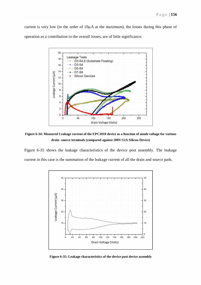
P a g e | 156
current is very low (in the order of 10A at the maximum), the losses during this phase of
operation as a contribution to the overall losses, are of little significance.
Figure 6-34: Measured Leakage current of the EPC1010 device as a function of anode voltage for various
drain -source terminals (compared against 200V/12A Silicon Device)
Figure 6-35 shows the leakage characteristics of the device post assembly. The leakage
current in this case is the summation of the leakage current of all the drain and source pads.
Figure 6-35: Leakage characteristics of the device post device assembly

P a g e | 157
This essentially highlights that the drain and source pads might not be connected internally
and hence require a good interface to the PCB boards to ensure good use of device active
area. It is also observed that the performance of the device under reverse blocking condition
is within the bounds defined by the manufacturer datasheet. The equipment setup used to
measure the leakage properties of the device was described previously in 6.4.1.
The hysteresis observed in Figure 6-34 and Figure 6-35 is due to the loop compensation of
the curve tracer. The loop compensation is used to compensate for the stray capacitance
which might occur within 371B as given in [6.15]. It is also observed that these GaN devices
do not have avalanche capability.
6.5.2. STATIC MEASUREMENTS
The measured static characterises of the EPC1011 (150V-12A) GaN devices is shown in
section 5.6.1. The measured static characteristics for single EPC 1010 devices and 2 devices
connected in parallel are shown in Figure 6-36. As seen in the figure, the on-state voltage for
2-devices connected in parallel is higher than the single device. The on-state voltage of the
EPC1010 device with 2-devices connected in parallel is ~0.1 V higher compared to the single
device, a factor that will impact the conduction losses of the converter. The performance of
body diodes with variation of anode voltage is shown in Figure 6-37. It can be clearly seen
that GaN devices have a significantly lower performance as compared to Silicon devices in
terms of their body diode. The on-state resistance (Ron) of the body diodes is some 5 times
higher than that in the Silicon devices, a difference which arises from the fact that the
intrinsic properties of the GaN device are very different to those of Silicon devices.

P a g e | 158
Figure 6-36: Typical I-V characteristics of EPC1010 GaN Devices
Figure 6-37: Typical forward characteristics of the body diode with drain-source current
0.0 0.5 1.0 1.5 2.0 2.5 3.0 3.5
0.0
0.1
0.2
0.3
0.4
0.5
0.6
0.7
0.8
0.9
1.0
Si MOSFET IRL3215P bF
eGaN EPC1010 - 200V
Sou
rce
to
Dra
in c
urr
en
t I s
d (
Am
ps)
Source to Drain Voltage Vsd
(Volts)
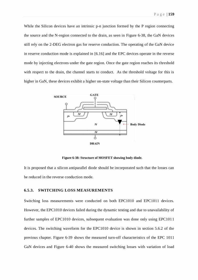
P a g e | 159
While the Silicon devices have an intrinsic p-n junction formed by the P region connecting
the source and the N-region connected to the drain, as seen in Figure 6-38, the GaN devices
still rely on the 2-DEG electron gas for reserve conduction. The operating of the GaN device
in reserve conduction mode is explained in [6.16] and the EPC devices operate in the reverse
mode by injecting electrons under the gate region. Once the gate region reaches its threshold
with respect to the drain, the channel starts to conduct. As the threshold voltage for this is
higher in GaN, these devices exhibit a higher on-state voltage than their Silicon counterparts.
Figure 6-38: Structure of MOSFET showing body diode.
It is proposed that a silicon antiparallel diode should be incorporated such that the losses can
be reduced in the reverse conduction mode.
6.5.3. SWITCHING LOSS MEASUREMENTS
Switching loss measurements were conducted on both EPC1010 and EPC1011 devices.
However, the EPC1010 devices failed during the dynamic testing and due to unavailability of
further samples of EPC1010 devices, subsequent evaluation was done only using EPC1011
devices. The switching waveform for the EPC1010 device is shown in section 5.6.2 of the
previous chapter. Figure 6-39 shows the measured turn-off characteristics of the EPC 1011
GaN devices and Figure 6-40 shows the measured switching losses with variation of load
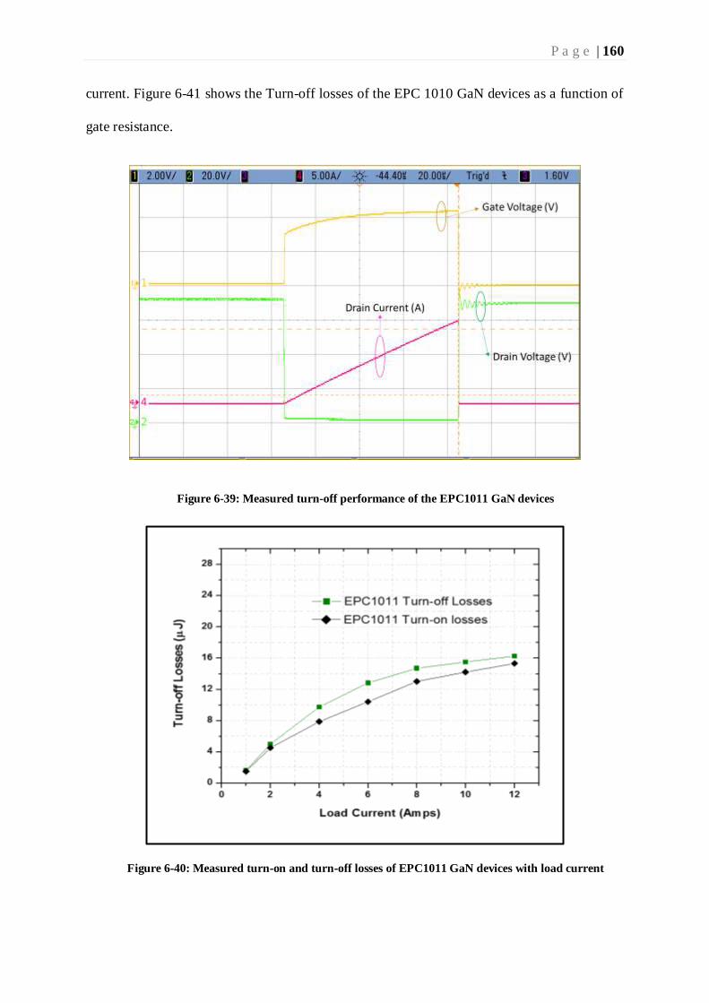
P a g e | 160
current. Figure 6-41 shows the Turn-off losses of the EPC 1010 GaN devices as a function of
gate resistance.
Figure 6-39: Measured turn-off performance of the EPC1011 GaN devices
Figure 6-40: Measured turn-on and turn-off losses of EPC1011 GaN devices with load current
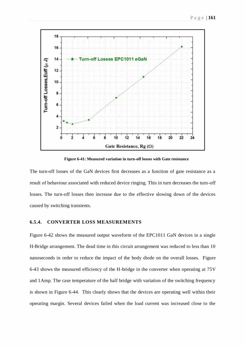
P a g e | 161
Figure 6-41: Measured variation in turn-off losses with Gate resistance
The turn-off losses of the GaN devices first decreases as a function of gate resistance as a
result of behaviour associated with reduced device ringing. This in turn decreases the turn-off
losses. The turn-off losses then increase due to the effective slowing down of the devices
caused by switching transients.
6.5.4. CONVERTER LOSS MEASUREMENTS
Figure 6-42 shows the measured output waveform of the EPC1011 GaN devices in a single
H-Bridge arrangement. The dead time in this circuit arrangement was reduced to less than 10
nanoseconds in order to reduce the impact of the body diode on the overall losses. Figure
6-43 shows the measured efficiency of the H-bridge in the converter when operating at 75V
and 1Amp. The case temperature of the half bridge with variation of the switching frequency
is shown in Figure 6-44. This clearly shows that the devices are operating well within their
operating margin. Several devices failed when the load current was increased close to the

P a g e | 162
rated current and since generation 1 samples were no longer available, it was not possible to
measure any further losses.
Figure 6-42: Measured output voltage and current waveforms of a single H-Bridge using EPC1011
devices (Switching frequency=10 kHz, DC link 60V)
Figure 6-43: Measured efficiency of the H-Bridge circuit using EPC1011 devices (Vout=60V,
Iout=1A)
0 10 20 30 40 50 60 70 80
86
88
90
92
94
96
98
100
Eff
icie
ncy (),
%
Switching Frequency (kHz)
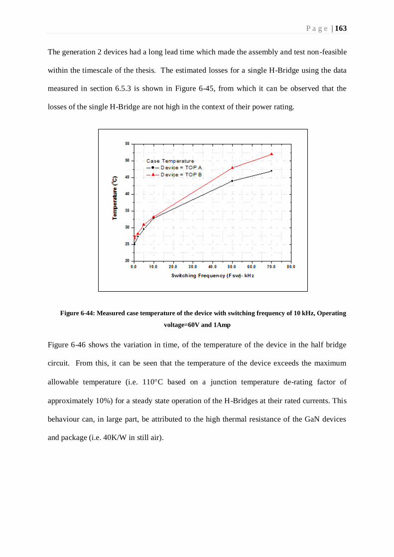
P a g e | 163
The generation 2 devices had a long lead time which made the assembly and test non-feasible
within the timescale of the thesis. The estimated losses for a single H-Bridge using the data
measured in section 6.5.3 is shown in Figure 6-45, from which it can be observed that the
losses of the single H-Bridge are not high in the context of their power rating.
Figure 6-44: Measured case temperature of the device with switching frequency of 10 kHz, Operating
voltage=60V and 1Amp
Figure 6-46 shows the variation in time, of the temperature of the device in the half bridge
circuit. From this, it can be seen that the temperature of the device exceeds the maximum
allowable temperature (i.e. 110C based on a junction temperature de-rating factor of
approximately 10%) for a steady state operation of the H-Bridges at their rated currents. This
behaviour can, in large part, be attributed to the high thermal resistance of the GaN devices
and package (i.e. 40K/W in still air).
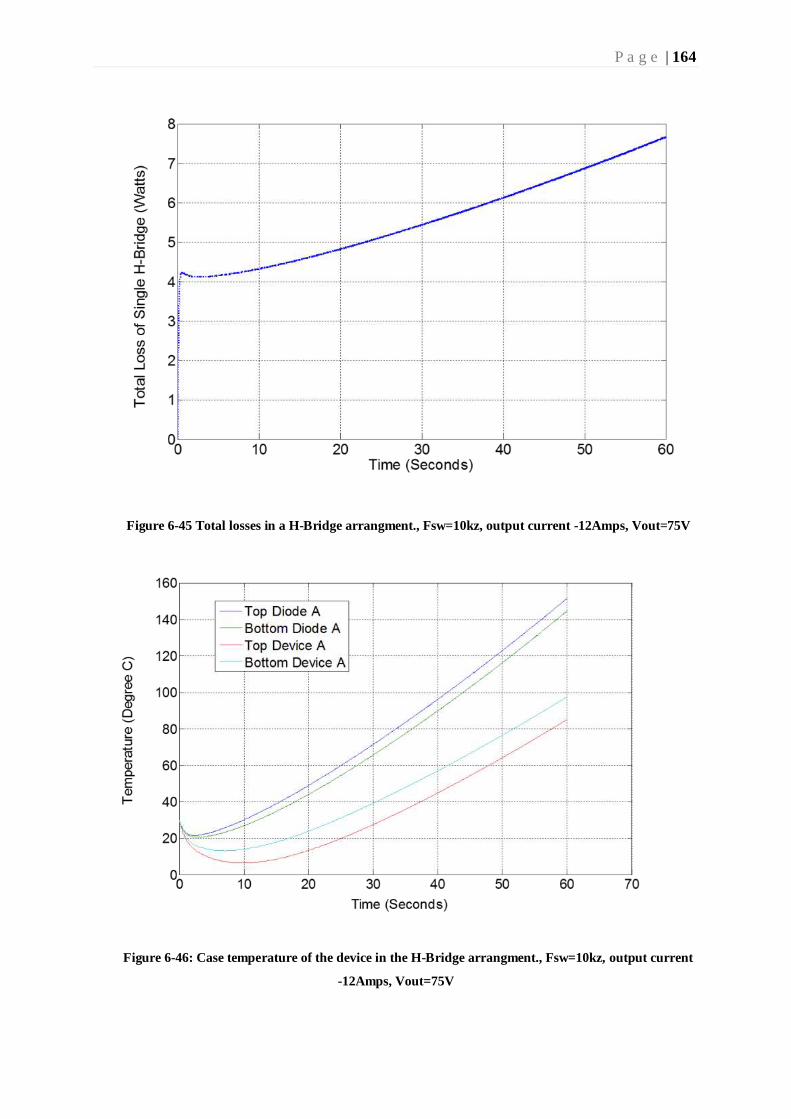
P a g e | 164
Figure 6-45 Total losses in a H-Bridge arrangment., Fsw=10kz, output current -12Amps, Vout=75V
Figure 6-46: Case temperature of the device in the H-Bridge arrangment., Fsw=10kz, output current
-12Amps, Vout=75V

P a g e | 165
6.6. CONCLUSION
In order to verify the results presented in chapter 5 a simulation bench was created to estimate
the losses of the converter. The switching losses and on-state performance of the EPC1011
and EPC1010 devices were experimental obtained at different currents and temperatures.
These were then fed into the model to estimate the losses in the converter application.
The results presented here clearly support the results presented in chapter 5. The simulation
results clearly show that the 7-level GaN multilevel converter can offer up to 86% reduction
in losses as compared to an equivalent 2-level converter in Silicon. Figure 6-16 also shows
that the 31-level converter provides much lower losses as compared to the 2-level converter
this is due to the use of low loss low voltage devices. However, the reduction in losses is
offset by the reliability and complexity of the converter due to increased number of levels
making the 31-level solution less feasible.
As the GaN devices offered a far more superior performance as compared to Silicon devices,
particularly in terms of conduction and switching losses, work was undertaken to evaluate
these devices first individually, then in an H-bridge arrangement and then subsequently build
a 7-level converter to provide a proof of concept. Various challenges were encountered
during these stages. These included availability of devices, assembly of the devices, reduction
of stray inductance in the circuit, paralleling of devices, and assembly of devices on a heat
sink to provide sufficient cooling. It was noted that although these devices offer a far superior
performance they cannot be treated as like for like replacement of silicon devices. As the
packaging solution provided makes them inherently fragile to use. In addition to this the
thermal conductivity of the GaN devices is lower when compared to Silicon. Therefore the
surface area of the PCB used to mount the devices also had to be optimised to provide
adequate cooling. Without the use of adequate thermal management solution the GaN devices

P a g e | 166
could not be operated at their full rated power. This meant that the losses could not be
validated at full power and was only validated at low current levels.
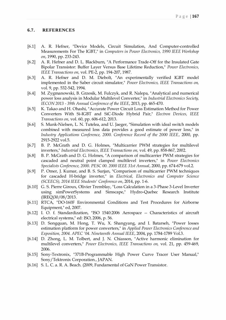
P a g e | 167
6.7. REFERENCES
[6.1] A. R. Hefner, "Device Models, Circuit Simulation, And Computer-controlled Measurements For The IGBT," in Computers in Power Electronics, 1990 IEEE Workshop on, 1990, pp. 233-243.
[6.2] A. R. Hefner and D. L. Blackburn, "A Performance Trade-Off for the Insulated Gate Bipolar Transistor: Buffer Layer Versus Base Lifetime Reduction," Power Electronics, IEEE Transactions on, vol. PE-2, pp. 194-207, 1987.
[6.3] A. R. Hefner and D. M. Diebolt, "An experimentally verified IGBT model implemented in the Saber circuit simulator," Power Electronics, IEEE Transactions on,
vol. 9, pp. 532-542, 1994. [6.4] M. Zygmanowski, B. Grzesik, M. Fulczyk, and R. Nalepa, "Analytical and numerical
power loss analysis in Modular Multilevel Converter," in Industrial Electronics Society, IECON 2013 - 39th Annual Conference of the IEEE, 2013, pp. 465-470.
[6.5] K. Takao and H. Ohashi, "Accurate Power Circuit Loss Estimation Method for Power Converters With Si-IGBT and SiC-Diode Hybrid Pair," Electron Devices, IEEE Transactions on, vol. 60, pp. 606-612, 2013.
[6.6] S. Munk-Nielsen, L. N. Tutelea, and U. Jaeger, "Simulation with ideal switch models combined with measured loss data provides a good estimate of power loss," in Industry Applications Conference, 2000. Conference Record of the 2000 IEEE, 2000, pp. 2915-2922 vol.5.
[6.7] B. P. McGrath and D. G. Holmes, "Multicarrier PWM strategies for multilevel inverters," Industrial Electronics, IEEE Transactions on, vol. 49, pp. 858-867, 2002.
[6.8] B. P. McGrath and D. G. Holmes, "A comparison of multicarrier PWM strategies for cascaded and neutral point clamped multilevel inverters," in Power Electronics Specialists Conference, 2000. PESC 00. 2000 IEEE 31st Annual, 2000, pp. 674-679 vol.2.
[6.9] P. Omer, J. Kumar, and B. S. Surjan, "Comparison of multicarrier PWM techniques for cascaded H-bridge inverter," in Electrical, Electronics and Computer Science (SCEECS), 2014 IEEE Students' Conference on, 2014, pp. 1-6.
[6.10] G. S. Pierre Giroux, Olivier Tremblay, "Loss Calculation in a 3-Phase 3-Level Inverter using simPowerSystems and Simscape," Hydro-Quebec Research Institute (IREQ)30/08/2013.
[6.11] RTCA, "DO-160F Environmental Conditions and Test Procedures for Airborne Equipment," ed, 2007.
[6.12] I. O. f. Standardization, "ISO 1540:2006 Aerospace -- Characteristics of aircraft electrical systems," ed: ISO, 2006, p. 56.
[6.13] D. Songquan, M. Hong, T. Wu, X. Shangyang, and I. Batarseh, "Power losses estimation platform for power converters," in Applied Power Electronics Conference and Exposition, 2004. APEC '04. Nineteenth Annual IEEE, 2004, pp. 1784-1789 Vol.3.
[6.14] D. Zhong, L. M. Tolbert, and J. N. Chiasson, "Active harmonic elimination for multilevel converters," Power Electronics, IEEE Transactions on, vol. 21, pp. 459-469, 2006.
[6.15] Sony-Textronix, "371B-Programmable High Power Curve Tracer User Manual," Sony/Tektronix Corporation., JAPAN.
[6.16] S. L. C. a. R. A. Beach. (2009, Fundamental of GaN Power Transistor.

P a g e | 168
CHAPTER SEVEN
Chapter 7
CONCLUSION AND FUTURE WORK
7.1. CONCLUSION
In the research reported in this thesis, numerous design aspects that might affect device and
converter performance were investigated, discussed and evaluated in detail. The various
methods of optimising the device losses and the converter loss performance have been
discussed and experimentally evaluated starting with Silicon in chapters 2, 3, 4 and later on
using the newer GaN technologies in chapter 5 and 6.
The results presented in Chapter 2 demonstrate that a variation in the substrate resistivity (at
least within reasonable bounds expected within a controlled production environment) will not
impact the device performance to any meaningful degree in terms of their on-state voltage
and switching losses. However, a significant variation in substrate resistivity can lead to
changes in the device properties across a wafer. It was identified that this variation can
subsequently impact the reliability of the power modules and the converter if the devices
were not selected and matched appropriately.
The results presented in Chapter 3 show that the device performance can be optimised via the
use of a transparent anode structure. The simulation and experimental results demonstrate
that the use of transparent anode in CIGBT can reduce turn-off losses of the devices by more
50% when compared to diffused anode technology. The experimental short-circuit evaluation
also shows that the CIGBT can withstand a short circuit time in excess of 10μs even at
125°C, and has a maximum short circuit withstand capability of greater than 100μs, a value
which is much higher that any MOS controlled bipolar device reported. The optimisation of
P a g e | 169
the N-well concentration and the cathode geometry was also discussed in this chapter and the
results clearly show the variation of the on-state voltage and saturation current density based
on the N-well doping concentration.
Chapter 4 was concerned with the optimisation of the TCIGBT structure using a segmented
P-base concept. The various implementations of the TCIGBT structures were explored and
experimentally evaluated for the first time. The experimental results clearly show that the
segmented p-base with deep NMOS and PMOS gates can assist in improving the Vce-Eoff
trade off without compromising device short-circuit capability. It was further shown how the
PMOS cells can be optimised to enhance performance during the conduction and switching
states of the device.
Chapter 5 and 6 evaluate the usage of low voltage Silicon devices and GaN devices in a
multilevel converter arrangement. The key objective of this work was to use a bottom up
approach on the converter design with an aim to reducing overall converter losses. The
estimated losses clearly show the dominance of low voltage silicon devices and GaN devices
over the high voltage silicon device using an established loss modelling technique. The
results also show the various issues with the initial batch of GaN sample devices. However as
these devices become more mature they will inevitably become more competitive in terms of
viable commercial solutions, and will in turn displace Silicon based converters in some
applications.
Having discussed both Silicon and GaN technologies in detail in this thesis, the author would
like to conclude from his results that Silicon devices can still be engineered to push the limits
further. Depending on the end application, the advantage of using these technologies would
be more prominent. Although GaN is an excellent material for use in power applications, the
maturity of the technology is still at a very early stage. There is a lot of research that needs to

P a g e | 170
be done in order to overcome the disadvantages discussed in chapters 5 and 6 especially
around the thermal management and packaging of these devices. Silicon on the other hand,
being a very mature technology can provide improved performance via the different methods
discussed earlier and this can be chosen depending on the application.
FUTURE WORK
1. Monolithic Integration of Silicon Devices: High power applications have considered
the use of modular multilevel converters. This topology has now been incorporated
into a number of products in the market [7.1] [7.2]. The aim of such research would
be to consider the use of low voltage lateral Silicon devices in a monolithic integrated
form with the capacitors such that they form the building blocks for the modular
multilevel converter. This converter would not require the use of isolated power
stages and can be powered via a single DC-Link, hence reducing the complexity to
producing the isolated power stages.
2. Bespoke packaging of GaN Devices: Commercially available GaN devices have a
very small footprint and are very fragile. This, therefore, imposes a number of
complexities in the circuit design as well as in the thermal management of these
designs. Hence it becomes essential that a packaging solution be explored for GaN,
such that the stray inductance is kept to a minimum while maximising the thermal
performance of the device in a converter.
3. Normally-ON GaN based converters: Most GaN devices are available in a
depletion mode configuration, i.e. They conduct with no gate voltage applied.
Methods highlighted in available literature to attain an enhancement mode HEMT
structure result in the modification of the band structure, such that the on-state
performance of the device is compromised. Therefore, it is essential to explore the

P a g e | 171
use of a normally-on converter and understand the various methods for providing a
fail safe operation.

P a g e | 172
7.2. REFERENCES
[7.1] K. Friedrich, "Modern HVDC PLUS application of VSC in Modular Multilevel Converter topology," in Industrial Electronics (ISIE), 2010 IEEE International Symposium on, 2010, pp. 3807-3810.
[7.2] C. D. Barker and N. M. Kirby, "Reactive power loading of components within a modular multi-level HVDC VSC converter," in Electrical Power and Energy Conference
(EPEC), 2011 IEEE, 2011, pp. 86-90.

P a g e | 173
APPENDIX A
APPENDIX A1 - SIMULATION FILES FOR CHAPTER 2
IGBT ½-CELL STRUCTURE GENERATION
;-------------------------------------------------------------------
;Structure definition
;-------------------------------------------------------------------
(sdegeo:set-default-boolean "BAB")
(sdegeo:create-polygon (list
(position 0.75 0.0 0)
(position 0.80 3.0 0)
(position 1.75 3.0 0)
(position 1.75 0.0 0)
(position 0.75 0.0 0))
"PolySi" "R.PolyGate")
(sdegeo:fillet-2d (find-vertex-id (position 0.80 3.0 0)) 0.2)
(sdegeo:create-polygon (list
(position 0.65 0.0 0)
(position 0.70 3.1 0)
(position 1.75 3.1 0)
(position 1.75 0.0 0)
(position 0.65 0.0 0))
"Oxide" "R.Gox")
(sdegeo:fillet-2d (find-vertex-id (position 0.70 3.1 0)) 0.2)
(sdegeo:create-rectangle (position 0.75 0.0 0.0 ) (position 1.75 -0.3 0.0 ) "PolySi" "R.PolyCont" )
(sdegeo:create-rectangle (position 0.5 0.0 0.0 ) (position 0.75 -0.3 0.0 ) "Oxide" "R.Spacer" )
(sdegeo:create-rectangle (position 0.0 0.0 0.0 ) (position 1.75 120.0 0.0 ) "Silicon" "R.Si" )
(sdegeo:define-contact-set "Emitter" 4 (color:rgb 0 1 0 ) "##" )
(sdegeo:define-contact-set "Collector" 4 (color:rgb 0 1 0) "##" )
(sdegeo:define-contact-set "Gate" 4 (color:rgb 0 1 0 ) "##" )
(sdegeo:define-2d-contact (find-edge-id (position 1.75 -0.3 0.0)) "Gate")
(sdegeo:define-2d-contact (find-edge-id (position 0.25 0.0 0.0)) "Emitter")
(sdegeo:define-2d-contact (find-edge-id (position 1.175 120.0 0.0)) "Collector")
;-------------------------------------------------------------------
; Profiles
;-------------------------------------------------------------------
(sdedr:define-constant-profile "Const.Substrate" "PhosphorusActiveConcentration" @Drift@ )
(sdedr:define-constant-profile-material "PlaceCD.Substrate" "Const.Substrate" "Silicon" )
(sdedr:define-refinement-window "BaseLine.pbody" "Rectangle"
(position 0.0 0.0 0.0)
(position 0.25 0.3 0.0))
(sdedr:define-constant-profile "Impl.pbodyprof" "BoronActiveConcentration" 1e+20 )
(sdedr:define-constant-profile-placement "Impl.pbody" "Impl.pbodyprof" "BaseLine.pbody")
(sdedr:define-refinement-window "BaseLine.pbase" "Line"
(position 0.0 0.3 0.0)
(position 1.75 0.3 0.0))

P a g e | 174
(sdedr:define-gaussian-profile "Impl.pbaseprof" "BoronActiveConcentration" "PeakPos" 0.0 "PeakVal"
1.7e+17
"ValueAtDepth" @Drift@ "Depth" 2.2 "Erf" "Length" 0.1)
(sdedr:define-analytical-profile-placement "Impl.pbase" "Impl.pbaseprof" "BaseLine.pbase" "Positive"
"NoReplace" "Eval")
(sdedr:define-constant-profile "Const.PloyGate" "PhosphorusActiveConcentration" 1e+20 )
(sdedr:define-constant-profile-material "PlaceCD.PloyGate" "Const.PloyGate" "PolySi" )
(sdedr:define-refinement-window "BaseLine.nplus" "Rectangle"
(position 0.25 0.0 0.0)
(position 0.75 0.3 0.0) )
(sdedr:define-constant-profile "Impl.nplusprof" "ArsenicActiveConcentration" 1e+19)
(sdedr:define-constant-profile-placement "Impl.nplus" "Impl.nplusprof" "BaseLine.nplus")
(sdedr:define-refinement-window "BaseLine.fieldstop" "Line"
(position 0.0 120.0 0.0)
(position 1.75 120.0 0.0) )
(sdedr:define-gaussian-profile "Impl.fieldstopprof" "ArsenicActiveConcentration" "PeakPos" 0.0
"PeakVal" 1e+16
"ValueAtDepth" @Drift@ "Depth" 6 "Erf" "Length" 0.1)
(sdedr:define-analytical-profile-placement "Impl.fieldstop" "Impl.fieldstopprof" "BaseLine.fieldstop"
"Negative" "NoReplace" "Eval")
(sdedr:define-refinement-window "BaseLine.collector" "Line"
(position 0.0 120.0 0.0)
(position 1.75 120.0 0.0) )
(sdedr:define-gaussian-profile "Impl.collectorprof" "BoronActiveConcentration" "PeakPos" 0.0
"PeakVal" 1e+17
"ValueAtDepth" 1e+16 "Depth" 1 "Erf" "Length" 0.1)
(sdedr:define-analytical-profile-placement "Impl.collector" "Impl.collectorprof" "BaseLine.collector"
"Negative" "NoReplace" "Eval")
;-------------------------------------------------------------------
; Meshing AAT
;-------------------------------------------------------------------
(sdedr:define-refinement-window "RW.SiTop" "Rectangle"
(position 0.0 0.0 0.0 )
(position 1.75 6.0 0.0 ))
(sdedr:define-refinement-size "Ref.SiTop"
0.301 0.3751
0.05 0.05 )
(sdedr:define-refinement-function "Ref.SiTop" "DopingConcentration" "MaxTransDiff" 1)
(sdedr:define-refinement-placement "RefPlace.SiTop" "Ref.SiTop" "RW.SiTop" )
(sdedr:define-refinement-window "RW.SiMid" "Rectangle"
(position 0.0 6.0 0.0 )
(position 1.75 50.0 0.0 ))
(sdedr:define-refinement-size "Ref.SiMid"
0.601 0.751
0.05 0.05 )
(sdedr:define-refinement-function "Ref.SiMid" "DopingConcentration" "MaxTransDiff" 1)
(sdedr:define-refinement-placement "RefPlace.SiMid" "Ref.SiMid" "RW.SiMid" )
(sdedr:define-refinement-window "RW.SiBot" "Rectangle"
(position 0.0 50.0 0.0 )

P a g e | 175
(position 1.75 120.0 0.0 ))
(sdedr:define-refinement-size "Ref.SiBot"
0.601 0.751
0.05 0.05 )
(sdedr:define-refinement-function "Ref.SiBot" "DopingConcentration" "MaxTransDiff" 1)
(sdedr:define-refinement-placement "RefPlace.SiBot" "Ref.SiBot" "RW.SiBot" )
;-------------------------------------------------------------------
; Meshing Offseting
;-------------------------------------------------------------------
(sdenoffset:create-global
"usebox" 2
"maxangle" 200
"maxconnect" 10000000
"background" ""
"options" ""
"triangulate" 0
"recoverholes" 1
"hglobal" 5
"hlocal" 0
"factor" 1.3
"subdivide" 0
"terminateline" 3
"maxedgelength" 5
"maxlevel" 10)
(sdenoffset:create-noffset-block "region" "R.Si" "maxedgelength" 5 "maxlevel" 12)
(sdenoffset:create-noffset-block "region" "R.PolyGate" "maxedgelength" 0.25 "maxlevel" 8)
(sdenoffset:create-noffset-interface "region" "R.Si" "R.Gox" "hlocal" 0.001 "factor" 1.5)
(sdenoffset:create-noffset-interface "region" "R.PolyGate" "R.Gox" "hlocal" 0.002 "factor" 1.5)
;-------------------------------------------------------------------
; Saving BND file
(sdeio:save-tdr-bnd (get-body-list) "@tdrboundary/o@")
; Saving CMD file
(sdedr:write-cmd-file "@commands/o@")

P a g e | 176
APPENDIX A2 - SIMULATION FILES FOR CHAPTER 3
3.3kV CIGBT STRUCTURE FILE
$source str_c9.inp
assign name=pwdose n.val=4e13
assign name=nwdose n.val=6.5e13
assign name=pbdose n.val=7e13
assign name=nsdose n.val=1e15
assign name=pboost n.val=2e14
assign name=nadose n.val=5e15
assign name=padose n.val=1e16
assign name=thick n.val=500
assign name=drres n.val=2e13
assign name=pwmask n.val=16.5
assign name=nwmask n.val=18
assign name=nwpbext n.val=2
assign name=pbspace n.val=12
assign name=nwpb n.val=@nwpbext+@pbspace/2
assign name=chlength n.val=3
assign name=nlength n.val=1
assign name=plength n.val=6
assign name=cw n.val=4
assign name=grid n.val=1
assign name=pb1 n.val=@nwmask+@nwpb
assign name=cell n.val=2*@chlength+2*@nlength+@plength
assign name=cathcell n.val=2*@nlength+@plength
assign name=cell1 n.val=@pb1+@chlength+@nlength+@plength/2
assign name=pb2 n.val=@pb1+@cell+@pbspace
assign name=cell2 n.val=@pb2+@chlength+@nlength+@plength/2
assign name=full n.val=@pb2+@cell+@pbspace/2
$$$$$$$$$$$$$$$$$$$$$$$$$$$$$$$$$$$$$$$$$$$$$$$$$$$$$$$$$$$$$$$$
option dev=x
$ 1. Mesh
line x location=0.0 spacing=0.5 tag=left
line x location=@full spacing=0.5 tag=right
line y location=0 spacing=0.2 tag=top
line y location=0.9 spacing=0.05
line y location=1.2 spacing=0.05
line y location=1.6 spacing=0.1
line y location=6 spacing=0.7
line y location=16 spacing=1
line y location=20 spacing=2.5
line y location=50 spacing=20

P a g e | 177
line y location=100 spacing=25
line y location=@thick/2 spacing=25
line y location=@thick-12 spacing=1
line y location=@thick-2 spacing=0.2
line y location=@thick spacing=0.1 tag=sub
eliminate columns x.max=@pb1+@chlength-@grid
eliminate columns +
x.min=@cell1+@plength/2+@nlength+@grid x.max=@pb2+@chlength-@grid
eliminate columns x.min=@cell2+@plength/2+@nlength+@grid
eliminate columns +
y.min=6 x.min=@pb1+@chlength-@grid x.max=@cell1+@plength/2+@nlength+@grid
eliminate columns +
y.min=6 x.min=@pb2+@chlength-@grid x.max=@cell2+@plength/2+@nlength+@grid
eliminate columns y.min=9
eliminate columns y.min=16
$ 2. Structure
method pd.fermi err.fac=1 compress ox.adapt grid.oxide=0.01
region silicon xlo=left xhi=right ylo=top yhi=sub
boundary exposed xlo=left xhi=right ylo=top yhi=top
boundary reflecti xlo=left xhi=left ylo=top yhi=sub
boundary reflecti xlo=right xhi=right ylo=top yhi=sub
initialize <100> phosphorus=5e12
$source coef_new
boron silicon dip.e=3.53468
boron silicon/oxide seg.e=1.073842
phos silicon dix.e=3.69744
phos silicon/oxide seg.0=0.201926
$ 3. Deep P+
diffuse temp=906 time=20 f.n2=9.5 f.o2=0.5
diffuse temp=906 time=10 f.n2=5.5 f.o2=0.5
diffuse temp=906 time=10 f.n2=5.5 f.o2=0.5
diffuse temp=906 time=10 f.o2=3.3 f.hcl=0.165
diffuse temp=906 time=14.75 f.o2=3.3 f.hcl=0.165 f.h2=6
diffuse temp=906 time=5 f.o2=3.3
diffuse temp=906 time=20 f.n2=5
print layers
$implant boron dose=@dpdose energy=100 tilt=7
$source /emterc/users/intel/sim_files/smf_process/dp_drive.inp
print layers
etch oxide all
$savefile out.f=dp.sav

P a g e | 178
$savefile out.f=dp_med medici
$ 4. P-well
$source /emterc/users/intel/sim_files/smf_process/implant_ox.inp
diffuse temp=906 time=20 f.n2=9.5 f.o2=0.5
diffuse temp=906 time=10 f.n2=5.5 f.o2=0.5
diffuse temp=906 time=10 f.n2=5.5 f.o2=0.5
diffuse temp=906 time=10 f.o2=3.3 f.hcl=0.165
diffuse temp=906 time=14.75 f.o2=3.3 f.hcl=0.165 f.h2=6
diffuse temp=906 time=5 f.o2=3.3
diffuse temp=906 time=20 f.n2=5
print layers
deposit photoresist thickness=1.7
etch photoresit right p1.x=@pwmask
implant boron dose=@pwdose energy=80 tilt=7
etch photoresist all
$source /emterc/users/intel/sim_files/smf_process/pwell_drive.inp
diffuse temp=900 time=20 f.n2=9.5 f.o2=0.5
diffuse temp=900 t.final=1150 time=25 f.n2=8
diffuse temp=1150 time=1000 f.n2=8
diffuse temp=1150 time=65 t.final=900 f.n2=8
diffuse temp=900 time=20 f.n2=8
etch oxide all
savefile out.f=pw.sav
savefile out.f=pw_med medici
$ 5. N-well implant
boron silicon dip.e=3.44768
boron silicon/oxide seg.e=1.238842
$source /emterc/users/intel/sim_files/smf_process/implant_ox.inp
diffuse temp=906 time=20 f.n2=9.5 f.o2=0.5
diffuse temp=906 time=10 f.n2=5.5 f.o2=0.5
diffuse temp=906 time=10 f.n2=5.5 f.o2=0.5
diffuse temp=906 time=10 f.o2=3.3 f.hcl=0.165
diffuse temp=906 time=14.75 f.o2=3.3 f.hcl=0.165 f.h2=6
diffuse temp=906 time=5 f.o2=3.3
diffuse temp=906 time=20 f.n2=5
print layers
deposit photoresist thickness=1.7
etch photoresit right p1.x=@nwmask
implant phos dose=@nwdose energy=60 tilt=7
etch photoresist all

P a g e | 179
$source /emterc/users/intel/sim_files/smf_process/nwell_drive.inp
diffuse temp=900 time=20 f.n2=9.5 f.o2=0.5
diffuse temp=900 t.final=1150 time=25 f.n2=5.5
diffuse temp=1150 time=1180 f.n2=5
diffuse temp=1150 time=65 t.final=900 f.n2=5
diffuse temp=900 time=20 f.n2=5
etch oxide all
savefile out.f=nw.sav
savefile out.f=nw_med medici
$base oxide
$source /emterc/users/intel/sim_files/smf_process/implant_ox.inp
diffuse temp=906 time=20 f.n2=9.5 f.o2=0.5
diffuse temp=906 time=10 f.n2=5.5 f.o2=0.5
diffuse temp=906 time=10 f.n2=5.5 f.o2=0.5
diffuse temp=906 time=10 f.o2=3.3 f.hcl=0.165
diffuse temp=906 time=14.75 f.o2=3.3 f.hcl=0.165 f.h2=6
diffuse temp=906 time=5 f.o2=3.3
diffuse temp=906 time=20 f.n2=5
deposit nitride thickness=0.12 space=5
$ Field oxide
diffuse temp=900 time=20 f.n2=9.5 f.o2=0.5
diffuse temp=900 t.final=1000 time=10 f.n2=8
diffuse temp=1000 time=5 f.n2=8
diffuse temp=1000 time=5 f.o2=3.3
diffuse temp=1000 time=100 f.o2=3.3 f.h2=6
diffuse temp=1000 time=2 f.o2=3.3
diffuse temp=1000 time=15 f.n2=8
diffuse temp=1000 t.final=900 time=25 f.n2=8
diffuse temp=900 time=20 f.n2=8
etch oxide all
etch nitride all
etch oxide all
$ 6. P base
$source /emterc/users/intel/sim_files/smf_process/implant_ox.inp
diffuse temp=906 time=20 f.n2=9.5 f.o2=0.5
diffuse temp=906 time=10 f.n2=5.5 f.o2=0.5
diffuse temp=906 time=10 f.n2=5.5 f.o2=0.5
diffuse temp=906 time=10 f.o2=3.3 f.hcl=0.165
diffuse temp=906 time=14.75 f.o2=3.3 f.hcl=0.165 f.h2=6
diffuse temp=906 time=5 f.o2=3.3
diffuse temp=906 time=20 f.n2=5
print layers
deposit photoresist thickness=1.7
etch photoresist start x=@pb1 y=-3
etch photoresist continue x=@pb1 y=3
etch photoresist continue x=@pb1+@cell y=3

P a g e | 180
etch photoresist done x=@pb1+@cell y=-3
etch photoresist start x=@pb2 y=-3
etch photoresist continue x=@pb2 y=3
etch photoresist continue x=@pb2+@cell y=3
etch photoresist done x=@pb2+@cell y=-3
implant boron dose=@pbdose energy=50 tilt=7
etch photoresist all
$source /emterc/users/intel/sim_files/smf_process/pbase_drive_c3.inp
diffuse temp=900 time=20 f.n2=9.5 f.o2=0.5
diffuse temp=900 t.final=1150 time=25 f.n2=8
diffuse temp=1150 time=290 f.n2=8
diffuse temp=1150 t.final=900 time=65 f.n2=8
diffuse temp=900 time=20 f.n2=8
print layers
etch oxide all
savefile out.f=pb.sav
savefile out.f=pb_med medici
$ 8. Gate formation
boron silicon /oxid trans.0=0
phos silicon /oxid trans.0=0
$source /emterc/users/intel/sim_files/smf_process/gate_ox.inp
diffuse temp=945 time=20 f.n2=9.5 f.o2=0.5
diffuse temp=945 time=10 f.n2=5.5 f.o2=0.5
diffuse temp=945 time=10 f.n2=5.5 f.o2=0.5
diffuse temp=945 time=10 f.o2=3.3 f.hcl=0.165
diffuse temp=945 time=17.5 f.o2=3.3 f.hcl=0.165 f.h2=6
diffuse temp=945 time=5 f.o2=3.3
diffuse temp=945 time=10 f.n2=5
diffuse temp=945 time=20 f.n2=5
deposit poly thickness=1 space=1
method pd.fermi err.fac=3 compress ox.adapt grid.oxide=0.2
$source /emterc/users/intel/sim_files/smf_process/poly_dope.inp
diffuse temp=805 time=25 f.n2=5 f.o2=0.15
diffuse temp=805 t.final=1000 time=30 f.n2=5 f.o2=0.15
diffuse temp=1000 time=10 f.n2=5 f.o2=0.15
diffuse temp=1000 time=17 f.n2=5 f.o2=0.15 p=4.5e24
diffuse temp=1000 time=2 f.n2=5 f.o2=1.2
diffuse temp=1000 t.final=805 time=50 f.n2=5
diffuse temp=805 time=10 f.n2=5
diffuse temp=805 time=25 f.n2=5
electrical x=0.5 resistan

P a g e | 181
print layers
etch oxide all
savefile out.f=poly.sav
savefile out.f=poly_med medici
deposit photoresist thickness=1.7
etch photoresist start x=@pb1+@chlength y=-3
etch photoresist continue x=@pb1+@chlength y=3
etch photoresist continue x=@pb1+@cell-@chlength y=3
etch photoresist done x=@pb1+@cell-@chlength y=-3
etch photoresist start x=@pb2+@chlength y=-3
etch photoresist continue x=@pb2+@chlength y=3
etch photoresist continue x=@pb2+@cell-@chlength y=3
etch photoresist done x=@pb2+@cell-@chlength y=-3
etch poly thickness=1
etch photoresist all
savefile out.file=p1.sav
savefile out.f=p1_med medici
$9. Cathode formation
phos silicon dix.e=3.45
implant phos dose=@nsdose energy=120 tilt=0
implant boron dose=@pboost energy=150 tilt=0
deposit oxide thickness=@nlength spaces=5
etch oxide thickness=@nlength+0.2
etch silicon thickness=0.1
electrical x=0.5 resistan
implant arsenic dose=@nadose energy=50 tilt=0
etch silicon thickness=0.5
etch poly thickness=0.5
implant boron dose=@padose energy=60 tilt=0
savefile out.f=pa.sav
savefile out.f=pa_med medici
$ 11. LTO deposition
$source /emterc/users/intel/sim_files/smf_process/sd_ox.inp
diffuse temp=900 time=20 f.o2=3.3
diffuse temp=900 time=10 f.o2=3.3
diffuse temp=900 time=10 f.o2=3.3 f.hcl=0.165
diffuse temp=900 time=32 f.o2=3.3 f.hcl=0.165 f.h2=6
diffuse temp=900 time=2 f.o2=3.3
diffuse temp=900 time=5 f.n2=5
diffuse temp=900 time=20 f.n2=5
electrical x=0.5 resistan
deposit oxide thickness=1 spaces=1
diffuse temp=905 time=70 f.n2=6

P a g e | 182
$source /emterc/users/intel/sim_files/smf_process/reflow.inp
diffuse temp=950 time=20 f.o2=3.3
diffuse temp=950 time=10 f.o2=3.3
diffuse temp=950 time=5 f.o2=3.3
diffuse temp=950 time=18 f.o2=3.3 f.h2=6
diffuse temp=950 time=5 f.o2=3.3
diffuse temp=950 time=20 f.n2=5
deposit photoresist thickness=1.7
etch photoresist start x=@pb1+@chlength+@nlength/2 y=-3
etch photoresist continue x=@pb1+@chlength+@nlength/2 y=3
etch photoresist continue x=@pb1+@cell-@chlength-@nlength/2 y=3
etch photoresist done x=@pb1+@cell-@chlength-@nlength/2 y=-3
etch photoresist start x=@pb2+@chlength+@nlength/2 y=-3
etch photoresist continue x=@pb2+@chlength+@nlength/2 y=3
etch photoresist continue x=@pb2+@cell-@chlength/2-@nlength/2 y=3
etch photoresist done x=@pb2+@cell-@chlength-@nlength/2 y=-3
etch oxide start x=@pb1+@chlength+@nlength/2 y=-3
etch oxide continue x=@pb1+@chlength+@nlength/2 y=3
etch oxide continue x=@pb1+@cell-@chlength-@nlength/2 y=3
etch oxide done x=@pb1+@cell-@chlength-@nlength y=-3
etch oxide start x=@pb2+@chlength+@nlength/2 y=-3
etch oxide continue x=@pb2+@chlength+@nlength/2 y=3
etch oxide continue x=@pb2+@cell-@chlength-@nlength/2 y=3
etch oxide done x=@pb2+@cell-@chlength-@nlength/2 y=-3
etch photoresist all
savefile out.f=cw.sav
savefile out.f=cw_med medici
$ 12. Metal
deposit al thickness=4 spaces=10
etch aluminum left p1.x=@pb1+@chlength+@nlength/2
etch aluminum start x=@pb1+@cell-@chlength-@nlength/2 y=-6
etch aluminum continue x=@pb1+@cell-@chlength-@nlength/2 y=3
etch aluminum continue x=@pb2+@chlength+@nlength/2 y=3
etch aluminum done x=@pb2+@chlength+@nlength/2 y=-6
etch aluminum start x=@pb2+@cell-@chlength-@nlength/2 y=-6
etch aluminum continue x=@pb2+@cell-@chlength-@nlength/2 y=3
etch aluminum continue x=@full y=3
etch aluminum done x=@full y=-6
electrical x=0.5 resistan
electrod bottom name=anode
electrod x=@cell1 name=source
electrod x=@cell2 name=source

P a g e | 183
electrod x=@pb1 name=gate1
electrod x=@pb2-@pbspace/2 name=gate2
electrod x=@full name=gate3
savefile out.file=cigbt33_kv.sav
savefile out.file=cigbt33_kv medici poly.ele elec.bot

P a g e | 184
APPENDIX A3 - SIMULATION FILES FOR CHAPTER 4
1.2kV SEGMENTED P-BASE TCIGBT STRUCTURE GENERATION
$ Defining Structure
assign name=xmin n.val=0.0
assign name=ymin n.val=0.0
assign name=xmax n.val=43
assign name=ymax n.val=120
assign name=towidth n.val=2
assign name=todepth n.val=3.0
assign name=tgwidth n.val=1.8
assign name=tgdepth n.val=2.9
assign name=cath n.val=-1.0
assign name=cathmax n.val=0.2
assign name=tgdepth1 n.val=4.9
assign name=todepth1 n.val=5.0
assign name=pbaseL n.val=43
assign name=pbst n.val=19.1
assign name=pbaseD n.val=2.8
assign name=pplusL n.val=2
assign name=pplusD n.val=0.4
assign name=nplusL n.val=1
assign name=nplusD n.val=0.3
assign name=chlen n.val=4.5
assign name=gatest n.val=8.0
assign name=goxth n.val=-0.1
assign name=pwells n.val=5.0
assign name=nwells n.val=13.5
assign name=pbmax n.val=0.0
assign name=colD n.val=1
assign name=fsD n.val=6
assign name=pwellJ n.val=7
assign name=pwmax n.val=0
assign name=nwellJ n.val=3.0
assign name=driftC n.val=8e13
assign name=bufferC n.val=1e16
assign name=colC n.val=2e18
assign name=pplusC n.val=1e19
assign name=nplusC n.val=1e20
assign name=pbaseC n.val=3e17
assign name=pwellC n.val=8e16
assign name=nwellC n.val=9e16
assign name=pbpeak n.val=0.0
assign name=pwpeak n.val=0.0
assign name=nwpeak n.val=0.3
$ Meshing

P a g e | 185
mesh smooth.k=1.0 ^diag.fli adjust
x.mesh x.min=0 x.max=11.8 h1=0.2 h2=0.2
x.mesh x.min=11.8 x.max=12.2 h1=0.1 h2=0.1
x.mesh x.min=12.2 x.max=15.8 h1=0.2 h2=0.2
x.mesh x.min=15.8 x.max=16.2 h1=0.1 h2=0.1
x.mesh x.min=16.2 x.max=17.8 h1=0.2 h2=0.2
x.mesh x.min=17.8 x.max=18.2 h1=0.1 h2=0.1
x.mesh x.min=18.2 x.max=19.8 h1=0.2 h2=0.2
x.mesh x.min=19.8 x.max=21.2 h1=0.1 h2=0.1
x.mesh x.min=21.2 x.max=22.8 h1=0.2 h2=0.2
x.mesh x.min=22.8 x.max=23.2 h1=0.1 h2=0.1
x.mesh x.min=23.2 x.max=24.8 h1=0.2 h2=0.2
x.mesh x.min=24.8 x.max=25.2 h1=0.1 h2=0.1
x.mesh x.min=25.2 x.max=34.8 h1=0.2 h2=0.2
x.mesh x.min=34.8 x.max=35.2 h1=0.1 h2=0.1
x.mesh x.min=35.2 x.max=36.8 h1=0.2 h2=0.2
x.mesh x.min=36.8 x.max=37.2 h1=0.1 h2=0.1
x.mesh x.min=37.2 x.max=38.8 h1=0.2 h2=0.2
x.mesh x.min=38.8 x.max=39.2 h1=0.1 h2=0.1
x.mesh x.min=39.2 x.max=39.8 h1=0.2 h2=0.2
x.mesh x.min=39.8 x.max=40.2 h1=0.1 h2=0.1
x.mesh x.min=40.2 x.max=41.8 h1=0.2 h2=0.2
x.mesh x.min=41.8 x.max=42.2 h1=0.1 h2=0.1
x.mesh x.min=42.2 x.max=43 h1=0.2 h2=0.2
y.mesh loc=@cath spacing=0.5
y.mesh location=-0.2 spacing=0.1
y.mesh location=0 spacing=0.1
y.mesh location=3 spacing=0.1
y.mesh location=5 spacing=0.2
y.mesh location=12 spacing=1
y.mesh location=25 spacing=10
y.mesh location=55 spacing=20
y.mesh location=115 spacing=1
y.mesh [email protected] spacing=0.5
y.mesh location=@ymax spacing=0.5
eliminate columns y.min=17
eliminate columns y.min=19
eliminate columns y.min=50
region num=1 Oxide x.min=@xmin x.max=@xmax y.max=@ymin
region num=2 Silicon x.min=@xmin x.max=@xmax y.min=@ymin y.max=@ymax
region num=3 Oxide x.min=@xmin x.max=12 y.min=@ymin y.max=@todepth
region num=4 Oxide x.min=16 x.max=18 y.min=@ymin y.max=@todepth1
region num=5 Oxide x.min=23 x.max=25 y.min=@ymin y.max=@todepth1
region num=6 Oxide x.min=35 x.max=37 y.min=@ymin y.max=@todepth1
region num=7 Oxide x.min=42 x.max=43 y.min=@ymin y.max=@todepth1

P a g e | 186
region num=8 Oxide x.min=20 x.max=21 y.min=@ymin y.max=@todepth1
region num=9 Oxide x.min=39 x.max=40 y.min=@ymin y.max=@todepth1
$$$$ Electrodes
$elec name=Gate x.min=@xmin x.max=18 y.min=-1.0 y.max=@goxth void
elec name=Gate x.min=16.1 x.max=17.9 y.min=-1.0 y.max=@tgdepth1
void
elec name=Gate x.min=23.1 x.max=24.9 y.min=-1.0 y.max=@tgdepth1
void
elec name=Gate x.min=35.1 x.max=36.9 y.min=-1.0 y.max=@tgdepth1
void
elec name=Gate x.min=42.1 x.max=43 y.min=-1.0 y.max=@tgdepth1
void
elec name=Gate x.min=@xmin x.max=11.9 y.min=-1.0 y.max=@tgdepth
void
elec name=Gate x.min=20.1 x.max=20.9 y.min=-0.2 y.max=@tgdepth1
void
elec name=Gate x.min=39.1 x.max=39.9 y.min=-0.2 y.max=@tgdepth1
void
elec name=Cathode x.min=18.5 x.max=19.9 y.min=@cath y.max=0.0 void
elec name=Cathode x.min=21.1 x.max=22.5 y.min=@cath y.max=0.0 void
elec name=Cathode x.min=37.5 x.max=38.9 y.min=@cath y.max=0.0 void
elec name=Cathode x.min=40.1 x.max=41.5 y.min=@cath y.max=0.0 void
electrod y.min=@ymax name=Hsink_bot thermal
elec name=anode bottom
$ DOPING DRIFT REGION
doping unif conc=@driftC n.type y.max=@ymax reg=2
$ DOPING COLLECTOR REGION
doping p.type conc=@colC x.min=@xmin x.max=@xmax peak=@ymax
junction=@ymax-@colD reg=2
$ DOPING BUFFER REGION
doping n.type conc=@bufferC x.min=@xmin x.max=@xmax peak=@ymax-@colD
junction=@ymax-(@colD+@fsD) reg=2
$doping pwell region
doping conc=@pwellC p.type reg=2 x.min=14.4 x.max=@pbaseL y.max=1.0 junc=14
$doping nwell region
doping conc=@nwellC n.type reg=2 x.min=14.44 x.max=@pbaseL y.max=1.0 junc=4.7
$ DOPING PBASE REGION

P a g e | 187
doping p.type conc=@pbaseC x.min=21.7 x.max=22.5 junction=2.5 reg=2
doping p.type conc=@pbaseC x.min=18.5 x.max=19.3 junction=2.5 reg=2
doping p.type conc=@pbaseC x.min=37.5 x.max=38.3 junction=2.5 reg=2
doping p.type conc=@pbaseC x.min=40.7 x.max=41.5 junction=2.5 reg=2
$ DOPING Cell1
doping unif reg=2 p.type conc=@pplusC x.min=19 x.max=22 y.min=@ymin y.max=0.3
doping unif reg=2 n.type conc=@nplusC x.min=18 x.max=19 y.min=@ymin y.max=0.3
doping unif reg=2 n.type conc=@nplusC x.min=22 x.max=23 y.min=@ymin
y.max=@nplusD
$ DOPING Cell2
doping unif reg=2 p.type n.peak=@pplusC x.min=38 x.max=41 y.min=@ymin
y.max=@pplusD
doping unif reg=2 n.type conc=@nplusC x.min=37 x.max=38 y.min=@ymin
y.max=@nplusD
doping unif reg=2 n.type conc=@nplusC x.min=41 x.max=42 y.min=@ymin
y.max=@nplusD
regrid doping abs log ratio=2
save out.f=puTCIGBT.med
plot.2d grid junction boundary fil x.min=22 x.max=27 y.max=10
plot.2d grid junction boundary fil x.min=23.8 x.max=28.2 y.max=10
plot.2d grid junction boundary fil x.min=22 x.max=27 y.min=1.8 y.max=2.2
plot.2d grid junction boundary fil x.min=13.5 x.max=15.5 y.min=1.0 y.max=3.2
plot.2d junction boundary fil y.max=20
plot.2d junction boundary fil y.min=100 y.max=120
plot.2d grid junction boundary fil
plot.2d bound fil
plot.3d doping x.min=20 x.max=55 y.max=5 z.log z.min=1e13
plot.1d doping x.st=24.5 x.end=24.5 y.st=0 y.end=30 log title="Doping along the vertical
cutline at x=24.5um"
plot.1d doping x.st=26 x.end=26 y.st=0 y.end=30 log title="Doping along the vertical cutline
at x=26um"
plot.1d doping x.st=7 x.end=7 y.st=90 y.end=120 log title="Doping along the vertical cutline
at x=9um"

P a g e | 188
APPENDIX B
DEVICE CHARACTERICATION SIMULATION FILES
APPENDIX B1 – BREAKDOWN VOLTAGE MEASUREMENT
assign name=runf c.val=yes
assign name=vgate n.val=0
assign name=taun n.val=20e-6
assign name=taup n.val=20e-6
assign name=models c.val="arora prpmob consrh auger fldmob incomple impact.i
temp=300"
assign name=icharge n.val=1e11
assign name=name c.val="puTCIGBT"
if cond=(@runf="yes")
mesh inf=puTCIGBT.med
option save.sol
contact name=Gate n.poly
interface qf=@icharge
models @models
symb carriers=0
solve init
symb newton carriers=2
method cont.stk
solve
solve v(gate)=0 v(anode)=0
log out.file="bv_"@name".log"
solve elect=anode vstep=1 nstep=10
save out.f="BV@10va" solution
solve elec=anode vstep=10 nstep=9
save out.f="BV@100va" solution
solve elec=anode vstep=10 nstep=20
save out.f="BV@300va" solution
solve elec=anode vstep=10 nstep=30
save out.f="BV@800Va" solution
solve elec=anode vstep=10 nstep=40
save out.f="BV@1200Va" solution
solve elec=anode vstep=10 nstep=10
save out.f="BV@1300Va" solution
solve elec=anode vstep=10 nstep=70
save out.f="BV@2000Va" solution
if.end
extract expr=@i(anode) name=ia units=Acm^-2
plot.1d inf=bv_puTCIGBT.log x.ax=v(anode) y.ax=ia log top=1 print
out.file=PMOS_NMOS_bv.dat

P a g e | 189
mesh inf=.puTCIGBT.med
load inf=BV@10Va
plot.2d bou junc fill depl y.max=10 title="Depletion at 10V"
mesh inf=puTCIGBT.med
load inf=BV@100Va
plot.2d bou junc fill depl y.max=20 title="Depletion at 100V"
mesh inf=puTCIGBT.med
load inf=BV@300Va
plot.2d bou junc fill depl y.max=20 title="Depletion at 300V"
plot.2d bou junc fill depl y.max=120 title="Depletion at 300V"
mesh inf=puTCIGBT.med
load inf=BV@800Va
plot.2d bou junc fill depl y.max=120 title="Depletion at 800V"
plot.2d bou junc fill depl y.max=120 title="Depletion at 800V"
mesh inf=puTCIGBT.med
load inf=BV@1200Va
plot.2d bou junc fill depl y.max=120 title="Depletion at 1200V"
plot.2d bou junc fill depl y.max=20 title="Depletion at 1200V"
mesh inf=puTCIGBT.med
load inf=BV@1300Va
plot.2d bou junc fill depl y.max=120 title="Depletion at 1300V"
plot.2d bou junc fill depl y.max=20 title="Depletion at 1300V"
mesh inf=puTCIGBT.med
load inf=BV@2000va
plot.2d bou junc fill depl y.max=20 title="Depletion at 2000V"
plot.2d bou junc fill depl y.max=120 title="Depletion at 2000V"

P a g e | 190
APPENDIX B2 – IV CHARACTERISATION
assign name=doiv c.val=yes
assign name=vg n.val=15
assign name=ivtn n.val=20e-6
assign name=ivtp n.val=20e-6
assign name=models c.val="analytic prpmob consrh auger bgn fldmob impact.i temp=300"
assign name=icharge n.val=1e11
assign name=name c.val="puTCIGBT"
if cond=(@doiv="yes")
mesh in.file=puTCIGBT.med
option save.sol
contact name=Gate n.poly
interface qf=@icharge
material silicon taun0=@ivtn taup0=@ivtp
models @models
symb carriers=0
solve init
symb newton carriers=2
method cont.stk
solve
solve v(gate)=0 v(anode)=0
log out.file="iv_"@name".log"
solve elect=(gate) vstep=0.5 nstep=30
solve elect=(anode) vstep=0.1 nstep=10
save out.f="[email protected]" solution
solve elect=(anode) vstep=0.1 nstep=10
save out.f="[email protected]" solution
solve elect=(anode) vstep=0.1 nstep=10
save out.f="[email protected]" solution
solve elect=(anode) vstep=1 nstep=2
save out.f="iv@5va" solution
solve elect=(anode) vstep=1 nstep=5
save out.f="iv@10va" solution
solve elect=(anode) vstep=1 nstep=5
save out.f="iv@15va" solution
solve elect=(anode) vstep=1 nstep=5
save out.f="iv@20va" solution
solve elect=(anode) vstep=1 nstep=10
save out.f="iv@30va" solution
solve elect=(anode) vstep=1 nstep=10

P a g e | 191
save out.f="iv@40va" solution
solve elect=(anode) vstep=1 nstep=10
save out.f="iv@50va" solution
solve elect=(anode) vstep=1 nstep=10
save out.f="iv@60va" solution
solve elect=(anode) vstep=10 nstep=14
save out.f="iv@200va" solution
solve elect=(anode) vstep=10 nstep=30
save out.f="iv@500va" solution
solve elect=(anode) vstep=10 nstep=50
save out.f="iv@1000va" solution
solve elect=(anode) vstep=10 nstep=20
save out.f="iv@1200va" solution
extract expr=@i(anode)/38e-8 name=ia units=Acm^-2
plot.1d inf=iv_puTCIGBT.log top=200 right=4 x.ax=v(anode) y.ax=ia print
out.file=vce_200.dat
mesh inf=puTCIGBT.med
load [email protected]
plot.2d bou junc fill depl y.max=10 title="Depletion at 15V"
plot.2d bou junc fill depl y.max=10 title="current flow at 15v"
contour flowlines ncont=101
plot.1d potential a.x=19 b.x=19 a.y=0 b.y=20 print out.file=clamping3.dat
mesh inf=puTCIGBT.med
load inf=iv@5va
plot.2d bou junc fill depl y.max=10 title="Depletion at 15V"
plot.2d bou junc fill depl y.max=10 title="current flow at 15v"
contour flowlines ncont=101
plot.1d potential a.x=19 b.x=19 a.y=0 b.y=20 print out.file=clamping5.dat
mesh inf=puTCIGBT.med
load inf=iv@10va
plot.2d bou junc fill depl y.max=10 title="Depletion at 15V"
plot.2d bou junc fill depl y.max=10 title="current flow at 15v"
contour flowlines ncont=101
plot.1d potential a.x=19 b.x=19 a.y=0 b.y=20 print out.file=clamping10.dat
mesh inf=puTCIGBT.med
load inf=iv@15va
plot.2d bou junc fill depl y.max=10 title="Depletion at 15V"

P a g e | 192
plot.2d bou junc fill depl y.max=10 title="current flow at 15v"
contour flowlines ncont=101
plot.1d potential a.x=19 b.x=19 a.y=0 b.y=20 print out.file=clamping15.dat
mesh inf=puTCIGBT.med
load inf=iv@50va
plot.2d bou junc fill depl y.max=10 title="Depletion at 50V"
plot.2d bou junc fill depl y.max=10 title="current flow at 50v"
contour flowlines ncont=101
plot.1d potential a.x=19 b.x=19 a.y=0 b.y=20 print out.file=clamping50.dat
mesh inf=puTCIGBT.med
load inf=iv@60va
plot.2d bou junc fill depl y.max=10 title="Depletion at 60V"
plot.2d bou junc fill depl y.max=10 title="current flow at 60v"
contour flowlines ncont=101
plot.1d potential a.x=19 b.x=19 a.y=0 b.y=20 print out.file=clamping60.dat
extract expr=@i(anode)/38e-8 name=ia units=Acm^-2
plot.1d inf=iv_puTCIGBT.log x.ax=v(anode) y.ax=ia print out.file=iv.dat
mesh inf=puTCIGBT.med
load inf=iv@200va
plot.2d bou junc fill depl y.max=10 title="Depletion at 200V"
plot.2d bou junc fill depl y.max=10 title="current flow at 200v"
contour flowlines ncont=101
plot.1d holes a.x=18.5 b.x=18.5 a.y=0 b.y=120 log title="Hole Concentration
@ 18.5" print out.file=hole.dat
plot.1d elec a.x=18.5 b.x=18.5 a.y=0 b.y=120 log title="Electron
Concentration @ 18.5" print out.file=elec.dat
plot.1d holes a.x=18.5 b.x=18.5 a.y=0 b.y=20 log title="Hole Concentration
@ 18.5"
plot.1d elec a.x=18.5 b.x=18.5 a.y=0 b.y=20 log title="Electron Concentration
@ 18.5"
plot.1d net.carrier a.x=18.5 b.x=18.5 a.y=0 b.y=120 log title="NCARR @
Pwell=18.5" print out.file=netcarr.dat
if.end

P a g e | 193
APPENDIX B3 – THRESHOLD VOLTAGE MEASUREMENT
assign name=doth c.val=yes
assign name=doiv c.val=no
assign name=dobv c.val=no
assign name=vg n.val=15
assign name=ivtn n.val=20e-6
assign name=ivtp n.val=20e-6
assign name=models c.val="analytic prpmob consrh auger bgn fldmob impact.i temp=300"
assign name=icharge n.val=1e11
assign name=name c.val="puTCIGBT"
if cond=(@doth="yes")
mesh in.file=puTCIGBT.med
option save.sol
contact name=Gate n.poly
interface qf=@icharge
material silicon taun0=@ivtn taup0=@ivtp
models @models
symb carriers=0
solve init
symb newton carriers=2
method cont.stk
solve
solve v(Gate)=0 v(anode)=0
log out.file="th_"@name".log"
solve elect=(anode) vstep=0.1 nstep=100
solve elect=(anode) vstep=0.1 nstep=40
save out.f="cigbt_anode14" solution
solve elect=(Gate) vstep=0.10 nstep=100
save out.f="cigbt_gate_ramp" solution
if.end
extract expr=@i(anode)/38e-8 name=ia units=Aum^-1
plot.1d inf=th_puTCIGBT.log x.ax=v(gate) y.ax=ia top=0.10
mesh in.file=puTCIGBT.med
load inf=cigbt_anode14
plot.2d bou junc fill depl y.max=50 title="TCIGBT Anode"
contour flowlines ncont=101
mesh in.file=puTCIGBT.med
load inf=cigbt_gate_ramp
plot.2d bou junc fill depl y.max=50 title="TCIGBT Gate Ramp"
contour flowlines ncont=101

P a g e | 194
APPENDIX B4- UIS SWITCHING PERFORMANCE
$ switching parameters
assign name=vrail n.val=600
assign name=ia n.val=100
assign name=J n.val=100
assign name=L n.val=38
$set to correct truncate value s10=mesh1 s2_0=mesh2
assign name=W n.val=@ia/(@L*1e-8*@J)
assign name=msh c.val="puTCIGBT12kV"
mesh inf=puTCIGBT.med
options save.sol
contact name=gate n.poly
interface=1e11
material silicon taun0=20e-6 taup0=20e-6
models analytic prpmob consrh auger bgn fldmob impact.i temp=300
symb newton carriers=0
solve
symb newton carriers=2
solve
save out.f=DUT mesh w.models
end
start circuit
VBUS 1 0 0
Ls 1 2 150n
Rl 2 3 @vrail/@ia
Ll 3 4 125e-3
Rg 10 11 22
VG 11 0 pulse 15 -15 10n 10n 10n 15u 45e-6
PDUT 4=anode 10=gate file=DUT width=@W
d1 4 2 modela
$C1 10 0 220e-9
.model modela d
.ic v(11)=15 v(10)=15
finish circuit
save structure=pdut out.f=Tcigbt.str20us mesh
symb newton carriers=0
solve

P a g e | 195
solve
symb newton carriers=2
method stack=30
solve
solve element=VBUS v.elem=0 vstep=0.2 nstep=5
solve element=VBUS v.elem=1 vstep=0.5 nstep=8
solve element=VBUS v.elem=5 vstep=1 nstep=5
solve element=VBUS v.elem=10 vstep=5 nstep=8
solve element=VBUS v.elem=50 vstep=10 nstep=(@vrail-50)/10
log out.file="sw_"@msh"_20us_100A.log"
save structure=pdut sol out.f="sw_"@msh"20us_t0"
solve dt=1e-9 tstop=1e-6
save structure=pdut out.f="sw_"@msh"_t1us"
solve dt=1e-9 tstop=2e-6
save structure=pdut out.f="sw_"@msh"_t2us"
solve dt=1e-9 tstop=3e-6
save structure=pdut out.f="sw_"@msh"_t3us"
solve dt=1e-9 tstop=5e-6
save structure=pdut out.f="sw_"@msh"_t5us"
solve dt=1e-9 tstop=10e-6
save structure=pdut out.f="sw_"@msh"_t10us"
end
plot.1d inf=sw_puTCIGBT12kV_20us_100A.log x.ax=time y.ax=i(pdut.anode) print
out.file=i.dat
plot.1d inf=sw_puTCIGBT12kV_20us_100A.log x.ax=time y.ax=v(pdut.anode) print
out.file=v.dat
plot.1d inf=sw_puTCIGBT12kV_20us_100A.log x.ax=time y.ax=v(pdut.gate) print
out.file=vg.dat
mesh inf=puTCIGBT.med
load in.file=sw_puTCIGBT12kV_t1us
plot.2d bou junc fill depl y.max=30
plot.2d bou junc fill depl y.max=30 title="@1us"
contour flowlines ncont=50
mesh inf=puTCIGBT.med
load in.file=sw_puTCIGBT12kV_t2us
plot.2d bou junc fill depl y.max=40
plot.2d bou junc fill depl y.max=40 title="@2us

P a g e | 196
contour flowlines ncont=31
mesh inf=puTCIGBT.med
load in.file=sw_puTCIGBT12kV_t3us
plot.2d bou junc fill depl y.max=40
plot.2d bou junc fill depl y.max=40 title="@3us
contour flowlines ncont=31
mesh inf=puTCIGBT.med
load in.file=sw_puTCIGBT12kV_t5us
plot.2d bou junc fill depl y.max=40
plot.2d bou junc fill depl y.max=40 title="@5us
contour flowlines ncont=31
mesh inf=puTCIGBT.med
load in.file=sw_puTCIGBT12kV_t10us
plot.2d bou junc fill depl y.max=40
plot.2d bou junc fill depl y.max=40 title="@10us
contour flowlines ncont=31

P a g e | 197
APPENDIX B5- SHORT CIRCUIT PERFORMANCE
$ switching parameters
assign name=vrail n.val=600
assign name=ia n.val=100
assign name=J n.val=100
assign name=L n.val=43
$set to correct truncate value s10=mesh1 s2_0=mesh2
assign name=W n.val=@ia/(@L*1e-8*@J)
assign name=msh c.val="Igbt33kV"
mesh inf=puTCIGBT.med
options save.sol
contact name=gate n.poly
contact name=Hsink_bot R.THERM=2e5
interface=1e11
material silicon taun0=20e-6 taup0=20e-6
models analytic prpmob consrh auger bgn fldmob impact.i temp=300
symb newton carriers=0
solve
symb newton carriers=2
solve
save out.f=DUT mesh w.models
end
start circuit
VBUS 3 0 0
VG 10 0 pulse 0 15 100n 100n 100n 15u 45e-6
PDUT 3=anode 10=gate file=DUT width=@W
.ic v(10)=0
finish circuit
save structure=pdut out.f=cigbt.str20us mesh
symb carriers=0
solve init
symb newton carriers=2 lat.temp coup.lat
method cont.stk
solve element=VBUS v.elem=0 vstep=0.2 nstep=5

P a g e | 198
solve element=VBUS v.elem=1 vstep=0.5 nstep=8
solve element=VBUS v.elem=5 vstep=1 nstep=5
solve element=VBUS v.elem=10 vstep=5 nstep=8
solve element=VBUS v.elem=50 vstep=10 nstep=(@vrail-50)/10
log out.file="sw_"@msh"_20us_100A.log"
save structure=pdut sol out.f="sw_"@msh"50us_t0"
solve dt=1e-9 tstop=1e-6
save structure=pdut out.f="sw_"@msh"_t1us"
solve dt=1e-9 tstop=2e-6
save structure=pdut out.f="sw_"@msh"_t2us"
solve dt=1e-9 tstop=3e-6
save structure=pdut out.f="sw_"@msh"_t3us"
solve dt=1e-9 tstop=5e-6
save structure=pdut out.f="sw_"@msh"_t5us"
solve dt=1e-9 tstop=10e-6
save structure=pdut out.f="sw_"@msh"_t10us"
solve dt=1e-9 tstop=20e-6
save structure=pdut out.f="sw_"@msh"_t10us"
solve dt=1e-9 tstop=30e-6
save structure=pdut out.f="sw_"@msh"_t10us"
end
plot.1d inf=sw_Igbt33kV_20us_100A.log x.ax=time y.ax=i(pdut.anode) print out.file=i.dat
plot.1d inf=sw_Igbt33kV_20us_100A.log x.ax=time y.ax=v(pdut.anode) print out.file=v.dat
plot.1d inf=sw_Igbt33kV_20us_100A.log x.ax=time y.ax=v(pdut.gate) print out.file=vg.dat
mesh inf=puTCIGBT.med
load in.file=sw_Igbt33kV_t1us
plot.2d bou junc fill depl y.max=40
plot.2d bou junc fill depl y.max=40 title="@1us"
contour flowlines ncont=31
mesh inf=puTCIGBT.med
load in.file=sw_Igbt33kV_t2us
plot.2d bou junc fill depl y.max=40
plot.2d bou junc fill depl y.max=40 title="@2us
contour flowlines ncont=31
mesh inf=puTCIGBT.med

P a g e | 199
load in.file=sw_Igbt33kV_t3us
plot.2d bou junc fill depl y.max=40
plot.2d bou junc fill depl y.max=40 title="@3us
contour flowlines ncont=31
mesh inf=puTCIGBT.med
load in.file=sw_Igbt33kV_t5us
plot.2d bou junc fill depl y.max=40
plot.2d bou junc fill depl y.max=40 title="@5us
contour flowlines ncont=31
mesh inf=puTCIGBT.med
load in.file=sw_Igbt33kV_t10us
plot.2d bou junc fill depl y.max=40
plot.2d bou junc fill depl y.max=40 title="@10us
contour flowlines ncont=31

P a g e | 200
APPENDIX C
ELECTRICAL SIMULATION FILES (CHAPTER 5 & CHAPTER 6)
Figure C- 1: Simulation model to understand impact of stray inductance on the device
Figure C- 2: Simulation model to understand impact of stray components on H-Bridge design
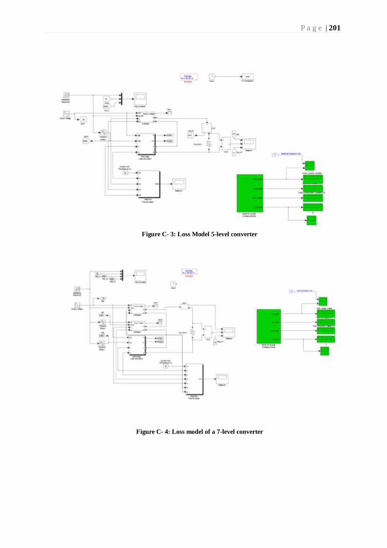
P a g e | 201
Figure C- 3: Loss Model 5-level converter
Figure C- 4: Loss model of a 7-level converter
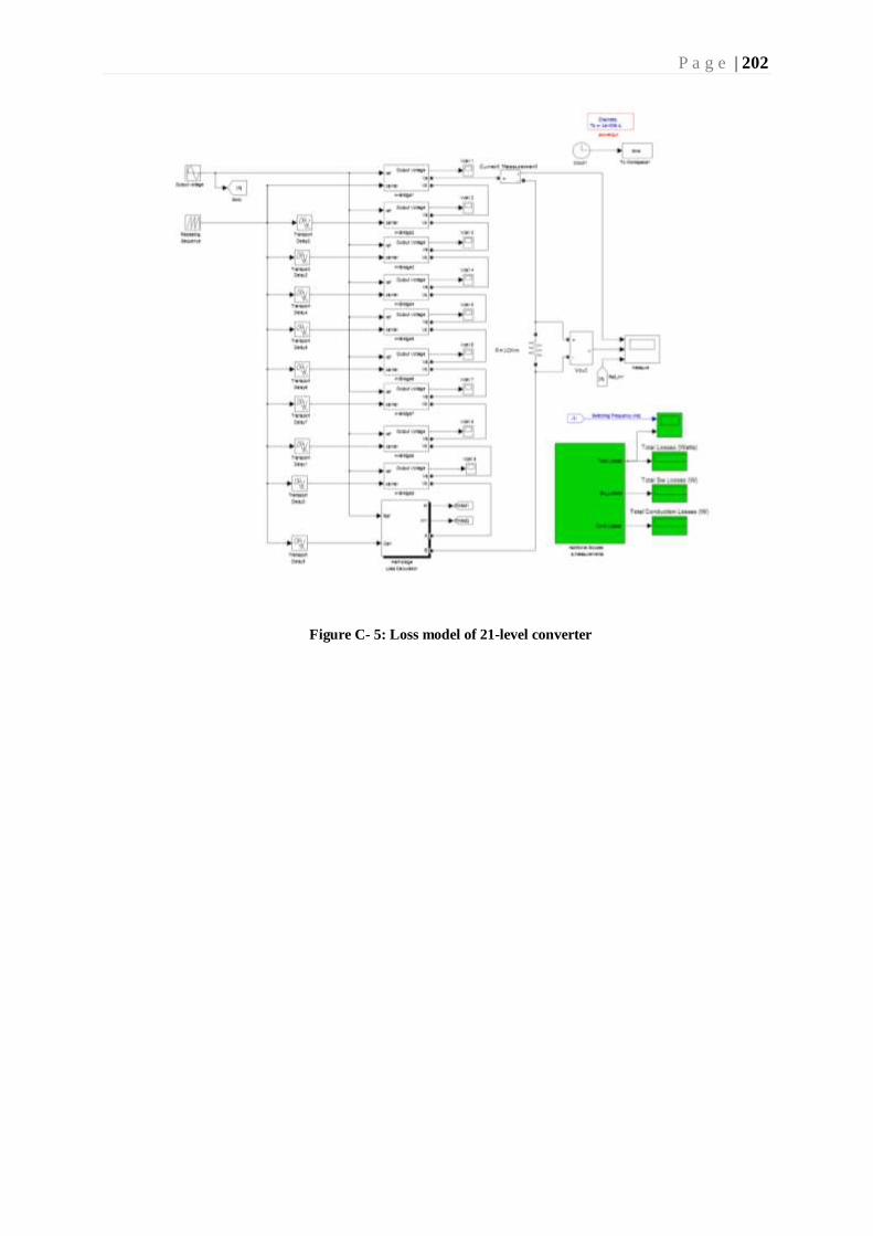
P a g e | 202
Figure C- 5: Loss model of 21-level converter
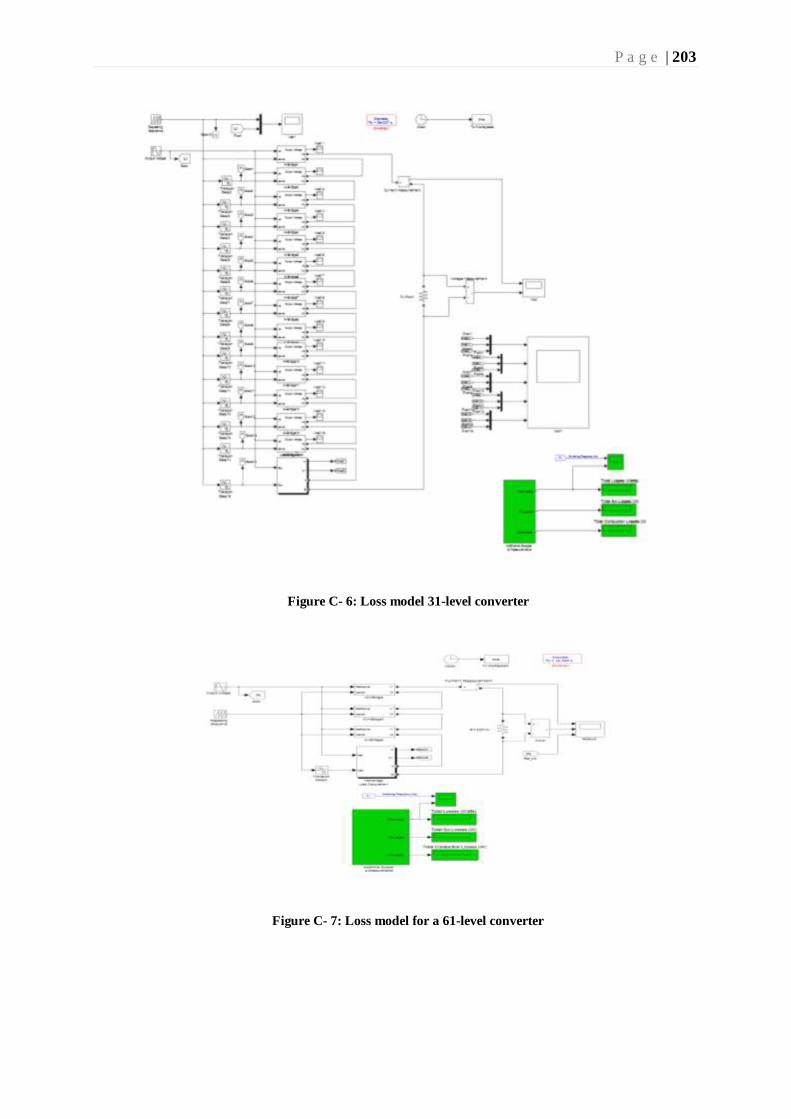
P a g e | 203
Figure C- 6: Loss model 31-level converter
Figure C- 7: Loss model for a 61-level converter
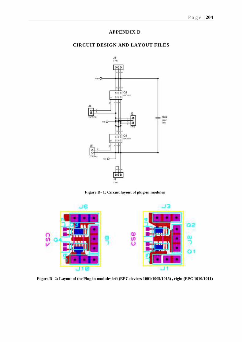
P a g e | 204
APPENDIX D
CIRCUIT DESIGN AND LAYOUT FILES
Figure D- 1: Circuit layout of plug-in modules
Figure D- 2: Layout of the Plug in modules left (EPC devices 1001/1005/1015) , right (EPC 1010/1011)

P a g e | 205
Figure D- 3: Implementation of the Plug-in-modules in an H-Bridge Circuit
Figure D- 4: Circuit diagram for the high side devices
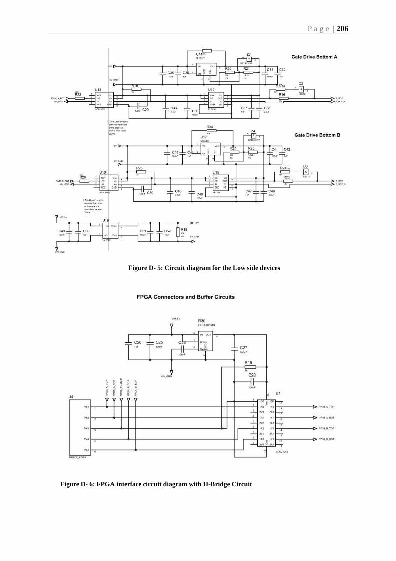
P a g e | 206
Figure D- 5: Circuit diagram for the Low side devices
Figure D- 6: FPGA interface circuit diagram with H-Bridge Circuit

P a g e | 207
Figure D- 7: Circuit diagram to the external interface circuit
Figure D- 8: Stencil used to allow uniform spread of solder
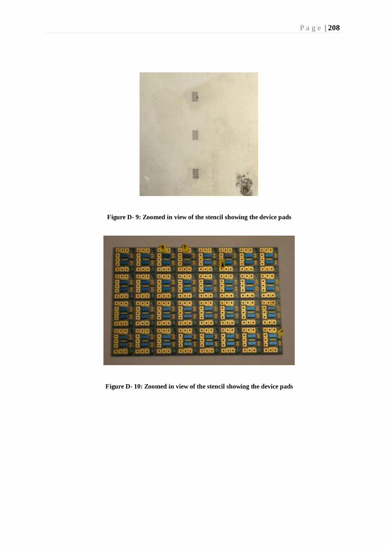
P a g e | 208
Figure D- 9: Zoomed in view of the stencil showing the device pads
Figure D- 10: Zoomed in view of the stencil showing the device pads
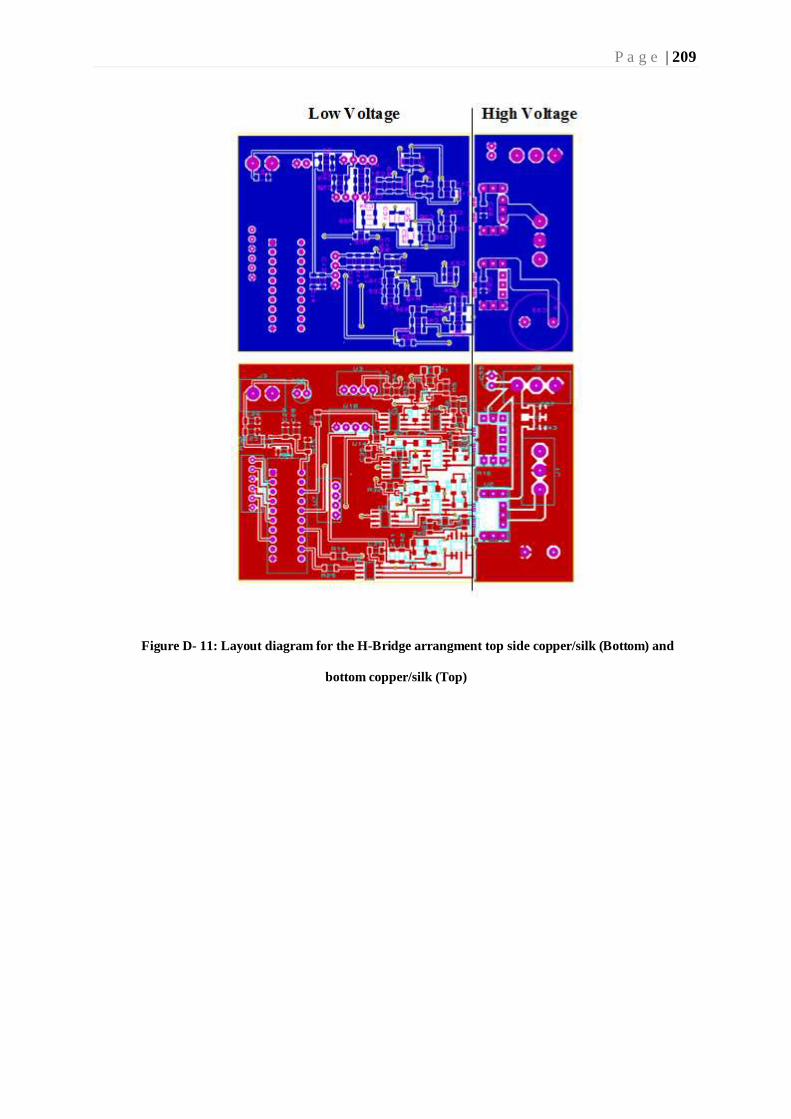
P a g e | 209
Figure D- 11: Layout diagram for the H-Bridge arrangment top side copper/silk (Bottom) and
bottom copper/silk (Top)
Related Documents


