1 Notes on Modulation techniques by Davide Micheli

Welcome message from author
This document is posted to help you gain knowledge. Please leave a comment to let me know what you think about it! Share it to your friends and learn new things together.
Transcript

1
Notes on Modulation techniques
by
Davide Micheli
2
Table of Contents
NOTES ON MODULATION TECHNIQUES.......................................................................................................... 1 TABLE OF CONTENTS................................................................................................................................................2
1 CANNEL CAPACITY AND IDEAL COMMUNICATION SYSTEMS ...................................................... 6 1.1 CHANNEL CAPACITY DEFINITION.................................................................................................................6
2 CODING........................................................................................................................................................... 14 2.1 CODE PERFORMANCE ................................................................................................................................14 2.2 SPECTRAL EFFICIENCY..............................................................................................................................12
3 INTERSYMBOL INTERFERENCE ............................................................................................................. 19 3.1 SPECTRAL PROPERTY REMINDER (SQUARE WAVE SPECTRUM) ...................................................................22 3.2 EQUALIZING FILTER ..................................................................................................................................23 3.3 NYQUIST’S FIRST METHOD (ZERO ISI) .....................................................................................................25 3.4 RAISED COSINE-ROLLOFF NYQUIST FILTERING ........................................................................................28
4 BANDPASS SIGNALING............................................................................................................................... 32 4.1 COMPLEX ENVELOPE RAPPRESTNATION OF BANDPASS WAVEFORMS ................................32
4.1.1 Definitions: Baseband, Bandpass, and modulation ............................................................................. 32 4.1.2 Complex Envelope Representation ...................................................................................................... 33 4.1.3 Theorem............................................................................................................................................... 33
4.2 REPRESENTATION OF MODULATED SIGNALS..............................................................................35 4.3 SPECTRUM OF BANDPASS SIGNALS................................................................................................36
Theorem ............................................................................................................................................................. 36 5 AM, FM, PM MODULATED SYSETMS.................................................................................................... 37
5.1 DEFINITIONS .............................................................................................................................................37 5.2 AMPLITUDE MODULATION ...............................................................................................................37
5.2.1 Normalized AM average power ........................................................................................................... 39 5.2.2 Definition: The modulation efficiency ................................................................................................. 40
6 PHASE MODULATION AND FREQUENCY MODULATION................................................................ 41 6.1 REPRESENTATION OF PM AND FM SIGNALS .............................................................................................41
6.1.1 Definition for peak phase deviation and peak frequency deviaton. ..................................................... 45 6.2 SPECTRA OF ANGLE-MODULATED SIGNALS ..............................................................................................46
6.2.1 Spectrum of a PM or FM signal with Sinusoidal Modulation ............................................................. 47 6.3 NOISE AND FREQUENCY MODULATION ......................................................................................................51
6.3.1 Noise triangle ...................................................................................................................................... 51 6.4 PREEMPHASIS AND DEEMPHASIS IN ANGLE MODULATED SYSTEMS...........................................................52
6.4.1 De-Emphasis response table................................................................................................................ 54 6.4.2 Why use “Roofed” Pre-Enhasis .......................................................................................................... 55
6.5 FREQUENCY DIVISION MULTIPLEXING.......................................................................................................55 7 OUTPUT SIGNAL-TO NOISE RATIOS FOR ANALOG SYSTEMS....................................................... 57
7.1 COMPARISON WITH BASEBAND SYSTEMS .................................................................................................58 7.2 AM SYSTEMS WITH PRODUCT DETECTION................................................................................................59 7.3 SSB SYSTEMS............................................................................................................................................60 7.4 PM SYSTEMS .............................................................................................................................................60 7.5 FM SYSTEMS ............................................................................................................................................62

3
7.6 FM SYSTEMS WITH THRESHOLD EXTENSION ............................................................................................63 7.7 FM SYSTEM WITH DE-EMPHASIS...............................................................................................................66
8 COMPARISON OF ANALOG SIGNALING SYSTEMS............................................................................ 67 8.1 IDEAL SYSTEMS PERFORMANCE.................................................................................................................68
9 BINARY MODULATED BANDPASS SIGNALING................................................................................... 70 9.1 BINARY PHASE-SHIFT KEYING (BPSK) ....................................................................................................71
9.1.1 BPSK Generation ................................................................................................................................ 71 9.1.2 BPSK Detection by a Correlation Receiver......................................................................................... 78 9.1.3 With Noise ........................................................................................................................................... 80
9.2 MAXIMUM LIKELIHOOD DETECTION.........................................................................................................83 9.3 BIT ERRORS ..............................................................................................................................................83
9.3.1 Q-Function reminder ........................................................................................................................... 85 9.3.2 Bit Error Probability in terms of Eb and N0......................................................................................... 87
10 DIFFERENTIAL PHASE-SHIFT KEYING (DPSK)................................................................................... 89 10.1 DIFFERENTIAL CODING..............................................................................................................................90
11 FREQUENCY SHIFT KEYING (FSK)......................................................................................................... 91 11.1 DISCONTINUOUS FSK ...............................................................................................................................91 11.2 CONTINUOUS FSK.....................................................................................................................................92 11.3 FSK DETECTION........................................................................................................................................93
12 MULTILEVEL MODULATED BANDPASS SIGNALING ....................................................................... 95 12.1 QUADRATURE PHASE-SHIFT KEYNG (QPSK) AND M-ARY PHASE-SHIFT KEYNG (MPSK) .......................95 12.2 OQPSK AND π/4 QPSK ..........................................................................................................................102 12.3 QUADRATURE AMPLITUDE MODULATION (QAM)..................................................................................106 12.4 PSD FOR MPSK, QAM, OQPSK, AND π/4 QPSK WITHOUT PRE-MODULATION FILTERING ....................107 12.5 SPECTRAL EFFICIENCY FOR MPSK, QAM,OQPSK, AND π/4 QPSK WITH RAISED COSINE FILTERING...109 12.6 RECEIVER QPSK, MSK AND PERFORMANCE ..........................................................................................117
13 FEHER-PATENTED QUADRATURE PHASE-SHIFT KEING.............................................................. 121 13.1 INTRODUCTION........................................................................................................................................121 13.2 SIGNAL MODEL FOR FQPSK ...................................................................................................................121 13.3 SIGNAL MODEL FOR FQPSK-B................................................................................................................131 13.4 SPECTRAL EFFICIENCY COMPARISON.......................................................................................................133
14 EFFICIENT MODULATION METHODS STUDY AT NASA/JPL ........................................................ 135 14.1 FQPSK-B MODULATION BIT-ERROR-RATE (BER) ................................................................................135 14.2 FQPSK-B MODULATION SPECTRA .........................................................................................................136
14.2.1 Hardware Spectrum Measurements.............................................................................................. 136 14.3 FQPSK-B MODULATION POWER CONTAINMENT ...................................................................................138 14.4 FQPSK-B MODULATION STUDY CONCLUSIONS .....................................................................................138
15 SUMMARY, CONCLUSIONS, AND RECOMMENDATIONS............................................................... 140 15.1.1 SUMMARY.................................................................................................................................... 140
15.2 CONCLUSIONS....................................................................................................................................144 15.2.1 Filtering Conclusions.................................................................................................................... 144 15.2.2 Loss Conclusions .......................................................................................................................... 145 15.2.3 Modulation Methods Conclusions ................................................................................................ 146 15.2.4 Spectrum Improvement Conclusions............................................................................................. 147
15.3 RECOMMENDATIONS .......................................................................................................................147 15.3.1 Mission Classification................................................................................................................... 147
16 8PSK MODULATION (EXAMPLE IMPLEMENTED IN MOBILE TELEPHONE NETWORK)..... 151 16.1 INTRODUCTION........................................................................................................................................151 16.2 EDGE SIGNAL DESCRIPTION: MODULATING SYMBOL RATE AND SYMBOL MAPPING .............................153
4
16.3 SYMBOL ROTATION.................................................................................................................................158 16.4 (8PSK EDGE) MODULATION AM DISTORTION .......................................................................................165
16.4.1 First problem (ISI):....................................................................................................................... 165 16.4.2 Second problem (AM):.................................................................................................................. 166
16.5 USED GAUSSIAN EDGE FILTER ..............................................................................................................167 16.6 EFFECT DUE TO GAUSSIAN EDGE FILTERING IN 3Π/8 SHIFTED 8PSK .....................................................170 16.7 MODULATION..........................................................................................................................................173 16.8 CONCLUSION...........................................................................................................................................173
17 EFFICIENT MODULATION METHODS STUDY AT NASA/JPL ........................................................ 174 17.1 PHASE SHIFT KEYED (8-PSK) MODULATION ...............................................................................174 17.2 PSK MODULATION BIT-ERROR-RATE (BER) .........................................................................................174 17.3 8-PSK MODULATION SPECTRA ...............................................................................................................175 17.4 PSK MODULATION POWER CONTAINMENT.............................................................................................177 17.5 PSK MODULATION STUDY CONCLUSIONS ..............................................................................................177
18 MINIMUM-SHIFT KEYNG (MSK) AND GMSK ..................................................................................... 178 18.1 GMSK ....................................................................................................................................................185
18.1.1 How to implement GMSK modulator............................................................................................ 190 18.1.2 How to implement GMSK demodulator ........................................................................................ 192
19 EFFICIENT MODULATION METHODS STUDY AT NASA/JPL ........................................................ 194 19.1 MSK AND GMSK MODULATION BIT-ERROR-RATE (BER) ....................................................................194 19.2 MSK AND GMSK MODULATION SPECTRA .............................................................................................194 19.3 MSK / GMSK MODULATION POWER CONTAINMENT .............................................................................196 19.4 MSK / GMSK MODULATION STUDY CONCLUSIONS...............................................................................197
20 HISTORY OF SPECTRUM EFFICIENT MODULATION IN TELEMETRY APPLICATIONS....... 198 21 CORRELATED DETECTION .................................................................................................................... 201 22 INTRODUCTION TO CDMA ..................................................................................................................... 206
22.1 MULTIPLE ACCESS ..................................................................................................................................206 22.2 SPREAD SPECTRUM MODULATION ...........................................................................................................207 22.3 TOLERANCE TO NARROWBAND INTERFERENCE ......................................................................................210 22.4 DIRECT SEQUENCE SPREAD SPECTRUM SYSTEM.....................................................................................211
22.4.1 Channelization operation.............................................................................................................. 212 22.4.2 Scrambling operation.................................................................................................................... 214
22.5 ORTHOGONAL SEQUENCES REMINDER.....................................................................................................214 22.6 MODULATION AND TOLERANCE TO WIDEBAND INTERFERENCE .............................................................216 22.7 UPLINK MODULATION.............................................................................................................................219
22.7.1 One UL parallel channel .............................................................................................................. 223 22.7.2 Two UL parallel channel .............................................................................................................. 225 22.7.3 Three UL parallel channel............................................................................................................ 230 22.7.4 Filtering ........................................................................................................................................ 236
22.8 DOWNLINK SPREADING AND MODULATION ............................................................................................238 22.8.1 Downlink Spreading Codes........................................................................................................... 238
23 ORTHOGONAL FREQUENCY DIVISION MULTIPLEXING (OFDM) .............................................. 241 23.1 INTRODUCTION........................................................................................................................................241 23.2 DIGITAL AUDIO BROADCASTING.............................................................................................................242 23.3 DIGITAL VIDEO BROADCASTING.............................................................................................................243 23.4 BASIC PRINCIPLE OF OFDM....................................................................................................................244 23.5 ORTHOGONALITY....................................................................................................................................246
23.5.1 FREQUENCY DOMAIN ORTHOGONALITY.............................................................................. 249 23.6 OFDM GENERATION AND RECEPTION .....................................................................................................250
23.6.1 Serial To Parallel Conversion ...................................................................................................... 251 23.6.2 Subcarrier modulation and mapping ............................................................................................ 252 23.6.3 Frequency to time domain conversion .......................................................................................... 253

5
23.7 OFDM TRANSMITTER.............................................................................................................................254 23.8 FFT(LINE SPECRA FOR PERIODIC WAVEFORMS).....................................................................................256
23.8.1 Theorem ........................................................................................................................................ 256 23.8.2 Theorem ........................................................................................................................................ 258
24 APPENDIX..................................................................................................................................................... 267 24.1 CONVOLUTION PROCESS..........................................................................................................................267 24.2 DIRAC DELTA FUNCTION AND CONVOLUTION PROCESS ...........................................................................270
25 REFERENCE................................................................................................................................................. 271
6
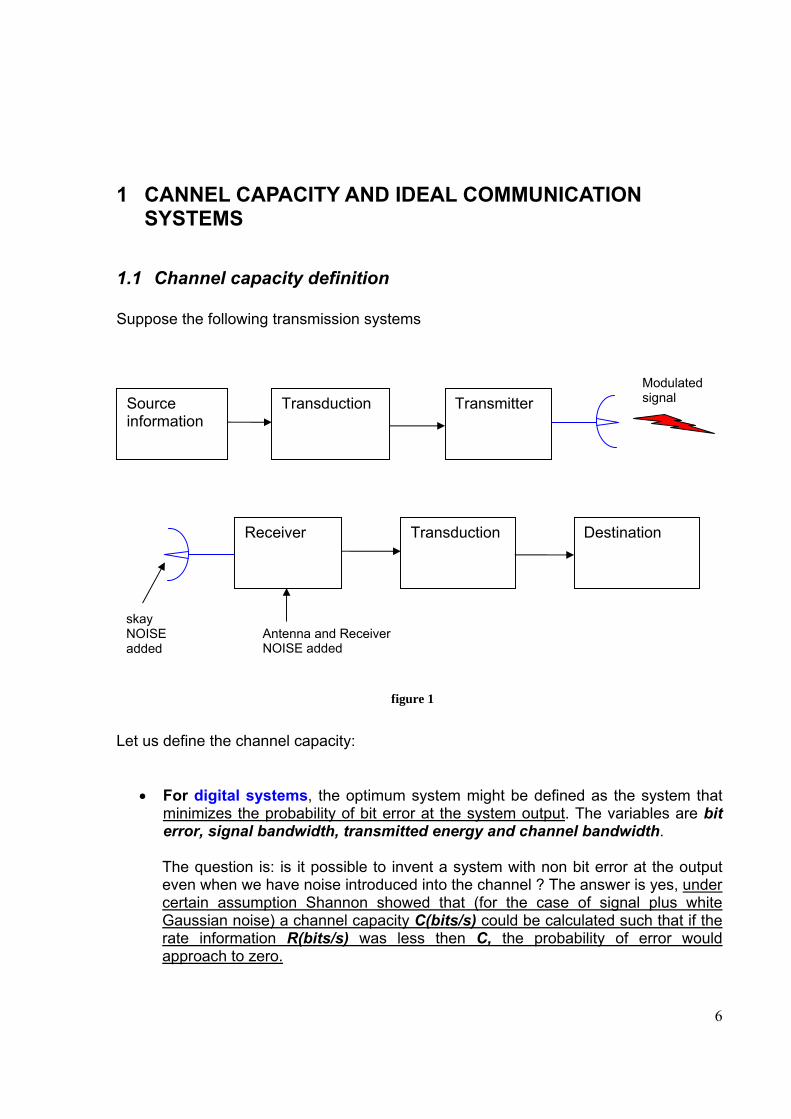
1 CANNEL CAPACITY AND IDEAL COMMUNICATION SYSTEMS
1.1 Channel capacity definition Suppose the following transmission systems
figure 1
Let us define the channel capacity:
• For digital systems, the optimum system might be defined as the system that minimizes the probability of bit error at the system output. The variables are bit error, signal bandwidth, transmitted energy and channel bandwidth.
The question is: is it possible to invent a system with non bit error at the output even when we have noise introduced into the channel ? The answer is yes, under certain assumption Shannon showed that (for the case of signal plus white Gaussian noise) a channel capacity C(bits/s) could be calculated such that if the rate information R(bits/s) was less then C, the probability of error would approach to zero.
Transduction Source information
Antenna and Receiver NOISE added
Transmitter
Destination Receiver Transduction
skay NOISE added
Modulated signal
7
⎟⎠⎞
⎜⎝⎛ +=
NSBC 1log2 eq 1
where B is the channel bandwidth in (Hz) and S/N is the signal-to-noise power ratio(watts/watts, no dB) at the input to the digital receiver.
Shannon gives us a theoretical performance bound that we can strive to achieve with practical communication systems. Systems that approach this bound usually incorporate error correction coding.
• In analog systems, in place of error probability, the optimum system might be
defined as the one that achieves the largest signal-to-noise ratio at the receiver output, subject to design constraints such as channel bandwidth and transmitted power.
In this case the question is: is it possible to design a system with infinite signal to noise ratio at the output when noise is introduced to the channel ? The answerer is no.
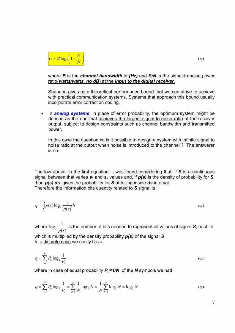
The law above, in the first equation, it was found considering that: if S is a continuous signal between that varies s1 and s2 values and, if p(s) is the density of probability for S, than p(s)⋅ds gives the probability for S of felling inside ds interval. Therefore the information bits quantity related to S signal is
dssp
spqs
s∫=2
1)(
1log)( 2 eq 2
where )(
1log2 sp is the number of bits needed to represent all values of signal S, each of
which is multiplied by the density probability p(s) of the signal S In a discrete case we easily have:
∑=
=N
n nn P
Pq1
21log eq 3
where in case of equal probability Pn=1/N of the N symbols we had
∑ ∑ ∑= = =
====N
n
N
n
N
nnn NN
NN
NPPq
1 1 12222 loglog1log11log eq 4
8
As an example the representation of 8 states discrete signal, where all states are supposed with the same probability, require 3 bits (each bit can assume 2 values high, low so we using log2x) because
8log3 2= eq 5
In the continuous scenario, if S is the average signal and σ2 is the variance, then it can be shown that q (the number of bits needed to represent S) became maximum when p(s) has a Gaussian distribution probability:
2
2
2)(
2
2
πσ
σS
esp−
= eq 6
In this case the bound of S are: s1=-∞ , s2=∞. The corresponding quantity of information q (number of bits needed to represent S ) can be obtained substituting this equation in the integral, above:
ebits/sampl )2(log21)2(log
2
1log)( 22
21
22
2
2
22
2 eSeSds
e
spqS
ππ
πσ
σ
=== ∫∞
∞− − eq 7
here S2 is the average signal power. Considering now the Shannon theorem which says that a signal of bandwidth B requires at least 2B sample rate (samples/second). Therefore in a time interval t are necessary 2B⋅t samples of the signal S, here each sample are univocally determined by q bits. So the information quantity bit related to the sampled signal S with q bits quantizing, on the time interval t is:
bits )2(log)2(log22 22
21
22 eSBteSBtqtBQ ππ ==⋅⋅= eq 8
The presence of noise corrupts the receiving information at the receiver input. The relative information associated is:
bits )2(log2)2(log)2(log22 22
221
22 NN ePBteSBteSBtqtBQ πππ ===⋅⋅= eq 9
where PN= 2S is the average noise power . Then at the input of the receiver we have the noise power PN along with the information power signal PS:
9
( )[ ]{ } bits 2log2 2 NSNSNS PPeBtqtBQ +=⋅⋅= ++ π eq 10 where PS+PN =S2 is the total power of signal plus noise with Gaussian probability density function The uncorrupted quantity of information will be
( )[ ] ( )[ ]{ }( )( ) bits 1log
22log
2log2log2
22
22
PPt B
PePPet B
PePPetBqtBQQQ
N
S
N
NS
NNSNSNNS
⎟⎟⎠
⎞⎜⎜⎝
⎛+⋅=
+⋅=
=−+⋅=⋅⋅=−= ++
ππ
ππ
eq 11
The bitrate Rb will be
bits/s 1log2 RPPB
tQ
bN
S =⎟⎟⎠
⎞⎜⎜⎝
⎛+= eq 12
we can invert the equation to find PS/PN
⎟⎟⎠
⎞⎜⎜⎝
⎛−= ⋅ 12 tB
Q
N
S
PP
eq 13
where
⎟⎟⎠
⎞⎜⎜⎝
⎛−=⇒⎟⎟
⎠
⎞⎜⎜⎝
⎛−=⇒= ⋅⋅ 12 12 tB
Q
StB
QS
N KTBPKTBPKTBP eq 14
This is the Hartely-Shannon law which contains the essential components of transmission systems:
1. bandwidth B 2. power of signal PS 3. power pf noise PN 4. duration of message t 5. temperature of reference T
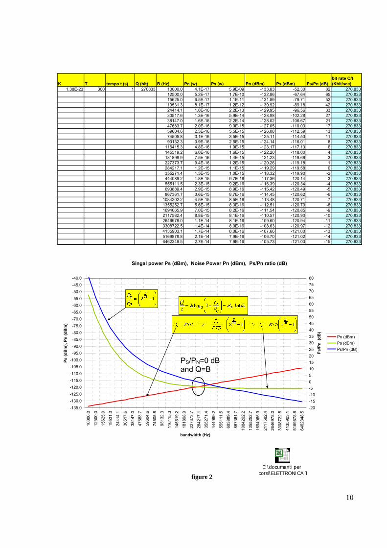
PS and PN power are reported in figure below as a function of the bandwidth, we have fixed T=300 (K), Q=270833 (bit), K=1.38*10-23 (J/K) , t= 1 (s)
10
PS/PN=0 dB and Q=B
K T tempo t (s) Q (bit) B (Hz) Pn (w) Ps (w) Pn (dBm) Ps (dBm) Ps/Pn (dB)bit rate Q/t (Kbit/sec)
1.38E-23 300 1 270833 10000.0 4.1E-17 5.9E-09 -133.83 -52.30 82 270.83312500.0 5.2E-17 1.7E-10 -132.86 -67.64 65 270.83315625.0 6.5E-17 1.1E-11 -131.89 -79.71 52 270.83319531.3 8.1E-17 1.2E-12 -130.92 -89.18 42 270.83324414.1 1.0E-16 2.2E-13 -129.95 -96.56 33 270.83330517.6 1.3E-16 5.9E-14 -128.98 -102.28 27 270.83338147.0 1.6E-16 2.2E-14 -128.02 -106.67 21 270.83347683.7 2.0E-16 9.9E-15 -127.05 -110.03 17 270.83359604.6 2.5E-16 5.5E-15 -126.08 -112.59 13 270.83374505.8 3.1E-16 3.5E-15 -125.11 -114.53 11 270.83393132.3 3.9E-16 2.5E-15 -124.14 -116.01 8 270.833
116415.3 4.8E-16 1.9E-15 -123.17 -117.13 6 270.833145519.2 6.0E-16 1.6E-15 -122.20 -118.00 4 270.833181898.9 7.5E-16 1.4E-15 -121.23 -118.66 3 270.833227373.7 9.4E-16 1.2E-15 -120.26 -119.18 1 270.833284217.1 1.2E-15 1.1E-15 -119.29 -119.58 0 270.833355271.4 1.5E-15 1.0E-15 -118.32 -119.90 -2 270.833444089.2 1.8E-15 9.7E-16 -117.36 -120.14 -3 270.833555111.5 2.3E-15 9.2E-16 -116.39 -120.34 -4 270.833693889.4 2.9E-15 8.9E-16 -115.42 -120.49 -5 270.833867361.7 3.6E-15 8.7E-16 -114.45 -120.62 -6 270.833
1084202.2 4.5E-15 8.5E-16 -113.48 -120.71 -7 270.8331355252.7 5.6E-15 8.3E-16 -112.51 -120.79 -8 270.8331694065.9 7.0E-15 8.2E-16 -111.54 -120.85 -9 270.8332117582.4 8.8E-15 8.1E-16 -110.57 -120.90 -10 270.8332646978.0 1.1E-14 8.1E-16 -109.60 -120.94 -11 270.8333308722.5 1.4E-14 8.0E-16 -108.63 -120.97 -12 270.8334135903.1 1.7E-14 8.0E-16 -107.66 -121.00 -13 270.8335169878.8 2.1E-14 7.9E-16 -106.70 -121.02 -14 270.8336462348.5 2.7E-14 7.9E-16 -105.73 -121.03 -15 270.833
Singal power Ps (dBm), Noise Power Pn (dBm), Ps/Pn ratio (dB)
-135.0-130.0-125.0-120.0-115.0-110.0-105.0-100.0-95.0-90.0-85.0-80.0-75.0-70.0-65.0-60.0-55.0-50.0-45.0-40.0
1000
0.0
1250
0.0
1562
5.0
1953
1.3
2441
4.1
3051
7.6
3814
7.0
4768
3.7
5960
4.6
7450
5.8
9313
2.3
1164
15.3
1455
19.2
1818
98.9
2273
73.7
2842
17.1
3552
71.4
4440
89.2
5551
11.5
6938
89.4
8673
61.7
1084
202.
2
1355
252.
7
1694
065.
9
2117
582.
4
2646
978.
0
3308
722.
5
4135
903.
1
5169
878.
8
6462
348.
5
bandwidth (Hz)
Ps (d
Bm
), Pn
(dB
m)
-20-15-10-505101520253035404550556065707580
Ps/P
n (d
B)
Pn (dBm)Ps (dBm)Ps/Pn (dB)
figure 2 E:\documenti per
corsi\ELETTRONICA T
11
we can get some note:
• By equation 11 we can observe that the information Q(n°bit) remains constant if the product B⋅t is constant, the exchange between B and t is used in satellite application. In fact the data can be collected, along the orbit, with low B and high period of time t, the data are stored by using a memory device. After, the transmission of data stored before, is possible only in a short period when the satellite is flying above the Earth Station, by using a great bandwidth B.
• The bit-rate Q/t (bit/s) remain constant increasing the bandwidth and simultaneously reducing the PS/PN ratio, this represent a possible application in spread spectrum communication system, the greater the bandwidth the lower PS/PN ratio. Anyway if we are increasing the bandwidth, then the power of the signal PS will reduce to tend asymptotically to a constant while PN will increases more. When
112 =⎟⎟⎠
⎞⎜⎜⎝
⎛−= ⋅tB
Q
N
S
PP
eq 15
i.e. where
( ) bits/s 11log1log 22 RBBPPB
tQ
bN
S ==+=⎟⎟⎠
⎞⎜⎜⎝
⎛+= eq 16
Therefore when PS=PN, then the maximum transmission bandwidth (Hz) needed for a correct received signal, is the same order of the channel capacity (bit/s).
Onboard of a satellite, one of the main problems concerns the heavy of the transmitter systems, and the power required to transmission signaling. Therefore we are looking for a system which can beneficial of exchanging between (PS/PN) and bandwidth between input and output of the receiver. In frequency modulation systems the bandwidth of the carrier channels are greater than RX_output bandwidth channel, so at the input of the receiver can be used a lower PS/PN. Anyway FM must work above FM C/N threshold and since the greater the bandwidth, the greater the noise, then C/N threshold will increase with bandwidth. As a consequence the Carrier power C will be affected by the same amount of growth too, resulting in a bigger amplifier rather then a little amplifier as required. As a conclusion, once we have been fixed PS/PN and the bit_rate Q/t, then we can observe that the lower the PN, the lower PS. So the very important component of a transmission design is trying to reducing the noise power PN.
12
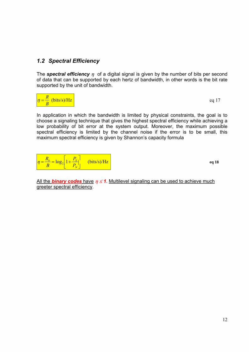
1.2 Spectral Efficiency The spectral efficiency η of a digital signal is given by the number of bits per second of data that can be supported by each hertz of bandwidth, in other words is the bit rate supported by the unit of bandwidth.
z(bits/s)/H BR
=η eq 17
In application in which the bandwidth is limited by physical constraints, the goal is to choose a signaling technique that gives the highest spectral efficiency while achieving a low probability of bit error at the system output. Moreover, the maximum possible spectral efficiency is limited by the channel noise if the error is to be small, this maximum spectral efficiency is given by Shannon’s capacity formula
z(bits/s)/H 1log2 PP
BRη
N
Sb⎥⎦
⎤⎢⎣
⎡+== eq 18
All the binary codes have η ≤ 1. Multilevel signaling can be used to achieve much greeter spectral efficiency.
13
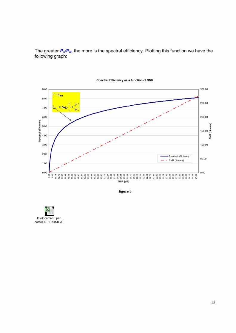
The greater Ps/PN, the more is the spectral efficiency. Plotting this function we have the following graph:
Spectral Efficiency as a function of SNR
0.00
1.00
2.00
3.00
4.00
5.00
6.00
7.00
8.00
9.00
0.00
8.45
11.1
412
.79
13.9
814
.91
15.6
816
.33
16.9
017
.40
17.8
518
.26
18.6
318
.98
19.2
919
.59
19.8
720
.13
20.3
720
.61
20.8
321
.04
21.2
421
.43
21.6
121
.79
21.9
622
.12
22.2
822
.43
22.5
822
.72
22.8
622
.99
23.1
223
.24
23.3
623
.48
23.6
023
.71
23.8
223
.93
24.0
324
.13
24.2
324
.33
SNR (dB)
Spec
tral
effi
cien
cy
0.00
50.00
100.00
150.00
200.00
250.00
300.00
SNR
(Lin
eare
)
Spectral efficiencySNR (lineare)
figure 3
E:\documenti per corsi\ELETTRONICA T
14
2 CODING If the data at the output of a digital communication system have errors that are too frequent for the desired use, the errors can be often reduced by use either of two main techniques:
• Automatic repeat request (ARQ) • Forward error correction (FEC)
In an ARQ system, when a receiver circuit detects parity errors in a block of data, it requests that the data block be retransmitted. In FEC system, the transmitted data are encoded so that the receiver can correct, as well as detect errors. These procedures are also classified as channel coding because they are used to correct errors caused by channel noise. This is different from source coding, where the purpose of coding is to extract the essential information from the source and encode it into digital form so that it can be efficiently stored or transmitted using a digital techniques (example PCM) The choice between using the ARQ or the FEC technique depends on the particular application.
• ARQ is often used in computer communication systems because is relatively inexpensive to implement and there is usually a duplex (two-way) channel so that the receiving and can transmit back an acknowledgement (ACK) for correctly received data or a requests for retransmission (NAC) when the data are received in error.
• FEC is preferred on systems with large retransmission delays because if the ARQ technique were used, the effective data rate would be small; the transmitter would have long periods while waiting for the ACK/NAC indicator, which is retarded by the long transmission delay.
2.1 Code performance The improvement in the performance of a digital communication system can be achieved by the use of coding as illustrated below:
15
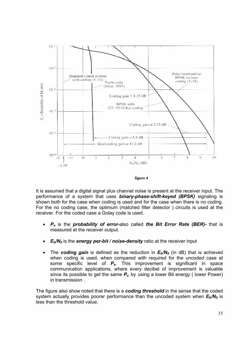
figure 4
It is assumed that a digital signal plus channel noise is present at the receiver input. The performance of a system that uses binary-phase-shift-keyed (BPSK) signaling is shown both for the case when coding is used and for the case when there is no coding. For the no coding case, the optimum (matched filter detector ) circuits is used at the receiver. For the coded case a Golay code is used.
• Pe is the probability of error-also called the Bit Error Rate (BER)- that is measured at the receiver output.
• Eb/N0 is the energy per-bit / noise-density ratio at the receiver input
• The coding gain is defined as the reduction in Eb/N0 (in dB) that is achieved
when coding is used, when compared with required for the uncoded case at some specific level of Pe. This improvement is significant in space communication applications, where every decibel of improvement is valuable since its possible to get the same Pe by using a lower Bit energy ( lower Power) in transmission .
The figure also show noted that there is a coding threshold in the sense that the coded system actually provides poorer performance than the uncoded system when Eb/N0 is less than the threshold value.
16
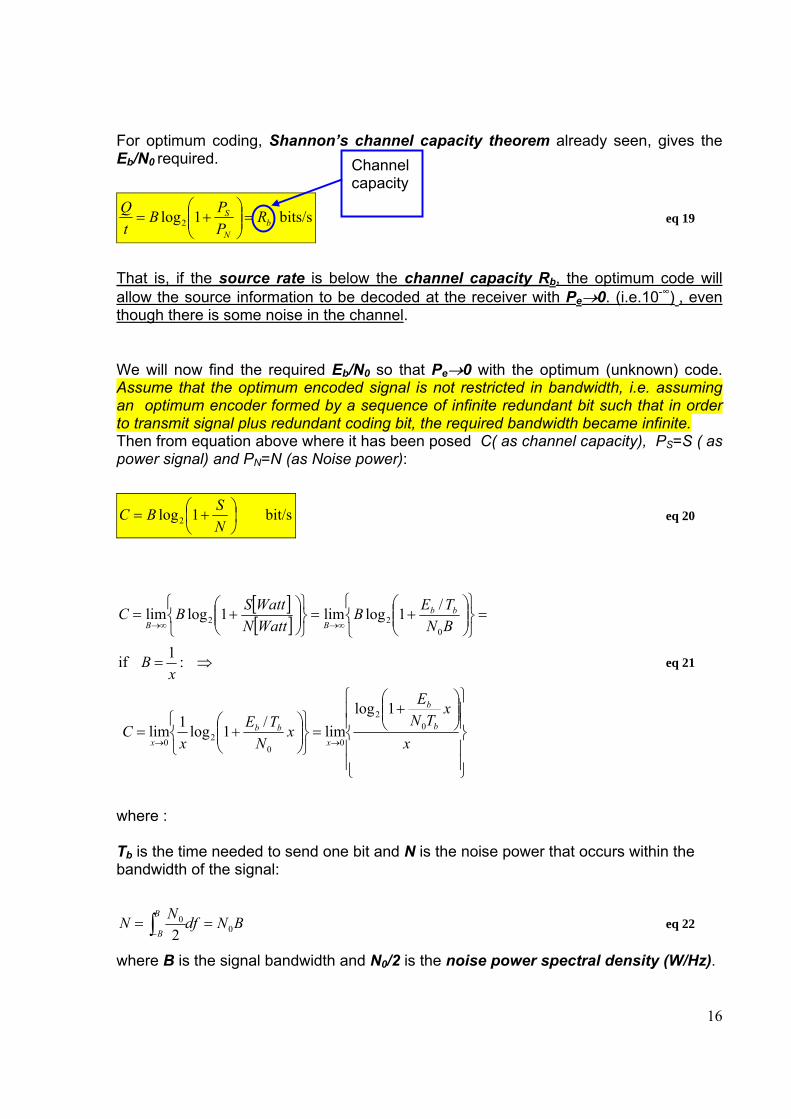
For optimum coding, Shannon’s channel capacity theorem already seen, gives the Eb/N0 required.
bits/s 1log2 RPPB
tQ
bN
S =⎟⎟⎠
⎞⎜⎜⎝
⎛+= eq 19
That is, if the source rate is below the channel capacity Rb, the optimum code will allow the source information to be decoded at the receiver with Pe→0. (i.e.10-∞) , even though there is some noise in the channel. We will now find the required Eb/N0 so that Pe→0 with the optimum (unknown) code. Assume that the optimum encoded signal is not restricted in bandwidth, i.e. assuming an optimum encoder formed by a sequence of infinite redundant bit such that in order to transmit signal plus redundant coding bit, the required bandwidth became infinite. Then from equation above where it has been posed C( as channel capacity), PS=S ( as power signal) and PN=N (as Noise power):
bit/s 1log2 ⎟⎠⎞
⎜⎝⎛ +=
NSBC eq 20
[ ][ ]
⎪⎪⎭
⎪⎪⎬
⎫
⎪⎪⎩
⎪⎪⎨
⎧⎟⎟⎠
⎞⎜⎜⎝
⎛+
=⎭⎬⎫
⎩⎨⎧
⎟⎟⎠
⎞⎜⎜⎝
⎛+=
⇒=
=⎭⎬⎫
⎩⎨⎧
⎟⎟⎠
⎞⎜⎜⎝
⎛+=
⎭⎬⎫
⎩⎨⎧
⎟⎟⎠
⎞⎜⎜⎝
⎛+=
→→
→∞→∞
x
xTN
E
xN
TEx
C
xB
BNTEB
WattNWattSBC
b
b
xbb
x
bbBB
02
00
20
022
1loglim/1log1lim
:1 if
/1loglim1loglim
eq 21
where : Tb is the time needed to send one bit and N is the noise power that occurs within the bandwidth of the signal:
BNdfNNB
B 00
2== ∫− eq 22
where B is the signal bandwidth and N0/2 is the noise power spectral density (W/Hz).
Channel capacity

17
L’ Hospital’s rule is used to evaluate this limit:
( )2ln
12ln
lnlog1
log1
1
lim
1loglim
002
0
20
0
0
02
0
b
b
b
b
b
b
b
b
b
b
x
b
b
x
TNEe
TNEe
TNE
eTN
E
xTN
E
xx
xTN
Ex
C
=⎟⎠⎞
⎜⎝⎛==
⎪⎪⎪
⎭
⎪⎪⎪
⎬
⎫
⎪⎪⎪
⎩
⎪⎪⎪
⎨
⎧
⎟⎟⎠
⎞⎜⎜⎝
⎛+
=
=
⎪⎪
⎭
⎪⎪
⎬
⎫
⎪⎪
⎩
⎪⎪
⎨
⎧
∂∂
⎥⎦
⎤⎢⎣
⎡⎟⎟⎠
⎞⎜⎜⎝
⎛+
∂∂
=
→
→
eq 23
where we have used the logarithm property of base changes
( ) ( )( ) ( ) ( )
( )( )( ) ( ) 2ln
1 2ln
ln2log
loglog logloglog 2 ===⇒=
eeeaxx
b
e
b
ba eq 24
and the derivative property of logarithm
( ) ( )
2ln1
2ln1
11log lim
ln1log
00
0
020
b
b
b
b
b
bb
bx
a
TNE
TNE
xTN
Ex
TNE
dxd
dxdu
auu
dxd
=
⎪⎪⎭
⎪⎪⎬
⎫
⎪⎪⎩
⎪⎪⎨
⎧
⎟⎟⎠
⎞⎜⎜⎝
⎛+
=⎥⎦
⎤⎢⎣
⎡⎟⎟⎠
⎞⎜⎜⎝
⎛+⇒
⇒⋅
=
→
eq 25
If we signal at a rate, approaching the channel capacity, then Pe→0, and we have the maximum information rate allowed for the Pe→0 (i.e. the optimum system). Thus
2ln
11
source ratebit re whe1
0
⇒=
==
b
b
b
bb
TNE
T
TT
C
eq 26
18
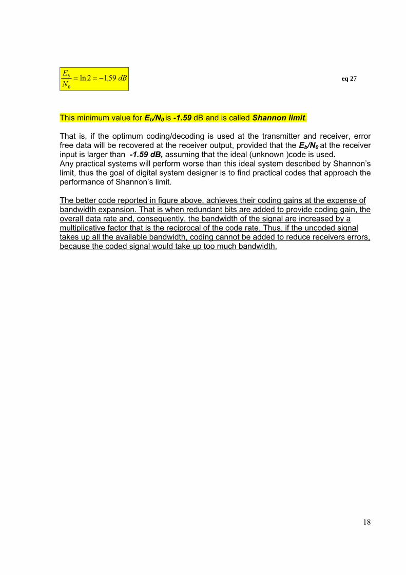
dB,NEb 5912ln
0
−== eq 27
This minimum value for Eb/N0 is -1.59 dB and is called Shannon limit. That is, if the optimum coding/decoding is used at the transmitter and receiver, error free data will be recovered at the receiver output, provided that the Eb/N0 at the receiver input is larger than -1.59 dB, assuming that the ideal (unknown )code is used. Any practical systems will perform worse than this ideal system described by Shannon’s limit, thus the goal of digital system designer is to find practical codes that approach the performance of Shannon’s limit. The better code reported in figure above, achieves their coding gains at the expense of bandwidth expansion. That is when redundant bits are added to provide coding gain, the overall data rate and, consequently, the bandwidth of the signal are increased by a multiplicative factor that is the reciprocal of the code rate. Thus, if the uncoded signal takes up all the available bandwidth, coding cannot be added to reduce receivers errors, because the coded signal would take up too much bandwidth.
19
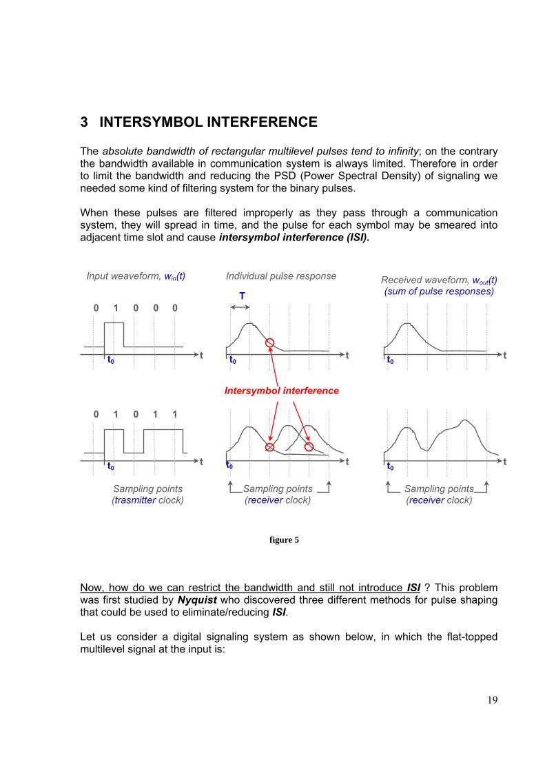
3 INTERSYMBOL INTERFERENCE The absolute bandwidth of rectangular multilevel pulses tend to infinity; on the contrary the bandwidth available in communication system is always limited. Therefore in order to limit the bandwidth and reducing the PSD (Power Spectral Density) of signaling we needed some kind of filtering system for the binary pulses. When these pulses are filtered improperly as they pass through a communication system, they will spread in time, and the pulse for each symbol may be smeared into adjacent time slot and cause intersymbol interference (ISI).
figure 5
Now, how do we can restrict the bandwidth and still not introduce ISI ? This problem was first studied by Nyquist who discovered three different methods for pulse shaping that could be used to eliminate/reducing ISI. Let us consider a digital signaling system as shown below, in which the flat-topped multilevel signal at the input is:
1 0 0
t
0 0
t0
Input weaveform, win(t)
1 1 1
t
0 0
t0
Sampling points (trasmitter clock)
tt0
Sampling points (receiver clock)
tt0
Sampling points (receiver clock)
Individual pulse response
tt0
Ts
tt0
Received waveform, wout(t) (sum of pulse responses)
Intersymbol interference
20
-0.4
-0.2
0
0.2
0.4
0.6
0.8
1
-20 -15 -10 -5 0 5 10 15 20
freq -Ts/2 Ts/2
1
t
2π/Ts
figure 6
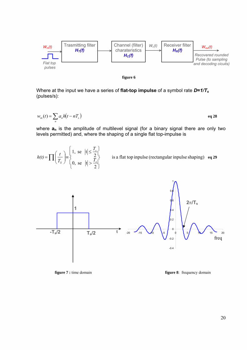
Where at the input we have a series of flat-top impulse of a symbol rate D=1/Ts (pulses/s):
( )∑ −=n
snin nTthatw )( eq 28
where an is the amplitude of multilevel signal (for a binary signal there are only two levels permitted) and, where the shaping of a single flat top-impulse is
shaping) inpulsear (rectangul inpulse flat top a is
2t se 0,
2t se 1,
⎪⎭
⎪⎬
⎫
⎪⎩
⎪⎨
⎧
>
≤≡⎟⎟
⎠
⎞⎜⎜⎝
⎛=∏
s
s
ST
T
Tth(t) eq 29
figure 7 : time domain figure 8: frequency domain
Trasmitting filter HT(f)
Channel (filter)charateristics
HC(f)
Receiver filter HR(f)
Win(t) Wout(t)Wc(t)
Flat top pulses
Recovered rounded Pulse (to sampling
and decoding cicuits)
21
0
0.1
0.2
0.3
0.4
0.5
0.6
0.7
0.8
0.9
1
-20 -15 -10 -5 0 5 10 15 20
The frequency domain of a single flat-top impulse is obtained by Fourier transform
2
22
2
2
2
11)(
2/2/2/2/
2/2/2/
2/
2/
2/
2/
2/
s
s
s
TjTj
ss
sTjTj
s
s
TjTjT
T
tjT
T
tjT
T
tj
T
TsenT
jee
TT
jee
T
T
jee
jedtej
jdtefH
ssss
sss
s
s
s
s
s
ω
ω
ωω
ωωω
ω
ωωωω
ωωωωω
⎟⎠⎞
⎜⎝⎛
=−
=−−
=
=−−
=⎥⎦
⎤⎢⎣
⎡−
=⋅−−
=⋅=
−++−
+−+
−
−
−
−
−
− ∫∫
eq 30
The PSD of single flat top impulse is then obtained by :
( )( )
2
2
22/2/22/
2/
22/
2/
22/
2/
2
2
2
2/2/
221
11)(
s
s
s
s
sTjTjT
T
tj
T
T
tjT
T
tj
T
TsenT
TT
jeee
j
dtejj
dtefH
sss
s
s
s
s
s
ω
ω
ωω
ωω
ωωω
ωω
⎟⎠⎞
⎜⎝⎛
=
=−−
=⎥⎦
⎤⎢⎣
⎡−
=
=⋅−−
=⋅=
−
−
−
−
−
−
− ∫∫
eq 31
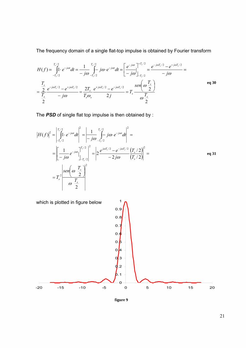
which is plotted in figure below
figure 9
22
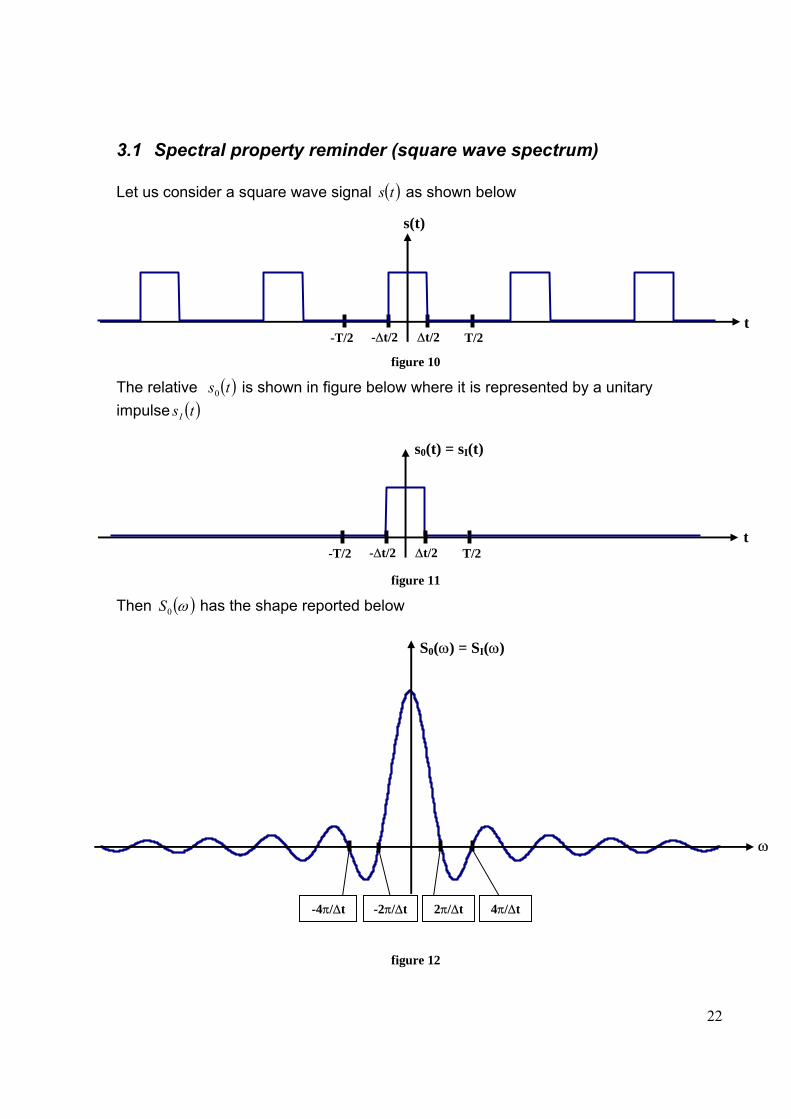
3.1 Spectral property reminder (square wave spectrum) Let us consider a square wave signal ( )ts as shown below
figure 10
The relative ( )ts0 is shown in figure below where it is represented by a unitary impulse ( )tsI
figure 11
Then ( )ω0S has the shape reported below
figure 12
s(t)
t -T/2 -∆t/2 T/2 ∆t/2
t
s0(t) = sI(t)
-T/2 -∆t/2 T/2 ∆t/2
S0(ω) = SI(ω)
ω
2π/∆t 4π/∆t-2π/∆t-4π/∆t
23
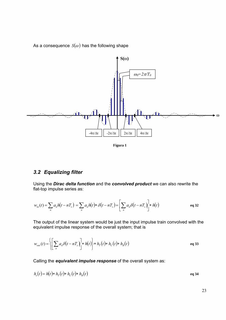
As a consequence ( )ωS has the following shape
Figura 1
3.2 Equalizing filter Using the Dirac delta function and the convolved product we can also rewrite the flat-top impulse series as:
( ) ( ) ( ) ( ) ( )thnTtanTtthanTthatw sn
nsn
nn
snin ∗⎥⎦
⎤⎢⎣
⎡−=−∗=−= ∑∑∑ δδ )( eq 32
The output of the linear system would be just the input impulse train convolved with the equivalent impulse response of the overall system; that is
( ) ( ) ( ) ( ) ( )ththththnTtatw RCTsn
nout ∗∗∗⎭⎬⎫
⎩⎨⎧
∗⎥⎦
⎤⎢⎣
⎡−= ∑ δ)( eq 33
Calling the equivalent impulse response of the overall system as:
( ) ( ) ( ) ( ) ( )ththththth RCTe ∗∗∗= eq 34
S(ω)
ω
2π/∆t 4π/∆t-2π/∆t-4π/∆t
ω0=2π/T0
24
then
( ) ( ) ( )sen
nesn
nout nTthathnTtatw −=∗⎥⎦
⎤⎢⎣
⎡−= ∑∑ δ)( eq 35
Note that he(t) is also the pulse shape that will appear at the output of the receiver filter when a single Dirac pulse is fed into the transmitting filter. The equivalent system transfer function is in frequency domain and it is represented by the product of the corresponding Fourier transform of each single element:
)()()()()( fHfHfHfHfH RCTe = eq 36
H(f) is the Fourier transform already seen that define the pulse shape
⎥⎥⎥⎥
⎦
⎤
⎢⎢⎢⎢
⎣
⎡⎟⎠⎞
⎜⎝⎛
=
2
2)(s
s
ss
s T
TsenTfH
ω
ω eq 37
Then the receiving filter is given by
)()()()()(
fHfHfHfHfH
CT
eR = eq 38
When He(f) is chosen to minimize the ISI, HR(f) is called an equalizing filter. The equalizing filter characteristic depends on Hc(f), the channel frequency response, as well as on the required He(f). When the channel consists of dial-up telephone lines, the channel transfer function changes from call to call and the equalizing filter may need to be an adaptive filter. In this case, the equalizing filter adjusts itself to minimize the ISI. In some adaptive schemes, each communication session is preceded by a test pattern that is used to adapt the filter electronically for the maximum eye opening (minimum ISI). Such sequence are called learning or training sequence and preambles. As an example of training sequence we report those used in GSM mobile network Um-Interface for a burst of 148 bits:
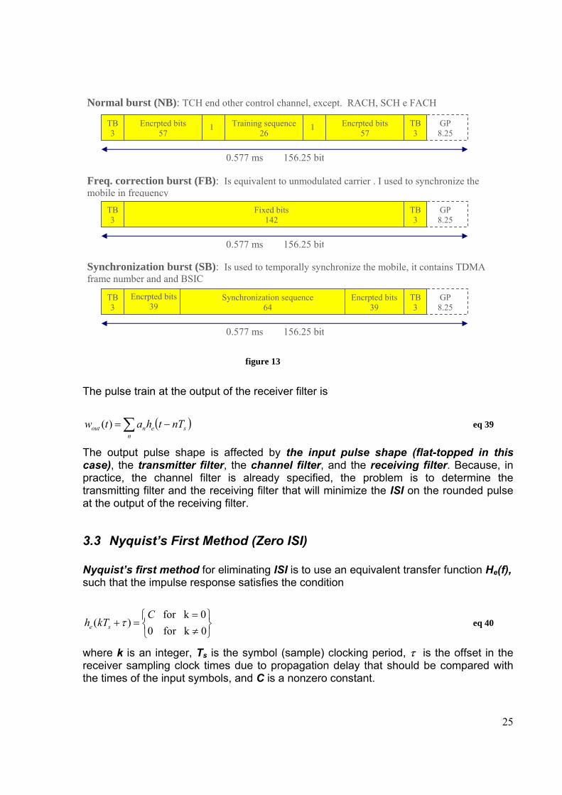
25
figure 13
The pulse train at the output of the receiver filter is
( ) )( ∑ −=n
senout nTthatw eq 39
The output pulse shape is affected by the input pulse shape (flat-topped in this case), the transmitter filter, the channel filter, and the receiving filter. Because, in practice, the channel filter is already specified, the problem is to determine the transmitting filter and the receiving filter that will minimize the ISI on the rounded pulse at the output of the receiving filter.
3.3 Nyquist’s First Method (Zero ISI) Nyquist’s first method for eliminating ISI is to use an equivalent transfer function He(f), such that the impulse response satisfies the condition
⎭⎬⎫
⎩⎨⎧
≠=
=+0kfor 00kfor
)(C
kTh se τ eq 40
where k is an integer, Ts is the symbol (sample) clocking period, τ is the offset in the receiver sampling clock times due to propagation delay that should be compared with the times of the input symbols, and C is a nonzero constant.
Encrpted bits 57
TB 3
Training sequence 26
1 Encrpted bits 57
1 TB 3
GP 8.25
0.577 ms 156.25 bit
Normal burst (NB): TCH end other control channel, except. RACH, SCH e FACH
Fixed bits 142
TB 3
TB 3
GP 8.25
0.577 ms 156.25 bit
Freq. correction burst (FB): Is equivalent to unmodulated carrier . I used to synchronize the mobile in frequency
Synchronization burst (SB): Is used to temporally synchronize the mobile, it contains TDMA frame number and and BSIC
0.577 ms 156.25 bit
TB 3
Synchronization sequence 64
Encrpted bits 39
TB 3
GP 8.25
Encrpted bits 39

26
That is, for a single flat-top pulse of level a at the input to the transmitting filter at t=0, the received pulse would be a⋅he(t) and it would have a value of a⋅C at t=τ (i.e. for K=0) but it would not cause interference at any other sampling time because he(kTs+τ)=0 when k≠0.
figure 14
figure 15
Improper filtering with ISI
1 1 0 0
Input weaveform, win(t)
Individual Nyquist filter pulse response is 0 in KTs
NO ISI
t
Tss
Ts 2Ts 3Ts
1 0 0
t
0 0
t0
Input weaveform, win(t)
1 1 1
t
0 0
t0
Sampling points (trasmitter clock)
tt0
Sampling points (receiver clock)
tt0
Sampling points (receiver clock)
Individual Nyquist filter pulse response is 0 in KTs
tt0
Ts
s
tt0
Received waveform, wout(t) (sum of filter pulse responses)
No Intersymbol interference Ts
Improper filtering with ISI
27
2
2DBDB =+−=−
freq
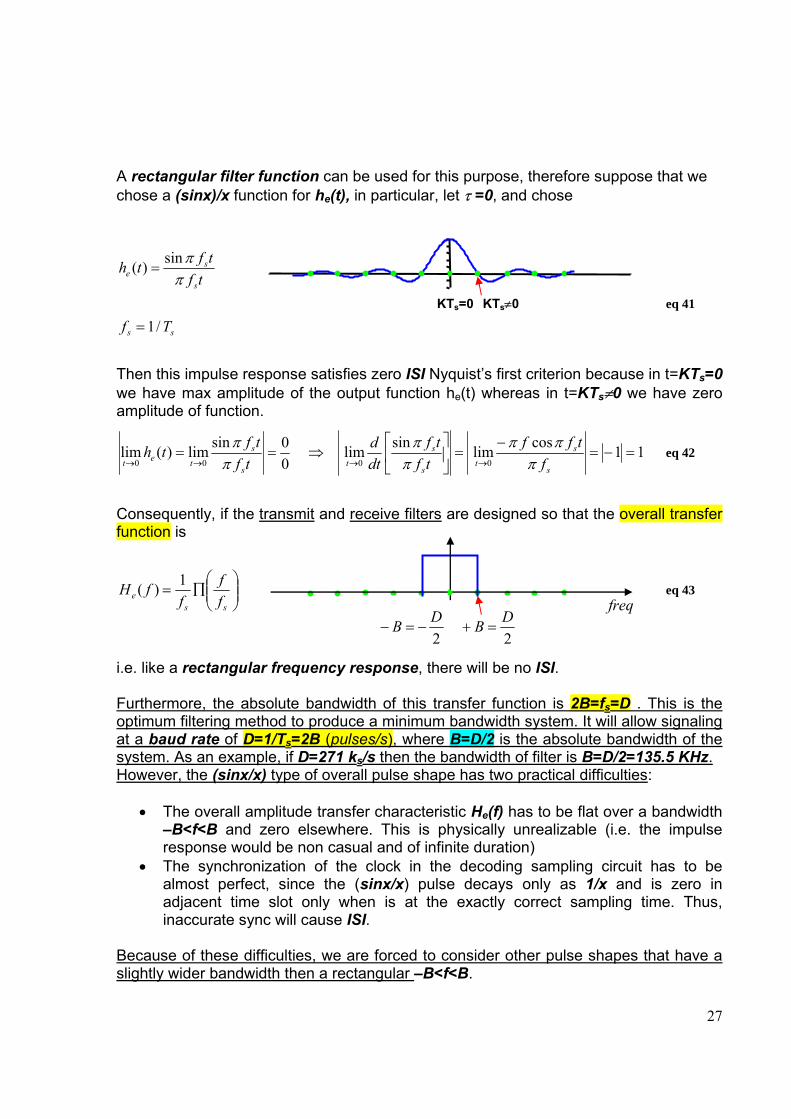
A rectangular filter function can be used for this purpose, therefore suppose that we chose a (sinx)/x function for he(t), in particular, let τ =0, and chose
ss
s
se
Tf
tftfth
/1
sin)(
=
=ππ
KTs=0 KTs≠0 eq 41
Then this impulse response satisfies zero ISI Nyquist’s first criterion because in t=KTs=0 we have max amplitude of the output function he(t) whereas in t=KTs≠0 we have zero amplitude of function.
11coslim sinlim 00sinlim)(lim
0000=−=
−=⎥
⎦
⎤⎢⎣
⎡⇒==
→→→→s
s
ts
s
ts
s
tet ftff
tftf
dtd
tftfth
πππ
ππ
ππ
eq 42
Consequently, if the transmit and receive filters are designed so that the overall transfer function is
⎟⎟⎠
⎞⎜⎜⎝
⎛∏=
sse f
ff
fH 1)( eq 43
i.e. like a rectangular frequency response, there will be no ISI. Furthermore, the absolute bandwidth of this transfer function is 2B=fs=D . This is the optimum filtering method to produce a minimum bandwidth system. It will allow signaling at a baud rate of D=1/Ts=2B (pulses/s), where B=D/2 is the absolute bandwidth of the system. As an example, if D=271 ks/s then the bandwidth of filter is B=D/2=135.5 KHz. However, the (sinx/x) type of overall pulse shape has two practical difficulties:
• The overall amplitude transfer characteristic He(f) has to be flat over a bandwidth –B<f<B and zero elsewhere. This is physically unrealizable (i.e. the impulse response would be non casual and of infinite duration)
• The synchronization of the clock in the decoding sampling circuit has to be almost perfect, since the (sinx/x) pulse decays only as 1/x and is zero in adjacent time slot only when is at the exactly correct sampling time. Thus, inaccurate sync will cause ISI.
Because of these difficulties, we are forced to consider other pulse shapes that have a slightly wider bandwidth then a rectangular –B<f<B.
28
The idea is to find pulse shapes that go through zero at adjacent sampling points and yet have an envelope that decays much faster than 1/x so that clock jitter in the sampling times KTs≠0 does not cause appreciable ISI. One solution for the equivalent transfer function, which has many desirable future, is the raised cosine-rolloff Nyquist filter.
3.4 Raised Cosine-Rolloff Nyquist Filtering DEFINITION: the raised cosine-rolloff Nyquist filter has the transfer function:
( )
⎪⎪⎭
⎪⎪⎬
⎫
⎪⎪⎩
⎪⎪⎨
⎧
>
<<⎪⎭
⎪⎬⎫
⎪⎩
⎪⎨⎧
⎥⎦
⎤⎢⎣
⎡ −+
<
=∆
Bf
Bfff
ffff
fHe
,0
,2
cos121
,1
)( 11
1
π eq 44
Where B is the absolute bandwidth and the parameters f∆ and f1 are
∆
∆
−=
−=
fff
fBf
01
0
eq 45
f0 is the 6-dB Raised Cosine filter bandwidth
00
rf fffr ∆ =⇒= ∆ eq 46
Where r is the rolloff factor of the filter. Consequently
)1(
)1(
00001
0000
rfrfffff
rfrffffB
−=−=−=
+=+=+=
∆
∆
eq 47
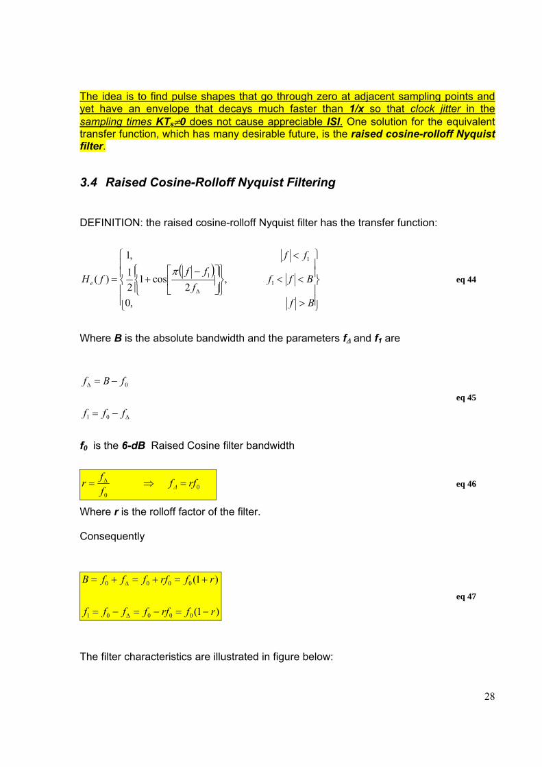
The filter characteristics are illustrated in figure below:
29
figure 16
For several value of the rolloff factor r the corresponding required signaling transmission bandwidth B are:
figure 17
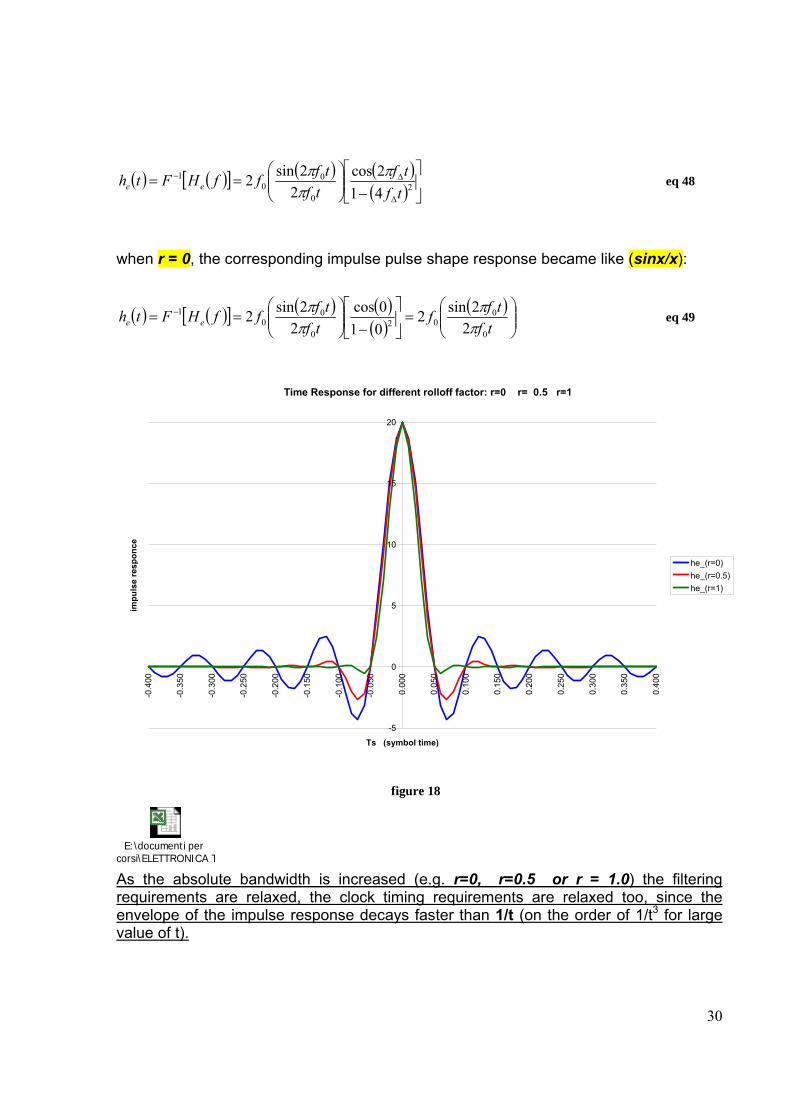
For rolloff factors r=0 we have f∆=0 and we obtain the minimum-bandwidth required case, where f0=B. The corresponding impulse shape response is
r0=0, min bandwidth
r1=0.5
0.5
1.0
Freq.
He(f)
r2=1
f0=fB
f∆ f∆
f0 B -B f1 -f1 -f0
0.5
1.0
Freq.
He(f)
6-db bandwidth
30
( ) ( )[ ] ( ) ( )( ) ⎥⎦
⎤⎢⎣
⎡
−⎟⎟⎠
⎞⎜⎜⎝
⎛==
∆
∆−2
0
00
1
412cos
22sin2
tftf
tftfffHFth ee
πππ
eq 48
when r = 0, the corresponding impulse pulse shape response became like (sinx/x):
( ) ( )[ ] ( ) ( )( )
( )⎟⎟⎠
⎞⎜⎜⎝
⎛=⎥
⎦
⎤⎢⎣
⎡
−⎟⎟⎠
⎞⎜⎜⎝
⎛== −
tftff
tftfffHFth ee
0
002
0
00
1
22sin2
010cos
22sin2
ππ
ππ
eq 49
Time Response for different rolloff factor: r=0 r= 0.5 r=1
-5
0
5
10
15
20
-0.4
00
-0.3
50
-0.3
00
-0.2
50
-0.2
00
-0.1
50
-0.1
00
-0.0
50
0.00
0
0.05
0
0.10
0
0.15
0
0.20
0
0.25
0
0.30
0
0.35
0
0.40
0
Ts (symbol time)
impu
lse
resp
once
he_(r=0)he_(r=0.5)he_(r=1)
figure 18
E:\documenti per corsi\ELETTRONICA T As the absolute bandwidth is increased (e.g. r=0, r=0.5 or r = 1.0) the filtering requirements are relaxed, the clock timing requirements are relaxed too, since the envelope of the impulse response decays faster than 1/t (on the order of 1/t3 for large value of t).
31
Let us now develop a formula which gives the baud rate that the raised cosine-rolloff system can support without ISI. From figure above, the zeros in the system impulse response occur at t =n/2f0 where n≠0. Therefore, data pulses may be inserted at each of these zero points without causing ISI. That is, referring to
⎭⎬⎫
⎩⎨⎧
≠=
=+0kfor 00kfor
)(C
kTh se τ eq 50
with τ =0, we see that the raised cosine-rolloff filter, satisfies Nyquist’s first criterion (for the absence of ISI) if the symbol clock period is equal to Ts=1/(2f0). The corresponding baud rate is
( )2
/ 2100
DfsSymbolfT
Ds
=⇒==
That is, the 6-dB bandwidth of the raised cosine-rolloff filter, f0, is designed to be half the symbol (baud) rate.
12 2
D
2
2
22
2
2 0
0
0
rB DDBr D
DBD
DB
D
DB
ffB
ffr
+=⇒−=⋅⇒
⇒−
=
−
=−
=−
== ∆
eq 51
where B is the absolute bandwidth of the system and r is the system rolloff factor.
( )rDB += 12
eq 52
The greater r the grater B, and as a function of B and r we can aspect a maximum value of symbol rate D. Comparing to first criteria where B=D/2 now the bandwidth is increased when r≠0
32
4 BANDPASS SIGNALING
4.1 COMPLEX ENVELOPE RAPPRESTNATION OF BANDPASS WAVEFORMS
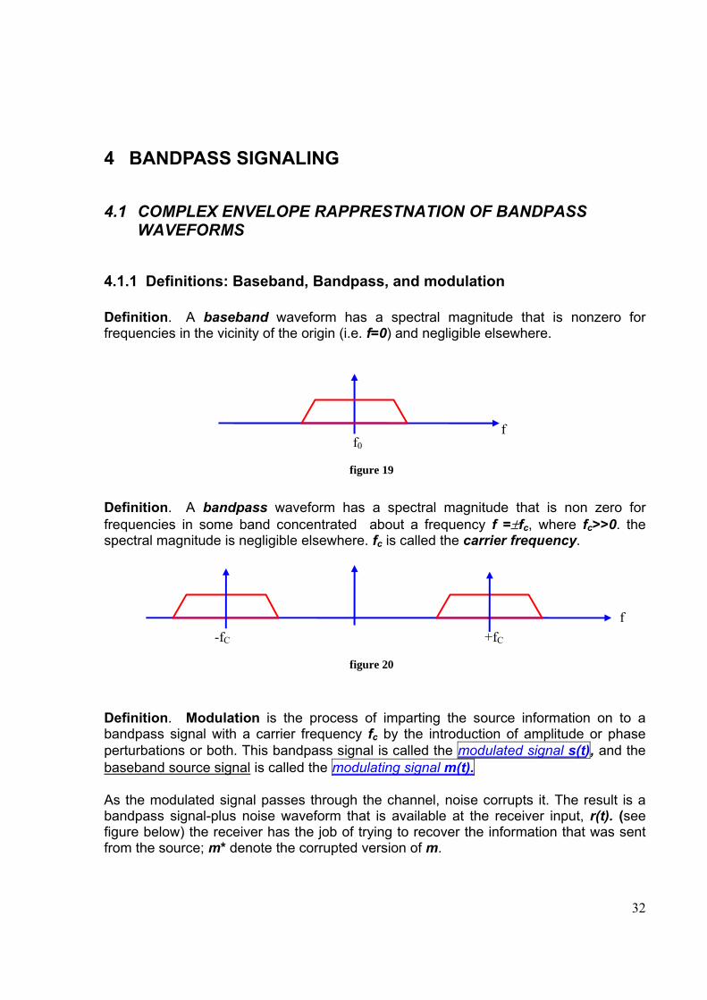
4.1.1 Definitions: Baseband, Bandpass, and modulation Definition. A baseband waveform has a spectral magnitude that is nonzero for frequencies in the vicinity of the origin (i.e. f=0) and negligible elsewhere.
figure 19
Definition. A bandpass waveform has a spectral magnitude that is non zero for frequencies in some band concentrated about a frequency f =±fc, where fc>>0. the spectral magnitude is negligible elsewhere. fc is called the carrier frequency.
figure 20
Definition. Modulation is the process of imparting the source information on to a bandpass signal with a carrier frequency fc by the introduction of amplitude or phase perturbations or both. This bandpass signal is called the modulated signal s(t), and the baseband source signal is called the modulating signal m(t). As the modulated signal passes through the channel, noise corrupts it. The result is a bandpass signal-plus noise waveform that is available at the receiver input, r(t). (see figure below) the receiver has the job of trying to recover the information that was sent from the source; m* denote the corrupted version of m.
+fC -fC
f
f0 f
33
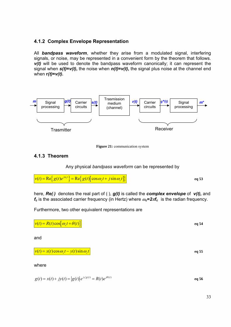
4.1.2 Complex Envelope Representation All bandpass waveform, whether they arise from a modulated signal, interfering signals, or noise, may be represented in a convenient form by the theorem that follows. v(t) will be used to denote the bandpass waveform canonically; it can represent the signal when s(t)=v(t), the noise when n(t)=v(t), the signal plus noise at the channel end when r(t)=v(t).
Figure 21: communication system
4.1.3 Theorem
Any physical bandpass waveform can be represented by
{ } [ ]{ }( ) Re ( ) Re ( ) cos sincj tc cv t g t e g t t j tω ω ω= = + eq 53
here, Re(⋅) denotes the real part of (⋅), g(t) is called the complex envelope of v(t), and fc is the associated carrier frequency (in Hertz) where ωc=2πfc is the radian frequency. Furthermore, two other equivalent representations are
[ ]( ) ( ) cos ( )cv t R t t tω θ= + eq 54
and
( ) ( ) cos ( )sinc cv t x t t y t tω ω= − eq 55
where
( ) ( )( ) ( ) ( ) ( ) ( )j g t j tg t x t jy t g t e R t e θ∠= + = = eq 56
Signal processing
Carrier circuits
Trasmission medium
(channel) Carrier circuits
Signal processing
m g(t) s(t) r(t) g*(t) m*
Trasmitter Receiver
34
{ }( ) Re ( ) ( ) cos ( )x t g t R t tθ= = eq 57
{ }( ) Im ( ) ( )sin ( )y t g t R t tθ= = eq 58
2 2( ) ( ) ( ) ( )R t g t x t y t= + eq 59
and
1 ( )( ) ( ) tan( )
y tt g tx t
θ − ⎛ ⎞∠ = ⎜ ⎟
⎝ ⎠ eq 60
Consequently we obtain:
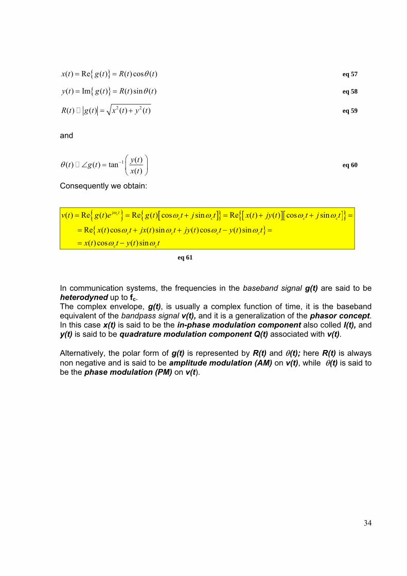
{ } [ ]{ } [ ][ ]{ }{ }
( ) Re ( ) Re ( ) cos sin Re ( ) ( ) cos sin
Re ( )cos ( )sin ( )cos ( )sin ( ) cos ( )sin
cj tc c c c
c c c c
c c
v t g t e g t t j t x t jy t t j t
x t t jx t t jy t t y t tx t t y t t
ω ω ω ω ω
ω ω ω ω
ω ω
= = + = + + =
= + + − =
= −
eq 61
In communication systems, the frequencies in the baseband signal g(t) are said to be heterodyned up to fc. The complex envelope, g(t), is usually a complex function of time, it is the baseband equivalent of the bandpass signal v(t), and it is a generalization of the phasor concept. In this case x(t) is said to be the in-phase modulation component also colled I(t), and y(t) is said to be quadrature modulation component Q(t) associated with v(t). Alternatively, the polar form of g(t) is represented by R(t) and θ(t); here R(t) is always non negative and is said to be amplitude modulation (AM) on v(t), while θ(t) is said to be the phase modulation (PM) on v(t).
35
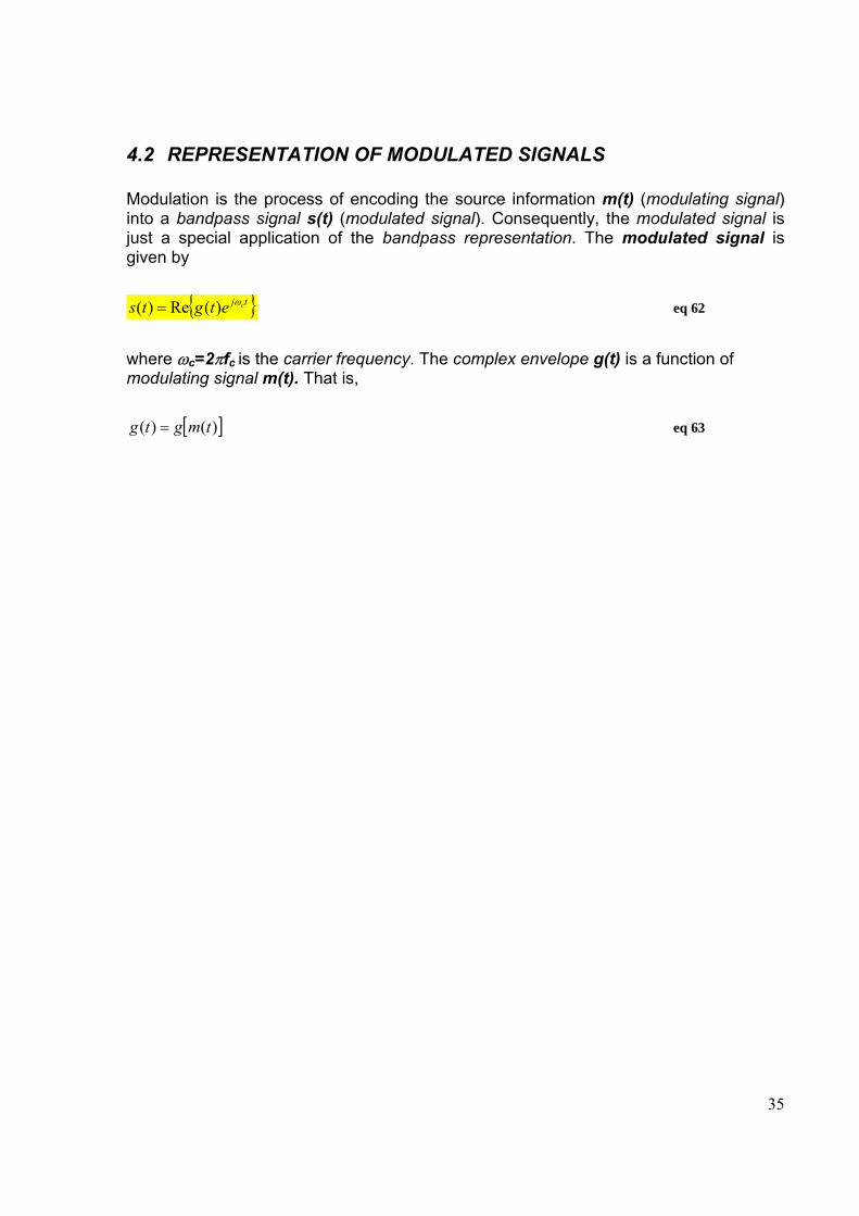
4.2 REPRESENTATION OF MODULATED SIGNALS Modulation is the process of encoding the source information m(t) (modulating signal) into a bandpass signal s(t) (modulated signal). Consequently, the modulated signal is just a special application of the bandpass representation. The modulated signal is given by
{ }tj cetgts ω)(Re)( = eq 62
where ωc=2πfc is the carrier frequency. The complex envelope g(t) is a function of modulating signal m(t). That is,
[ ])()( tmgtg = eq 63
36
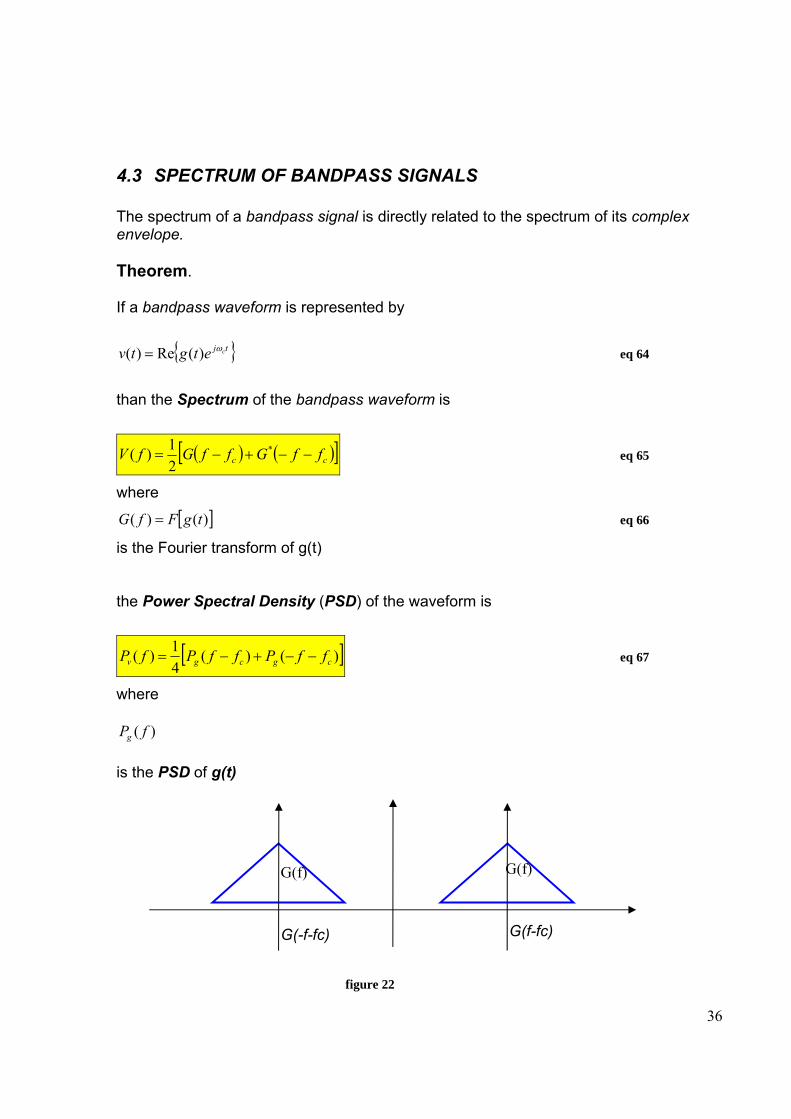
4.3 SPECTRUM OF BANDPASS SIGNALS The spectrum of a bandpass signal is directly related to the spectrum of its complex envelope. Theorem. If a bandpass waveform is represented by
{ }tj cetgtv ω)(Re)( = eq 64
than the Spectrum of the bandpass waveform is
( ) ( )[ ]cc ffGffGfV −−+−= *
21)( eq 65
where
[ ])()( tgFfG = eq 66
is the Fourier transform of g(t) the Power Spectral Density (PSD) of the waveform is
[ ])()(41)( cgcgv ffPffPfP −−+−= eq 67
where
)( fPg is the PSD of g(t)
figure 22
G(-f-fc) G(f-fc)
G(f) G(f)
37
5 AM, FM, PM MODULATED SYSETMS
5.1 Definitions
Amplitude Modulation (AM) is a system where the frequency of a carrier wave is held constant while the amplitude is varied in sympathy with the voltage of the modulating signal.
Frequency Modulation (FM) is a system where the amplitude of a carrier wave is held constant while the frequency is varied in sympathy with the voltage of the modulating signal.
Phase Modulation (PM) is a similar system where the phase of the carrier wave is varied in sympathy with the voltage of the modulating signal, and as in frequency modulation, the amplitude of a carrier is held constant.
Phase is the position of a rotating vector or phasor.
Angular Velocity is the rate of change of phase (usually expressed in radians per second).
The Radian is a unit of angular displacement (as is degrees), there are 2*π radians in a full circle (or 360°), so a radian is approximately 57°.
Frequency is a measure of the number of repetitions of a periodic waveform in unit time (1 second). Frequency of a carrier wave is related to Angular Velocity, there are 2*π radians in each cycle of a carrier wave, so the Angular Velocity is 2*π * frequency.
Pi is a numeric constant, it's value is approximately 3.1411592654. (You can approximate it by using 22/7 - the error is less than 0.05%).
5.2 AMPLITUDE MODULATION The complex envelope of an AM signal is given by
[ ]( ) 1 ( )cg t A m t= + eq 68
Where the constant Ac, has been included to specify the power level and m(t) is the modulating signal (which may be analog or digital). These equations reduce to the following representation for AM signal:
38
[ ] [ ][ ]ttmjAttmA
etmAeTgts
cccc
tjc
tj cc
ωω
ωω
sin))(1(cos))(1(Re ))(1(Re)(Re)(+++=
=+== eq 69
[ ]( ) 1 ( ) cosc cs t A m t tω= + eq 70
For convenience, it is assumed that the modulating signal m(t) is a sinusoid. The modulating signal corresponds to the in-phase component x(t) of the complex envelope; it also correspond to the real envelope ( )g t when m(t)≥-1 (the usual case).
If ( ) cos( )mm t m tω= eq 71
Then recalling that ( ) ( )[ ]βαβαβα −++= coscos21coscos we have
[ ] [ ]
( ) ( )
( ) 1 ( ) cos 1 cos cos cos cos cos1 1 cos cos cos2 2
c c c m c c c c m c
c c c c m c c m
s t A m t t A m t t A t A m t t
A t A m t A m t
ω ω ω ω ω ω
ω ω ω ω ω
= + = + = + =
= + + + − eq 72
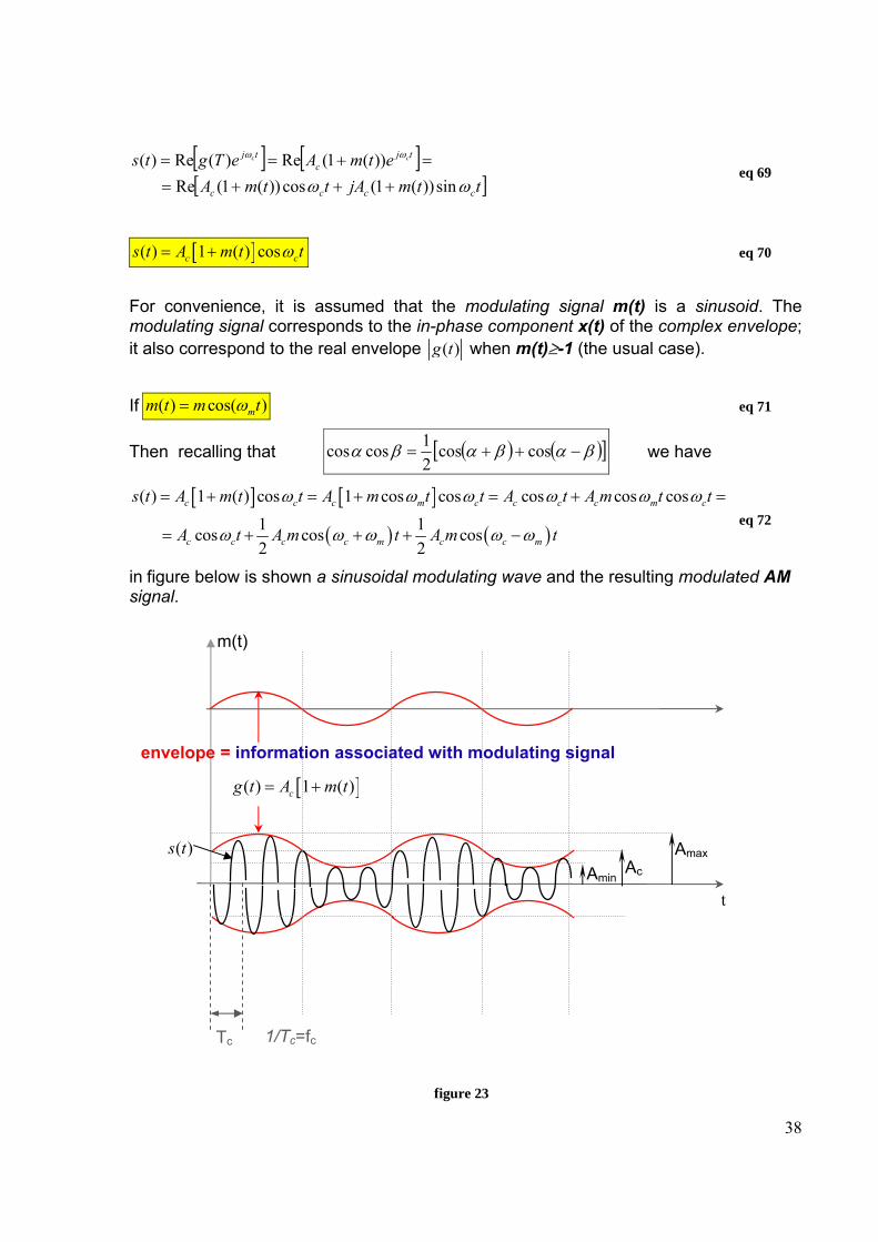
in figure below is shown a sinusoidal modulating wave and the resulting modulated AM signal.
figure 23
1/Tc=fc Tc
[ ]( ) 1 ( )cg t A m t= +
( )s t Amin
envelope = information associated with modulating signal
Ac Amax
t
m(t)
39
The overall modulation percentage is:
[ ] [ ]max min max ( ) -min ( )A -A%modulation= 100 1002Ac 2Ac
m t m t= eq 73
5.2.1 Normalized AM average power The normalized average power of an AM signal is:
[ ] )(21)(
21)(2)(1
21)(1
21
)(21)(
22222222
22
tmAtmAAtmtmAtmA
tgts
ccccc ++=++=+=
== eq 74
If modulation m(t) contains no dc level, then 0)( =tm and the normalized power of an AM signal is
The voltage magnitude spectrum of the AM signal is given by:
( ) ( ) ( ) ( )[ ]ccccc ffMffffMffAfS ++++−+−= δδ
2)( eq 76
)(21
21)( 2222 tmAAts cc += eq
discrete carrier power
sideband power
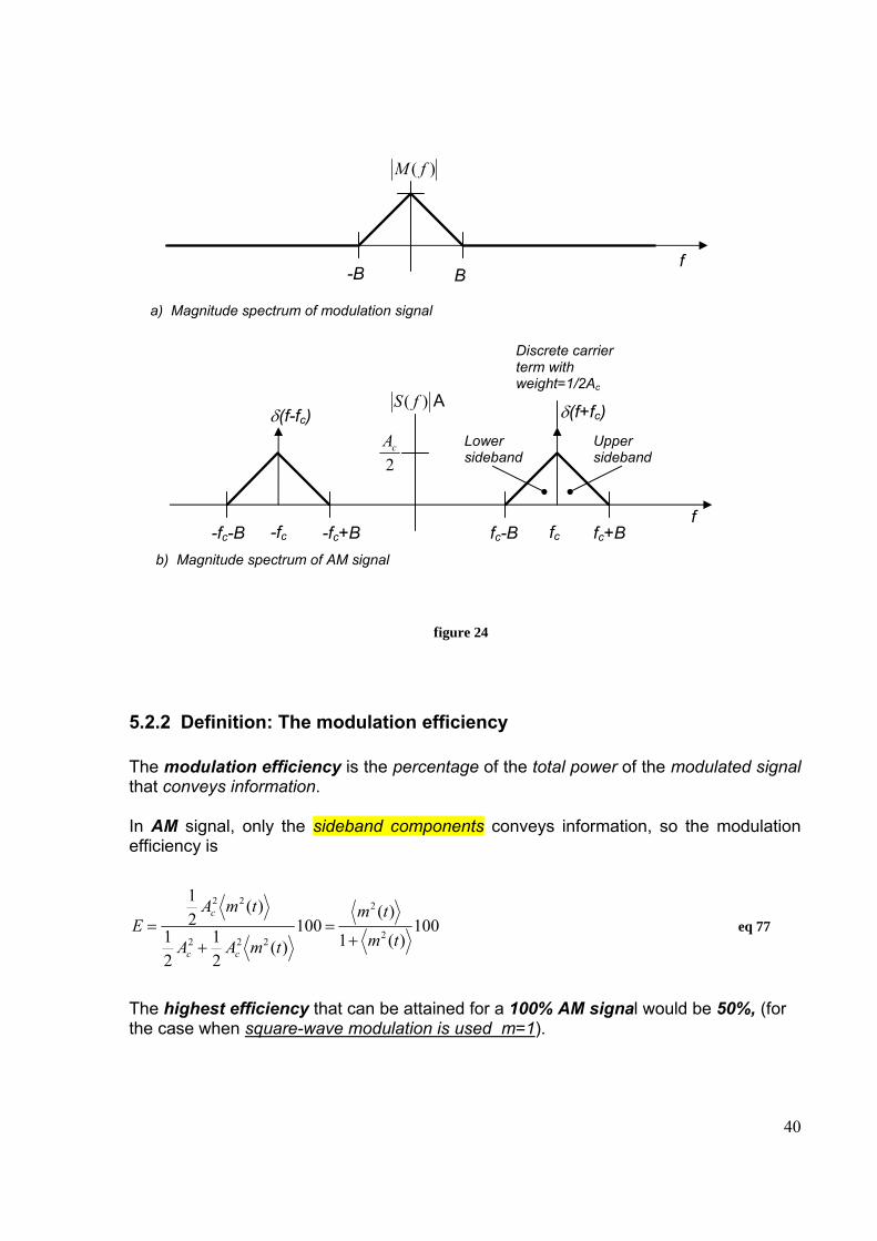
40
figure 24
5.2.2 Definition: The modulation efficiency The modulation efficiency is the percentage of the total power of the modulated signal that conveys information. In AM signal, only the sideband components conveys information, so the modulation efficiency is
100)(1
)(100
)(21
21
)(21
2
2
222
22
tm
tm
tmAA
tmAE
cc
c
+=
+= eq 77
The highest efficiency that can be attained for a 100% AM signal would be 50%, (for the case when square-wave modulation is used m=1).
)( fS A
2cA
fc-B fc+B fc -fc-B -fc+B -fc
-B
)( fM
Upper sideband
Lower sideband
Discrete carrier term with weight=1/2Ac
a) Magnitude spectrum of modulation signal
f
f
b) Magnitude spectrum of AM signal
B
δ(f-fc) δ(f+fc)
41
6 PHASE MODULATION AND FREQUENCY MODULATION
6.1 Representation of PM and FM Signals Phase Modulation (PM) and Frequency modulation (FM) are special cases of angle-modulated signaling. In this kind of signaling the complex envelope is
)()( tjceAtg θ= eq 78
here θ(t) is a linear function of the modulating signal m(t), while g(t) is a non linear function of the modulation. The resulting angle-modulated signal is:
{ } { } [ ]{ } [ ])(cosReRe)(Re)( )()( ttAeAeeAetgts ccttj
ctjtj
ctj ccc θωωθωθω +==== + eq 79
The relation between phase θ(t) and the instantaneous frequency fi is:
2)( )(21
∫∞−
=⇒=t
ii dtftdt
tdf πθθπ
eq 80
1. for PM, the phase is directly proportional to the modulating signal m(t);
)()( tmDt p=θ eq 81
Where the proportionally constant Dp is the phase sensitivity(phase deviation constant) of the phase modulator, having units of radians per volt [assuming that m(t) is a voltage waveform].
2. For FM, the phase is proportional to the integral of m(t), so that
σσθ dmDtt
f ∫∞−
= )()( eq 82
where the frequency deviation constant Df, has units of radians/volt-second.
42
We can develop an example for a PM first and FM later. suppose
tAtm mm ωcos)( = eq 83
• in the PM case we have
ttADtmDt mpmmpp ωβωθ coscos)()( === eq 84
Where
mpp AD=β is the phase modulation index • in the FM case we have
ttDAdADdmDt mfmfm
t
mmf
t
f ωβωω
σσωσσθ sinsin1cos)()( ==== ∫∫∞−∞−
eq 85
Where
mfmf DAω
β 1= is the frequency modulation index
The complex envelope is:
tjc
tjc
mfeAeAtg ωβθ sin)()( == eq 86
Therefore the modulated bandpass signal is:
{ }{ } [ ]{ } [ ]
⎥⎦
⎤⎢⎣
⎡+=⎥
⎦
⎤⎢⎣
⎡+=
=+===
==
∫∫∞−∞−
+
t
mm
mfcc
t
mfcc
cmfcttj
ctjtj
c
tj
tAD
tAttA
ttAeAeeA
etgtscmfcmf
c
ωω
ωωβω
ωωβωωβωωβ
ω
coscoscoscos
sincosReRe
)(Re)(sinsin
eq 87
43
the last term: [ ]tt mfc ωβω sincos + can be studied by Bessels function
figure 25
Definition. If a bandpass signal is represented by
[ ])(cos)()(cos)()( tttRttRts c θωψ +== eq 88
then the instantaneous frequency (Hertz) of s(t) is [Boashash, 1992]
[ ]
dttdf
dttd
dtttd
dttdttf
cc
cii
)(21)(
21
21
)(21)(
21)(
21)(
θπ
θπ
ωπ
θωπ
ψπ
ωπ
+=+=
=⎥⎦⎤
⎢⎣⎡ +
=⎥⎦⎤
⎢⎣⎡==
eq 89
Therefore using σσθ dmDtt
f ∫∞−
= )()(
)(21
)(
21)(
21)( tmDf
dt
dmDdf
dttdftf fc
t
f
cci π
σσ
πθ
π+=
⎥⎦
⎤⎢⎣
⎡
+=+=∫∞− eq 90
44
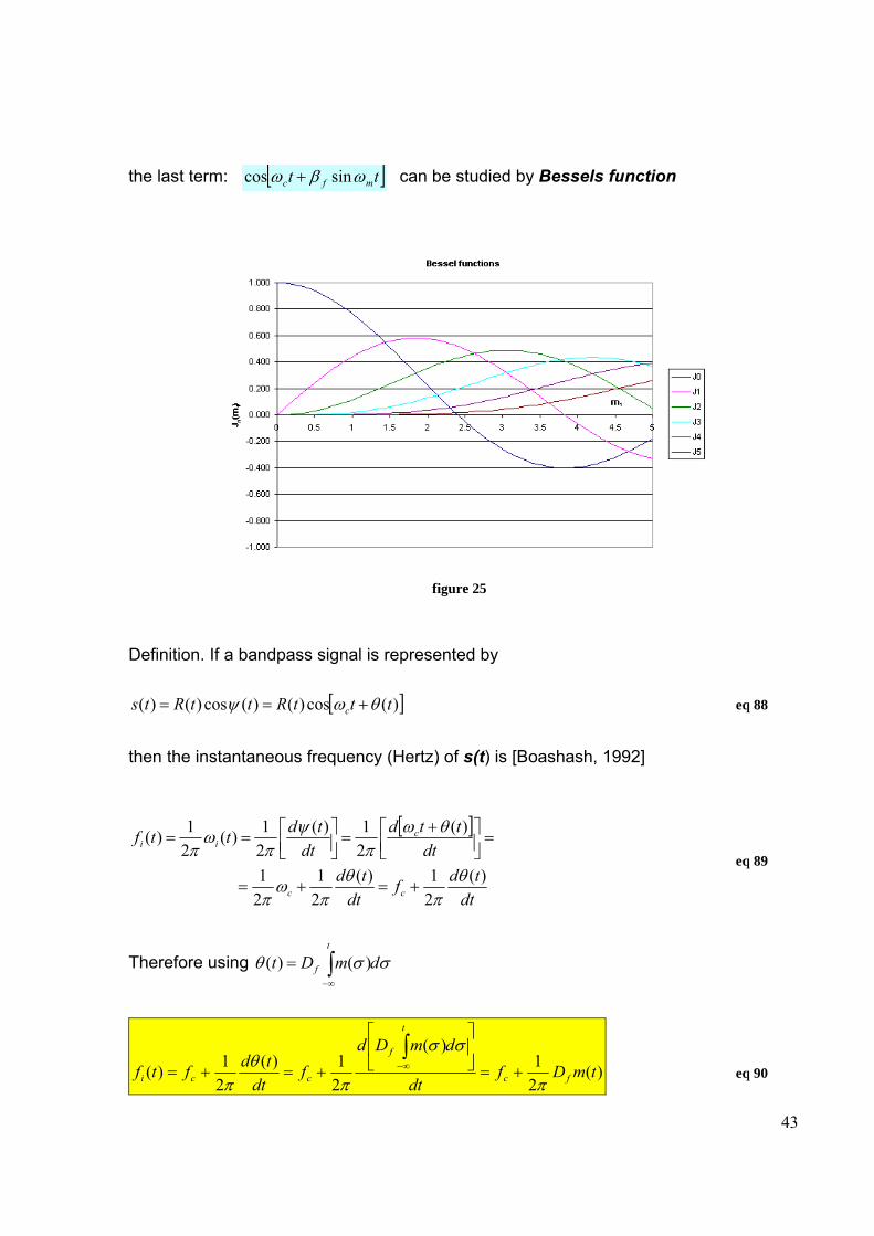
Of course, this is the reason for calling this type of signaling frequency modulation—the instantaneous frequency varies about the assigned carrier frequency fc, in a manner that is directly proportional to the modulating signal m(t).
figure 26
figure above show how the instantaneous frequency varies when a sinusoidal modulation (for illustrative purposes ) is used. The frequency deviation from the carrier frequency is
dttdftftf cid)(
21)()( θπ
=−= eq 91
and the peak frequency deviation is
[ ] ⎥⎦⎤
⎢⎣⎡==∆
dttdtff d)(
21max)(max θπ
eq 92
fc+∆f
fc-∆f
fc
fi(t)---istantaneous frequency of the corresponding FM signal
m(t)---sinusoidal modulating signal
s(t)---correspondign FM signal
vp
Ac
s(t)---has constant amplitude
45
note that ∆f is a non negative number. In some applications, such as unipolar digital modulation, the peak to peak deviation is used:
⎥⎦⎤
⎢⎣⎡−⎥⎦
⎤⎢⎣⎡=∆
dttd
dttdf pp
)(21min)(
21max θ
πθ
π eq 93
For FM signaling, the peak frequency deviation is related to the peak modulating voltage by:
[ ] [ ] pfffd VDtmDtmDdt
tdtffπππ
θπ 2
1)(max21)(
21max)(
21max)(max ==⎥⎦
⎤⎢⎣⎡=⎥⎦
⎤⎢⎣⎡==∆ eq 94
An increase in the amplitude of the modulation signal Vp will increase ∆f. This in turn will increase the bandwidth of the FM signal, but will not affect the average power level of the FM signal, which is AC
2/2. As Vp is increased, spectral components will appear farther and farther away from the carrier frequency, and the spectral components near the carrier frequency will decrease in magnitude, since the total power in the signal remains constant. This situation is distinctly different from AM signaling, where the level of the modulation affects the power in the AM signal, but does not affect its bandwidth. In a similar way, the peak phase deviation may be defined by:
[ ])(max tθθ =∆ eq 95
which for PM, is related to the peak modulation voltage by
[ ])(max tmDVD ppp ==∆θ eq 96
6.1.1 Definition for peak phase deviation and peak frequency deviaton.
• The phase modulation index is given by
θβ ∆=p eq 97
where ∆θ is the peak phase deviation.
• The frequency modulation index is given by:
46
BF
f∆
=β eq 98
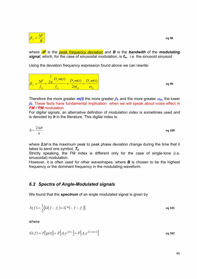
where ∆F is the peak frequency deviation and B is the bandwith of the modulating signal, which, for the case of sinusoidal modulation, is fm, i.e the sinusoid sinusoid. Using the deviation frequency expression found above we can rewrite:
m
f
m
f
m
f
mf
tmDf
tmDf
tmD
fF
ωππβ
)(2
)()(21
===∆
= eq 99
Therefore the more greater m(t) the more greater βf, and the more greater ωm, the lower βf. These facts have fundamental implication when we will speak about noise effect in FM / PM modulation. For digital signals, an alternative definition of modulation index is sometimes used and is denoted by h in the literature. This digital index is:
πθ∆
=2h eq 100
where 2∆θ is the maximum peak to peak phase deviation change during the time that it takes to send one symbol, Ts. Strictly speaking, the FM index is different only for the case of single-tone (i.e. sinusoidal) modulation. However, it is often used for other waveshapes, where B is chosen to be the highest frequency or the dominant frequency in the modulating waveform.
6.2 Spectra of Angle-Modulated signals We found that the spectrum of an angle modulated signal is given by
( ) ( )[ ]cc ffGffGfS −−+−= *21)( eq 101
where
[ ] [ ] [ ][ ])(()()()( tmfjc
tjc eAFeAFtgFfG === θ eq 102
47
Since g(t) is a non linear function of m(t) a general formula relating G(f) cannot be obtained, that is G(f) must be evaluated case by case basis for the particular modulating waveshape of interest, furthermore superposition does not hold, and the FM spectrum for the sum of two modulating waveshapes is not the same as summing the FM spectra that were obtained when the individual waveshapes were used. The evaluation into a closed form is not easy, one often has to use a numerical techniques to approximate the Fourier transform integral. An example for the case of sinusoidal waveshape will now be worked out.
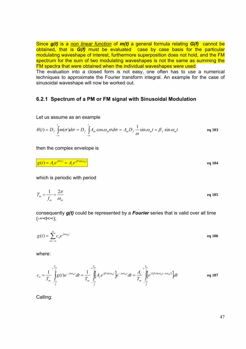
6.2.1 Spectrum of a PM or FM signal with Sinusoidal Modulation Let us assume as an example
ttDAdADdmDt mfmfm
t
mmf
t
f ωβωω
σσωσσθ sinsin1cos)()( ==== ∫∫∞−∞−
eq 103
then the complex envelope is
tjc
tjc
meAeAtg ωβθ sin)()( == eq 104
which is periodic with period
mmm f
Tωπ21
== eq 105
consequently g(t) could be represented by a Fourier series that is valid over all time (-∞<t<∞);
∑∞
−∞=
=n
tjnn
mectg ω)( eq 106
where:
[ ] ( )[ ]dteTAdteeA
Tdtetg
Tc
m
m
mmm
m
m
mm
m
m
T
T
tntj
m
ctjn
T
T
tjc
m
tjn
T
Tmn ∫∫∫
+
−
−−
+
−
−
+
−
===2
2
sin2
2
sin2
2
1)(1 ωωβωωβω eq 107
Calling:
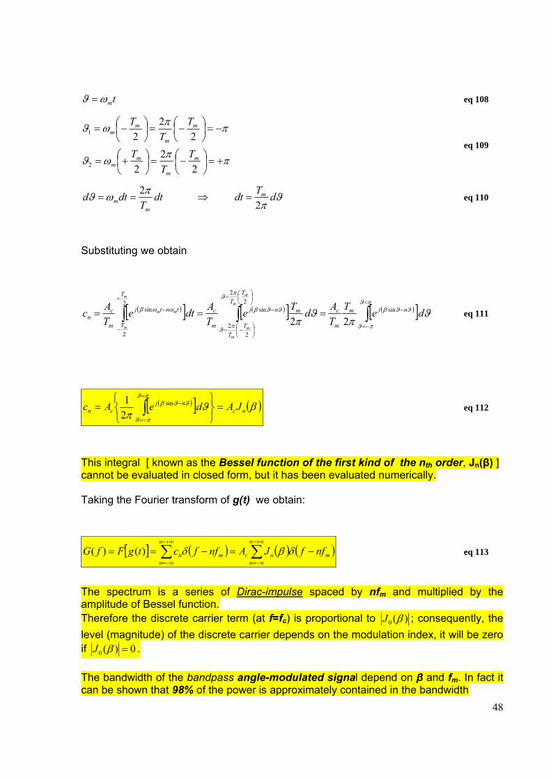
48
tmωϑ = eq 108
ππωϑ
ππωϑ
+=⎟⎠⎞
⎜⎝⎛−=⎟
⎠⎞
⎜⎝⎛+=
−=⎟⎠⎞
⎜⎝⎛−=⎟
⎠⎞
⎜⎝⎛−=
22
2
22
2
2
1
m
m
mm
m
m
mm
TT
T
TT
T
eq 109
ϑπ
πωϑ dTdtdtT
dtd m
mm 2
2=⇒== eq 110
Substituting we obtain
( )[ ] ( )[ ] ( )[ ] ϑπ
ϑπ
πϑ
πϑ
ϑϑβ
πϑ
πϑ
ϑϑβωωβ deTTAdTe
TAdte
TAc njm
m
cm
TT
TT
nj
m
c
T
T
tntj
m
cn
m
m
m
m
m
m
mm ∫∫∫=
−=
−
⎟⎠⎞
⎜⎝⎛=
⎟⎠⎞
⎜⎝⎛ −=
−
+
−
− === sin2
2
22
sin2
2
sin
22 eq 111
( )[ ] ( )βϑπ
πϑ
πϑ
ϑϑβnc
njcn JAdeAc =
⎭⎬⎫
⎩⎨⎧
= ∫=
−=
−sin
21
eq 112
This integral [ known as the Bessel function of the first kind of the nth order, Jn(β) ] cannot be evaluated in closed form, but it has been evaluated numerically. Taking the Fourier transform of g(t) we obtain:
[ ] ( ) ( ) ( )∑∑+∞=
−∞=
+∞=
−∞=
−=−==n
nmnc
n
nmn nffJAnffctgFfG δβδ)()( eq 113
The spectrum is a series of Dirac-impulse spaced by nfm and multiplied by the amplitude of Bessel function. Therefore the discrete carrier term (at f=fc) is proportional to )(0 βJ ; consequently, the level (magnitude) of the discrete carrier depends on the modulation index, it will be zero if 0)(0 =βJ . The bandwidth of the bandpass angle-modulated signal depend on β and fm. In fact it can be shown that 98% of the power is approximately contained in the bandwidth
49
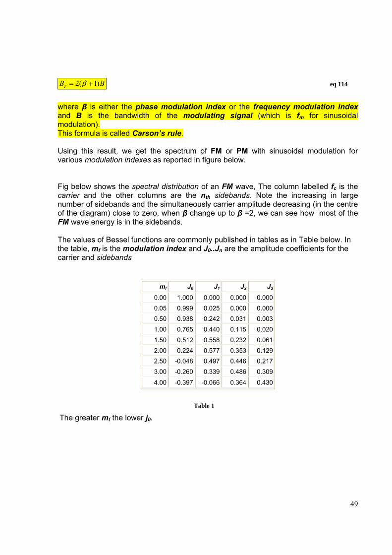
BBT )1(2 += β eq 114
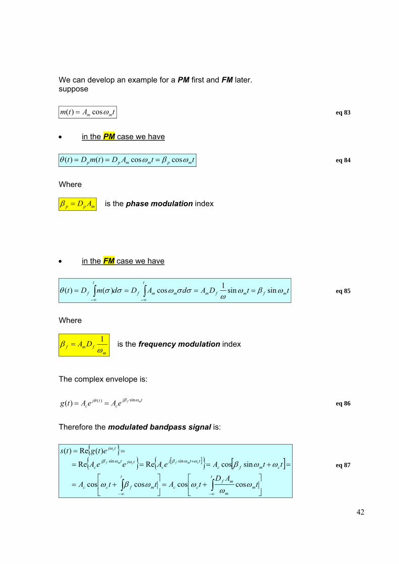
where β is either the phase modulation index or the frequency modulation index and B is the bandwidth of the modulating signal (which is fm for sinusoidal modulation). This formula is called Carson’s rule. Using this result, we get the spectrum of FM or PM with sinusoidal modulation for various modulation indexes as reported in figure below.
Fig below shows the spectral distribution of an FM wave, The column labelled fc is the carrier and the other columns are the nth sidebands. Note the increasing in large number of sidebands and the simultaneously carrier amplitude decreasing (in the centre of the diagram) close to zero, when β change up to β =2, we can see how most of the FM wave energy is in the sidebands.
The values of Bessel functions are commonly published in tables as in Table below. In the table, mf is the modulation index and J0..Jn are the amplitude coefficients for the carrier and sidebands
mf J0 J1 J2 J3
0.00 1.000 0.000 0.000 0.0000.05 0.999 0.025 0.000 0.0000.50 0.938 0.242 0.031 0.0031.00 0.765 0.440 0.115 0.0201.50 0.512 0.558 0.232 0.0612.00 0.224 0.577 0.353 0.1292.50 -0.048 0.497 0.446 0.2173.00 -0.260 0.339 0.486 0.309
4.00 -0.397 -0.066 0.364 0.430
Table 1
The greater mf the lower j0.
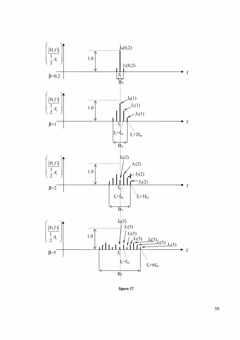
50
figure 27
1.0
J0(0,2)
J1(0,2) ⎟⎟⎟⎟
⎠
⎞
⎜⎜⎜⎜
⎝
⎛
cA
fS
21
)(
f β=0,2
1.0
J0(1) J1(1)
⎟⎟⎟⎟
⎠
⎞
⎜⎜⎜⎜
⎝
⎛
cA
fS
21
)(
f β=1
J2(1)
fc BT
fc
fc+fm
BT
fc+2fm
1.0
J0(2) J1(2)
⎟⎟⎟⎟
⎠
⎞
⎜⎜⎜⎜
⎝
⎛
cA
fS
21
)(
f β=2
J2(2)
fc
fc+fm
BT
fc+3fm
J2(2)
1.0
J0(5) J1(5)
⎟⎟⎟⎟
⎠
⎞
⎜⎜⎜⎜
⎝
⎛
cA
fS
21
)(
f β=5
J2(5)
fc
fc+fm
BT
fc+6fm
J3(5) J4(5) J5(5) J6(5)
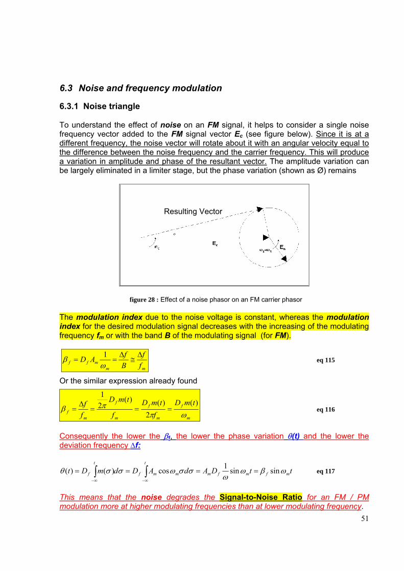
51
6.3 Noise and frequency modulation
6.3.1 Noise triangle
To understand the effect of noise on an FM signal, it helps to consider a single noise frequency vector added to the FM signal vector Ec (see figure below). Since it is at a different frequency, the noise vector will rotate about it with an angular velocity equal to the difference between the noise frequency and the carrier frequency. This will produce a variation in amplitude and phase of the resultant vector. The amplitude variation can be largely eliminated in a limiter stage, but the phase variation (shown as Ø) remains
figure 28 : Effect of a noise phasor on an FM carrier phasor
The modulation index due to the noise voltage is constant, whereas the modulation index for the desired modulation signal decreases with the increasing of the modulating frequency fm or with the band B of the modulating signal (for FM).
mm
mff ff
BfAD ∆≅
∆==
ωβ 1
eq 115
Or the similar expression already found
m
f
m
f
m
f
mf
tmDf
tmDf
tmD
ff
ωππβ
)(2
)()(21
===∆
= eq 116
Consequently the lower the βf, the lower the phase variation θ(t) and the lower the deviation frequency ∆f:
ttDAdADdmDt mfmfm
t
mmf
t
f ωβωω
σσωσσθ sinsin1cos)()( ==== ∫∫∞−∞−
eq 117
This means that the noise degrades the Signal-to-Noise Ratio for an FM / PM modulation more at higher modulating frequencies than at lower modulating frequency.
Resulting Vector
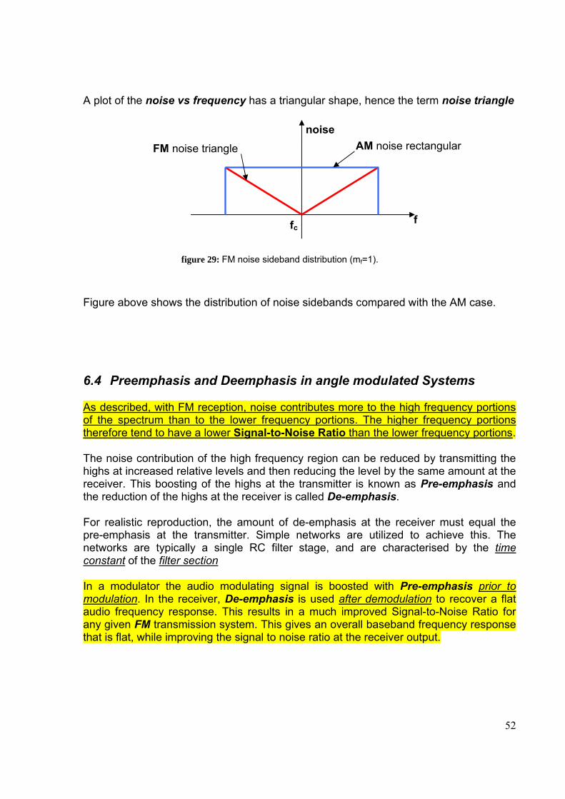
52
A plot of the noise vs frequency has a triangular shape, hence the term noise triangle
figure 29: FM noise sideband distribution (mf=1).
Figure above shows the distribution of noise sidebands compared with the AM case.
6.4 Preemphasis and Deemphasis in angle modulated Systems
As described, with FM reception, noise contributes more to the high frequency portions of the spectrum than to the lower frequency portions. The higher frequency portions therefore tend to have a lower Signal-to-Noise Ratio than the lower frequency portions.
The noise contribution of the high frequency region can be reduced by transmitting the highs at increased relative levels and then reducing the level by the same amount at the receiver. This boosting of the highs at the transmitter is known as Pre-emphasis and the reduction of the highs at the receiver is called De-emphasis.
For realistic reproduction, the amount of de-emphasis at the receiver must equal the pre-emphasis at the transmitter. Simple networks are utilized to achieve this. The networks are typically a single RC filter stage, and are characterised by the time constant of the filter section
In a modulator the audio modulating signal is boosted with Pre-emphasis prior to modulation. In the receiver, De-emphasis is used after demodulation to recover a flat audio frequency response. This results in a much improved Signal-to-Noise Ratio for any given FM transmission system. This gives an overall baseband frequency response that is flat, while improving the signal to noise ratio at the receiver output.
FM noise triangle AM noise rectangular
f fc
noise
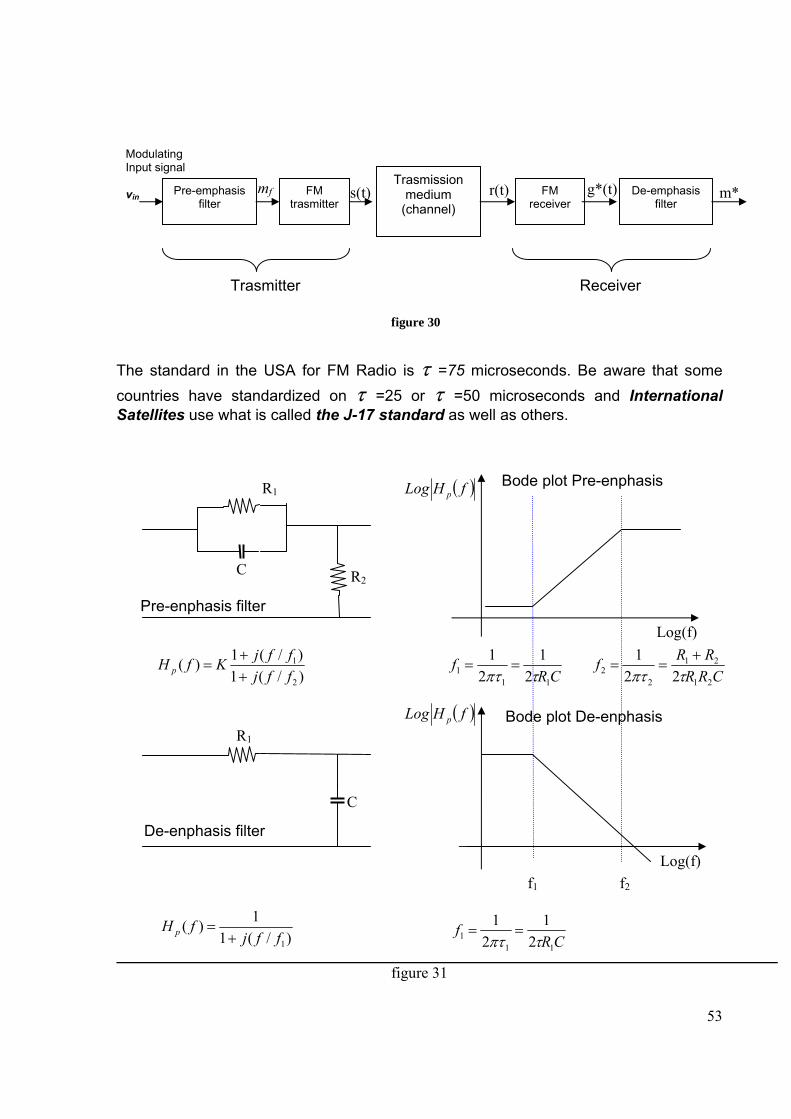
53
figure 30
The standard in the USA for FM Radio is τ =75 microseconds. Be aware that some countries have standardized on τ =25 or τ =50 microseconds and International Satellites use what is called the J-17 standard as well as others.
figure 31
R1
R1
C
C
R2
f1 f2
Log(f)
Log(f)
( )fHLog p
( )fHLog p
Pre-enphasis filter
De-enphasis filter
)/(1)/(1)(
2
1
ffjffjKfH p +
+=
CRRRRf
CRf
21
21
22
111 22
1 2
12
1τπττπτ+
====
)/(11)(
1ffjfH p +=
21
21
111 CR
fτπτ
==
Bode plot Pre-enphasis
Bode plot De-enphasis
Pre-emphasis filter
FM trasmitter
Trasmission medium
(channel) FM
receiver De-emphasis
filter mf s(t) r(t) g*(t) m*
Trasmitter Receiver
Modulating Input signal vin
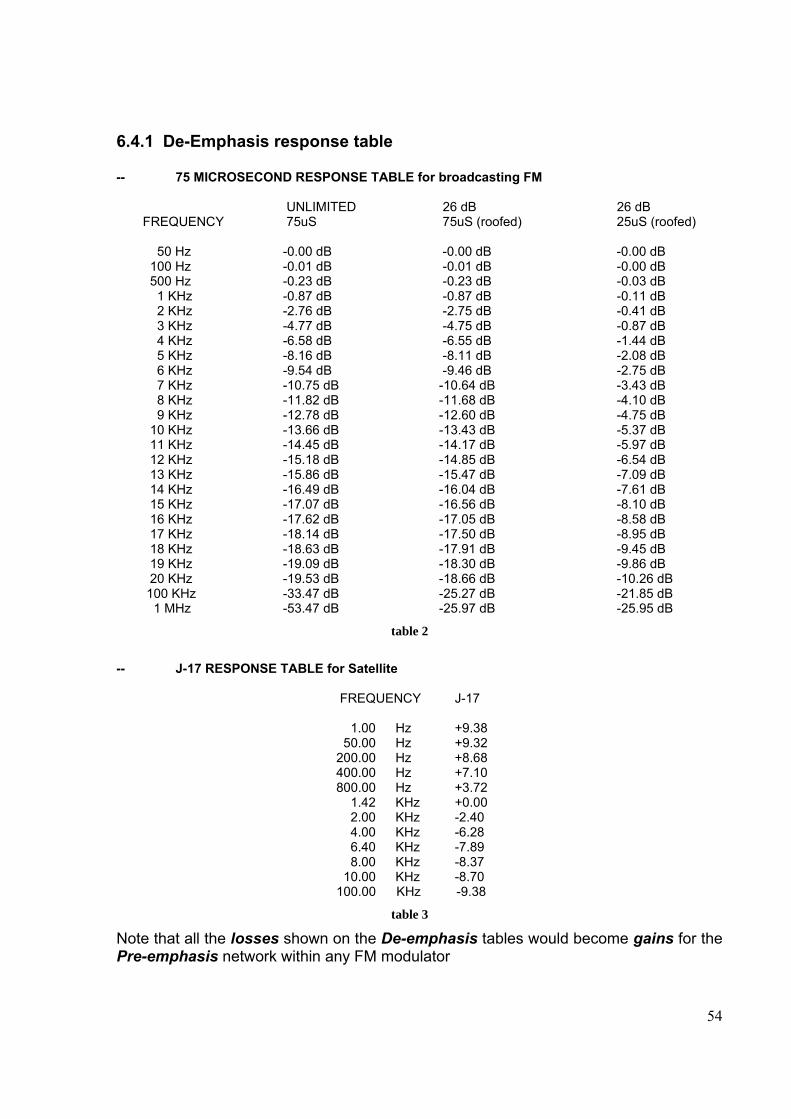
54
6.4.1 De-Emphasis response table -- 75 MICROSECOND RESPONSE TABLE for broadcasting FM
UNLIMITED 26 dB 26 dB FREQUENCY 75uS 75uS (roofed) 25uS (roofed) 50 Hz -0.00 dB -0.00 dB -0.00 dB 100 Hz -0.01 dB -0.01 dB -0.00 dB 500 Hz -0.23 dB -0.23 dB -0.03 dB 1 KHz -0.87 dB -0.87 dB -0.11 dB 2 KHz -2.76 dB -2.75 dB -0.41 dB 3 KHz -4.77 dB -4.75 dB -0.87 dB 4 KHz -6.58 dB -6.55 dB -1.44 dB 5 KHz -8.16 dB -8.11 dB -2.08 dB 6 KHz -9.54 dB -9.46 dB -2.75 dB 7 KHz -10.75 dB -10.64 dB -3.43 dB 8 KHz -11.82 dB -11.68 dB -4.10 dB 9 KHz -12.78 dB -12.60 dB -4.75 dB 10 KHz -13.66 dB -13.43 dB -5.37 dB 11 KHz -14.45 dB -14.17 dB -5.97 dB 12 KHz -15.18 dB -14.85 dB -6.54 dB 13 KHz -15.86 dB -15.47 dB -7.09 dB 14 KHz -16.49 dB -16.04 dB -7.61 dB 15 KHz -17.07 dB -16.56 dB -8.10 dB 16 KHz -17.62 dB -17.05 dB -8.58 dB 17 KHz -18.14 dB -17.50 dB -8.95 dB 18 KHz -18.63 dB -17.91 dB -9.45 dB 19 KHz -19.09 dB -18.30 dB -9.86 dB 20 KHz -19.53 dB -18.66 dB -10.26 dB 100 KHz -33.47 dB -25.27 dB -21.85 dB 1 MHz -53.47 dB -25.97 dB -25.95 dB
table 2
-- J-17 RESPONSE TABLE for Satellite
FREQUENCY J-17 1.00 Hz +9.38 50.00 Hz +9.32 200.00 Hz +8.68 400.00 Hz +7.10 800.00 Hz +3.72 1.42 KHz +0.00 2.00 KHz -2.40 4.00 KHz -6.28 6.40 KHz -7.89 8.00 KHz -8.37 10.00 KHz -8.70 100.00 KHz -9.38
table 3
Note that all the losses shown on the De-emphasis tables would become gains for the Pre-emphasis network within any FM modulator
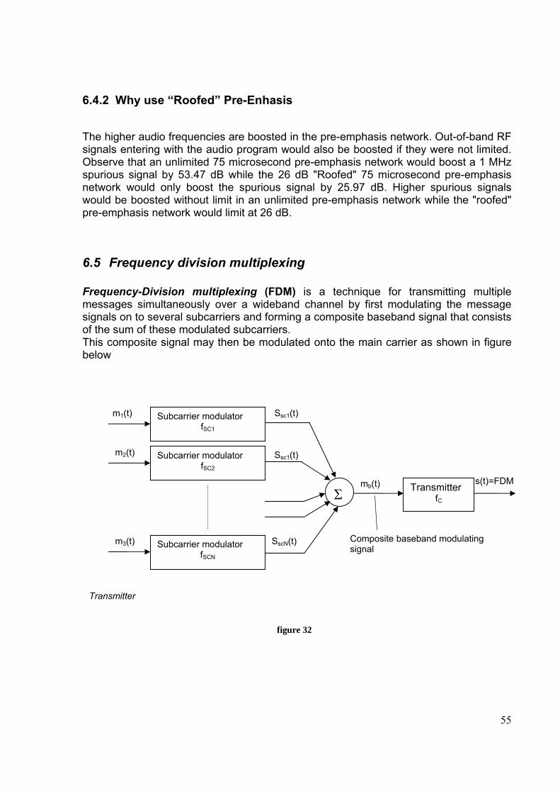
55
6.4.2 Why use “Roofed” Pre-Enhasis
The higher audio frequencies are boosted in the pre-emphasis network. Out-of-band RF signals entering with the audio program would also be boosted if they were not limited. Observe that an unlimited 75 microsecond pre-emphasis network would boost a 1 MHz spurious signal by 53.47 dB while the 26 dB "Roofed" 75 microsecond pre-emphasis network would only boost the spurious signal by 25.97 dB. Higher spurious signals would be boosted without limit in an unlimited pre-emphasis network while the "roofed" pre-emphasis network would limit at 26 dB.
6.5 Frequency division multiplexing Frequency-Division multiplexing (FDM) is a technique for transmitting multiple messages simultaneously over a wideband channel by first modulating the message signals on to several subcarriers and forming a composite baseband signal that consists of the sum of these modulated subcarriers. This composite signal may then be modulated onto the main carrier as shown in figure below
figure 32
Subcarrier modulator fSC1
Subcarrier modulator fSC2
Subcarrier modulator fSCN
Σ Transmitter fC
m1(t)
m2(t)
m3(t)
Ssc1(t)
Ssc1(t)
SscN(t)
mb(t) s(t)=FDM
Composite baseband modulating signal
Transmitter
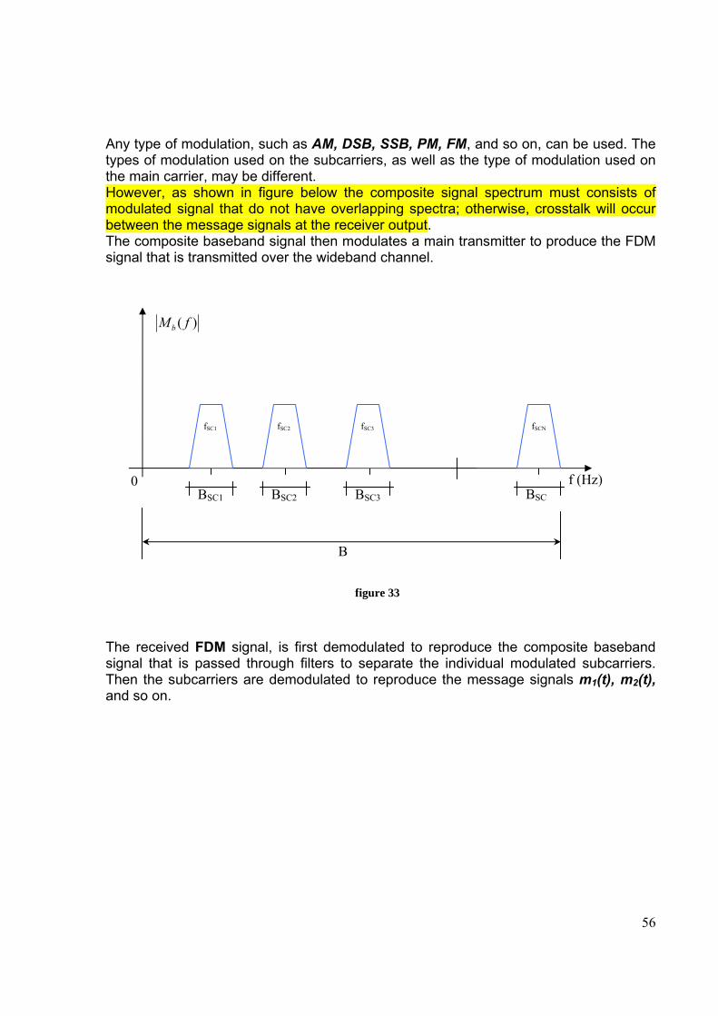
56
Any type of modulation, such as AM, DSB, SSB, PM, FM, and so on, can be used. The types of modulation used on the subcarriers, as well as the type of modulation used on the main carrier, may be different. However, as shown in figure below the composite signal spectrum must consists of modulated signal that do not have overlapping spectra; otherwise, crosstalk will occur between the message signals at the receiver output. The composite baseband signal then modulates a main transmitter to produce the FDM signal that is transmitted over the wideband channel.
figure 33
The received FDM signal, is first demodulated to reproduce the composite baseband signal that is passed through filters to separate the individual modulated subcarriers. Then the subcarriers are demodulated to reproduce the message signals m1(t), m2(t), and so on.
f (Hz)
)( fMb
0
fSC2 fSC3 fSCN
BSC1
fSC1
BSC2 BSC3 BSC
B
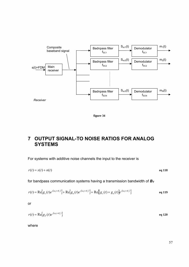
57
figure 34
7 OUTPUT SIGNAL-TO NOISE RATIOS FOR ANALOG SYSTEMS
For systems with additive noise channels the input to the receiver is
)()()( tntstr += eq 118
for bandpass communication systems having a transmission bandwidth of BT
( ){ } ( ){ } [ ] ( ){ }cccccc tjns
tjn
tjs etgtgetgetgtr θωθωθω +++ +=+= )()(Re)(Re)(Re)( eq 119
or
( ){ }cctjT etgtr θω += )(Re)( eq 120
where
Badnpass filter fSC1
Badnpass filter fSC2
Badnpass filter fSCN
Main receiver
m1(t)
m2(t)
mN(t)
Ssc1(t)
Receiver
Demodulator fSC1
Demodulator fSC2
Demodulator fSCN
s(t)=FDM
Ssc2(t)
Ssc3(t)
Composite baseband signal
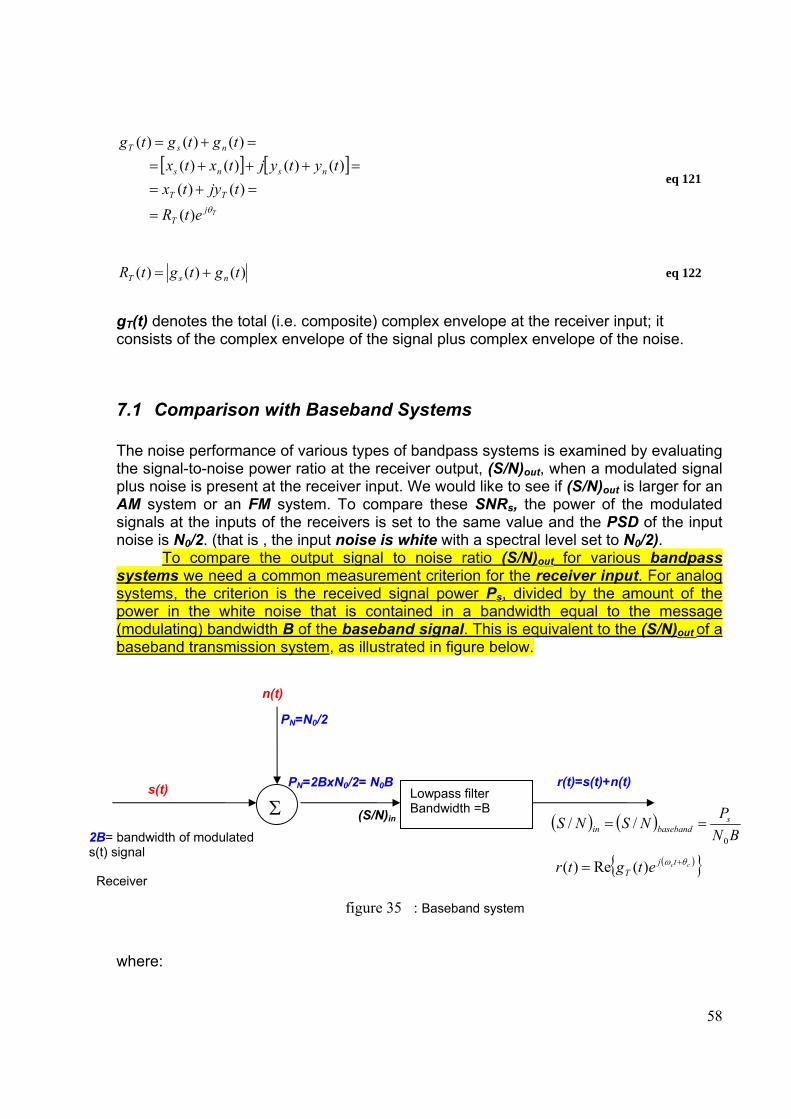
58
[ ] [ ]
TjT
TT
nsns
nsT
etR
tjytxtytyjtxtx
tgtgtg
θ)(
)()( )()()()(
)()()(
=
=+==+++=
=+=
eq 121
)()()( tgtgtR nsT += eq 122
gT(t) denotes the total (i.e. composite) complex envelope at the receiver input; it consists of the complex envelope of the signal plus complex envelope of the noise.
7.1 Comparison with Baseband Systems The noise performance of various types of bandpass systems is examined by evaluating the signal-to-noise power ratio at the receiver output, (S/N)out, when a modulated signal plus noise is present at the receiver input. We would like to see if (S/N)out is larger for an AM system or an FM system. To compare these SNRs, the power of the modulated signals at the inputs of the receivers is set to the same value and the PSD of the input noise is N0/2. (that is , the input noise is white with a spectral level set to N0/2).
To compare the output signal to noise ratio (S/N)out for various bandpass systems we need a common measurement criterion for the receiver input. For analog systems, the criterion is the received signal power Ps, divided by the amount of the power in the white noise that is contained in a bandwidth equal to the message (modulating) bandwidth B of the baseband signal. This is equivalent to the (S/N)out of a baseband transmission system, as illustrated in figure below.
figure 35 : Baseband system
where:
Σ Lowpass filter Bandwidth =B
n(t)
s(t)
PN=N0/2
r(t)=s(t)+n(t)
2B= bandwidth of modulated s(t) signal
( ) ( )BN
PNSNS sbasebandin
0
// == (S/N)in
PN=2BxN0/2= N0B
Receiver ( ){ }cctj
T etgtr θω += )(Re)(
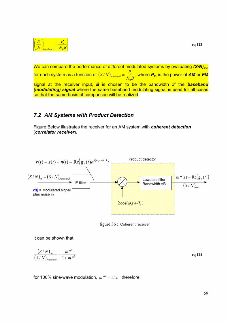
59
BNP
NS s
baseband 0
=⎟⎠⎞
⎜⎝⎛
eq 123
We can compare the performance of different modulated systems by evaluating (S/N)out
for each system as a function of ( )BN
PNS sbaseband
0
/ = , where Ps, is the power of AM or FM
signal at the receiver input, B is chosen to be the bandwidth of the baseband (modulating) signal where the same baseband modulating signal is used for all cases so that the same basis of comparison will be realized.
7.2 AM Systems with Product Detection Figure Below illustrates the receiver for an AM system with coherent detection (correlator receiver).
figure 36 : Coherent receiver
it can be shown that
( )( ) 2
2
*1*
//
mm
NSNS
baseband
out
+= eq 124
for 100% sine-wave modulation, 2/1*2 =m therefore
Lowpass filter Bandwidth =B
r(t) = Modulated signal plus noise in
Product detector
( )outNS / IF filter
{ })(Re)(* tgtm T=
)cos(2 cct θω +
( ){ }cctjT etgtntstr θω +=+= )(Re)()()(
( ) ( )basebandin NSNS // =
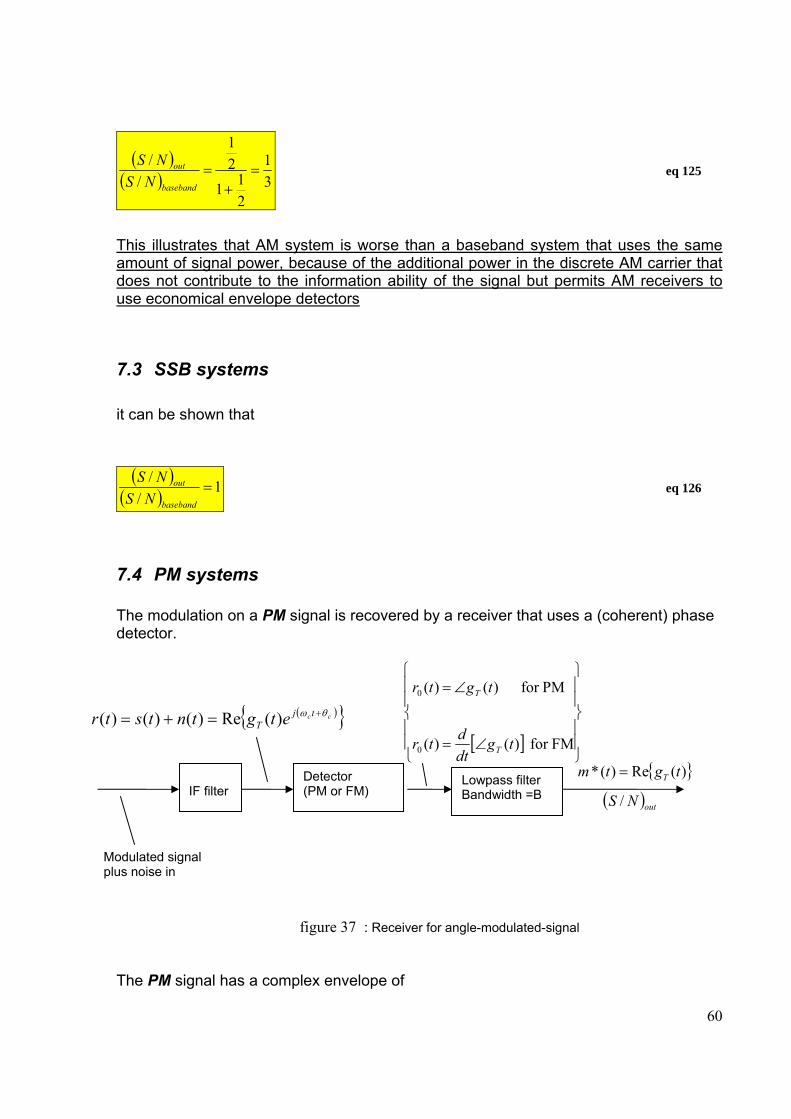
60
( )( ) 3
1
211
21
//
=+
=baseband
out
NSNS
eq 125
This illustrates that AM system is worse than a baseband system that uses the same amount of signal power, because of the additional power in the discrete AM carrier that does not contribute to the information ability of the signal but permits AM receivers to use economical envelope detectors
7.3 SSB systems
it can be shown that
( )( ) 1
//
=baseband
out
NSNS
eq 126
7.4 PM systems The modulation on a PM signal is recovered by a receiver that uses a (coherent) phase detector.
figure 37 : Receiver for angle-modulated-signal The PM signal has a complex envelope of
Lowpass filter Bandwidth =B
Modulated signal plus noise in
( )outNS / IF filter
{ })(Re)(* tgtm T=
[ ] ⎪⎪
⎭
⎪⎪
⎬
⎫
⎪⎪
⎩
⎪⎪
⎨
⎧
∠=
∠=
FMfor )()(
PMfor )()(
0
0
tgdtdtr
tgtr
T
T
( ){ }cctjT etgtntstr θω +=+= )(Re)()()(
Detector (PM or FM)
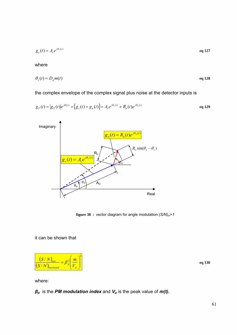
61
)()( tj
csseAtg θ= eq 127
where
)()( tmDt ps =θ eq 128
the complex envelope of the complex signal plus noise at the detector inputs is
[ ] )()()( )()()()()( tjn
tjcns
tjTT
ns etReAtgtgetgtg θθθ +=+== eq 129
figure 38 : vector diagram for angle modulation (S/N)in>1
it can be shown that
( )( )
2
2
//
⎟⎟⎠
⎞⎜⎜⎝
⎛=
pp
baseband
out
Vm
NSNS β eq 130
where: βp is the PM modulation index and Vp is the peak value of m(t).
Real
Imaginary
θs θT AC
θn
Rn( )tj
csseAtg θ=)(
( )tjnn
netRtg θ)()( =
)sin( snnR θθ −
62
This equation shows that the improvement of a PM system over a baseband signalling system depends on amount of phase deviation that is used; the larger the phase deviation, the better the signal-to-noise-ratio. It seems to indicate that we can make the improvement as large as we wish simply by increasing βp. This depends on the types of circuits used. If the peak phase deviation exceed π radians, special “phase unwrapping” techniques have to be used in some circuits to obtain the true value (as compared to the relative value) of the phase output.
Thus the maximum value of )()(
tmDV
tmp
p
p =β
might be taken to be π. For sinusoidal
modulation, this would provide an improvement of [ ] dBmDV
mp
p
p 9.62
22
2
≅==⎥⎥⎦
⎤
⎢⎢⎣
⎡ πβ over
baseband signaling. It is emphasized that the results obtained previously for (S/N)out are valid only when the input signal is above the threshold [i.e. when (S/N)in>1]
7.5 FM Systems The procedure that we will use to evaluate the output SNR for FM systems is essentially the same as that used for PM systems, except that the output for the FM detector is proportional to dθ(t)/dt, whereas the output of the PM detector is proportional to θ(t). assuming that (S/N)in>1 then we can find
( )( )
2
23/
/⎟⎟⎠
⎞⎜⎜⎝
⎛=
pf
baseband
out
Vm
NSNS β eq 131
for the case of sinusoidal modulation 21
2
=⎟⎟⎠
⎞⎜⎜⎝
⎛
pVm we have
( )( )
2
23
//
fbaseband
out
NSNS β=
At first glance, these results seem to indicate that the performance of FM systems can be increased without limit simply by increasing the FM index βf. However, as βf is increased, the transmission bandwidth increases, and consequently, (S/N)in decreases. These equations for (S/N)out are valid only when (S/N)in >>1 (i.e. when the input signal power is above the threshold), so (S/N)out does not increase to an excessively large value simply by increasing the FM index βf. Figure below, by dashed line, show a plot of the preceding equation.
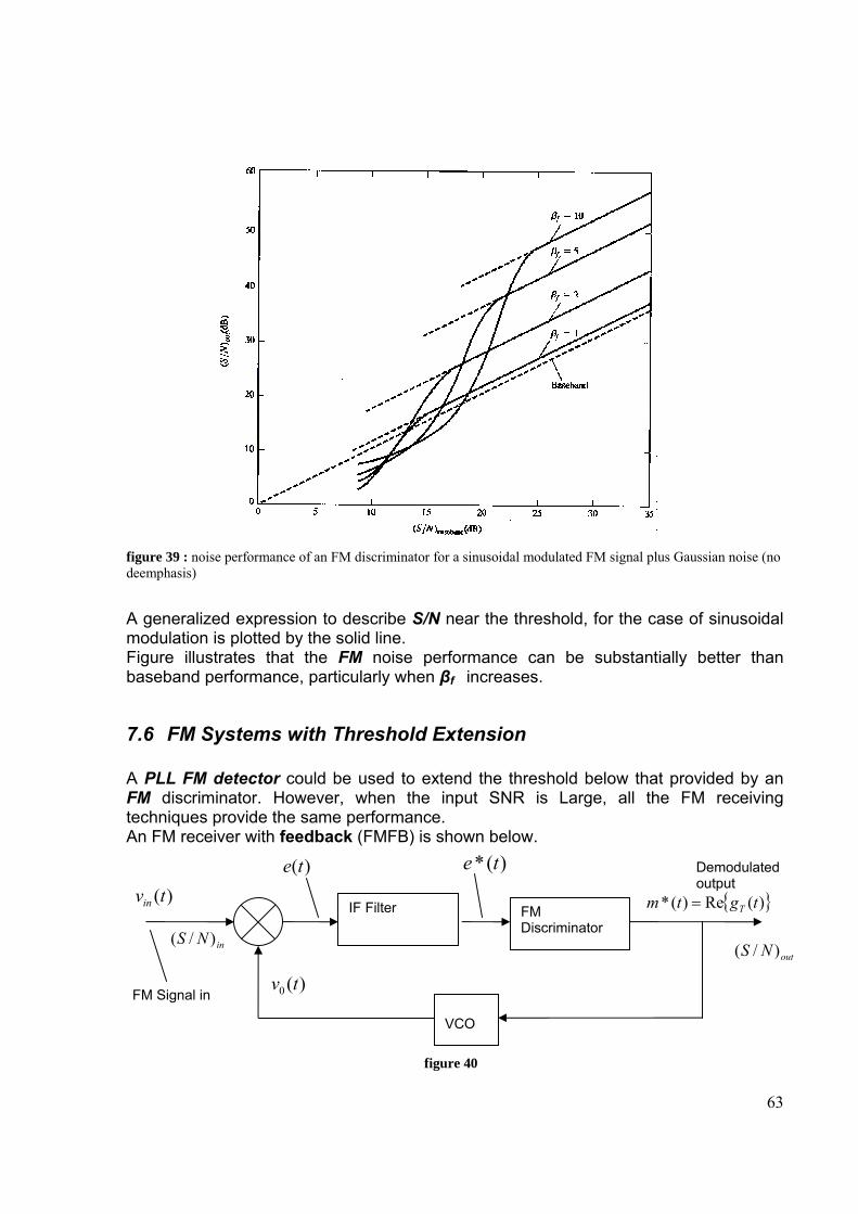
63
figure 39 : noise performance of an FM discriminator for a sinusoidal modulated FM signal plus Gaussian noise (no deemphasis)
A generalized expression to describe S/N near the threshold, for the case of sinusoidal modulation is plotted by the solid line. Figure illustrates that the FM noise performance can be substantially better than baseband performance, particularly when βf increases.
7.6 FM Systems with Threshold Extension A PLL FM detector could be used to extend the threshold below that provided by an FM discriminator. However, when the input SNR is Large, all the FM receiving techniques provide the same performance. An FM receiver with feedback (FMFB) is shown below.
figure 40
FM Discriminator
FM Signal in
outNS )/(
VCO
{ })(Re)(* tgtm T=
)(* te )(te
IF Filter )(tvin
)(0 tv
Demodulated output
inNS )/(
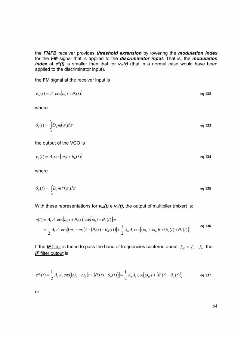
64
the FMFB receiver provides threshold extension by lowering the modulation index for the FM signal that is applied to the discriminator input. That is, the modulation index of e*(t) is smaller than that for vin(t) (that in a normal case would have been applied to the discriminator input). the FM signal at the receiver input is
[ ])(cos)( ttAtv iccin θω += eq 132
where
( ) σσθ dmDtt
fi ∫∞−
=)( eq 133
the output of the VCO is
[ ])(cos)( 0000 ttAtv θω += eq 134
where
( ) σσθ dmDtt
v∫∞−
= *)(0 eq 135
With these representations for vin(t) e v0(t), the output of multiplier (mixer) is:
[ ] [ ]
( ) ( )[ ] ( ) ( )[ ])()(cos21)()(cos
21
)(cos)(cos)(
000000
000
tttAAtttAA
ttttAAte
iccicc
icc
θθωωθθωω
θωθω
++++−+−=
=++= eq 136
If the IF filter is tuned to pass the band of frequencies centered about 0fff cIF −≡ , the IF filter output is
( ) ( )[ ] ( )[ ])()(cos21)()(cos
21)(* 00000 tttAAtttAAte iIFcicc θθωθθωω −+=−+−= eq 137
or
65
[ ] ⎥⎦
⎤⎢⎣
⎡−+= ∫
∞−
t
vfifc dmDmDtAAte σσσω )(*)(cos21)(* 0 eq 138
the FM discriminator output is proportional to the derivative of the phase deviation
[ ]dt
dmDmDdKtm
t
vf⎭⎬⎫
⎩⎨⎧
−
=∫∞−
σσσ
π
)(*)(
2)(* eq 139
Evaluating the derivative and solving the resulting equation for m*(t), we obtain
[ ]
[ ]v
f
v
f
fv
fv
vfvf
KDtmKD
DK
tmDK
tmtmDKDKtm
tmDKtmDKtm
tmDKtmDKtmDtmDKtm
+=
⎥⎦⎤
⎢⎣⎡ +
=⇒=⎥⎦⎤
⎢⎣⎡ +
=+
−=−=
ππ
πππ
ππ
πππ
2 )(
21
)(2)(* )(
221)(*
)(2
)(*2
)(*
)(*2
)(2
)(*)(2
)(*
eq 140
)(2
)(* tmKD
KDtm
v
f⎟⎟⎠
⎞⎜⎜⎝
⎛+
=π
eq 141
Substituting this expression for m*(t) we get
⎥⎥⎥⎥
⎦
⎤
⎢⎢⎢⎢
⎣
⎡
⎟⎟⎟⎟
⎠
⎞
⎜⎜⎜⎜
⎝
⎛
⎟⎠⎞
⎜⎝⎛+
+=
⎥⎦
⎤⎢⎣
⎡⎥⎦
⎤⎢⎣
⎡+
−++=
⎥⎥⎦
⎤
⎢⎢⎣
⎡⎥⎦
⎤⎢⎣
⎡⎟⎟⎠
⎞⎜⎜⎝
⎛+
−+=
∫
∫
∫
∞−
∞−
∞−
t
f
v
IFc
t
v
fvvfIFc
t
v
fvfIFc
dmDDk
tAA
dKD
mKDDmKDmDtAA
dmKD
KDDmDtAAte
σσ
π
ω
σπ
σσσπω
σσπ
σω
)(
21
1cos21
2)()()(2
cos21
)(2
)(cos21)(*
0
0
0
eq 142
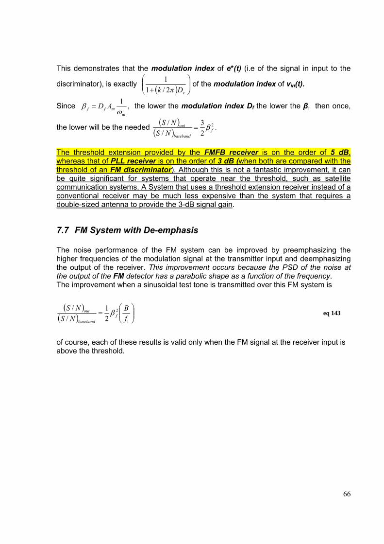
66
This demonstrates that the modulation index of e*(t) (i.e of the signal in input to the
discriminator), is exactly ( ) ⎟⎟⎠
⎞⎜⎜⎝
⎛+ vDk π2/1
1 of the modulation index of vin(t).
Since m
mff ADω
β 1= , the lower the modulation index Df the lower the β, then once,
the lower will be the needed ( )( )
2
23
//
fbaseband
out
NSNS β= .
The threshold extension provided by the FMFB receiver is on the order of 5 dB, whereas that of PLL receiver is on the order of 3 dB (when both are compared with the threshold of an FM discriminator). Although this is not a fantastic improvement, it can be quite significant for systems that operate near the threshold, such as satellite communication systems. A System that uses a threshold extension receiver instead of a conventional receiver may be much less expensive than the system that requires a double-sized antenna to provide the 3-dB signal gain.
7.7 FM System with De-emphasis The noise performance of the FM system can be improved by preemphasizing the higher frequencies of the modulation signal at the transmitter input and deemphasizing the output of the receiver. This improvement occurs because the PSD of the noise at the output of the FM detector has a parabolic shape as a function of the frequency. The improvement when a sinusoidal test tone is transmitted over this FM system is
( )( ) ⎟⎟
⎠
⎞⎜⎜⎝
⎛=
1
2
21
//
fB
NSNS
fbaseband
out β eq 143
of course, each of these results is valid only when the FM signal at the receiver input is above the threshold.
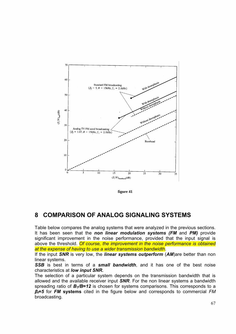
67
figure 41
8 COMPARISON OF ANALOG SIGNALING SYSTEMS Table below compares the analog systems that were analyzed in the previous sections. It has been seen that the non linear modulation systems (FM and PM) provide significant improvement in the noise performance, provided that the input signal is above the threshold. Of course, the improvement in the noise performance is obtained at the expense of having to use a wider transmission bandwidth. If the input SNR is very low, the linear systems outperform (AM)are better than non linear systems. SSB is best in terms of a small bandwidth, and it has one of the best noise characteristics at low input SNR. The selection of a particular system depends on the transmission bandwidth that is allowed and the available receiver input SNR. For the non linear systems a bandwidth spreading ratio of BT/B=12 is chosen for systems comparisons. This corresponds to a βf=5 for FM systems cited in the figure below and corresponds to commercial FM broadcasting.
68
Of course, when operating above the threshold, all the non linear modulation systems have better SNR performance than the linear modulation systems, because the non linear systems have larger transmission bandwidths.
8.1 Ideal systems performance What is the best noise performance that is theoretically possible? How can wide transmission bandwidth be used to gain improved noise performance? The answer is given by Shannon’s channel capacity theorem. The ideal system is defined as one that does not lose channel capacity in the detection process.
outin CC = eq 144
where Cin is the bandpass channel capacity and Cout is the channel capacity after detection. The equation for channel capacity is
⎟⎠⎞
⎜⎝⎛ +=
NSBC 1log2 eq 145
using this equation in the preceding equation we get:
⎥⎦
⎤⎢⎣
⎡⎟⎠⎞
⎜⎝⎛+=⎥
⎦
⎤⎢⎣
⎡⎟⎠⎞
⎜⎝⎛+
outinT N
SBNSB 1log1log 22 eq 146
where BT is the transmission bandwidth of the bandpass signal at the receiver input and B is the bandwidth of the baseband signal at the receiver output. Solving for (S/N)out , we get
out
BB
in
B
out
B
in NS
NS
NS
NS
TT
⎟⎠⎞
⎜⎝⎛+=⎥
⎦
⎤⎢⎣
⎡⎟⎠⎞
⎜⎝⎛+⇒⎥
⎦
⎤⎢⎣
⎡⎟⎠⎞
⎜⎝⎛+=⎥
⎦
⎤⎢⎣
⎡⎟⎠⎞
⎜⎝⎛+ 1 1 11 eq 147
11 −⎥⎦
⎤⎢⎣
⎡⎟⎠⎞
⎜⎝⎛+=⎟
⎠⎞
⎜⎝⎛ B
B
inout
T
NS
NS
eq 148
but
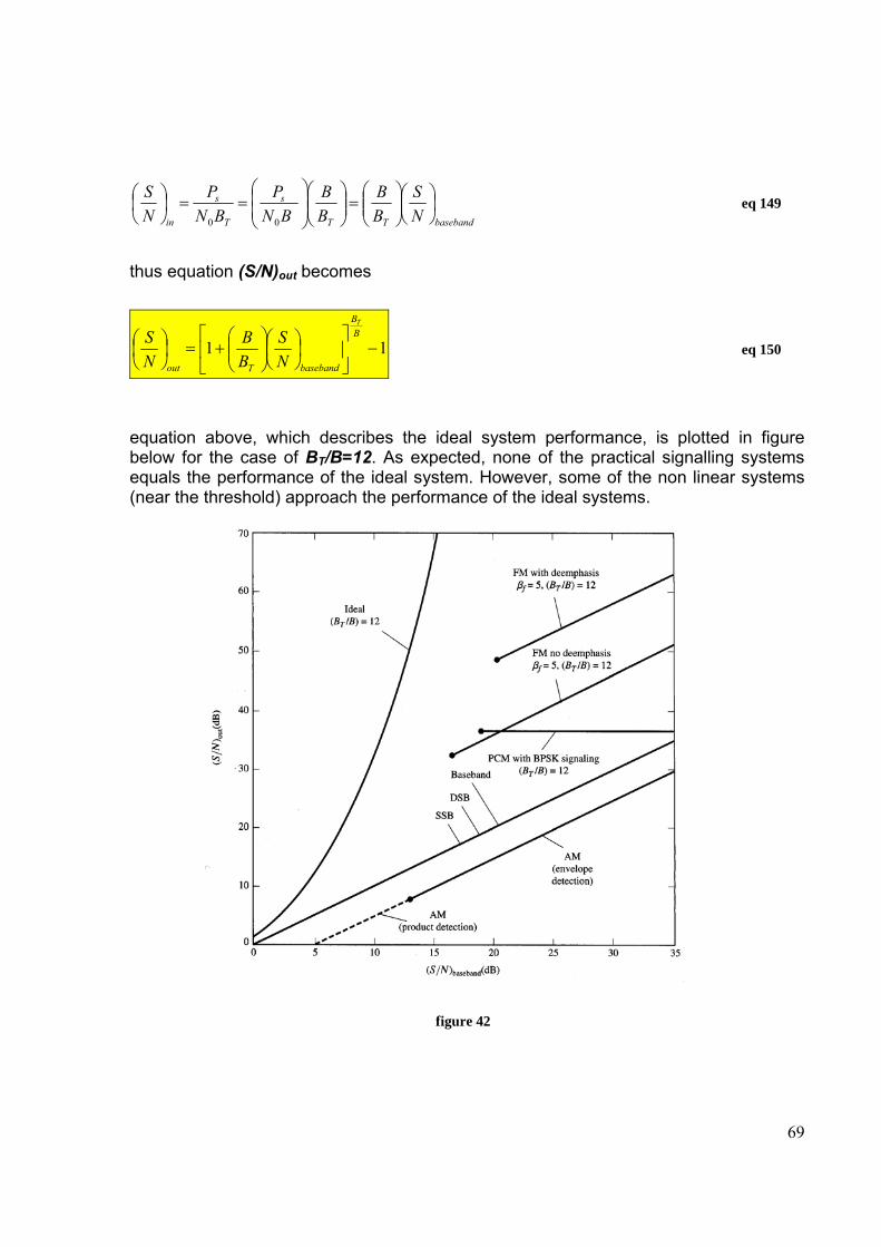
69
basebandTT
s
T
s
in NS
BB
BB
BNP
BNP
NS
⎟⎠⎞
⎜⎝⎛⎟⎟⎠
⎞⎜⎜⎝
⎛=⎟⎟
⎠
⎞⎜⎜⎝
⎛⎟⎟⎠
⎞⎜⎜⎝
⎛==⎟
⎠⎞
⎜⎝⎛
00
eq 149
thus equation (S/N)out becomes
11 −⎥⎦
⎤⎢⎣
⎡⎟⎠⎞
⎜⎝⎛⎟⎟⎠
⎞⎜⎜⎝
⎛+=⎟
⎠⎞
⎜⎝⎛ B
B
basebandTout
T
NS
BB
NS
eq 150
equation above, which describes the ideal system performance, is plotted in figure below for the case of BT/B=12. As expected, none of the practical signalling systems equals the performance of the ideal system. However, some of the non linear systems (near the threshold) approach the performance of the ideal systems.
figure 42
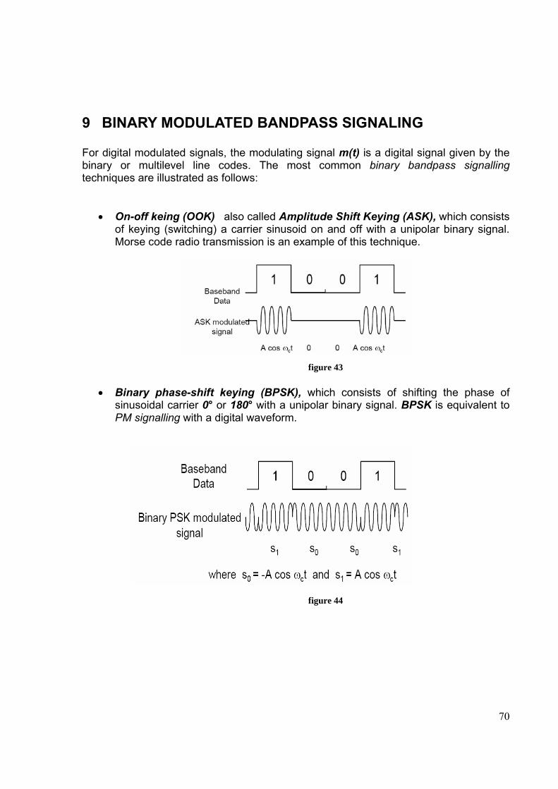
70
9 BINARY MODULATED BANDPASS SIGNALING For digital modulated signals, the modulating signal m(t) is a digital signal given by the binary or multilevel line codes. The most common binary bandpass signalling techniques are illustrated as follows:
• On-off keing (OOK) also called Amplitude Shift Keying (ASK), which consists of keying (switching) a carrier sinusoid on and off with a unipolar binary signal. Morse code radio transmission is an example of this technique.
figure 43
• Binary phase-shift keying (BPSK), which consists of shifting the phase of sinusoidal carrier 0° or 180° with a unipolar binary signal. BPSK is equivalent to PM signalling with a digital waveform.
figure 44
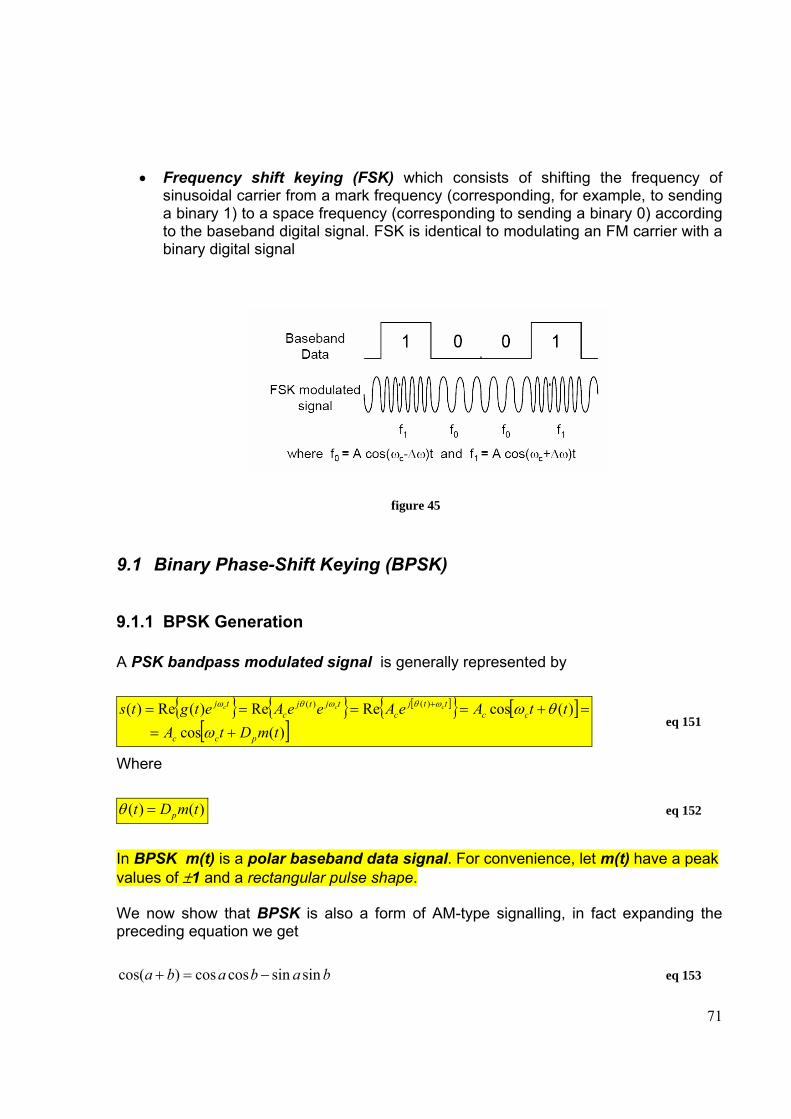
71
• Frequency shift keying (FSK) which consists of shifting the frequency of sinusoidal carrier from a mark frequency (corresponding, for example, to sending a binary 1) to a space frequency (corresponding to sending a binary 0) according to the baseband digital signal. FSK is identical to modulating an FM carrier with a binary digital signal
figure 45
9.1 Binary Phase-Shift Keying (BPSK)
9.1.1 BPSK Generation A PSK bandpass modulated signal is generally represented by
{ } { } [ ]{ } [ ][ ])(cos
)(cosReRe)(Re)( )()(
tmDtAttAeAeeAetgts
pcc
ccttj
ctjtj
ctj ccc
+==+==== +
ωθωωθωθω
eq 151
Where
)()( tmDt p=θ eq 152
In BPSK m(t) is a polar baseband data signal. For convenience, let m(t) have a peak values of ±1 and a rectangular pulse shape. We now show that BPSK is also a form of AM-type signalling, in fact expanding the preceding equation we get
bababa sinsincoscos)cos( −=+ eq 153
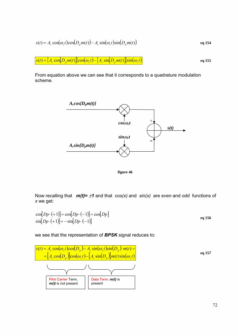
72
( ) ( ) ( ) ( ))(sinsin)(coscos)( tmDtAtmDtAts pccpcc ωω −= eq 154
[ ]{ } ( ) [ ]{ } ( )ttmDAttmDAts cpccpc ωω sin)(sincos)(cos)( −= eq 155
From equation above we can see that it corresponds to a quadrature modulation scheme.
figure 46
Now recalling that m(t)= ±1 and that cos(x) and sin(x) are even and odd functions of x we get:
( )[ ] ( )[ ] [ ]( )[ ] ( )[ ]1sin1sin
cos1cos1cos−⋅−=+⋅
=−⋅=+⋅DpDp
DpDpDp eq 156
we see that the representation of BPSK signal reduces to:
( ) ( ) ( ) ( )( )[ ] ( ) ( )[ ] ( )ttmDAtDA
tmDtADtAts
cpccpc
pccpcc
ωω
ωω
sin)(sincoscos
)(sinsincoscos)(
−=
=⋅−= eq 157
s(t) +
-
Accos[Dpm(t)]
Acsin[Dpm(t)]
cosωct
sinωct
Pilot Carrier Term, m(t) is not present
Data Term: m(t) is present
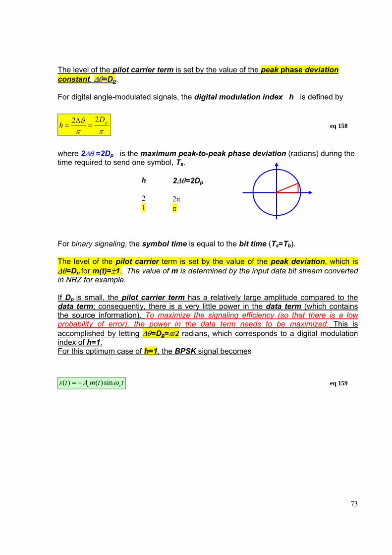
73
The level of the pilot carrier term is set by the value of the peak phase deviation constant, ∆θ=Dp. For digital angle-modulated signals, the digital modulation index h is defined by
ππϑ pD
h22
=∆
= eq 158
where 2∆θ =2Dp is the maximum peak-to-peak phase deviation (radians) during the time required to send one symbol, Ts.
h 2∆θ=2Dp
2 2π 1 π
For binary signaling, the symbol time is equal to the bit time (Ts=Tb). The level of the pilot carrier term is set by the value of the peak deviation, which is ∆θ=Dp for m(t)=±1. The value of m is determined by the input data bit stream converted in NRZ for example. If Dp is small, the pilot carrier term has a relatively large amplitude compared to the data term; consequently, there is a very little power in the data term (which contains the source information). To maximize the signaling efficiency (so that there is a low probability of error), the power in the data term needs to be maximized. This is accomplished by letting ∆θ=Dp=π/2 radians, which corresponds to a digital modulation index of h=1. For this optimum case of h=1, the BPSK signal becomes
ttmAts cc ωsin)()( −= eq 159
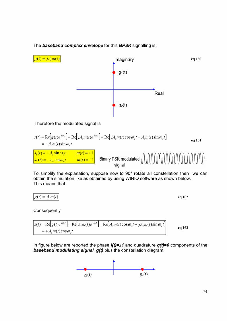
74
The baseband complex envelope for this BPSK signalling is:
)()( tmjAtg c= eq 160
Therefore the modulated signal is
[ ] [ ] [ ]ttmA
ttmAttmjAetmjAetgts
cc
cccctj
ctj cc
ωωωωω
sin)( sin)(cos)(Re)(Re)(Re)(
−=−===
eq 161
1)( sin)(1)( sin)(
2
1
−=+=+=−=
tmtAtstmtAts
cc
cc
ωω
To simplify the explanation, suppose now to 90° rotate all constellation then we can obtain the simulation like as obtained by using WINIQ software as shown below. This means that
)()( tmAtg c= eq 162
Consequently
[ ] [ ] [ ]ttmA
ttmjAttmAetmAetgts
cc
cccctj
ctj cc
ωωωωω
cos)( sin)(cos)(Re)(Re)(Re)(
+=+===
eq 163
In figure below are reported the phase i(t)=±1 and quadrature q(t)=0 components of the baseband modulating signal g(t) plus the constellation diagram.
g2(t)
g1(t)
Real
Imaginary
g1(t) g2(t)
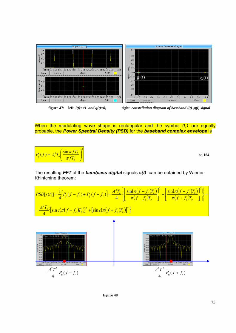
75
figure 47: left i(t)=±1 and q(t)=0, right constellation diagram of baseband i(t) ,q(t) signal
When the modulating wave shape is rectangular and the symbol 0,1 are equally probable, the Power Spectral Density (PSD) for the baseband complex envelope is
22 sin)( ⎟⎟
⎠
⎞⎜⎜⎝
⎛=
b
bbcg Tf
TfTAfPππ
eq 164
The resulting FFT of the bandpass digital signals s(t) can be obtained by Wiener-Khintchine theorem:
[ ] ( )( )( )
( )( )( )
( )( )[ ] ( )( )[ ]{ }222
222
sinsin4
sinsin4
)()(41)]([
bcbcb
bc
bc
bc
bcbcgcg
TffcTffcTA
TffTff
TffTffTAffPffPtsPSD
++−=
=⎪⎭
⎪⎬⎫
⎪⎩
⎪⎨⎧
⎥⎦
⎤⎢⎣
⎡++
+⎥⎦
⎤⎢⎣
⎡−−
=++−=
ππ
ππ
ππ
figure 48
g2(t) g1(t)
)(4
2
cg
b
ffPTA− )(
4
2
cg
b
ffPTA+
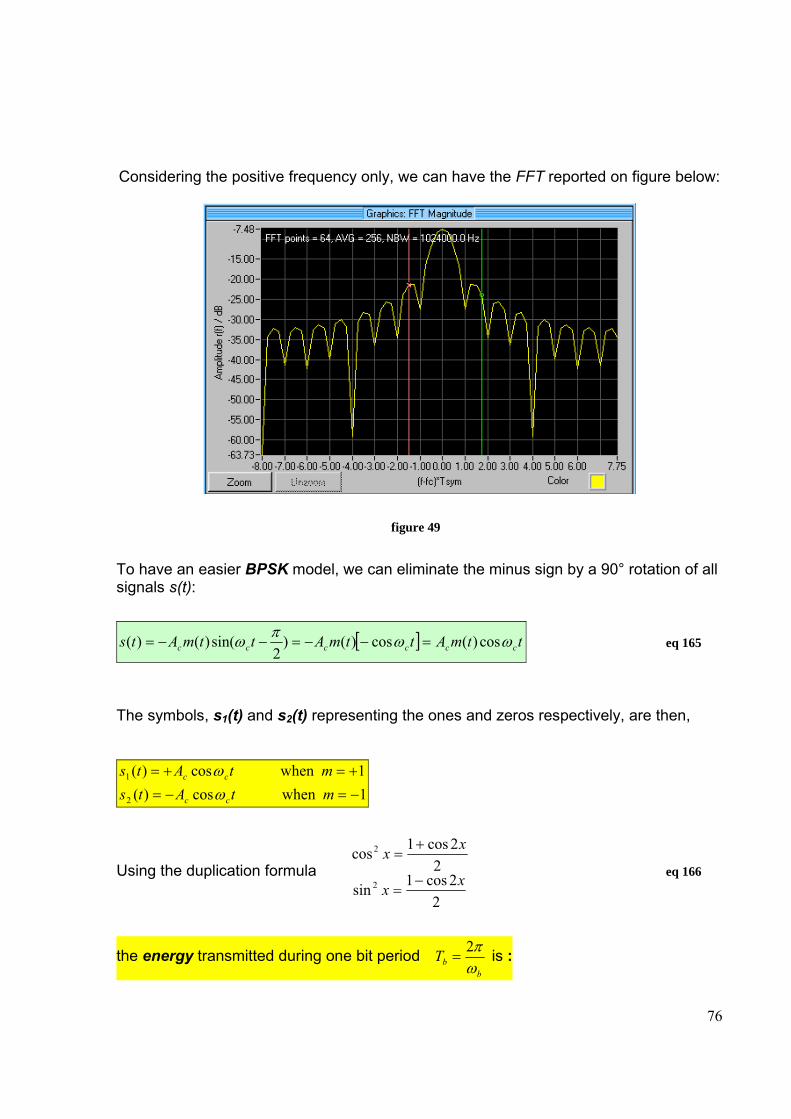
76
Considering the positive frequency only, we can have the FFT reported on figure below:
figure 49
To have an easier BPSK model, we can eliminate the minus sign by a 90° rotation of all signals s(t):
[ ] ttmAttmAttmAts cccccc ωωπω cos)(cos)()2
sin()()( =−−=−−= eq 165
The symbols, s1(t) and s2(t) representing the ones and zeros respectively, are then,
1 when cos)(1 when cos)(
2
1
−=−=+=+=
mtAtsmtAts
cc
cc
ωω
Using the duplication formula
22cos1sin
22cos1cos
2
2
xx
xx
−=
+=
eq 166
the energy transmitted during one bit period b
bTωπ2
= is :
77
( ) ( ) ( ) ( )
( )
( ) ( ) ....1,2,3,4...n with ,2 , where
20
2
22
21
222
21
2
2cos21
222cos1
ˆ
222
2
0
22
2
0
2
0
2
0
22
0
2
====
=
⎥⎥⎥⎥⎥
⎦
⎤
⎢⎢⎢⎢⎢
⎣
⎡
−⎟⎟⎠
⎞⎜⎜⎝
⎛
−=⎥⎦
⎤⎢⎣
⎡−
=⎥⎥⎥
⎦
⎤
⎢⎢⎢
⎣
⎡
−=−
=== ∫∫∫∫
bcb
bcc
bc
c
bc
cb
cc
cc
bc
cb
c
Tc
c
T
cc
T
b
nTtsenAts
TAsen
ATAtsenATA
dttTAdttAdttsenAdttsE
b
bbbb
ωωωπω
ωωπω
ωω
ωωω
ωπ
ωπ
eq 167
Therefore the carrier power, C, during a bit period Tb is:
[ ]WATEC c
b
b 2
2
== eq 168
The value AC of the carrier is given by:
b
bc T
EA 2= [V] eq 169
Substituting this value of Ac into equation of s(t) we get:
1 when cos2cos)()(
1 when cos2cos)()(
2
1
−=−==
+=+==
mtT
EttmAts
mtT
EttmAts
cb
bcc
cb
bcc
ωω
ωω
eq 170
This form of BPSK is referred to as phase-reversal keying since the two carrier signals representing the logic ones and zeros are exactly 180° out of the phase i.e. the phase modulation index h=1. A more general form of BPSK occurs when the phase difference between the two signals is other than 180°. This creates a residual carrier term that allows carrier tracking by a phase-lock loop (PLL). Unless stated otherwise, BPSK will refer to 180° mode.
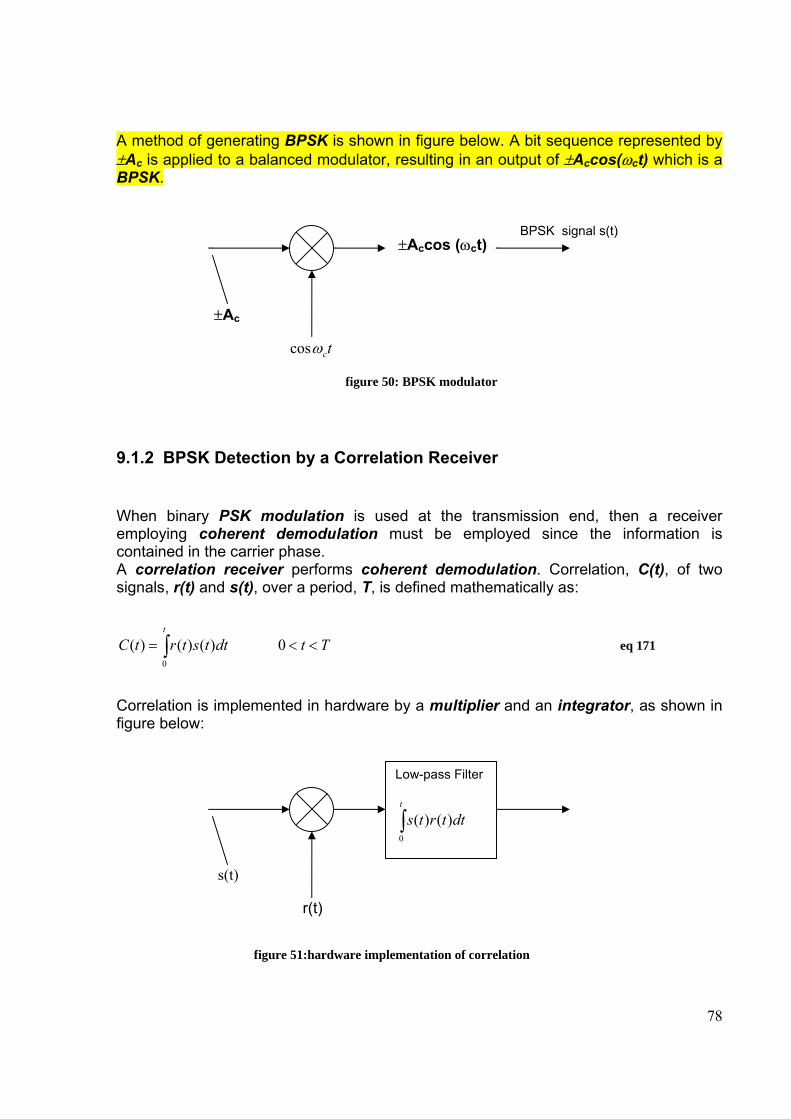
78
A method of generating BPSK is shown in figure below. A bit sequence represented by ±Ac is applied to a balanced modulator, resulting in an output of ±Accos(ωct) which is a BPSK.
figure 50: BPSK modulator
9.1.2 BPSK Detection by a Correlation Receiver When binary PSK modulation is used at the transmission end, then a receiver employing coherent demodulation must be employed since the information is contained in the carrier phase. A correlation receiver performs coherent demodulation. Correlation, C(t), of two signals, r(t) and s(t), over a period, T, is defined mathematically as:
∫ <<=t
TtdttstrtC0
0 )()()( eq 171
Correlation is implemented in hardware by a multiplier and an integrator, as shown in figure below:
figure 51:hardware implementation of correlation
r(t)
s(t)
Low-pass Filter
∫t
dttrts0
)()(
±Ac
tcωcos
BPSK signal s(t) ±Accos (ωct)
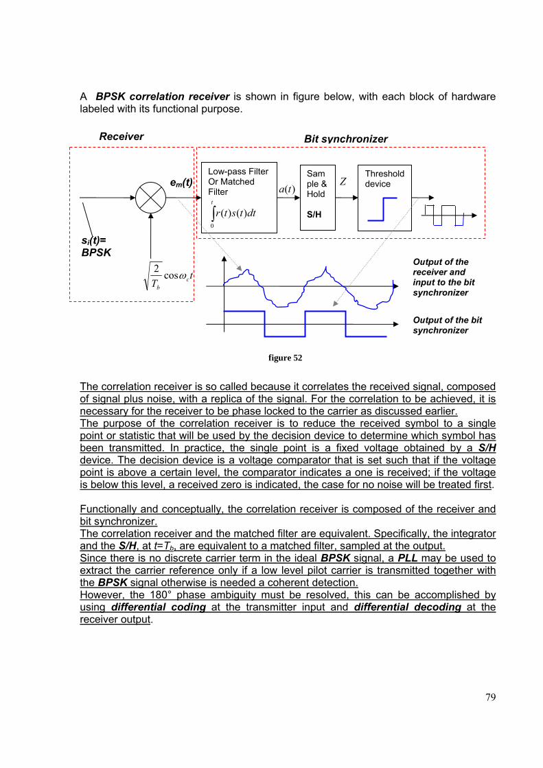
79
A BPSK correlation receiver is shown in figure below, with each block of hardware labeled with its functional purpose.
figure 52
The correlation receiver is so called because it correlates the received signal, composed of signal plus noise, with a replica of the signal. For the correlation to be achieved, it is necessary for the receiver to be phase locked to the carrier as discussed earlier. The purpose of the correlation receiver is to reduce the received symbol to a single point or statistic that will be used by the decision device to determine which symbol has been transmitted. In practice, the single point is a fixed voltage obtained by a S/H device. The decision device is a voltage comparator that is set such that if the voltage point is above a certain level, the comparator indicates a one is received; if the voltage is below this level, a received zero is indicated, the case for no noise will be treated first. Functionally and conceptually, the correlation receiver is composed of the receiver and bit synchronizer. The correlation receiver and the matched filter are equivalent. Specifically, the integrator and the S/H, at t=Tb, are equivalent to a matched filter, sampled at the output. Since there is no discrete carrier term in the ideal BPSK signal, a PLL may be used to extract the carrier reference only if a low level pilot carrier is transmitted together with the BPSK signal otherwise is needed a coherent detection. However, the 180° phase ambiguity must be resolved, this can be accomplished by using differential coding at the transmitter input and differential decoding at the receiver output.
si(t)=BPSK
tT c
b
ωcos2
Low-pass Filter Or Matched Filter
∫t
dttstr0
)()(
Sample & Hold S/H
Threshold device
em(t) )(taZ
Receiver Bit synchronizer
Output of the receiver and input to the bit synchronizer
Output of the bit synchronizer
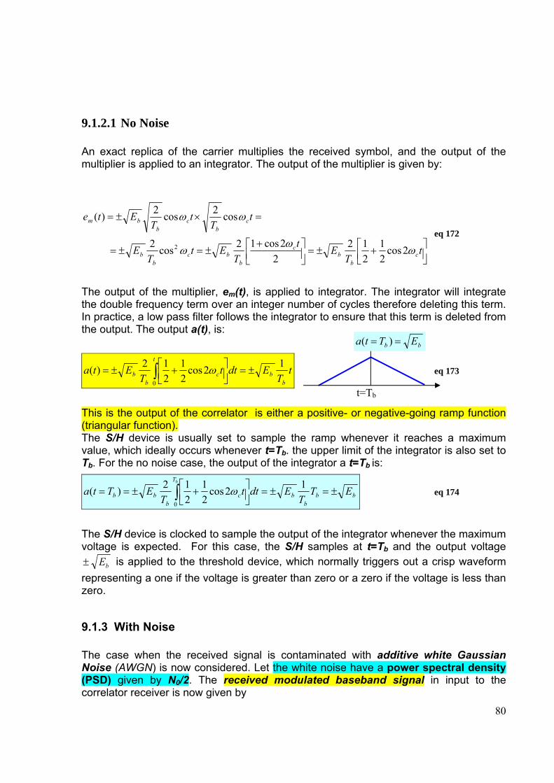
80
9.1.2.1 No Noise An exact replica of the carrier multiplies the received symbol, and the output of the multiplier is applied to an integrator. The output of the multiplier is given by:
⎥⎦⎤
⎢⎣⎡ +±=⎥⎦
⎤⎢⎣⎡ +
±=±=
=×±=
tT
EtT
EtT
E
tT
tT
Ete
cb
bc
bbc
bb
cb
cb
bm
ωω
ω
ωω
2cos21
212
22cos12cos2
cos2cos2)(
2
eq 172
The output of the multiplier, em(t), is applied to integrator. The integrator will integrate the double frequency term over an integer number of cycles therefore deleting this term. In practice, a low pass filter follows the integrator to ensure that this term is deleted from the output. The output a(t), is:
tT
EdttT
Etab
b
t
cb
b12cos
21
212)(
0
±=⎥⎦⎤
⎢⎣⎡ +±= ∫ ω eq 173
This is the output of the correlator is either a positive- or negative-going ramp function (triangular function). The S/H device is usually set to sample the ramp whenever it reaches a maximum value, which ideally occurs whenever t=Tb. the upper limit of the integrator is also set to Tb. For the no noise case, the output of the integrator a t=Tb is:
bbb
b
T
cb
bb ETT
EdttT
ETtab
±=±=⎥⎦⎤
⎢⎣⎡ +±== ∫
12cos21
212)(
0
ω eq 174
The S/H device is clocked to sample the output of the integrator whenever the maximum voltage is expected. For this case, the S/H samples at t=Tb and the output voltage
bE± is applied to the threshold device, which normally triggers out a crisp waveform representing a one if the voltage is greater than zero or a zero if the voltage is less than zero.
9.1.3 With Noise The case when the received signal is contaminated with additive white Gaussian Noise (AWGN) is now considered. Let the white noise have a power spectral density (PSD) given by N0/2. The received modulated baseband signal in input to the correlator receiver is now given by
t=Tb
bb ETta == )(
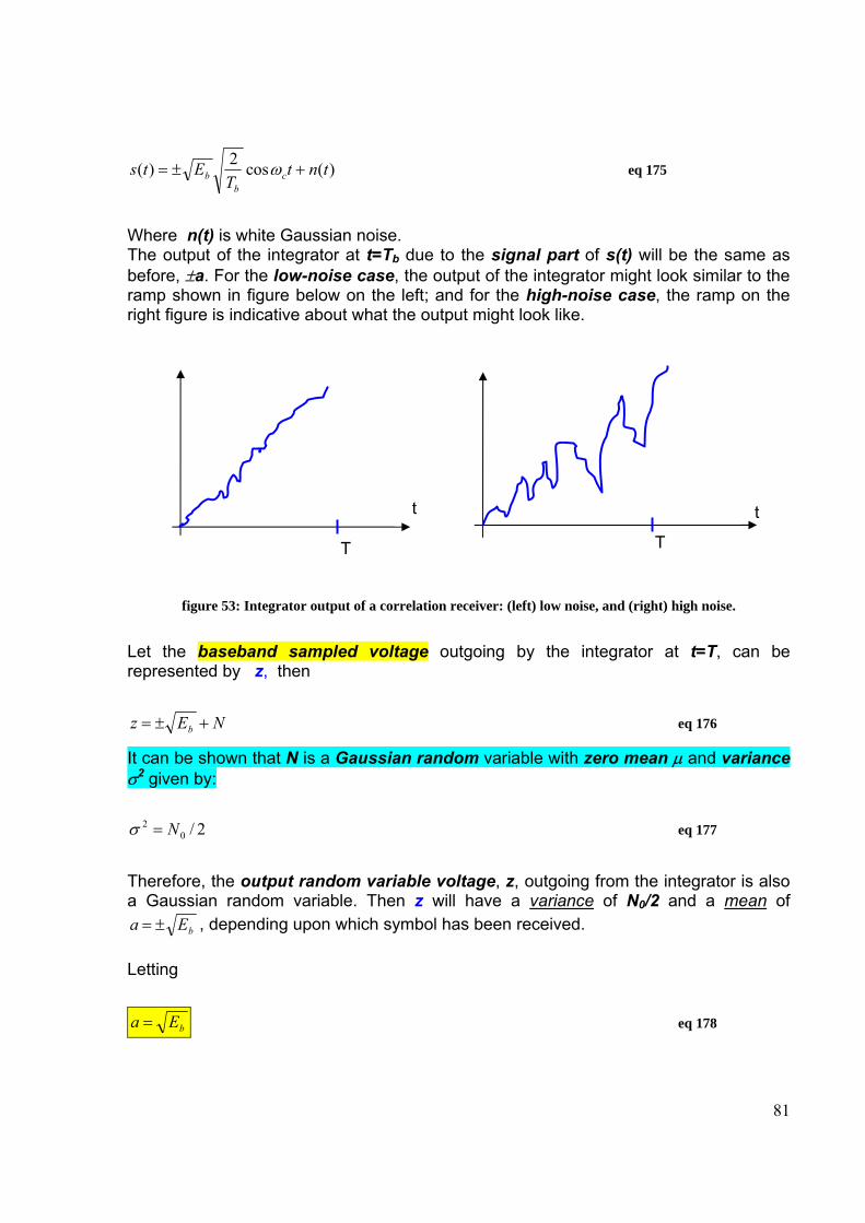
81
)(cos2)( tntT
Ets cb
b +±= ω eq 175
Where n(t) is white Gaussian noise. The output of the integrator at t=Tb due to the signal part of s(t) will be the same as before, ±a. For the low-noise case, the output of the integrator might look similar to the ramp shown in figure below on the left; and for the high-noise case, the ramp on the right figure is indicative about what the output might look like.
figure 53: Integrator output of a correlation receiver: (left) low noise, and (right) high noise.
Let the baseband sampled voltage outgoing by the integrator at t=T, can be represented by z, then
NEz b +±= eq 176
It can be shown that N is a Gaussian random variable with zero mean µ and variance σ2 given by:
2/02 N=σ eq 177
Therefore, the output random variable voltage, z, outgoing from the integrator is also a Gaussian random variable. Then z will have a variance of N0/2 and a mean of
bEa ±= , depending upon which symbol has been received. Letting
bEa = eq 178
T T
t t
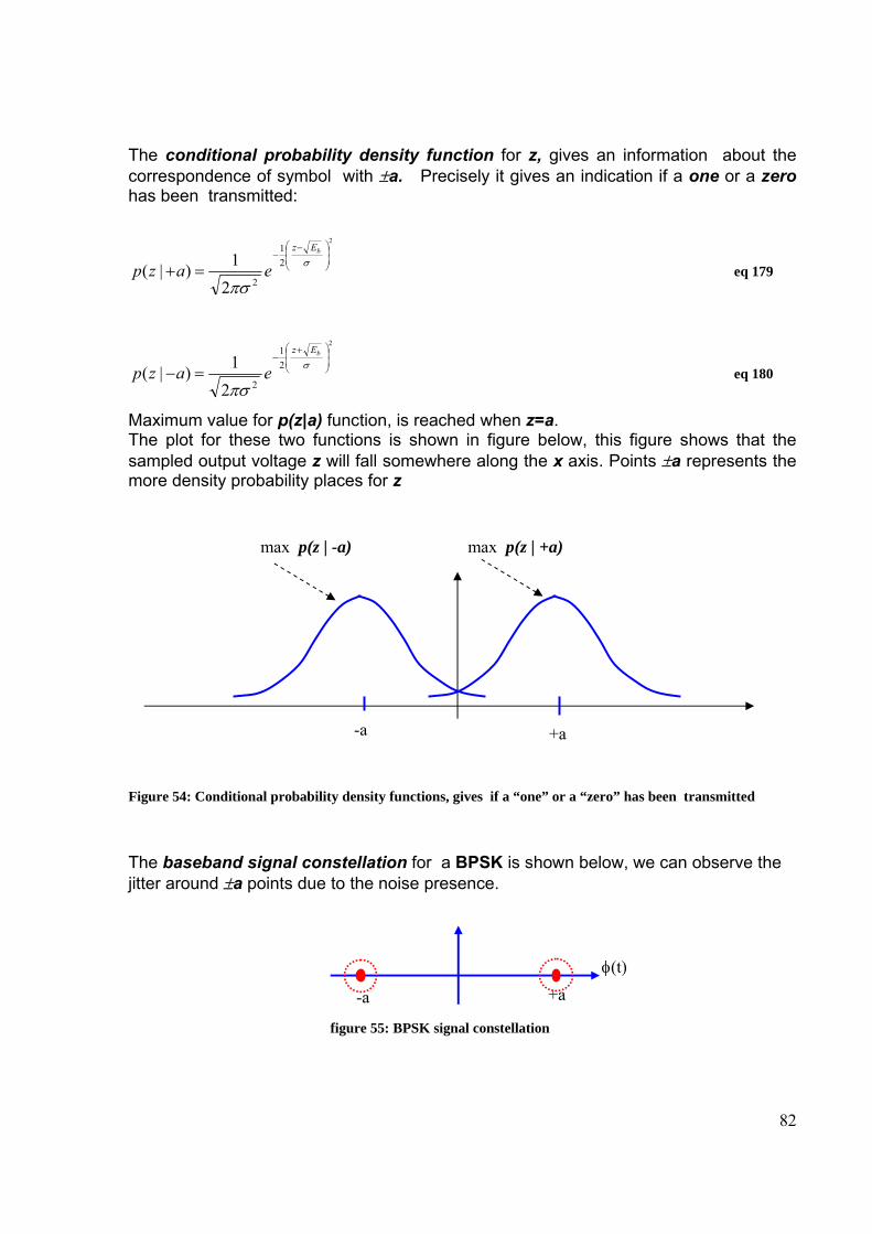
82
The conditional probability density function for z, gives an information about the correspondence of symbol with ±a. Precisely it gives an indication if a one or a zero has been transmitted:
2
21
221)|(
⎟⎟⎠
⎞⎜⎜⎝
⎛ −−
=+ σ
πσ
bEz
eazp eq 179
2
21
221)|(
⎟⎟⎠
⎞⎜⎜⎝
⎛ +−
=− σ
πσ
bEz
eazp eq 180
Maximum value for p(z|a) function, is reached when z=a. The plot for these two functions is shown in figure below, this figure shows that the sampled output voltage z will fall somewhere along the x axis. Points ±a represents the more density probability places for z
Figure 54: Conditional probability density functions, gives if a “one” or a “zero” has been transmitted
The baseband signal constellation for a BPSK is shown below, we can observe the jitter around ±a points due to the noise presence.
figure 55: BPSK signal constellation
max p(z | -a) max p(z | +a)
+a -a
-a +a φ(t)
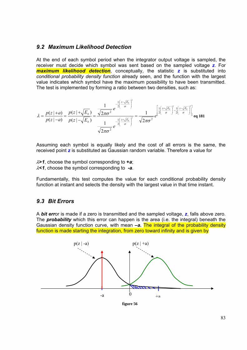
83
9.2 Maximum Likelihood Detection At the end of each symbol period when the integrator output voltage is sampled, the receiver must decide which symbol was sent based on the sampled voltage z. For maximum likelihood detection, conceptually, the statistic z is substituted into conditional probability density function already seen, and the function with the largest value indicates which symbol have the maximum possibility to have been transmitted. The test is implemented by forming a ratio between two densities, such as:
⎥⎥⎥
⎦
⎤
⎢⎢⎢
⎣
⎡
⎟⎟⎠
⎞⎜⎜⎝
⎛ −−⎟
⎟⎠
⎞⎜⎜⎝
⎛ +
⎟⎟⎠
⎞⎜⎜⎝
⎛ +−
⎟⎟⎠
⎞⎜⎜⎝
⎛ −−
==−
+=
−+
=
22
2
2
21
21
2
21
2
21
2
21
21
21
)|()|(
)|()|( σσ
σ
σ
πσ
πσ
πσλbb
b
b
EzEz
Ez
Ez
b
b e
e
e
EzpEzp
azpazp
eq 181
Assuming each symbol is equally likely and the cost of all errors is the same, the received point z is substituted as Gaussian random variable. Therefore a value for λ>1, choose the symbol corresponding to +a; λ<1, choose the symbol corresponding to -a. Fundamentally, this test computes the value for each conditional probability density function at instant and selects the density with the largest value in that time instant.
9.3 Bit Errors A bit error is made if a zero is transmitted and the sampled voltage, z, falls above zero. The probability which this error can happen is the area (i.e. the integral) beneath the Gaussian density function curve, with mean –a. The integral of the probability density function is made starting the integration, from zero toward infinity and is given by
figure 56
p(z | -a) p(z | +a)
+a-a 0
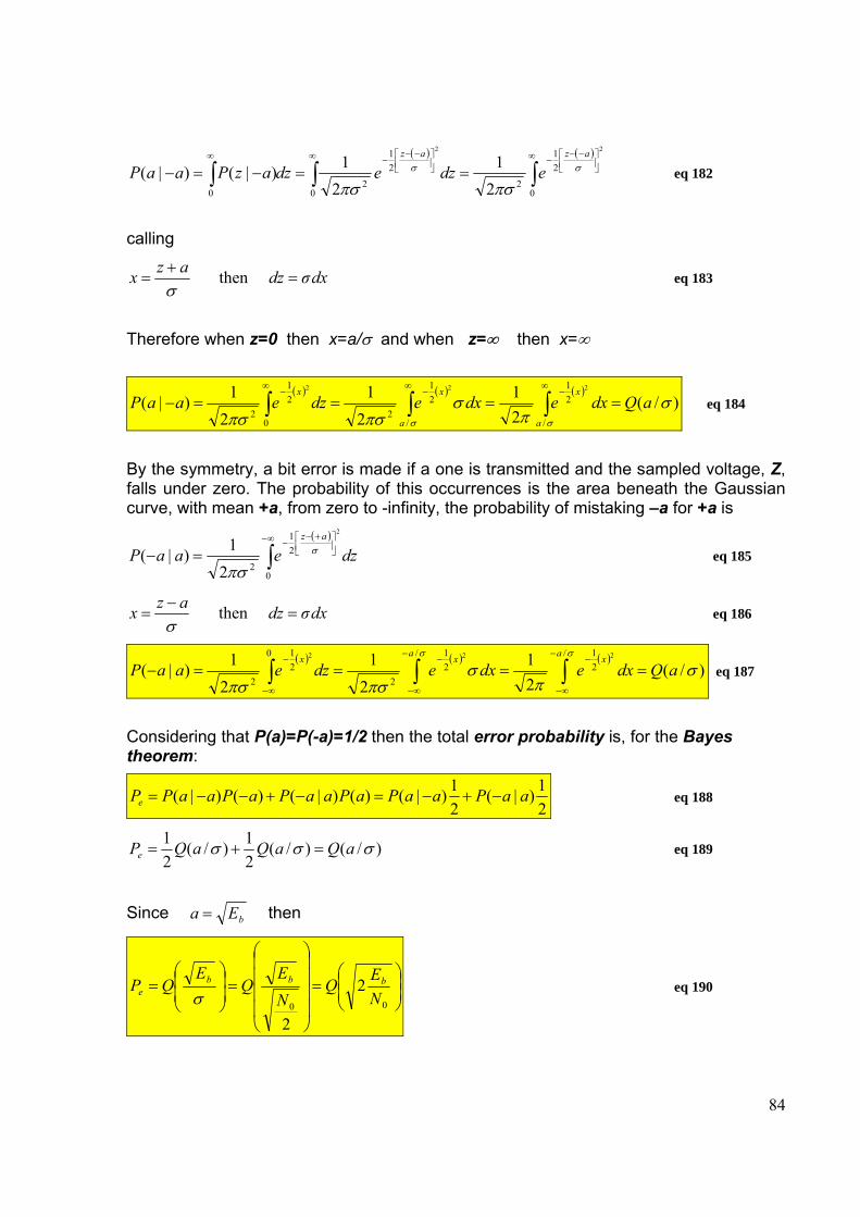
84
( ) ( )
∫∫∫∞
⎥⎦⎤
⎢⎣⎡ −−
−∞⎥⎦⎤
⎢⎣⎡ −−
−∞
==−=−0
21
20
21
20
22
21
21)|()|( σσ
πσπσ
azaz
edzedzazPaaP eq 182
calling
dxσdzazx =+
= n theσ
eq 183
Therefore when z=0 then x=a/σ and when z=∞ then x=∞
( ) ( ) ( ))/(
21
21
21)|(
/
21
/
21
20
21
2
222
σπ
σπσπσ σσ
aQdxedxedzeaaPa
x
a
xx====− ∫∫∫
∞−
∞−
∞−
eq 184
By the symmetry, a bit error is made if a one is transmitted and the sampled voltage, Z, falls under zero. The probability of this occurrences is the area beneath the Gaussian curve, with mean +a, from zero to -infinity, the probability of mistaking –a for +a is
( )
dzeaaPaz
∫∞−
⎥⎦⎤
⎢⎣⎡ +−
−=−
0
21
2
2
21)|( σ
πσ eq 185
dxσdzazx =−
= n theσ
eq 186
( ) ( ) ( ))/(
21
21
21)|(
/21/
21
2
021
2
222
σπ
σπσπσ
σσ
aQdxedxedzeaaPa xa xx
====− ∫∫∫−
∞−
−−
∞−
−
∞−
− eq 187
Considering that P(a)=P(-a)=1/2 then the total error probability is, for the Bayes theorem:
21)|(
21)|()()|()()|( aaPaaPaPaaPaPaaPPe −+−=−+−−= eq 188
)/()/(21)/(
21 σσσ aQaQaQPe =+= eq 189
Since bEa = then
⎟⎟⎠
⎞⎜⎜⎝
⎛=
⎟⎟⎟⎟
⎠
⎞
⎜⎜⎜⎜
⎝
⎛
=⎟⎟⎠
⎞⎜⎜⎝
⎛=
00
2
2NEQ
NE
QE
QP bbbe σ
eq 190
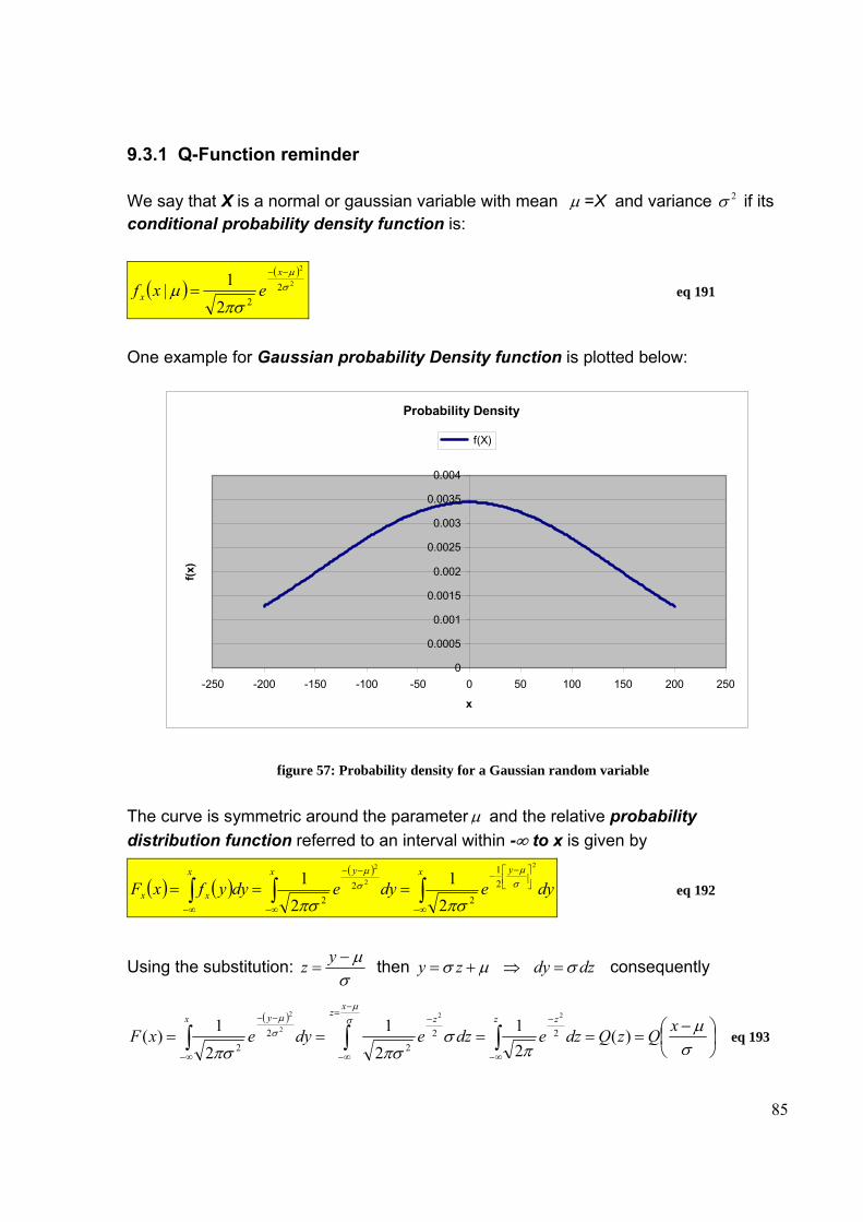
85
9.3.1 Q-Function reminder We say that X is a normal or gaussian variable with mean µ =X and variance 2σ if its conditional probability density function is:
( )( )
2
2
222
1| σµ
πσµ
−−
=x
x exf eq 191
One example for Gaussian probability Density function is plotted below:
Probability Density
0
0.0005
0.001
0.0015
0.002
0.0025
0.003
0.0035
0.004
-250 -200 -150 -100 -50 0 50 100 150 200 250
x
f(x)
f(X)
figure 57: Probability density for a Gaussian random variable
The curve is symmetric around the parameterµ and the relative probability distribution function referred to an interval within -∞ to x is given by
( ) ( )( )
∫∫∫∞−
⎥⎦⎤
⎢⎣⎡ −
−
∞−
−−
∞−
===x yx yx
xx dyedyedyyfxF2
2
2
21
22
2 21
21 σ
µσµ
πσπσ eq 192
Using the substitution: σµ−
=yz then dzdyzy σµσ =⇒+= consequently
( )
⎟⎠⎞
⎜⎝⎛ −
===== ∫∫∫∞−
−−
=
∞−
−
∞−
−−
σµ
πσ
πσπσ
σµ
σµ xQzQdzedzedyexF
z zxz zx y
)(21
21
21)( 22
22
2
22
2
2
eq 193
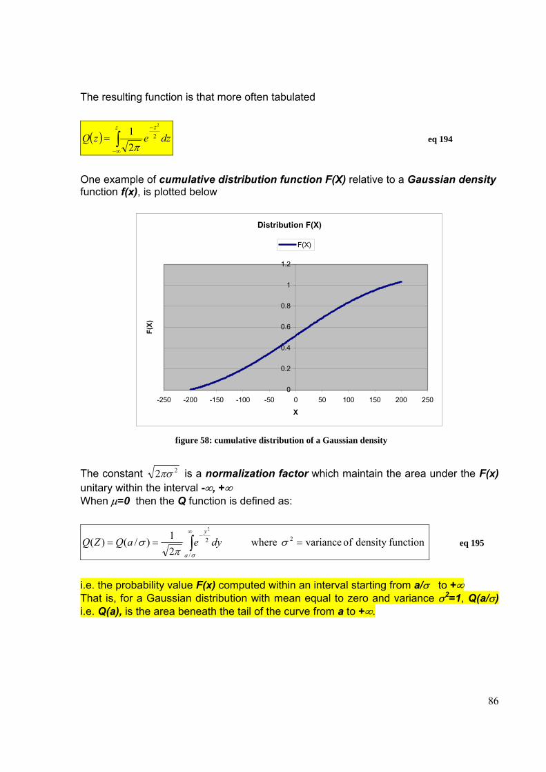
86
The resulting function is that more often tabulated
( ) ∫∞−
−
=z z
dzezQ 2
2
21π
eq 194
One example of cumulative distribution function F(X) relative to a Gaussian density function f(x), is plotted below
Distribution F(X)
0
0.2
0.4
0.6
0.8
1
1.2
-250 -200 -150 -100 -50 0 50 100 150 200 250
X
F(X)
F(X)
figure 58: cumulative distribution of a Gaussian density
The constant 22πσ is a normalization factor which maintain the area under the F(x) unitary within the interval -∞, +∞ When µ=0 then the Q function is defined as:
function density of variance where 21)/()( 2
/
2
2
=== ∫∞
−σ
πσ
σ
dyeaQZQa
y
eq 195
i.e. the probability value F(x) computed within an interval starting from a/σ to +∞ That is, for a Gaussian distribution with mean equal to zero and variance σ2=1, Q(a/σ) i.e. Q(a), is the area beneath the tail of the curve from a to +∞.

87
9.3.2 Bit Error Probability in terms of Eb and N0
Because white noise (AWGN) is presented, it can be shown that the variance of the noise is given by
202 N
=σ eq 196
• N0 = one-sided power spectral density (PSD) of the white noise going into the
IF bandwidth measured in [W/Hz]. Calling:
• Eb= bit energy [J] Eb is a variable that occurs in the theoretical analysis of digital systems, but it is equivalent to the carrier power, C, at the receiver that is measured or determined by link analysis ad is a function of antenna gain, path loss distance. transmitted power, and losses.
bbb R
CTCE == eq 197
Where:
• Tb = bit period = 1/Rb where Rb = bit rate [bit/s] • C = carrier power at the receiver [W] • BIF= bandwidth of the IF [Hz]
The noise power within the IF bandwidth is
IFp BNN 0= eq 198
These parameters can be related as follows:
IF
bb
IF
bb
p BR
NE
BNRE
NC
00
== eq 199
The greater the Rb, the greater the C/Np needed at the receiver side, whereas the greater the bandwidth B, the lower will be the S/N ratio required.
88
C/Np is the carrier-to-noise ratio in the IF, which is determined by link analysis, the BER may be predicted based on this engineering parameter. Consequently :
b
IF
p
b
RB
NC
NE
=0
eq 200
Under the ideal condition and NRZ data format, the assumption is that BIF ≅ Rb ( this is usually not the case unless raised cosine filtering is used); In fact using a RRC filter the since for a BPSK the Symbol rate D is equal to the bit rate Rb, then we can write:
1 when )1(2
)1(2
→≈+=+= rRbrRbrDB eq 201
then the remaining relationship is
p
b
NC
NE
≅0
eq 202
Then using the above relationship, the error probability Pe (BER) may be written as
⎟⎟⎠
⎞⎜⎜⎝
⎛≅⎟
⎟⎠
⎞⎜⎜⎝
⎛=
⎟⎟⎟⎟
⎠
⎞
⎜⎜⎜⎜
⎝
⎛
=⎟⎟⎠
⎞⎜⎜⎝
⎛=
p
bbbe N
CQNEQ
NEQ
EQP 22
200σ
eq 203
This is an important equation that relates the BER to the carrier-to-noise ratio, (C/Np) in the IF bandwidth, which is determined by link analysis.
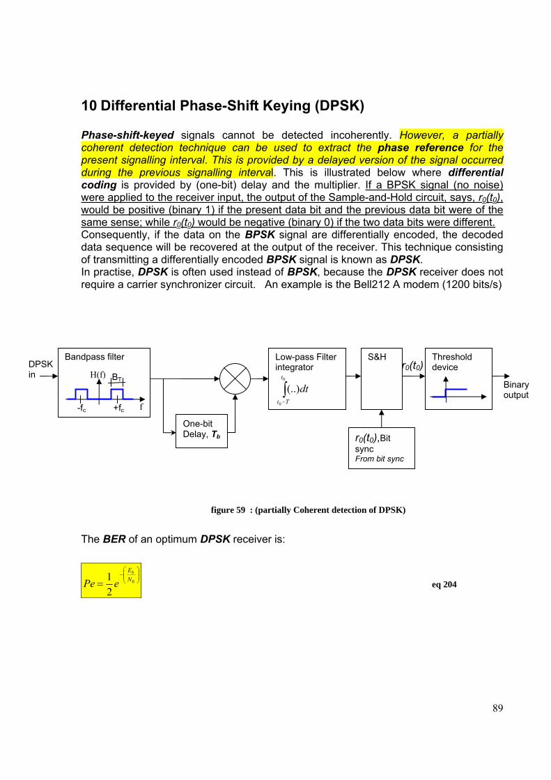
89
10 Differential Phase-Shift Keying (DPSK) Phase-shift-keyed signals cannot be detected incoherently. However, a partially coherent detection technique can be used to extract the phase reference for the present signalling interval. This is provided by a delayed version of the signal occurred during the previous signalling interval. This is illustrated below where differential coding is provided by (one-bit) delay and the multiplier. If a BPSK signal (no noise) were applied to the receiver input, the output of the Sample-and-Hold circuit, says, r0(t0), would be positive (binary 1) if the present data bit and the previous data bit were of the same sense; while r0(t0) would be negative (binary 0) if the two data bits were different. Consequently, if the data on the BPSK signal are differentially encoded, the decoded data sequence will be recovered at the output of the receiver. This technique consisting of transmitting a differentially encoded BPSK signal is known as DPSK. In practise, DPSK is often used instead of BPSK, because the DPSK receiver does not require a carrier synchronizer circuit. An example is the Bell212 A modem (1200 bits/s)
figure 59 : (partially Coherent detection of DPSK)
The BER of an optimum DPSK receiver is:
⎟⎟⎠
⎞⎜⎜⎝
⎛−
= 0
21 N
Eb
ePe eq 204
Threshold device
DPSK in
Low-pass Filter integrator
∫−
0
0
(..)t
Tt
dt
One-bit Delay, Tb
S&H
Bandpass filter
-fc +fc
H(f) BT
f
r0(t0),Bit sync From bit sync i it
r0(t0)
Binary output
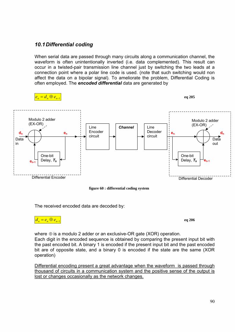
90
10.1 Differential coding When serial data are passed through many circuits along a communication channel, the waveform is often unintentionally inverted (i.e. data complemented). This result can occur in a twisted-pair transmission line channel just by switching the two leads at a connection point where a polar line code is used. (note that such switching would non affect the data on a bipolar signal). To ameliorate the problem, Differential Coding is often employed. The encoded differential data are generated by
1−⊕= nnn ede eq 205
figure 60 : differential coding system
The received encoded data are decoded by:
1−⊕= nnn eed eq 206
where ⊕ is a modulo 2 adder or an exclusive-OR gate (XOR) operation. Each digit in the encoded sequence is obtained by comparing the present input bit with the past encoded bit. A binary 1 is encoded if the present input bit and the past encoded bit are of opposite state, and a binary 0 is encoded if the state are the same (XOR operation) Differential encoding present a great advantage when the waveform is passed through thousand of circuits in a communication system and the positive sense of the output is lost or changes occasionally as the network changes.
One-bit Delay, Tb
Line Encoder circuit
Differential Encoder
Data out
One-bit Delay, Tb
Data in
en-1
en dn
Modulo 2 adder (EX-OR)
Channel Line Decoder circuit
Modulo 2 adder (EX-OR)
Differential Decoder
dn en
en-1
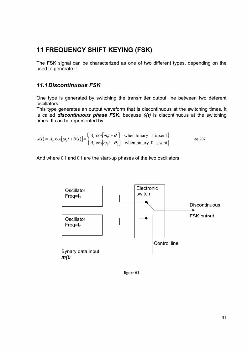
91
11 FREQUENCY SHIFT KEYING (FSK) The FSK signal can be characterized as one of two different types, depending on the used to generate it.
11.1 Discontinuous FSK One type is generated by switching the transmitter output line between two deferent oscillators. This type generates an output waveform that is discontinuous at the switching times, it is called discontinuous phase FSK, because θ(t) is discontinuous at the switching times. It can be represented by:
[ ] [ ][ ] ⎭
⎬⎫
⎩⎨⎧
++
=+=sent is 0binary when cossent is 1binary when cos
)(cos)(22
11
θωθω
θωtAtA
ttAtsc
ccc eq 207
And where θ1 and θ1 are the start-up phases of the two oscillators.
figure 61
Oscillator Freq=f1
Oscillator Freq=f2
Bynary data input m(t)
Control line
Electronic switch
Discontinuous FSK output
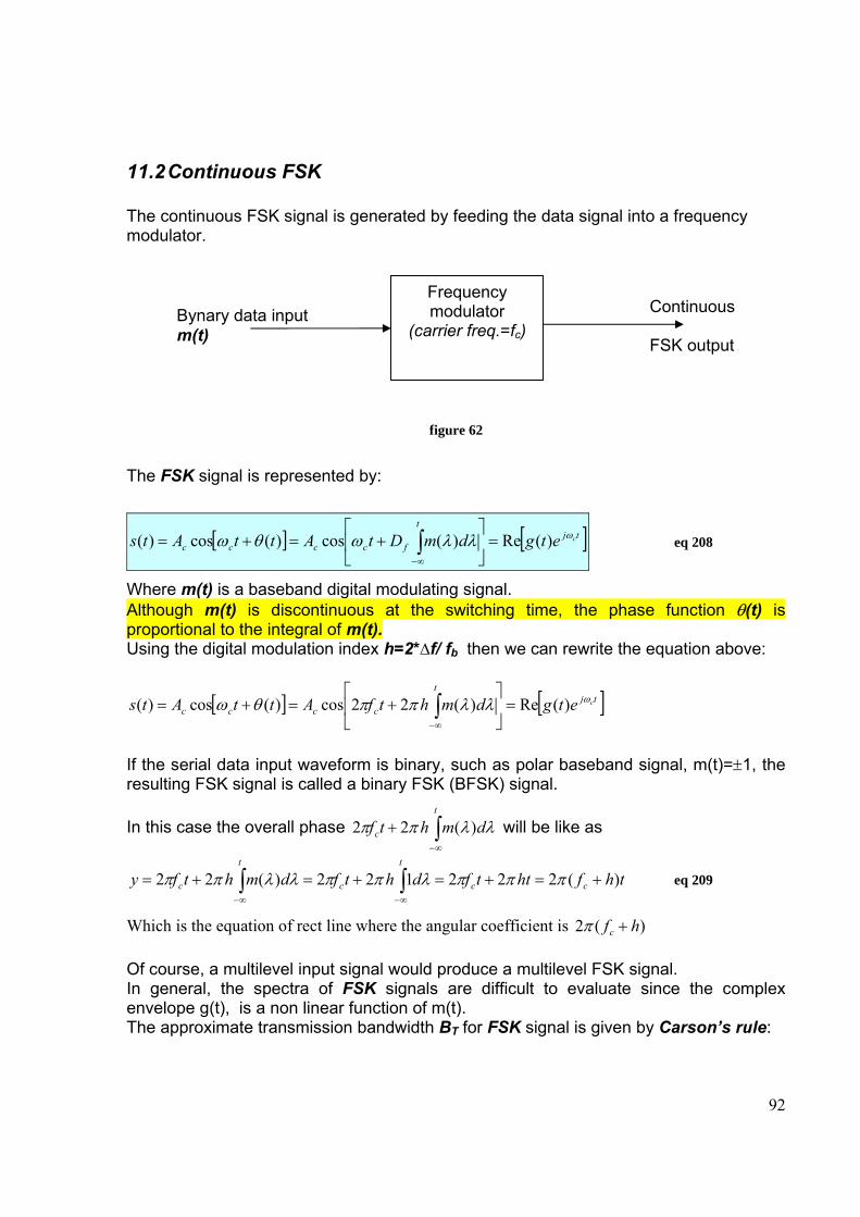
92
11.2 Continuous FSK The continuous FSK signal is generated by feeding the data signal into a frequency modulator.
figure 62
The FSK signal is represented by:
[ ] [ ]tjt
fcccccetgdmDtAttAts ωλλωθω )(Re)(cos)(cos)( =⎥
⎦
⎤⎢⎣
⎡+=+= ∫
∞−
eq 208
Where m(t) is a baseband digital modulating signal. Although m(t) is discontinuous at the switching time, the phase function θ(t) is proportional to the integral of m(t). Using the digital modulation index h=2*∆f/ fb then we can rewrite the equation above:
[ ] [ ]tjt
cccccetgdmhtfAttAts ωλλππθω )(Re)(22cos)(cos)( =⎥
⎦
⎤⎢⎣
⎡+=+= ∫
∞−
If the serial data input waveform is binary, such as polar baseband signal, m(t)=±1, the resulting FSK signal is called a binary FSK (BFSK) signal.
In this case the overall phase ∫∞−
+t
c dmhtf λλππ )(22 will be like as
thfhttfdhtfdmhtfy cc
t
c
t
c )(222122)(22 +=+=+=+= ∫∫∞−∞−
πππλππλλππ eq 209
Which is the equation of rect line where the angular coefficient is )(2 hfc +π Of course, a multilevel input signal would produce a multilevel FSK signal. In general, the spectra of FSK signals are difficult to evaluate since the complex envelope g(t), is a non linear function of m(t). The approximate transmission bandwidth BT for FSK signal is given by Carson’s rule:
Bynary data input m(t)
Frequency modulator
(carrier freq.=fc) Continuous FSK output
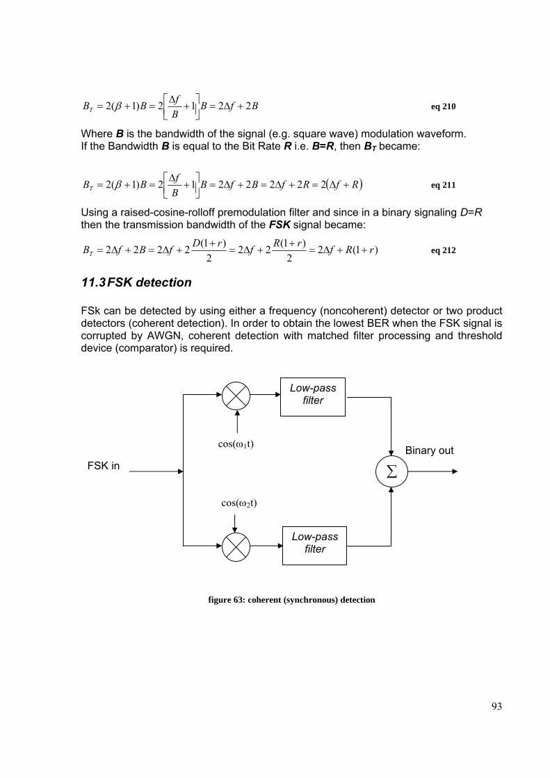
93
BfBBfBBT 2212)1(2 +∆=⎥⎦
⎤⎢⎣⎡ +∆
=+= β eq 210
Where B is the bandwidth of the signal (e.g. square wave) modulation waveform. If the Bandwidth B is equal to the Bit Rate R i.e. B=R, then BT became:
( )RfRfBfBBfBBT +∆=+∆=+∆=⎥⎦
⎤⎢⎣⎡ +∆
=+= 2222212)1(2 β eq 211
Using a raised-cosine-rolloff premodulation filter and since in a binary signaling D=R then the transmission bandwidth of the FSK signal became:
)1(22
)1(222
)1(2222 rRfrRfrDfBfBT ++∆=+
+∆=+
+∆=+∆= eq 212
11.3 FSK detection FSk can be detected by using either a frequency (noncoherent) detector or two product detectors (coherent detection). In order to obtain the lowest BER when the FSK signal is corrupted by AWGN, coherent detection with matched filter processing and threshold device (comparator) is required.
figure 63: coherent (synchronous) detection
Low-pass filter
cos(ω1t)
FSK in ∑
Low-pass filter
cos(ω2t)
Binary out
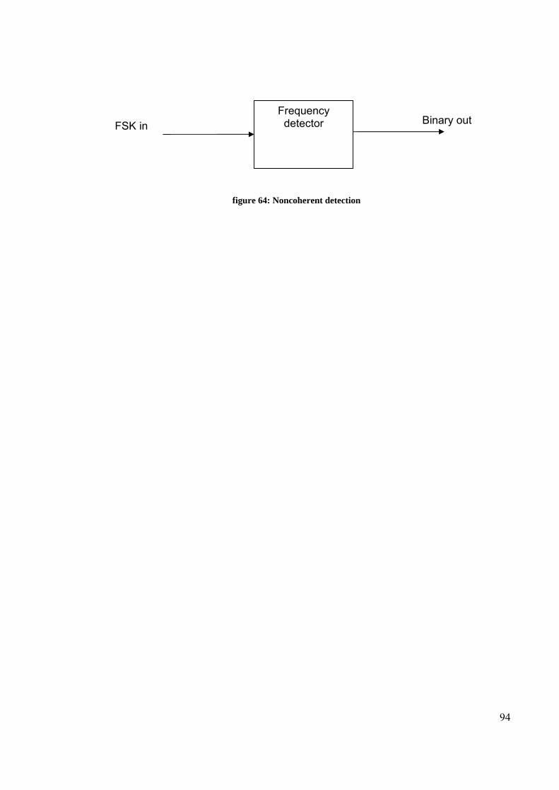
94
figure 64: Noncoherent detection
FSK in Frequency detector Binary out
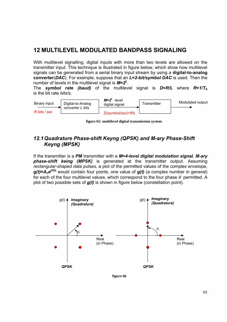
95
12 MULTILEVEL MODULATED BANDPASS SIGNALING With multilevel signalling, digital inputs with more than two levels are allowed on the transmitter input. This technique is illustrated in figure below, which show how multilevel signals can be generated from a serial binary input stream by using a digital-to-analog converter(DAC). For example, suppose that an L=2-bit/symbol DAC is used. Then the number of levels in the multilevel signal is M=2L. The symbol rate (baud) of the multilevel signal is D=R/L where R=1/Tb is the bit rate bits/s.
figure 65: multilevel digital transmission system
12.1 Quadrature Phase-shift Keyng (QPSK) and M-ary Phase-Shift Keyng (MPSK)
If the transmitter is a PM transmitter with a M=4-level digital modulation signal, M-ary phase-shift keing (MPSK) is generated at the transmitter output. Assuming rectangular-shaped data pulses, a plot of the permitted values of the complex envelope, g(t)=Acejθ(t), would contain four points, one value of g(t) (a complex number in general) for each of the four multilevel values, which correspond to the four phase θ permitted. A plot of two possible sets of g(t) is shown in figure below (constellation point).
figure 66
Binary input R bits / sec
Transmitter Modulated output Digital-to-Analog converter L bits
M=2L -level digital signal D(symbol/sec)=R/L
g(t)
Real (in Phase)
Imaginary (Quadrature)
θi
g(t)
Real (in Phase)
Imaginary (Quadrature)
θi
QPSK QPSK
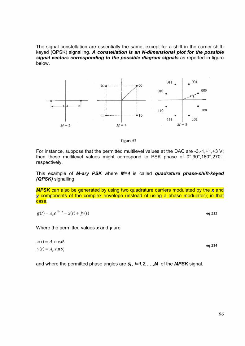
96
The signal constellation are essentially the same, except for a shift in the carrier-shift-keyed (QPSK) signalling. A constellation is an N-dimensional plot for the possible signal vectors corresponding to the possible diagram signals as reported in figure below.
figure 67
For instance, suppose that the permitted multilevel values at the DAC are -3,-1,+1,+3 V; then these multilevel values might correspond to PSK phase of 0°,90°,180°,270°, respectively.
This example of M-ary PSK where M=4 is called quadrature phase-shift-keyed (QPSK) signalling.
MPSK can also be generated by using two quadrature carriers modulated by the x and y components of the complex envelope (instead of using a phase modulator); in that case,
)()()( )( tjytxeAtg tjc +== θ eq 213
Where the permitted values x and y are
ic
ic
AtyAtx
θθ
sin)(cos)(
==
eq 214
and where the permitted phase angles are θI , i=1,2,….,M of the MPSK signal.
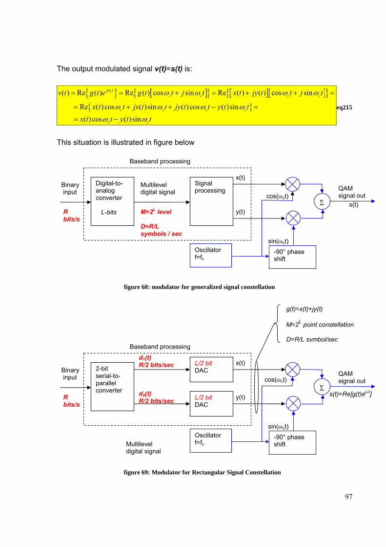
97
The output modulated signal v(t)=s(t) is:
{ } [ ]{ } [ ][ ]{ }{ }
( ) Re ( ) Re ( ) cos sin Re ( ) ( ) cos sin
Re ( )cos ( )sin ( ) cos ( )sin ( ) cos ( )sin
cj tc c c c
c c c c
c c
v t g t e g t t j t x t jy t t j t
x t t jx t t jy t t y t tx t t y t t
ω ω ω ω ω
ω ω ω ω
ω ω
= = + = + + =
= + + − =
= −
eq215
This situation is illustrated in figure below
figure 68: modulator for generalized signal constellation
figure 69: Modulator for Rectangular Signal Constellation
x(t) Binary input
2-bit serial-to-parallel converter
L/2 bit DAC
R bits/s
Multilevel digital signal
d1(t) R/2 bits/sec
y(t)
cos(ωct)
Oscillator f=fc
Σ
-90° phase shift
sin(ωct)
s(t)=Re[g(t)ejωt]
QAM signal out
Baseband processing
L/2 bit DAC
d2(t) R/2 bits/sec
g(t)=x(t)+jy(t) M=2L point constellation D=R/L symbol/sec
x(t) Binary input
Digital-to-analog converter L-bits
Signal processing
Oscillator f=fc
Σ
-90° phase shift
R bits/s
Multilevel digital signal
M=2L level D=R/L symbols / sec
y(t)
cos(ωct)
sin(ωct)
s(t)
QAM signal out
Baseband processing
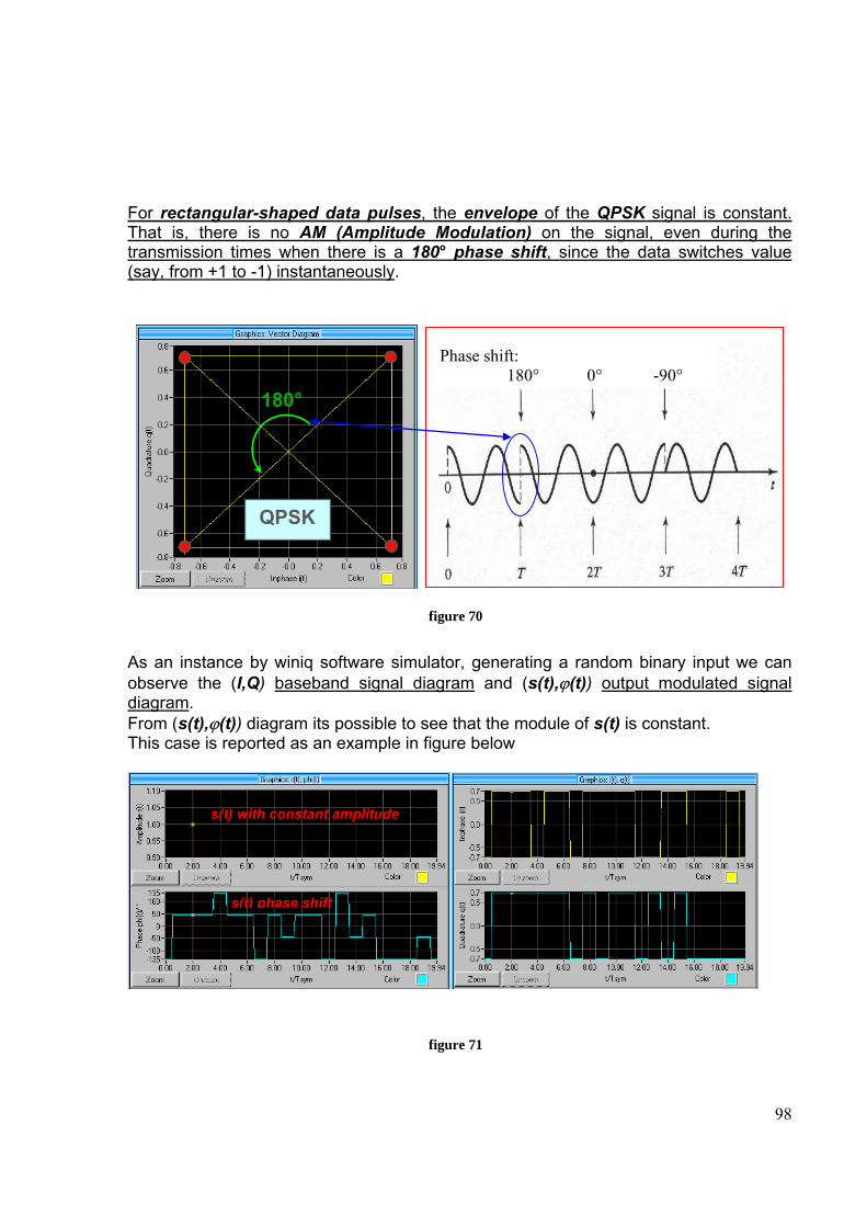
98
For rectangular-shaped data pulses, the envelope of the QPSK signal is constant. That is, there is no AM (Amplitude Modulation) on the signal, even during the transmission times when there is a 180° phase shift, since the data switches value (say, from +1 to -1) instantaneously.
figure 70
As an instance by winiq software simulator, generating a random binary input we can observe the (I,Q) baseband signal diagram and (s(t),ϕ(t)) output modulated signal diagram. From (s(t),ϕ(t)) diagram its possible to see that the module of s(t) is constant. This case is reported as an example in figure below
figure 71
QPSK
180°
Phase shift: 180° 0° -90°
s(t) with constant amplitude
s(t) phase shift
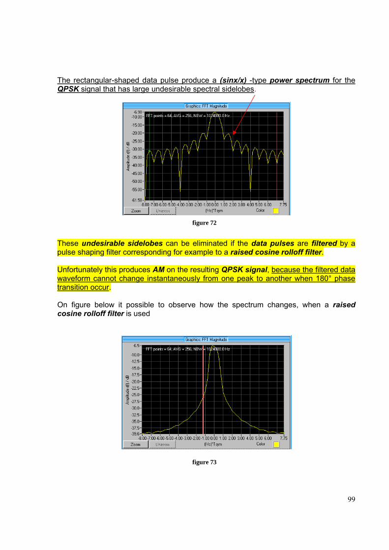
99
The rectangular-shaped data pulse produce a (sinx/x) -type power spectrum for the QPSK signal that has large undesirable spectral sidelobes.
figure 72
These undesirable sidelobes can be eliminated if the data pulses are filtered by a pulse shaping filter corresponding for example to a raised cosine rolloff filter. Unfortunately this produces AM on the resulting QPSK signal, because the filtered data waveform cannot change instantaneously from one peak to another when 180° phase transition occur. On figure below it possible to observe how the spectrum changes, when a raised cosine rolloff filter is used
figure 73
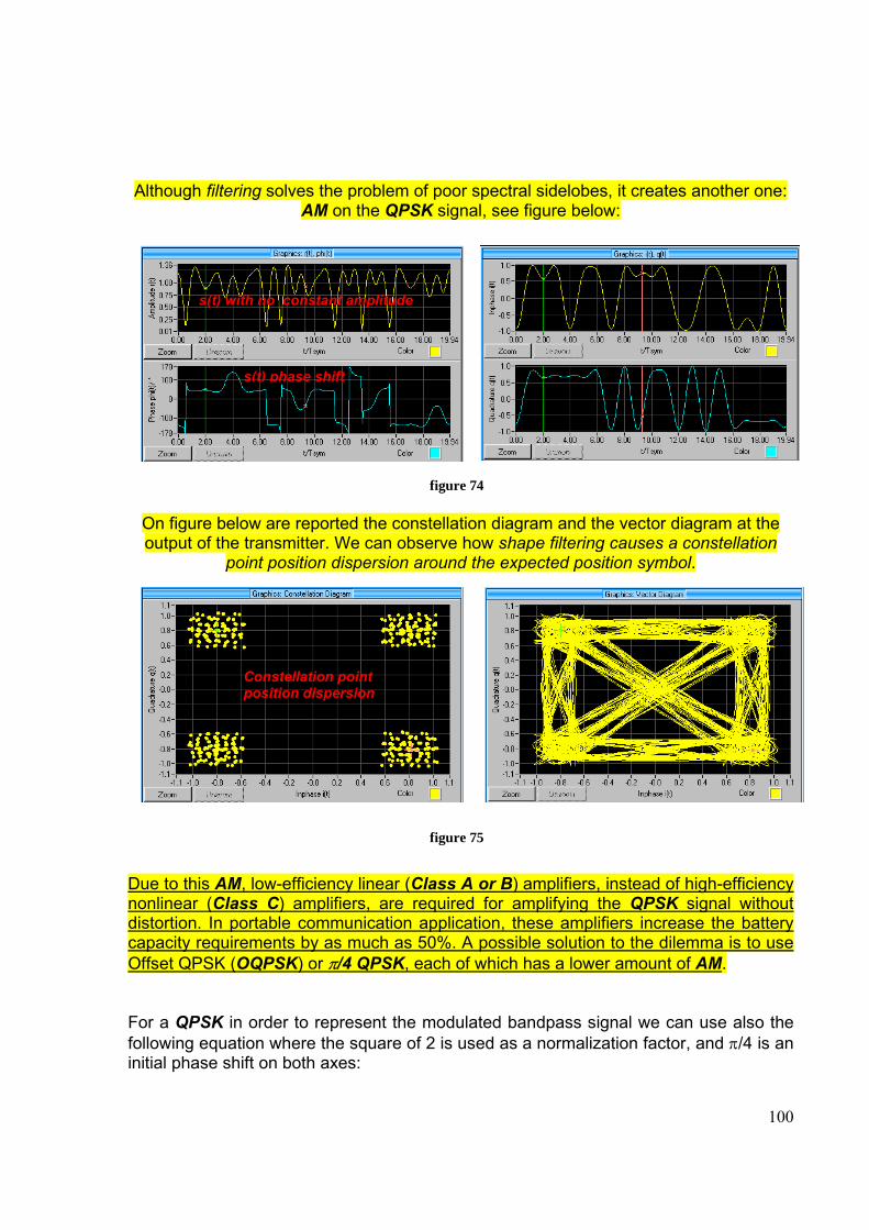
100
Although filtering solves the problem of poor spectral sidelobes, it creates another one: AM on the QPSK signal, see figure below:
figure 74
On figure below are reported the constellation diagram and the vector diagram at the output of the transmitter. We can observe how shape filtering causes a constellation
point position dispersion around the expected position symbol.
figure 75
Due to this AM, low-efficiency linear (Class A or B) amplifiers, instead of high-efficiency nonlinear (Class C) amplifiers, are required for amplifying the QPSK signal without distortion. In portable communication application, these amplifiers increase the battery capacity requirements by as much as 50%. A possible solution to the dilemma is to use Offset QPSK (OQPSK) or π/4 QPSK, each of which has a lower amount of AM. For a QPSK in order to represent the modulated bandpass signal we can use also the following equation where the square of 2 is used as a normalization factor, and π/4 is an initial phase shift on both axes:
s(t) with no constant amplitude
s(t) phase shift
Constellation point position dispersion
101
)4
2sin()(2
1)4
2cos()(2
1)](2cos[)( ππππθπ +++=+= tftdtftdttfts cQcIc
Where
)......(,,)......(,,
531
420
oddbitddddevenbitdddd
Q
I
==
figure 76
In other word, as we have already seen a QPSK signal can be represented as the superposition of two BPSK signal with carrier in quadrature. Each signal is characterized by a 2Tb symbol time, i.e. double time length with respect to original modulating signal.
102
x(t)
y(t)
cos(ωct)
Oscillator f=fc
Σ
-90° phase shift
sin(ωct)
s(t)=Re[g(t)ejωt]
QAM signal out
g(t)=x(t)+jy(t) M=2l point constellation D=R/l symbol/sec
Ts/2 delay
12.2 OQPSK and π/4 QPSK Offset Quadrature Phase-Shift keying (OQPSK) is M=4 PSK in which the allowed data transition times for I and Q components are offset by ½ symbol (i.e. by 1 bit) interval. This offset provides an advantage when nonrectangular (i.e. filtered) data pulses are used, because the offset greatly reduces the AM on the OQPSK signal compared to the AM on the corresponding QPSK signal. The AM is reduced because a maximum phase transition of only 90° occurs for OQPSK signalling (as opposed to 180° for QPSK), since the I and Q data cannot change simultaneously, because the data are offset.
figure 77
In mathematical form we have:
422 2 === lM eq 216
lR
symbolperbitofnumberBitRate
TratesymbolD
s
====____
1_ eq 217
2_ sTdelaySymbol = eq 218
• in a usual QAM the I and Q component are:
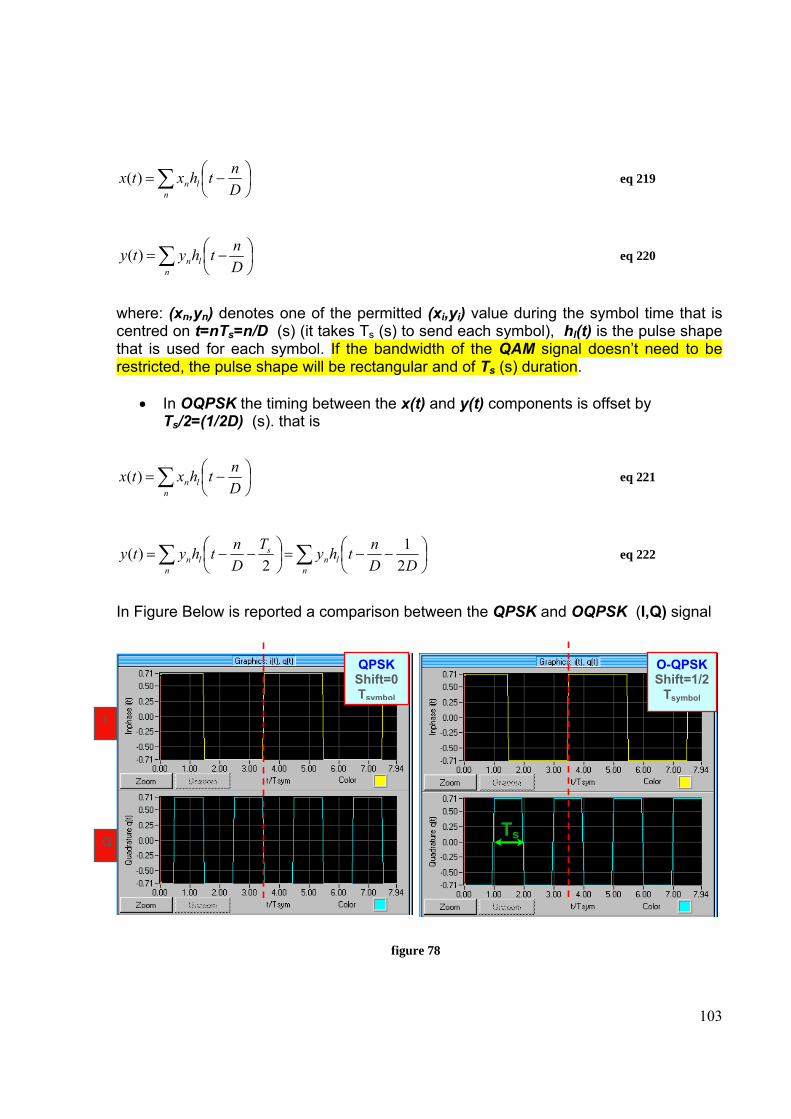
103
∑ ⎟⎠⎞
⎜⎝⎛ −=
nln D
nthxtx )( eq 219
∑ ⎟⎠⎞
⎜⎝⎛ −=
nln D
nthyty )( eq 220
where: (xn,yn) denotes one of the permitted (xi,yi) value during the symbol time that is centred on t=nTs=n/D (s) (it takes Ts (s) to send each symbol), hl(t) is the pulse shape that is used for each symbol. If the bandwidth of the QAM signal doesn’t need to be restricted, the pulse shape will be rectangular and of Ts (s) duration.
• In OQPSK the timing between the x(t) and y(t) components is offset by Ts/2=(1/2D) (s). that is
∑ ⎟⎠⎞
⎜⎝⎛ −=
nln D
nthxtx )( eq 221
∑∑ ⎟⎠⎞
⎜⎝⎛ −−=⎟
⎠⎞
⎜⎝⎛ −−=
nln
n
sln DD
nthyTDnthyty
21
2)( eq 222
In Figure Below is reported a comparison between the QPSK and OQPSK (I,Q) signal
figure 78
O-QPSK Shift=1/2
Tsymbol
QPSK Shift=0 Tsymbol
Ts
I
Q
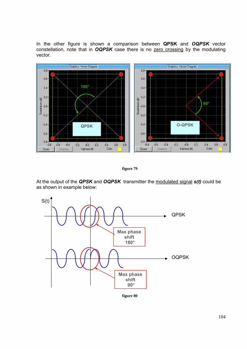
104
In the other figure is shown a comparison between QPSK and OQPSK vector constellation, note that in OQPSK case there is no zero crossing by the modulating vector.
figure 79
At the output of the QPSK and OQPSK transmitter the modulated signal s(t) could be as shown in example below:
figure 80
O-QPSK
90°
QPSK
180°
QPSK
S(t)
OQPSK
Max phase shift 180°
Max phase shift 90°
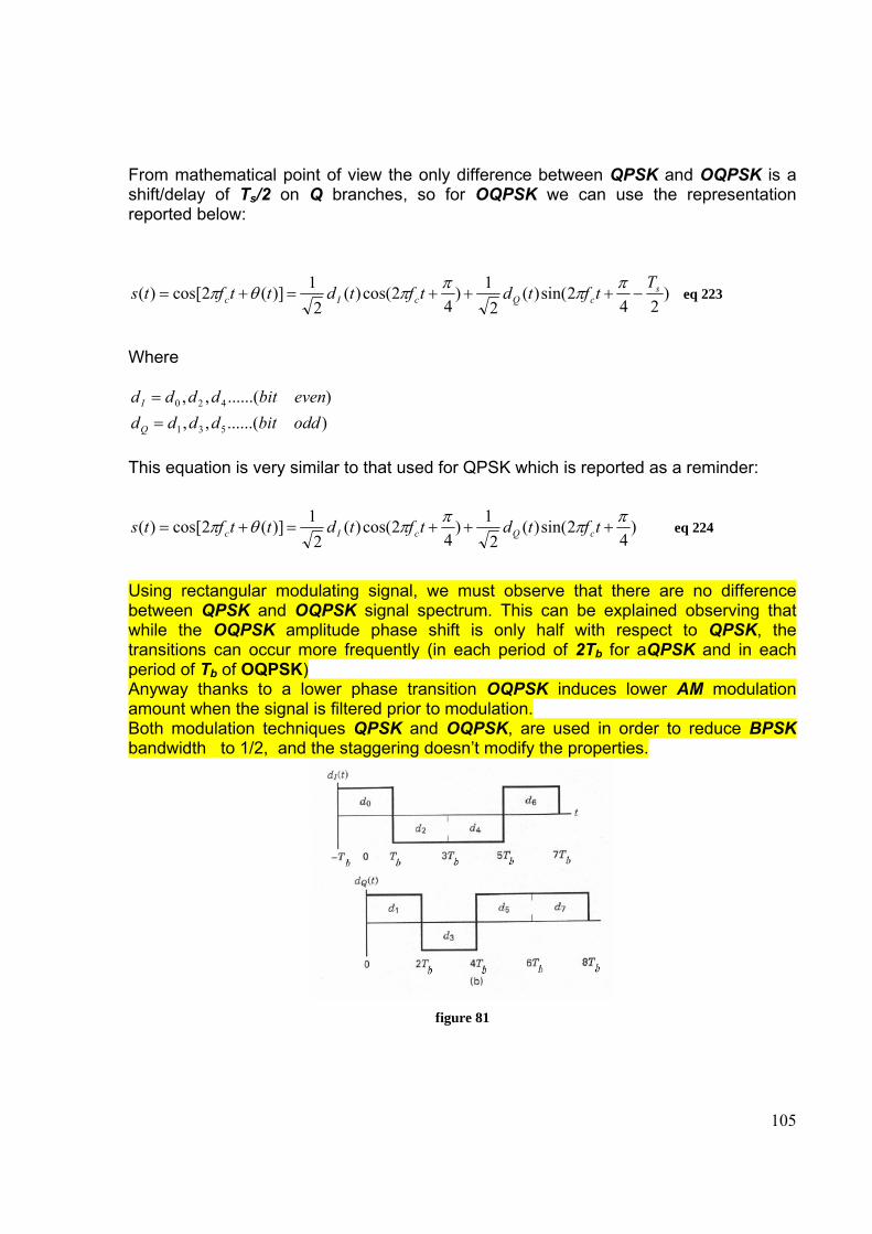
105
From mathematical point of view the only difference between QPSK and OQPSK is a shift/delay of Ts/2 on Q branches, so for OQPSK we can use the representation reported below:
)24
2sin()(2
1)4
2cos()(2
1)](2cos[)( scQcIc
Ttftdtftdttfts −+++=+=ππππθπ eq 223
Where
)......(,,)......(,,
531
420
oddbitddddevenbitdddd
Q
I
==
This equation is very similar to that used for QPSK which is reported as a reminder:
)4
2sin()(2
1)4
2cos()(2
1)](2cos[)( ππππθπ +++=+= tftdtftdttfts cQcIc eq 224
Using rectangular modulating signal, we must observe that there are no difference between QPSK and OQPSK signal spectrum. This can be explained observing that while the OQPSK amplitude phase shift is only half with respect to QPSK, the transitions can occur more frequently (in each period of 2Tb for aQPSK and in each period of Tb of OQPSK) Anyway thanks to a lower phase transition OQPSK induces lower AM modulation amount when the signal is filtered prior to modulation. Both modulation techniques QPSK and OQPSK, are used in order to reduce BPSK bandwidth to 1/2, and the staggering doesn’t modify the properties.
figure 81
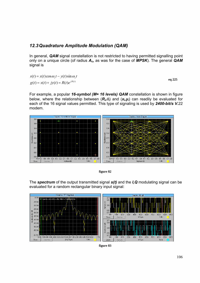
106
12.3 Quadrature Amplitude Modulation (QAM) In general, QAM signal constellation is not restricted to having permitted signalling point only on a unique circle (of radius Ac, as was for the case of MPSK). The general QAM signal is
)()()()()(
sin)(cos)()(tj
cc
etRtjytxtg
ttyttxtsϑ
ωω
=+=
−= eq 225
For example, a popular 16-symbol (M= 16 levels) QAM constellation is shown in figure below, where the relationship between (Ri,θi) and (xi,yi) can readily be evaluated for each of the 16 signal values permitted. This type of signaling is used by 2400-bit/s V.22 modem.
figure 82
The spectrum of the output transmitted signal s(t) and the I,Q modulating signal can be evaluated for a random rectangular binary input signal:
figure 83
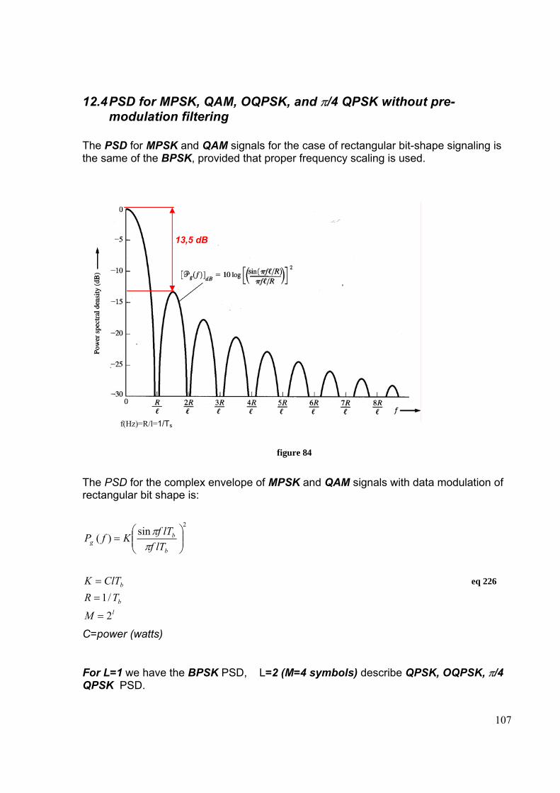
107
12.4 PSD for MPSK, QAM, OQPSK, and π/4 QPSK without pre-modulation filtering
The PSD for MPSK and QAM signals for the case of rectangular bit-shape signaling is the same of the BPSK, provided that proper frequency scaling is used.
figure 84
The PSD for the complex envelope of MPSK and QAM signals with data modulation of rectangular bit shape is:
l
b
b
b
bg
M
TRClTK
lTflTfKfP
2
/1
sin)(2
=
==
⎟⎟⎠
⎞⎜⎜⎝
⎛=
ππ
eq 226
C=power (watts) For L=1 we have the BPSK PSD, L=2 (M=4 symbols) describe QPSK, OQPSK, π/4 QPSK PSD.
13,5 dB
f(Hz)=R/l=1/Ts
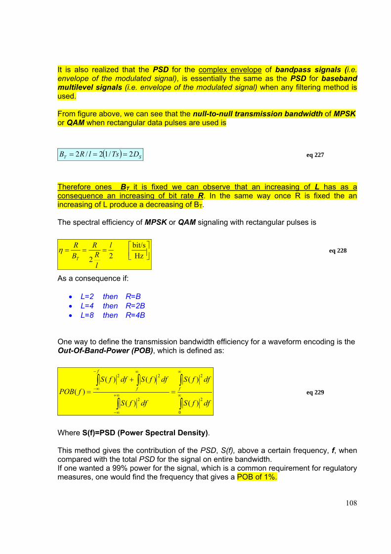
108
It is also realized that the PSD for the complex envelope of bandpass signals (i.e. envelope of the modulated signal), is essentially the same as the PSD for baseband multilevel signals (i.e. envelope of the modulated signal) when any filtering method is used. From figure above, we can see that the null-to-null transmission bandwidth of MPSK or QAM when rectangular data pulses are used is
( ) ST DTslRB 2/12/2 === eq 227
Therefore ones BT it is fixed we can observe that an increasing of L has as a consequence an increasing of bit rate R. In the same way once R is fixed the an increasing of L produce a decreasing of BT. The spectral efficiency of MPSK or QAM signaling with rectangular pulses is
⎥⎦⎤
⎢⎣⎡===
Hzbit/s
22
l
lR
RBR
T
η eq 228
As a consequence if:
• L=2 then R=B • L=4 then R=2B • L=8 then R=4B
One way to define the transmission bandwidth efficiency for a waveform encoding is the Out-Of-Band-Power (POB), which is defined as:
∫
∫
∫
∫ ∫∞
∞
∞+
∞−
−
∞−
∞
=
+
=
0
2
2
2
22
)(
)(
)(
)()()(
dffS
dffS
dffS
dffSdffSfPOB f
f
f eq 229
Where S(f)=PSD (Power Spectral Density). This method gives the contribution of the PSD, S(f), above a certain frequency, f, when compared with the total PSD for the signal on entire bandwidth. If one wanted a 99% power for the signal, which is a common requirement for regulatory measures, one would find the frequency that gives a POB of 1%.
109
12.5 Spectral efficiency for MPSK, QAM,OQPSK, and π/4 QPSK with Raised Cosine Filtering
The spectrum shown above was obtained for the case of rectangular symbol pulses shaping, and the spectral side lobes was terrible. The first side lobe is attenuated only by ≅ 13.5 dB.
figure 85
The high side lobes can be eliminated if raised cosine filtering is used (since the raised cosine filter has an absolutely band limited frequency response). We should select the 6-dB bandwidth f0 of the raised cosine filter, for the baseband signal, equal to half of the symbol (baud) rate in order for o avoid ISI. That is
sTlRDf 1
21
21
21
0 === eq 230
In practise, a square root raised cosine SRRC frequency response characteristic is often used at the transmitter, along with another SRRC filter at the receiver, in order to simultaneously prevent ISI on the received filtered pulses and minimize the bit errors due to channel noise. However the SRRC filter also introduces AM on the transmitted signal. If the overall pulse shape satisfies the raised cosine-rolloff filter characteristic, then, the absolute bandwidth of the M-level modulating baseband signal signal is
13,5 dB
110
( )[ ]
symbol/s 12
or
Hz 121
lR
rBD
DrB
=⎟⎠⎞
⎜⎝⎛+
=
+=
eq 231
r is the characteristic of the filter called rolloff factor. From AM study modulation we know that the transmission bandwidth BT is related to the modulation bandwidth B by
BBT 2= eq 232
so the overall absolute transmission bandwidth of the QAM signal with raised cosine filtered pulses is:
( )[ ] ( )[ ] ( ) Hz 11 12122 ⎥⎦
⎤⎢⎣⎡ +=+=+==
lRrDrDrBBT eq 233
This bandwidth can be compared to a null bandwidth lRBT 2= of rectangular pulse
shaping i.e. without SRRC filter). We can see that the greeter the r , the greeter the BT, when r=1 then we have again the maximum bandwidth such as we used the rectangular filter shape. On table below are reported some values of the parameter related to the above equations supposing a fixed bit-rate R=812 Kbit/s. Note that when the rolloff factor of the SRRC filter tend to 1 then the bandwidth BT become the same as found for rectangular filter data pulse shape.
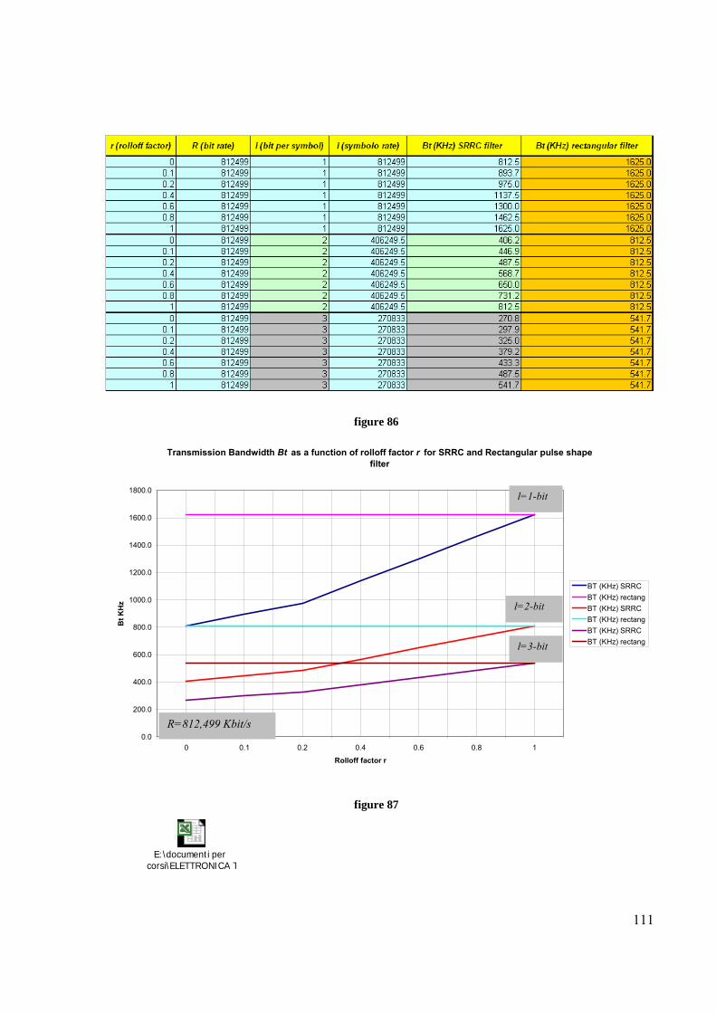
111
Transmission Bandwidth Bt as a function of rolloff factor r for SRRC and Rectangular pulse shape filter
0.0
200.0
400.0
600.0
800.0
1000.0
1200.0
1400.0
1600.0
1800.0
0 0.1 0.2 0.4 0.6 0.8 1
Rolloff factor r
Bt K
Hz
BT (KHz) SRRCBT (KHz) rectangBT (KHz) SRRCBT (KHz) rectangBT (KHz) SRRCBT (KHz) rectang
l=1-bit
l=2-bit
l=3-bit
R=812,499 Kbit/s
figure 86
figure 87
E:\documenti per corsi\ELETTRONICA T
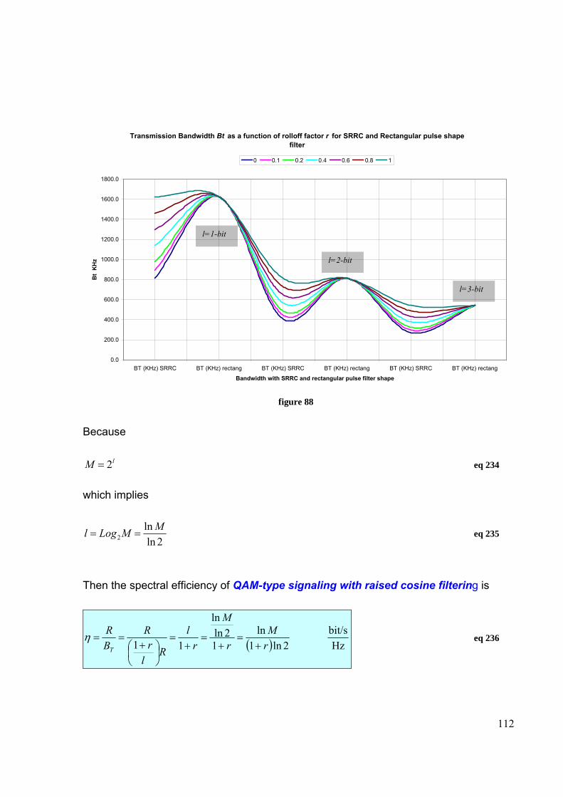
112
l=1-bit
l=2-bit
l=3-bit
Transmission Bandwidth Bt as a function of rolloff factor r for SRRC and Rectangular pulse shape filter
0.0
200.0
400.0
600.0
800.0
1000.0
1200.0
1400.0
1600.0
1800.0
BT (KHz) SRRC BT (KHz) rectang BT (KHz) SRRC BT (KHz) rectang BT (KHz) SRRC BT (KHz) rectang
Bandwidth with SRRC and rectangular pulse filter shape
Bt
KH
z
0 0.1 0.2 0.4 0.6 0.8 1
figure 88
Because
lM 2= eq 234
which implies
2lnln
2MMLogl == eq 235
Then the spectral efficiency of QAM-type signaling with raised cosine filtering is
( ) Hzbit/s
2ln1ln
12ln
ln
11 rM
r
M
rl
Rl
rR
BR
T +=
+=
+=
⎟⎠⎞
⎜⎝⎛ +
==η eq 236
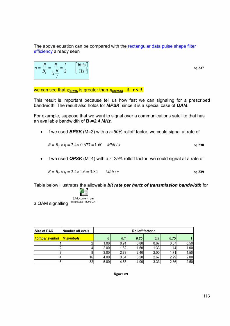
113
The above equation can be compared with the rectangular data pulse shape filter efficiency already seen
⎥⎦⎤
⎢⎣⎡===
Hzbit/s
22
l
lR
RBR
T
η eq 237
we can see that ηSRRC is greater than ηrectang if r < 1. This result is important because tell us how fast we can signaling for a prescribed bandwidth. The result also holds for MPSK, since it is a special case of QAM. For example, suppose that we want to signal over a communications satellite that has an available bandwidth of BT=2.4 MHz.
• If we used BPSK (M=2) with a r=50% rolloff factor, we could signal at rate of
sMbitBR T / 60.1677.04.2 =×=×= η eq 238
• If we used QPSK (M=4) with a r=25% rolloff factor, we could signal at a rate of
sMbitBR T / 84.36.14.2 =×=×= η eq 239
Table below illustrates the allowable bit rate per hertz of transmission bandwidth for
a QAM signalling E:\documenti per
corsi\ELETTRONICA T Size of DAC Number ofLevels
l bit per symbol M symbols 0 0.1 0.25 0.5 0.75 11 2 1.00 0.91 0.80 0.67 0.57 0.502 4 2.00 1.82 1.60 1.33 1.14 1.003 8 3.00 2.73 2.40 2.00 1.71 1.504 16 4.00 3.64 3.20 2.67 2.29 2.005 32 5.00 4.55 4.00 3.33 2.86 2.50
Rolloff factor r
figure 89
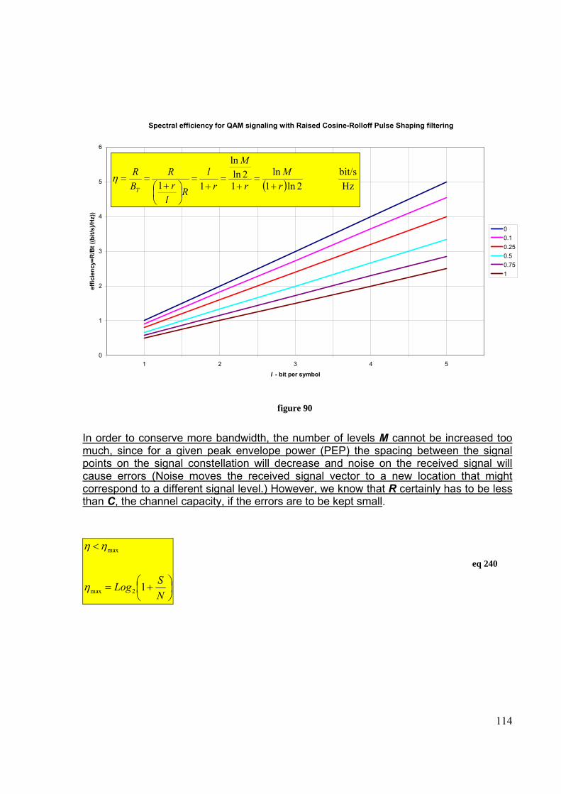
114
Spectral efficiency for QAM signaling with Raised Cosine-Rolloff Pulse Shaping filtering
0
1
2
3
4
5
6
1 2 3 4 5
l - bit per symbol
effic
ienc
y=R
/Bt (
(bit/
s)/H
z))
00.10.250.50.751
( ) Hzbit/s
2ln1ln
12ln
ln
11 rM
r
M
rl
Rl
rR
BR
T +=
+=
+=
⎟⎠⎞
⎜⎝⎛ +
==η
figure 90
In order to conserve more bandwidth, the number of levels M cannot be increased too much, since for a given peak envelope power (PEP) the spacing between the signal points on the signal constellation will decrease and noise on the received signal will cause errors (Noise moves the received signal vector to a new location that might correspond to a different signal level.) However, we know that R certainly has to be less than C, the channel capacity, if the errors are to be kept small.
⎟⎠⎞
⎜⎝⎛ +=
<
NSLog 12max
max
η
ηη eq 240
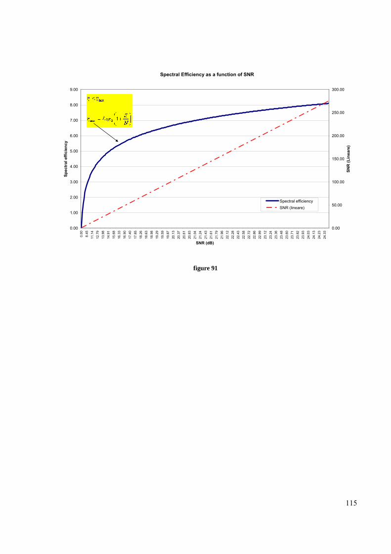
115
Spectral Efficiency as a function of SNR
0.00
1.00
2.00
3.00
4.00
5.00
6.00
7.00
8.00
9.00
0.00
8.45
11.1
412
.79
13.9
814
.91
15.6
816
.33
16.9
017
.40
17.8
518
.26
18.6
318
.98
19.2
919
.59
19.8
720
.13
20.3
720
.61
20.8
321
.04
21.2
421
.43
21.6
121
.79
21.9
622
.12
22.2
822
.43
22.5
822
.72
22.8
622
.99
23.1
223
.24
23.3
623
.48
23.6
023
.71
23.8
223
.93
24.0
324
.13
24.2
324
.33
SNR (dB)
Spec
tral
effi
cien
cy
0.00
50.00
100.00
150.00
200.00
250.00
300.00
SNR
(Lin
eare
)
Spectral efficiencySNR (lineare)
figure 91
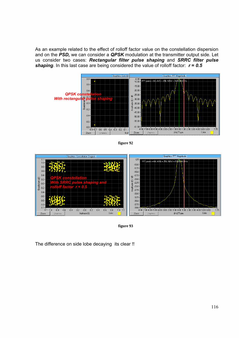
116
As an example related to the effect of rolloff factor value on the constellation dispersion and on the PSD, we can consider a QPSK modulation at the transmitter output side. Let us consider two cases: Rectangular filter pulse shaping and SRRC filter pulse shaping. In this last case are being considered the value of rolloff factor: r = 0.5
figure 92
figure 93
The difference on side lobe decaying its clear !!
QPSK constellation With rectangular pulse shaping
QPSK constellation With SRRC pulse shaping and rolloff factor r = 0.5
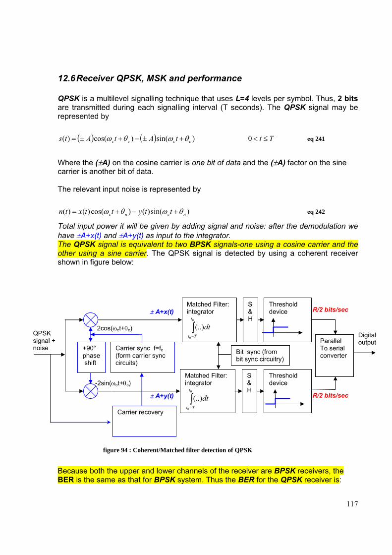
117
12.6 Receiver QPSK, MSK and performance QPSK is a multilevel signalling technique that uses L=4 levels per symbol. Thus, 2 bits are transmitted during each signalling interval (T seconds). The QPSK signal may be represented by
( ) ( ) TttAtAts cccc ≤<+±−+±= 0 )sin()cos()( θωθω eq 241
Where the (±A) on the cosine carrier is one bit of data and the (±A) factor on the sine carrier is another bit of data. The relevant input noise is represented by
)sin()()cos()()( ncnc ttyttxtn θωθω +−+= eq 242
Total input power it will be given by adding signal and noise: after the demodulation we have ±A+x(t) and ±A+y(t) as input to the integrator. The QPSK signal is equivalent to two BPSK signals-one using a cosine carrier and the other using a sine carrier. The QPSK signal is detected by using a coherent receiver shown in figure below:
figure 94 : Coherent/Matched filter detection of QPSK
Because both the upper and lower channels of the receiver are BPSK receivers, the BER is the same as that for BPSK system. Thus the BER for the QPSK receiver is:
± A+x(t)
Digital output
R/2 bits/sec
2cos(ωct+θc)
Carrier sync f=fc (form carrier sync circuits)
+90° phase shift
QPSK signal + noise Bit sync (from
bit sync circuitry)
R/2 bits/sec
Carrier recovery
Matched Filter: integrator
∫−
0
0
(..)t
Tt
dt
Threshold device
Threshold device
Matched Filter: integrator
∫−
0
0
(..)t
Tt
dt
Parallel To serial converter
-2sin(ωct+θc)
± A+y(t)
S&H
S&H
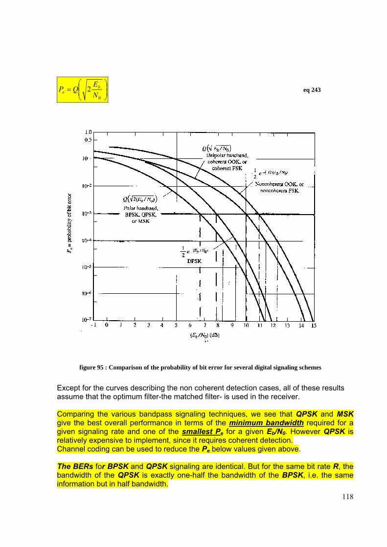
118
⎟⎟⎠
⎞⎜⎜⎝
⎛=
0
2NEQP b
e eq 243
figure 95 : Comparison of the probability of bit error for several digital signaling schemes
Except for the curves describing the non coherent detection cases, all of these results assume that the optimum filter-the matched filter- is used in the receiver. Comparing the various bandpass signaling techniques, we see that QPSK and MSK give the best overall performance in terms of the minimum bandwidth required for a given signaling rate and one of the smallest Pe for a given Eb/N0. However QPSK is relatively expensive to implement, since it requires coherent detection. Channel coding can be used to reduce the Pe below values given above. The BERs for BPSK and QPSK signaling are identical. But for the same bit rate R, the bandwidth of the QPSK is exactly one-half the bandwidth of the BPSK, i.e. the same information but in half bandwidth.
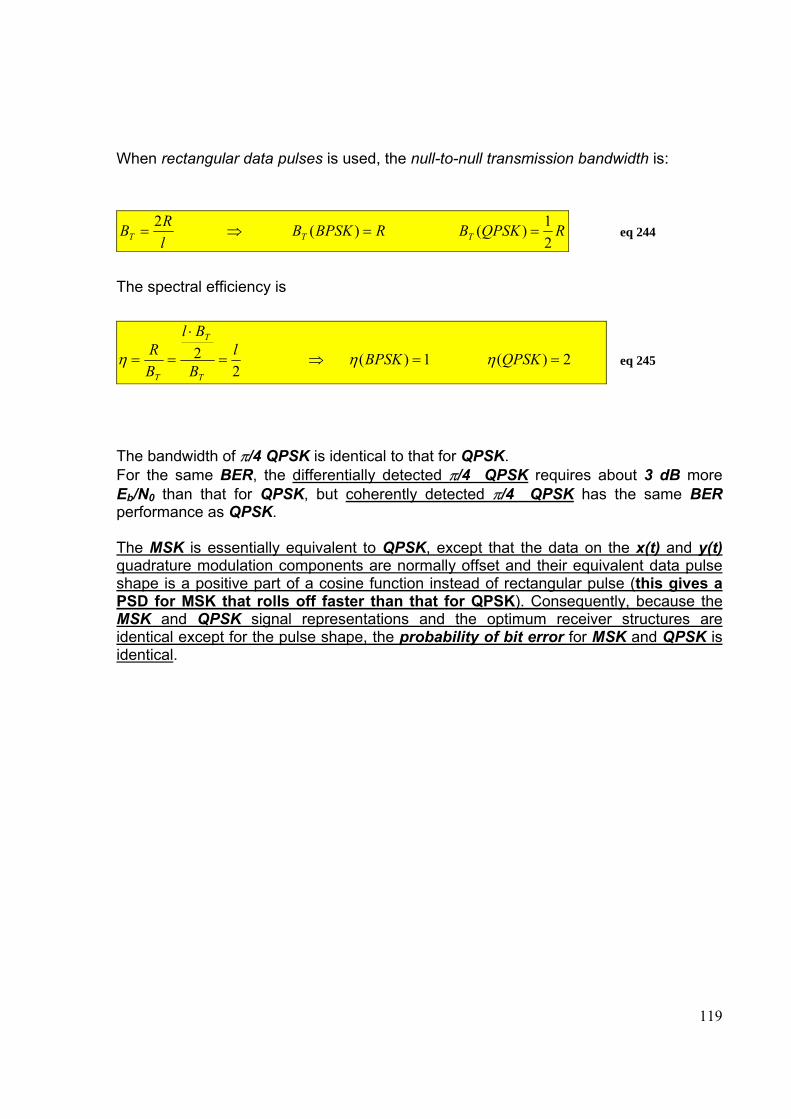
119
When rectangular data pulses is used, the null-to-null transmission bandwidth is:
RQPSKBRBPSKBlRB TTT 2
1)( )( 2==⇒= eq 244
The spectral efficiency is
2)( 1)( 2
2 QPSK BPSK lB
Bl
BR
T
T
T
==⇒=
⋅
== ηηη eq 245
The bandwidth of π/4 QPSK is identical to that for QPSK. For the same BER, the differentially detected π/4 QPSK requires about 3 dB more Eb/N0 than that for QPSK, but coherently detected π/4 QPSK has the same BER performance as QPSK. The MSK is essentially equivalent to QPSK, except that the data on the x(t) and y(t) quadrature modulation components are normally offset and their equivalent data pulse shape is a positive part of a cosine function instead of rectangular pulse (this gives a PSD for MSK that rolls off faster than that for QPSK). Consequently, because the MSK and QPSK signal representations and the optimum receiver structures are identical except for the pulse shape, the probability of bit error for MSK and QPSK is identical.
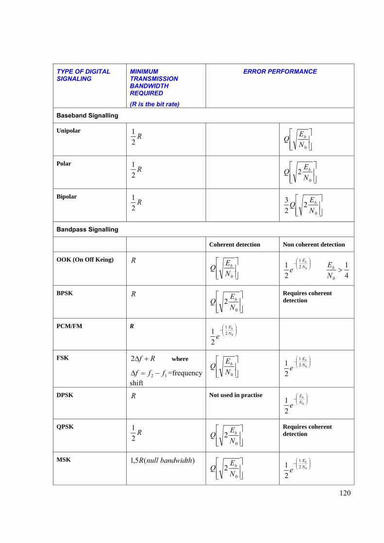
120
TYPE OF DIGITAL SIGNALING
MINIMUM TRANSMISSION BANDWIDTH REQUIRED
(R is the bit rate)
ERROR PERFORMANCE
Baseband Signalling
Unipolar R
21
⎥⎥⎦
⎤
⎢⎢⎣
⎡
0NEQ b
Polar R
21
⎥⎥⎦
⎤
⎢⎢⎣
⎡
0
2NEQ b
Bipolar R
21
⎥⎥⎦
⎤
⎢⎢⎣
⎡
0
223
NEQ b
Bandpass Signalling
Coherent detection Non coherent detection
OOK (On Off Keing) R
⎥⎥⎦
⎤
⎢⎢⎣
⎡
0NEQ b
41
21
0
21
0 >⎟⎟⎠
⎞⎜⎜⎝
⎛−
NEe bN
Eb
BPSK R
⎥⎥⎦
⎤
⎢⎢⎣
⎡
0
2NEQ b
Requires coherent detection
PCM/FM R ⎟⎟⎠
⎞⎜⎜⎝
⎛−
021
21 N
Eb
e
FSK Rf +∆2 where
12 fff −=∆ =frequency shift
⎥⎥⎦
⎤
⎢⎢⎣
⎡
0NEQ b ⎟⎟
⎠
⎞⎜⎜⎝
⎛−
021
21 N
Eb
e
DPSK R Not used in practise ⎟⎟⎠
⎞⎜⎜⎝
⎛−
0
21 N
Eb
e
QPSK R
21
⎥⎥⎦
⎤
⎢⎢⎣
⎡
0
2NEQ b
Requires coherent detection
MSK )(5,1 bandwidthnullR
⎥⎥⎦
⎤
⎢⎢⎣
⎡
0
2NEQ b ⎟⎟
⎠
⎞⎜⎜⎝
⎛−
021
21 N
Eb
e
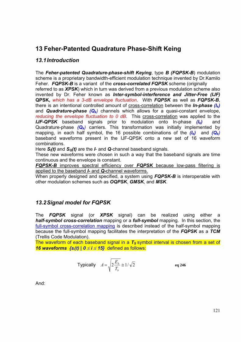
121
13 Feher-Patented Quadrature Phase-Shift Keing
13.1 Introduction The Feher-patented Quadrature-phase-shift Keying, type B (FQPSK-B) modulation scheme is a proprietary bandwidth-efficient modulation technique invented by Dr.Kamilo Feher. FQPSK-B is a variant of the cross-correlated FQPSK scheme (originally referred to as XPSK) which in turn was derived from a previous modulation scheme also invented by Dr. Feher known as Inter-symbol-interference and Jitter-Free (IJF) QPSK, which has a 3-dB envelope fluctuation. With FQPSK as well as FQPSK-B, there is an intentional controlled amount of cross-correlation between the In-phase (Ik) and Quadrature-phase (Qk) channels which allows for a quasi-constant envelope, reducing the envelope fluctuation to 0 dB. This cross-correlation was applied to the IJF-QPSK baseband signals prior to modulation onto In-phase (Ik) and Quadrature-phase (Qk) carriers. This transformation was initially implemented by mapping, in each half symbol, the 16 possible combinations of the (Ik) and (Qk) baseband waveforms present in the IJF-QPSK onto a new set of 16 waveform combinations. Here SI(t) and SQ(t) are the I- and Q-channel baseband signals. These new waveforms were chosen in such a way that the baseband signals are time continuous and the envelope is constant. FQPSK-B improves spectral efficiency over FQPSK because low-pass filtering is applied to the baseband I- and Q-channel waveforms. When properly designed and specified, a system using FQPSK-B is interoperable with other modulation schemes such as OQPSK, GMSK, and MSK.
13.2 Signal model for FQPSK The FQPSK signal (or XPSK signal) can be realized using either a half-symbol cross-correlation mapping or a full-symbol mapping. In this section, the full-symbol cross-correlation mapping is described instead of the half-symbol mapping because the full-symbol mapping facilitates the interpretation of the FQPSK as a TCM (Trellis Code Modulation). The waveform of each baseband signal in a TS symbol interval is chosen from a set of 16 waveforms {si(t) | 0 ≤ i ≤ 15} defined as follows:
Typically 2/12 ≅=b
b
TEA eq 246
And:
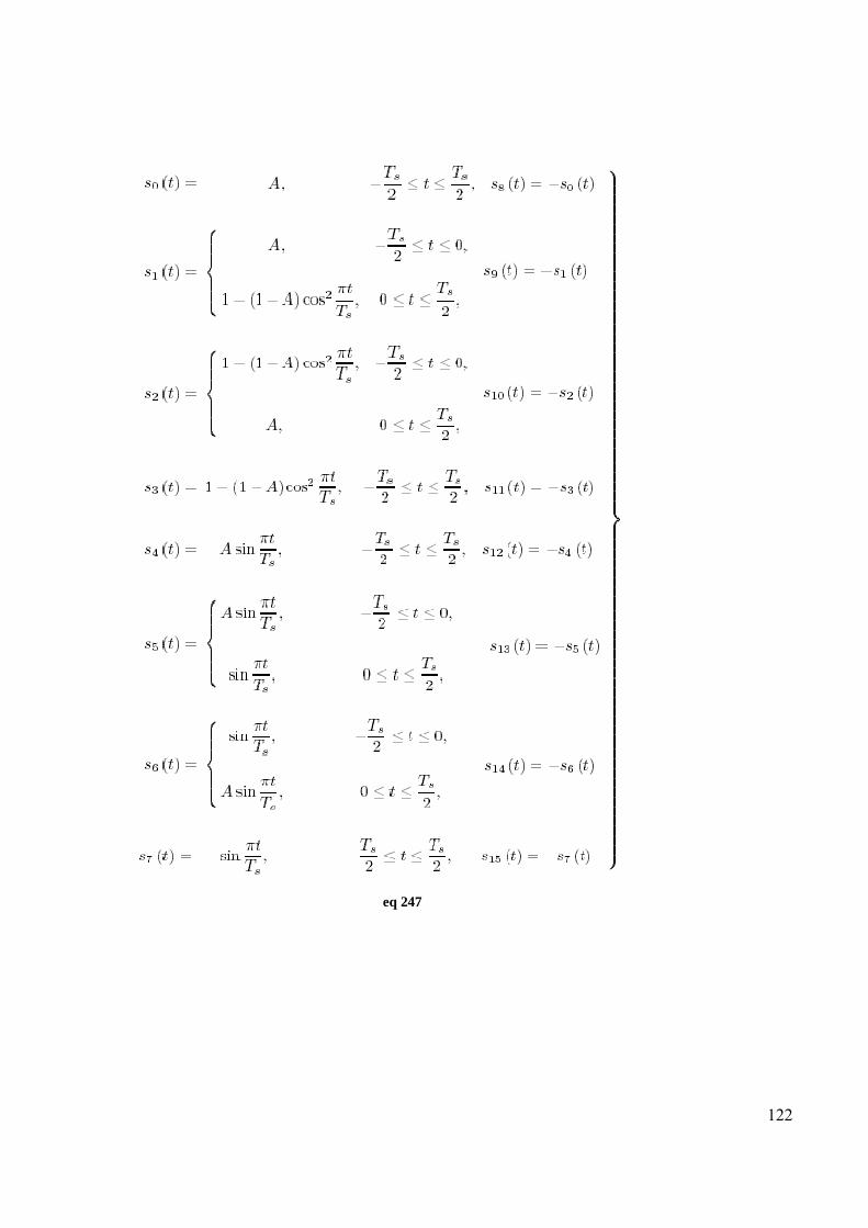
122
eq 247
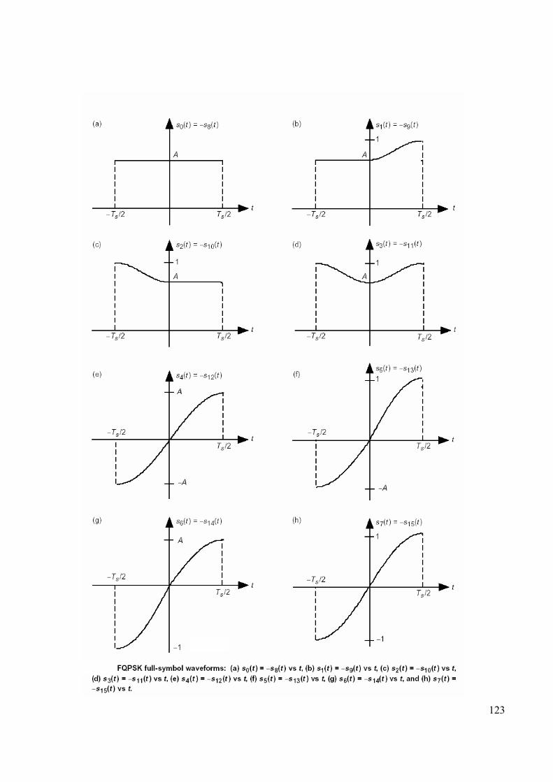
123
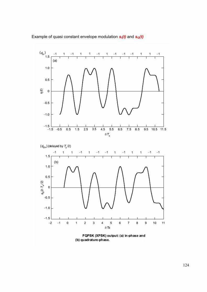
124
Example of quasi constant envelope modulation si(t) and sQ(t)
125
Note that for any value of A other then unity, s5(t) and s6(t) as well as their negatives, s13(t) and s14(t), will have a discontinuous slope at their midpoints (i.e., at t = 0), whereas the remaining 12 waveforms all have a continuous slope throughout their defining intervals. Also note that all 16 waveforms have zero slope at their end points and, thus, concatenation of any pair of these will not result in a slope discontinuity. The wavelets are numbered according to a Trellis mapping rule that determines which wavelet is transmitted. Specifically, the mapping rule specifies that during the n-th channel symbol interval, [(n - [1/2])Ts] ≤ t ≤ [(n + [1/2])Ts], the baseband I- and Q-channel waveforms Ik and QK are assigned wavelets sI(t)=si and sQ(t)=sj respectively, where the indices i and j are given by:
00
11
22
33
00
11
22
33
2222
2222
×+×+×+×=
×+×+×+×=
QQQQj
IIIIi eq 248
with
nI
nInI
nQnQ
nQnQ
dIddI
ddI
ddI
,3
1,,2
2,1,1
1,,0
=
⊕=
⊕=
⊕=
−
−−
−
nQ
nQnQ
nInI
nInI
dQ
IddQIddQ
ddQ
,3
01,,2
21,,1
1,1,0
=
=⊕=
=⊕=
⊕=
−
−
+
eq 249
Where { }1,0 and ,, ∈nQnI dd are the n-th I- and Q- channel inputs to the modulator respectively The particular sI(t) and sQ(t) waveforms chosen for any particular Ts signalling interval on each channel depend on the most recent data transition on that channel, as well as the two most recent successive transition on the other channel. Next, define the following mapping function for the baseband I-channel transmitted waveform [yI (t)=sI (t) ] in the n-th signalling interval [(n - [1/2])Ts] ≤ t ≤[(n + [1/2])Ts] in terms of the transition properties of the I and Q data symbol sequences dIn and dQn, respectively.
126
Making use of the signal properties of eq above, the mapping conditions in (1) through (4) for the I-channel baseband output can be summarized in a concise form described by Table 1. A similar construction for the baseband Q-channel transmitted waveform [yQ(t)=sQ(t-Ts/2) ] in the n-th signalling interval nTs ≤ t ≤ (n + 1)Ts in terms of the transition properties of the I and Q data symbol sequences, dIn and dQn, respectively,
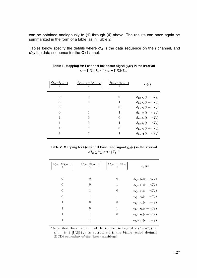
127
can be obtained analogously to (1) through (4) above. The results can once again be summarized in the form of a table, as in Table 2. Tables below specify the details where dIK is the data sequence on the I channel, and dQK the data sequence for the Q channel.
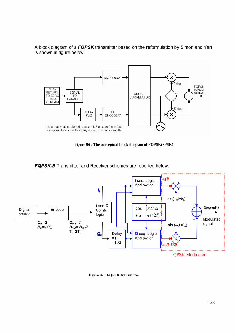
128
A block diagram of a FQPSK transmitter based on the reformulation by Simon and Yan is shown in figure below:
figure 96 : The conceptual block diagram of FQPSK(SPSK)
FQPSK-B Transmitter and Receiver schemes are reported below:
figure 97 : FQPSK transmitter
Modulated signal
Ik
cos(ωct+θc)
[ ]sTt 2/cos π= [ ]sTt 2/sin π=
SFQPSK(t) Digital source
sin (ωct+θc) Qin=2 Bin=1/Tb
Encoder
Qout=4 Bout= Bin /2 Ts=2Tb
I and Q Comb logic
Delay=Tb =Ts/2
Qk Q seq. Logic And switch
I seq. Logic And switch
si(t)
sQ(t-T/2)
+
+
QPSK Modulator
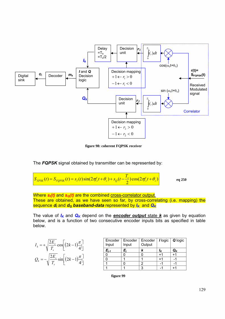
129
figure 98: coherent FQPSK receiver
The FQPSK signal obtained by transmitter can be represented by:
)2cos()2
()2sin()()()( ccs
QccIFQPSKXPSK tfTtstftstStS θπθπ +−++== eq 250
Where sI(t) and sQ(t) are the combined cross-correlator output. These are obtained, as we have seen so far, by cross-correlating (i.e. mapping) the sequence dI and dQ baseband-data represented by IK and QK The value of IK and QK depend on the encoder output state k as given by equation below, and is a function of two consecutive encoder inputs bits as specified in table below.
( )
( ) ⎥⎦⎤
⎢⎣⎡ −−=
⎥⎦⎤
⎢⎣⎡ −+=
412sin2
412cos2
π
π
kTEQ
kTEI
s
sk
s
sk
figure 99
EncoderInput
Encoder Input
Encoder Output
I logic Q logic
Ej-1 Ej k IK QK 0 0 0 +1 +1 0 1 1 +1 -1 1 0 2 -1 -1 1 1 3 -1 +1
Ik
Received Modulated signal
cos(ωct+θc) r(t)= SFQPSK(t) Digital
sink
sin (ωct+θc)
ei Decoder mk I and Q Decision logic
Delay=Tb =Ts/2
Qk
∫bT
dt0
(.)
∫bT
dt0
(.)
Decision unit
Decision unit
r2
Decision mapping
0101
1
1
<←−>←+
rr
Decision mapping
0101
2
2
<←−>←+
rr
Correlator
r1
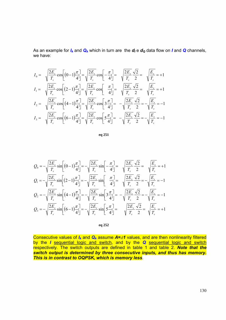
130
As an example for Ik and Qk which in turn are the dI e dQ data flow on I and Q channels, we have:
( )
( )
( )
( ) 1222
45cos2
416cos2
1222
43cos2
414cos2
1222
4cos2
412cos2
1222
4cos2
410cos2
3
2
1
0
−=−=−=⎥⎦⎤
⎢⎣⎡=⎥⎦
⎤⎢⎣⎡ −=
−=−=−=⎥⎦⎤
⎢⎣⎡=⎥⎦
⎤⎢⎣⎡ −=
+===⎥⎦⎤
⎢⎣⎡=⎥⎦
⎤⎢⎣⎡ −=
+===⎥⎦⎤
⎢⎣⎡−=⎥⎦
⎤⎢⎣⎡ −=
s
s
s
s
s
s
s
s
s
s
s
s
s
s
s
s
s
s
s
s
s
s
s
s
s
s
s
s
s
s
s
s
TE
TE
TE
TEI
TE
TE
TE
TEI
TE
TE
TE
TEI
TE
TE
TE
TEI
ππ
ππ
ππ
ππ
eq 251
( )
( )
( )
( ) 1222
45sin2
416sin2
1222
43sin2
414sin2
1222
4sin2
412sin2
1222
4sin2
410sin2
3
2
1
0
+===⎥⎦⎤
⎢⎣⎡−=⎥⎦
⎤⎢⎣⎡ −−=
−=−=−=⎥⎦⎤
⎢⎣⎡−=⎥⎦
⎤⎢⎣⎡ −−=
−=−==⎥⎦⎤
⎢⎣⎡−=⎥⎦
⎤⎢⎣⎡ −−=
+===⎥⎦⎤
⎢⎣⎡−−=⎥⎦
⎤⎢⎣⎡ −−=
s
s
s
s
s
s
s
s
s
s
s
s
s
s
s
s
s
s
s
s
s
s
s
s
s
s
s
s
s
s
s
s
TE
TE
TE
TEQ
TE
TE
TE
TEQ
TE
TE
TE
TEQ
TE
TE
TE
TEQ
ππ
ππ
ππ
ππ
eq 252
Consecutive values of Ik and Qk assume A=±1 values, and are then nonlinearity filtered by the I sequential logic and switch, and by the Q sequential logic and switch respectively. The switch outputs are defined in table 1 and table 2. Note that the switch output is determined by three consecutive inputs, and thus has memory. This is in contrast to OQPSK, which is memory less.

131
13.3 Signal model for FQPSK-B The FQPSK-B signal obtained by transmitter can be represented by:
)2cos()2
(~)2sin()(~)()( ccs
QccIBFQPSKXPSK tfTtstftstStS θπθπ +−++== − eq 253
where the filtered signals
∫
∫
∞−
∞−
−=
−=
t
t
II
dthtsts
dthtsts
ττ
ττ
)()()(~
)()()(~
eq 254
are the low pass filtered version of the sI(t) and sQ(t) seen so far in FQPSK form, and h(t) is the impulse response of the low-pass filter. The functional block diagram below depicts full-symbol cross-correlation mapping followed by the transmission filter and an Offset-QPSK (OQPSK) modulator.
figure 100 : FQPSK-B modulator
Figure below shows the phasor diagrams and the eye diagrams of both FQPSK and FQPSK-B baseband signals.
sI(t)
SQ(t)
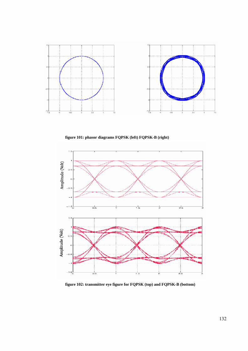
132
figure 101: phasor diagrams FQPSK (left) FQPSK-B (right)
figure 102: transmitter eye figure for FQPSK (top) and FQPSK-B (bottom)
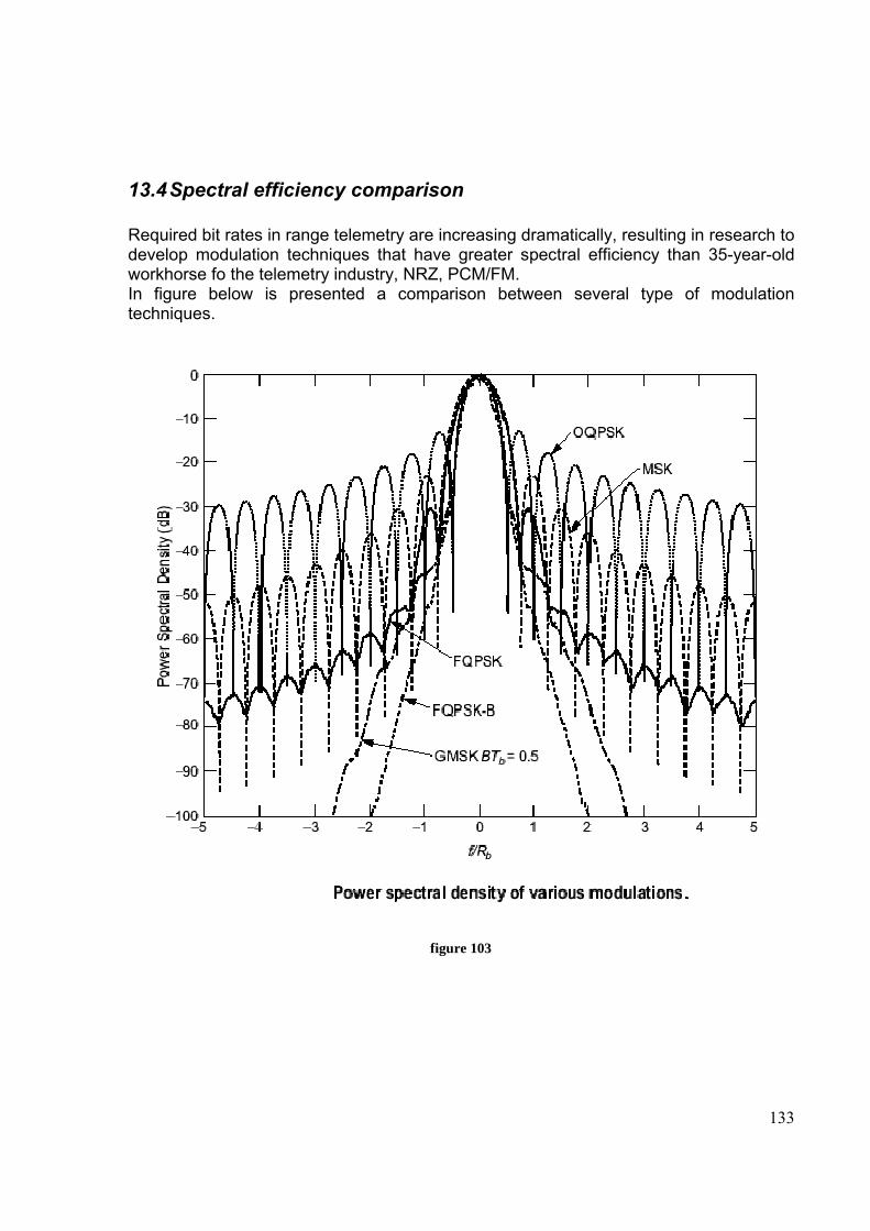
133
13.4 Spectral efficiency comparison Required bit rates in range telemetry are increasing dramatically, resulting in research to develop modulation techniques that have greater spectral efficiency than 35-year-old workhorse fo the telemetry industry, NRZ, PCM/FM. In figure below is presented a comparison between several type of modulation techniques.
figure 103
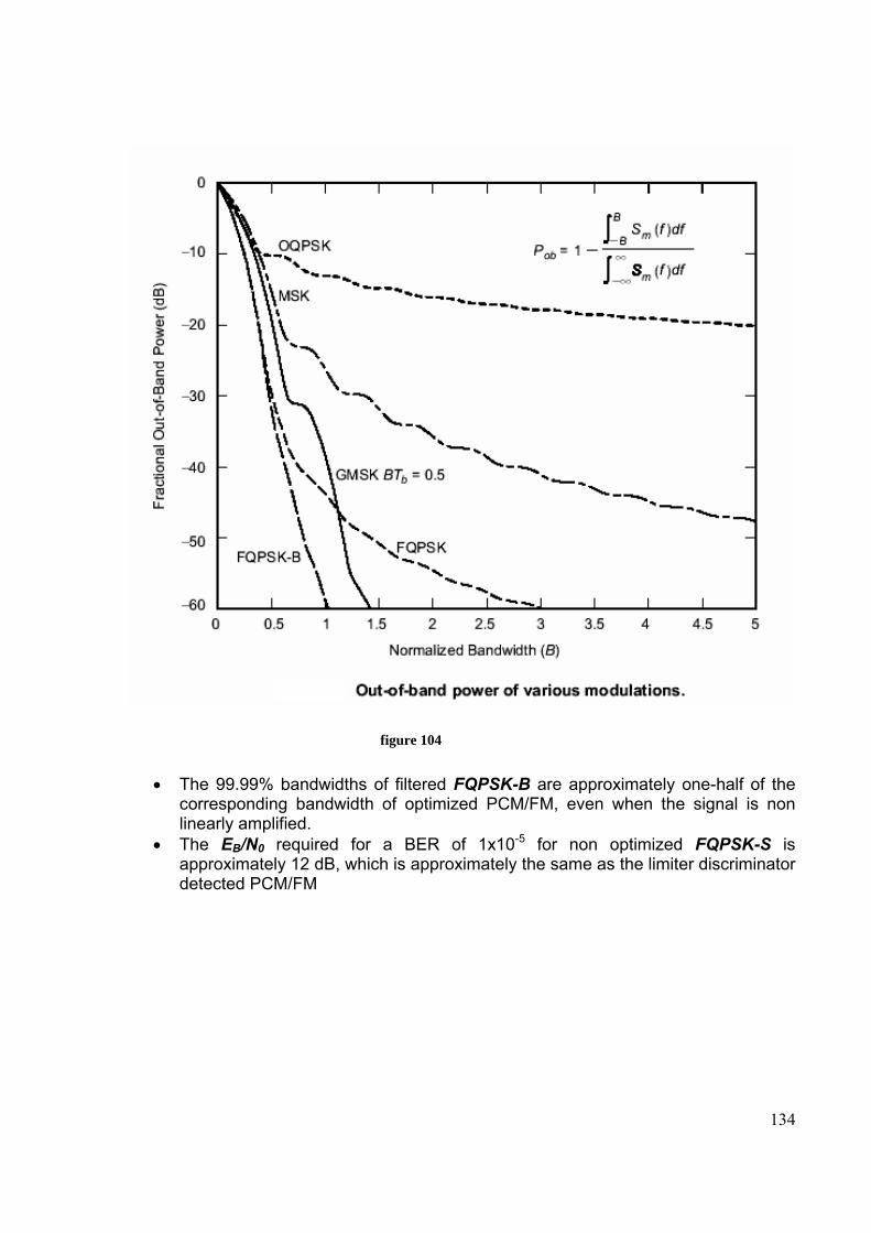
134
figure 104
• The 99.99% bandwidths of filtered FQPSK-B are approximately one-half of the
corresponding bandwidth of optimized PCM/FM, even when the signal is non linearly amplified.
• The EB/N0 required for a BER of 1x10⁻⁵ for non optimized FQPSK-S is approximately 12 dB, which is approximately the same as the limiter discriminator detected PCM/FM
135
14 EFFICIENT MODULATION METHODS STUDY AT NASA/JPL CCSDS (RF and Modulation) became aware of a new modulation type at its Spring 1997 meeting. Named FQPSK for its inventor, Dr. Kamilo Feher, it was reported to have a very narrow RF spectrum and only minimal end-to-end system losses. Test data provided by Dr. Feher showed a spectrum narrower than that of GMSK using a BTS = 0.50 filter. Sideband attenuations were tabulated for the several modulation types studied and it was concluded that FQPSK-B could be a very attractive modulation method. FQPSK-B, a specific version of FQPSK, was simulated using SPW. Additionally, Mr. Eugene Law of the Naval Air Warfare Center Weapons Division at Point Mugu obtained an FQPSK-B modulator-demodulator (modem) for hardware tests. NASA witnessed these spectrum tests and obtained copies of the spectra. Note: This is the only modulation type covered in this report for which there are actual hardware verification tests. These tests confirm the simulation results reported here.
• FQPSK-B modulation is a form of OQPSK modulation in which one of 16 wavelets [waveforms] is selected for transmission on the I-channel and another is chosen for transmission on the Q-channel. Wavelet determination depends on the present and previous data bit pair values for the I and Q channels. There is a ½-symbol-time offset between I and Q transmissions.
• FQPSK-B modulates and filters at baseband. There after, the signal is translated to an i.f. frequency and then translated again to the transmitted RF frequency.
14.1 FQPSK-B Modulation Bit-Error-Rate (BER) Simulations of FQPSK-B were conducted at JPL with the assistance of Dr. Feher. Figure below shows the Bit-Error-Rate (BER) performance. Like MSK and GMSK modulation, existing transmitting and receiving equipment simulation models were unsuitable for FQPSK-B. However, BER performance was measured using ESA’s power amplifier operating in full saturation. Comparing FQPSK-B to ideal BPSK/NRZ shows that an additional EB / N0 of 1.7 dB is required to achieve a 1 x 10⁻³
BER. This is 0.3 dB greater than GMSK with a BTS = 0.5. Dr. Feher commented that additional system optimization might reduce these losses. His suggestions included adding hard limiters to the transmitting system and improving the receiver filter’s phase performance. Supporting his position, Dr. Feher points to BER measurements made at Point Mugu using actual hardware. Dr. Feher’s modem, operating with a 1 Watt SSPA in full saturation, produced a 1 x 10⁻³ BER at an EB / N0 of 8 dB, about 1.3 dB more than ideal BPSK/NRZ and 0.1 dB less than GMSK with a BTS = 0.5. Further BER tests will be required to verify the better EB / N0 performance using a modulator capable of a 60 dB sideband attenuation.
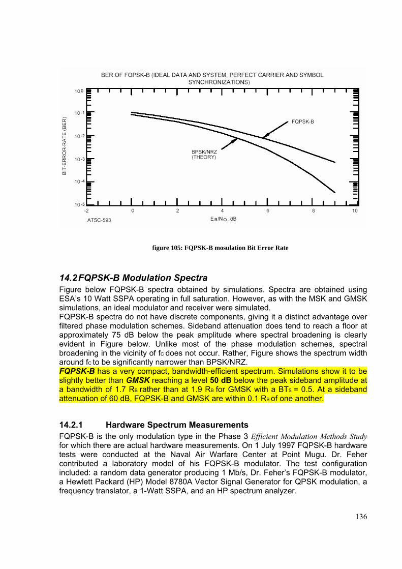
136
figure 105: FQPSK-B mosulation Bit Error Rate
14.2 FQPSK-B Modulation Spectra Figure below FQPSK-B spectra obtained by simulations. Spectra are obtained using ESA’s 10 Watt SSPA operating in full saturation. However, as with the MSK and GMSK simulations, an ideal modulator and receiver were simulated. FQPSK-B spectra do not have discrete components, giving it a distinct advantage over filtered phase modulation schemes. Sideband attenuation does tend to reach a floor at approximately 75 dB below the peak amplitude where spectral broadening is clearly evident in Figure below. Unlike most of the phase modulation schemes, spectral broadening in the vicinity of fC does not occur. Rather, Figure shows the spectrum width around fC to be significantly narrower than BPSK/NRZ. FQPSK-B has a very compact, bandwidth-efficient spectrum. Simulations show it to be slightly better than GMSK reaching a level 50 dB below the peak sideband amplitude at a bandwidth of 1.7 RB rather than at 1.9 RB for GMSK with a BTS = 0.5. At a sideband attenuation of 60 dB, FQPSK-B and GMSK are within 0.1 RB of one another.
14.2.1 Hardware Spectrum Measurements FQPSK-B is the only modulation type in the Phase 3 Efficient Modulation Methods Study for which there are actual hardware measurements. On 1 July 1997 FQPSK-B hardware tests were conducted at the Naval Air Warfare Center at Point Mugu. Dr. Feher contributed a laboratory model of his FQPSK-B modulator. The test configuration included: a random data generator producing 1 Mb/s, Dr. Feher’s FQPSK-B modulator, a Hewlett Packard (HP) Model 8780A Vector Signal Generator for QPSK modulation, a frequency translator, a 1-Watt SSPA, and an HP spectrum analyzer.
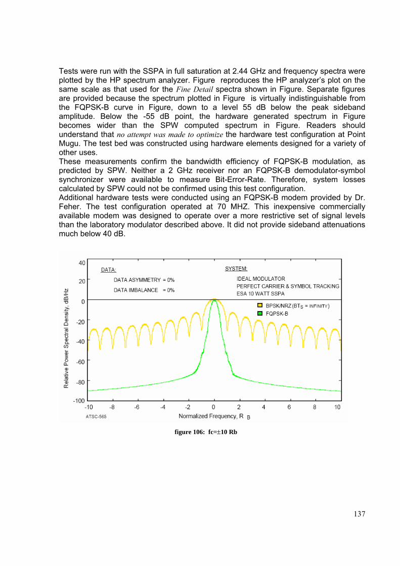
137
Tests were run with the SSPA in full saturation at 2.44 GHz and frequency spectra were plotted by the HP spectrum analyzer. Figure reproduces the HP analyzer’s plot on the same scale as that used for the Fine Detail spectra shown in Figure. Separate figures are provided because the spectrum plotted in Figure is virtually indistinguishable from the FQPSK-B curve in Figure, down to a level 55 dB below the peak sideband amplitude. Below the -55 dB point, the hardware generated spectrum in Figure becomes wider than the SPW computed spectrum in Figure. Readers should understand that no attempt was made to optimize the hardware test configuration at Point Mugu. The test bed was constructed using hardware elements designed for a variety of other uses. These measurements confirm the bandwidth efficiency of FQPSK-B modulation, as predicted by SPW. Neither a 2 GHz receiver nor an FQPSK-B demodulator-symbol synchronizer were available to measure Bit-Error-Rate. Therefore, system losses calculated by SPW could not be confirmed using this test configuration. Additional hardware tests were conducted using an FQPSK-B modem provided by Dr. Feher. The test configuration operated at 70 MHZ. This inexpensive commercially available modem was designed to operate over a more restrictive set of signal levels than the laboratory modulator described above. It did not provide sideband attenuations much below 40 dB.
figure 106: fc=±10 Rb
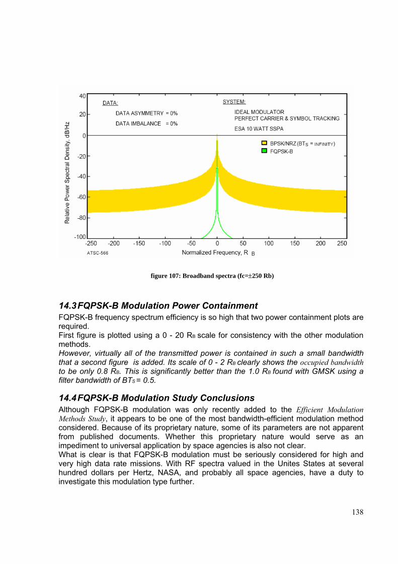
138
figure 107: Broadband spectra (fc=±250 Rb)
14.3 FQPSK-B Modulation Power Containment FQPSK-B frequency spectrum efficiency is so high that two power containment plots are required. First figure is plotted using a 0 - 20 RB scale for consistency with the other modulation methods. However, virtually all of the transmitted power is contained in such a small bandwidth that a second figure is added. Its scale of 0 - 2 RB clearly shows the occupied bandwidth to be only 0.8 RB. This is significantly better than the 1.0 RB found with GMSK using a filter bandwidth of BTS = 0.5.
14.4 FQPSK-B Modulation Study Conclusions Although FQPSK-B modulation was only recently added to the Efficient Modulation Methods Study, it appears to be one of the most bandwidth-efficient modulation method considered. Because of its proprietary nature, some of its parameters are not apparent from published documents. Whether this proprietary nature would serve as an impediment to universal application by space agencies is also not clear. What is clear is that FQPSK-B modulation must be seriously considered for high and very high data rate missions. With RF spectra valued in the Unites States at several hundred dollars per Hertz, NASA, and probably all space agencies, have a duty to investigate this modulation type further.
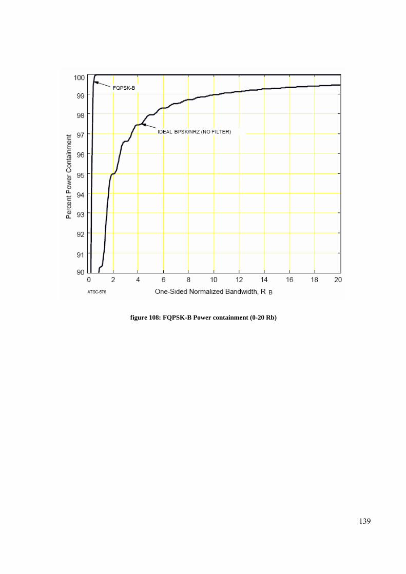
139
figure 108: FQPSK-B Power containment (0-20 Rb)
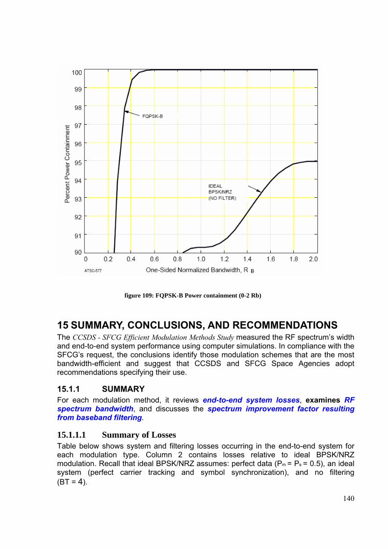
140
figure 109: FQPSK-B Power containment (0-2 Rb)
15 SUMMARY, CONCLUSIONS, AND RECOMMENDATIONS The CCSDS - SFCG Efficient Modulation Methods Study measured the RF spectrum’s width and end-to-end system performance using computer simulations. In compliance with the SFCG’s request, the conclusions identify those modulation schemes that are the most bandwidth-efficient and suggest that CCSDS and SFCG Space Agencies adopt recommendations specifying their use.
15.1.1 SUMMARY For each modulation method, it reviews end-to-end system losses, examines RF spectrum bandwidth, and discusses the spectrum improvement factor resulting from baseband filtering.
15.1.1.1 Summary of Losses Table below shows system and filtering losses occurring in the end-to-end system for each modulation type. Column 2 contains losses relative to ideal BPSK/NRZ modulation. Recall that ideal BPSK/NRZ assumes: perfect data (Pm = Ps = 0.5), an ideal system (perfect carrier tracking and symbol synchronization), and no filtering (BT = 4).
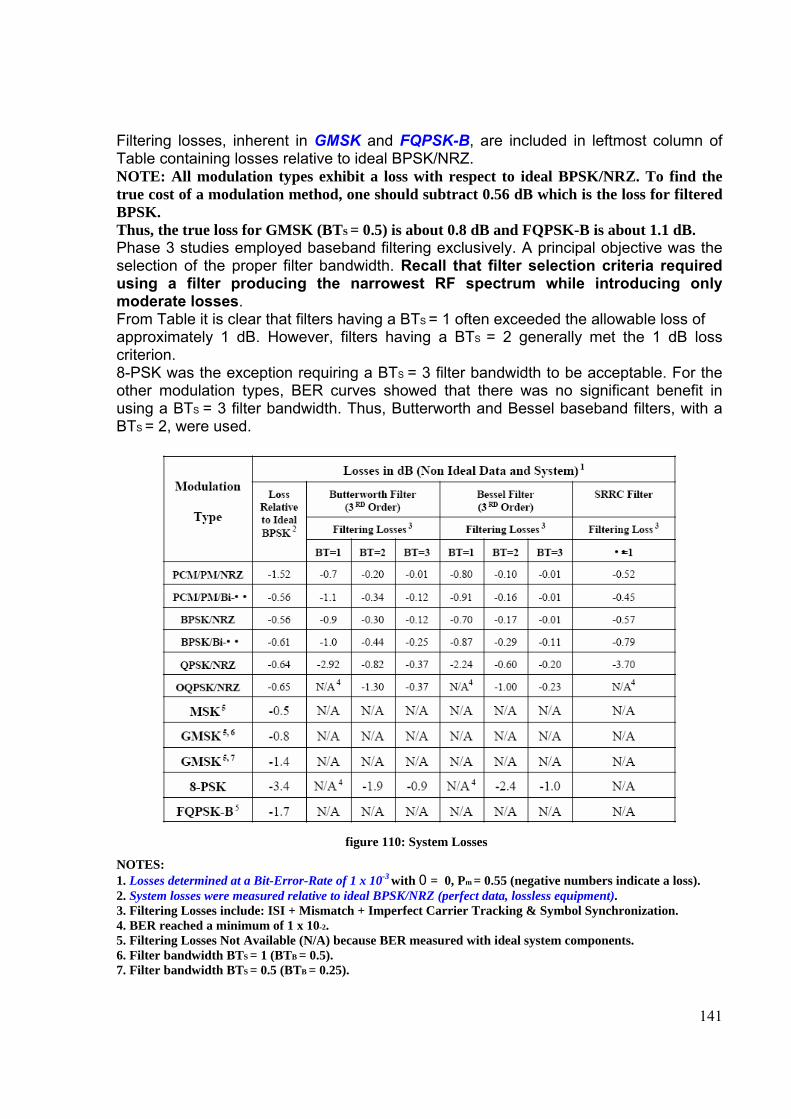
141
Filtering losses, inherent in GMSK and FQPSK-B, are included in leftmost column of Table containing losses relative to ideal BPSK/NRZ. NOTE: All modulation types exhibit a loss with respect to ideal BPSK/NRZ. To find the true cost of a modulation method, one should subtract 0.56 dB which is the loss for filtered BPSK. Thus, the true loss for GMSK (BTS = 0.5) is about 0.8 dB and FQPSK-B is about 1.1 dB. Phase 3 studies employed baseband filtering exclusively. A principal objective was the selection of the proper filter bandwidth. Recall that filter selection criteria required using a filter producing the narrowest RF spectrum while introducing only moderate losses. From Table it is clear that filters having a BTS = 1 often exceeded the allowable loss of approximately 1 dB. However, filters having a BTS = 2 generally met the 1 dB loss criterion. 8-PSK was the exception requiring a BTS = 3 filter bandwidth to be acceptable. For the other modulation types, BER curves showed that there was no significant benefit in using a BTS = 3 filter bandwidth. Thus, Butterworth and Bessel baseband filters, with a BTS = 2, were used.
figure 110: System Losses
NOTES: 1. Losses determined at a Bit-Error-Rate of 1 x 10⁻³
with 0 = 0, Pm = 0.55 (negative numbers indicate a loss). 2. System losses were measured relative to ideal BPSK/NRZ (perfect data, lossless equipment). 3. Filtering Losses include: ISI + Mismatch + Imperfect Carrier Tracking & Symbol Synchronization. 4. BER reached a minimum of 1 x 10⁻². 5. Filtering Losses Not Available (N/A) because BER measured with ideal system components. 6. Filter bandwidth BTS = 1 (BTB = 0.5). 7. Filter bandwidth BTS = 0.5 (BTB = 0.25).
142
15.1.1.2 RF Spectrum Efficiency Another Phase 3 study objective was to determine the RF spectral bandwidth of each modulation type. This was necessary to rank the several modulation methods with respect to one-another. Many Spectrum Managers are concerned principally with occupied bandwidth (i.e., 99% power containment). The Efficient Modulation Methods Study was motivated by a desire to pack a substantially greater number of spacecraft into a given frequency allocation, particularly in the 2 and 8 GHz Category A mission bands. Maximum packing density occurs when spectra from two spacecraft, operating on adjacent frequencies, just begin to overlap at n dB below the peak of the data sideband’s spectrum. This follows from a worst-case assumption that the Earth station’s antenna is bore sighted on both spacecraft simultaneously. Where spacecraft are not coincidently within the Earth station antenna’s beamwidth, the interferer’s and victim’s relative signal strengths will determine the special separation necessary to avoid interference. Obviously, even as frequency band usage increases, some spatial separation is expected. This study attempted to determine the value of n. Views differ regarding the optimal value of n. Some believe that spectra from spacecraft on adjacent frequencies could be permitted to intersect at a level of 20 dB below the peak sideband amplitude. Others believe that the number should be greater or less than 20 dB. In any event, Category A missions in highly elliptical orbits can undergo signal level changes of 30 dB or more at the Earth’s surface. Thus, it would seem prudent to prohibit RF spectra, from spacecraft operating on adjacent frequencies, from intersecting at levels higher than 50 dB below the peak of the data sideband generated by the spacecraft having the stronger signal. To provide maximum flexibility, RF spectrum bandwidths have been tabulated at values of n from 20 to 60 (dB) below the data sideband’s peak. RF spectrum width increases as a function of n and each user must select the proper value. A value of n = 50 is recommended for most applications. For a specific value of n, one can calculate the improvement in spectral efficiency. CCSDS concluded that BPSK/NRZ was to be the reference modulation type. A Spectrum Improvement Factor (SIF) can be calculated by comparing the bandwidth of unfiltered BPSK/NRZ to the bandwidth of the modulation method under discussion according to the relationship:
eq 255
Since the bandwidth is a function of n, the SIF will also vary with n. Table below contains the bandwidths and SIFs at several values of n for all modulation types covered in this Phase 3 study.
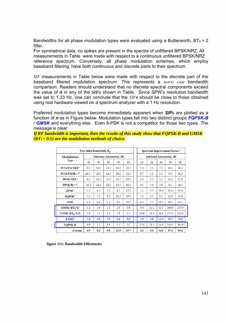
143
Bandwidths for all phase modulation types were evaluated using a Butterworth, BTS = 2 filter. For symmetrical data, no spikes are present in the spectra of unfiltered BPSK/NRZ. All measurements in Table were made with respect to a continuous unfiltered BPSK/NRZ reference spectrum. Conversely, all phase modulation schemes, which employ baseband filtering, have both continuous and discrete parts to their spectrum. SIF measurements in Table below were made with respect to the discrete part of the baseband filtered modulation spectrum. This represents a worst case bandwidth comparison. Readers should understand that no discrete spectral components exceed the value of n in any of the SIFs shown in Table. Since SPW’s resolution bandwidth was set to 1.33 Hz, one can conclude that the SIFs should be close to those obtained using real hardware viewed on a spectrum analyzer with a 1 Hz resolution. Preferred modulation types become immediately apparent when SIFs are plotted as a function of n as in Figure below. Modulation types fall into two distinct groups FQPSK-B / GMSK and everything else. Even 8-PSK is not a competitor for those two types. The message is clear: If RF bandwidth is important, then the results of this study show that FQPSK-B and GMSK (BTS = 0.5) are the modulation methods of choice.
figure 111: Bandwidth Efficiencies
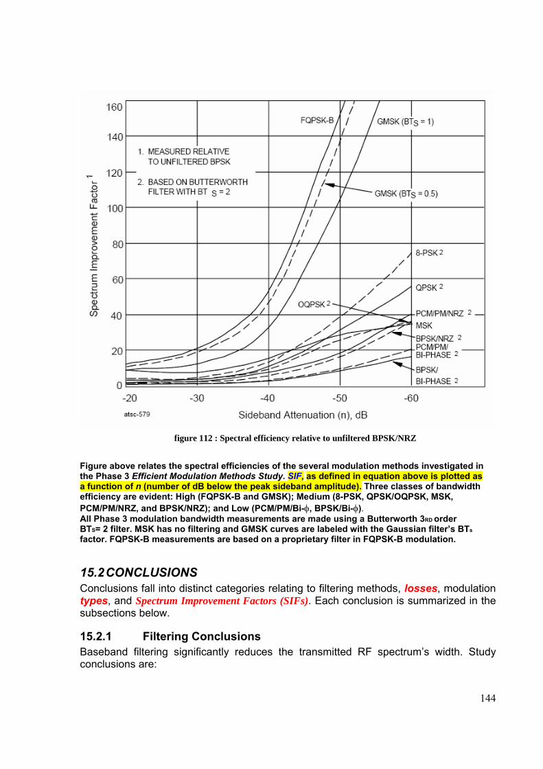
144
figure 112 : Spectral efficiency relative to unfiltered BPSK/NRZ
Figure above relates the spectral efficiencies of the several modulation methods investigated in the Phase 3 Efficient Modulation Methods Study. SIF, as defined in equation above is plotted as a function of n (number of dB below the peak sideband amplitude). Three classes of bandwidth efficiency are evident: High (FQPSK-B and GMSK); Medium (8-PSK, QPSK/OQPSK, MSK, PCM/PM/NRZ, and BPSK/NRZ); and Low (PCM/PM/Bi-φ, BPSK/Bi-φ). All Phase 3 modulation bandwidth measurements are made using a Butterworth 3RD order BTS= 2 filter. MSK has no filtering and GMSK curves are labeled with the Gaussian filter’s BTs
factor. FQPSK-B measurements are based on a proprietary filter in FQPSK-B modulation.
15.2 CONCLUSIONS Conclusions fall into distinct categories relating to filtering methods, losses, modulation types, and Spectrum Improvement Factors (SIFs). Each conclusion is summarized in the subsections below.
15.2.1 Filtering Conclusions Baseband filtering significantly reduces the transmitted RF spectrum’s width. Study conclusions are:
145
• Filtering of transmitted signals will be required to obtain an acceptably narrow RF spectrum.
• Hardware limitations make post PA filtering impractical at data rates below about 8 Ms/s.
o Realizable Qs limit the filter’s bandwidth to about 1-2% of the transmitted frequency.
o Filtering power losses may be unacceptable, even at a 1-2% bandwidth. o For low data symbol rates, post PA filtering may make turnaround
ranging difficult. • Depending upon its architecture, transponder i.f. filtering may not be practical.
o Q limitations stated above apply if modulation occurs at the transmitting frequency.
o Filtering at i.f. requires transponders be modified for each mission. o Filtering at i.f. makes data rate changes difficult. o For low data symbol rates, i.f. filtering may make turnaround ranging
difficult. o Filtering within the transponder risks introducing spurious emissions
causing lock-up. • Baseband filtering is the only practical alternative to unacceptable post PA and
i.f. filtering. o Baseband filtering can be accomplished with a simple, passive low-pass
filter design. A 3RD order Butterworth filter (BTS = 2) provides the best
performance-simplicity ratio. o Filtering prior to phase modulation produces undesirable spikes in the RF
spectrum. Spikes can only be avoided by using a different modulation method
(GMSK, FQPSK). • Both GMSK and FQPSK-B utilize baseband filtering and do not require i.f. nor
post PA filters.
15.2.2 Loss Conclusions Table above partitions losses into two categories: System (losses relative to ideal BPSK) and Filtering (ISI and Mismatch). One criterion for the Phase 3 study was that end-to-end losses should be reasonable. CCSDS determined that approximately 1 dB was reasonable. The following conclusions regarding losses were reached:
• High system loss (1.5 dB) found for PCM/PM/NRZ, resulted from a 10% data imbalance.
o When a BTS = 2 Butterworth filter is used, data imbalance should not exceed 5%.
• 8-PSK modulation exhibits an excessive system loss (3.4 dB). o Filtering losses decreased for non-constant envelope modulation.
However, spectrum width increased. Losses were not reduced to an acceptable level.
o High losses make 8-PSK modulation unsuitable for power-limited Category A missions.
• GMSK (BTS =0.5) also exhibited high (1.4 dB) system losses.
146
o Increasing filter bandwidth to BTS = 1 reduced system losses to an acceptable level.
o Losses were measured with an ideal (lossless) receiver. • FQPSK-B losses were found to be a high 1.7 dB.
o Losses were also measured with an ideal (lossless) receiver.
15.2.3 Modulation Methods Conclusions Figures above , graphically identify the preferred modulation methods. For the several modulation methods considered, the following conclusions were reached.
• FQPSK-B provides the narrowest RF spectrum of all modulation methods studied.
o FQPSK-B should be considered for all high and very high data rate missions.
Provided that losses are acceptable. • GMSK, with a filter bandwidth BTS = 0.5, produces virtually equivalent results to
FQPSK-B. o Further work is required to validate system losses using real hardware.
• 8-PSK, with its high losses, does not appear useful for most Category A missions.
o Excessive losses and modest performance gains do not provide sufficient advantages.
• QPSK has comparatively poorer bandwidth efficiency than does FQPSK-B and GMSK.
o Its common usage may dictate its consideration in some applications. o Absent spread spectrum, QPSK cannot provide simultaneous telemetry
and ranging. • OQPSK could not be evaluated properly with the UPM.
o OQPSK should be reserved for applications requiring separate, independent data channels.
o Orthogonally phased BPSK/NRZ modulators, with a ½ symbol offset should be used.
• BPSK/NRZ has poor bandwidth efficiency and should not be used if bandwidth is important.
o Bandwidth efficiency is slightly lower than PCM/PM/NRZ modulation. o BPSK/NRZ may be an alternative to PCM/PM/NRZ when:
A residual carrier is not required. The data imbalance is so great that PCM/PM/NRZ would suffer
excessive losses. • PCM/PM/NRZ has poor bandwidth efficiency, but has best efficiency of residual
carrier types. o Applications requiring a residual carrier should consider this modulation
method. o When using PCM/PM/NRZ, care must be taken to ensure proper data
balance. • MSK modulation is not highly spectrum efficient.
147
o No specific advantages were found to MSK, save the lack of spectral spikes.
• Bi-φ modulation has very poor RF spectrum efficiency. o Bi-φ modulation should not be used unless the symbol transition density is
too low. o This conclusion applies to both PCM/PM/Bi-φ and BPSK/Bi-φ modulations.
• Subcarrier modulation tends to waste spectrum and should be avoided whenever possible.
o When used, the subcarrier frequency-to-data symbol rate ratio should be low
o CCSDS virtual channels should be used to separate data types.
15.2.4 Spectrum Improvement Conclusions The following conclusions were reached regarding RF spectrum efficiency improvement:
• Baseband filtering greatly increases the number of spacecraft operating in a frequency band.
o Spectrum utilization efficiency can increase by a factor from 2 to more than 100 times.
o The amount of improvement depends upon modulation method and sideband attenuation.
o This result attains despite non-linear system elements, non-ideal data, and spectral spikes.
• Modulation method should be selected to maximize the Spectrum Improvement Factor.
o Modulation schemes with low Spectrum Improvement Factors should be avoided.
• Modulation method selection should be based on system capabilities, data rates, and SIFs.
15.3 RECOMMENDATIONS Based upon the results of the Phase 3 Efficient Modulation Methods Study, the CCSDS and SFCG are encouraged to create and adopt Recommendations specifying the preferred modulation methods. Because space missions have a broad range of objectives, communication requirements will vary. Some grouping of applications is necessary before assigning a modulation type.
15.3.1 Mission Classification One method for grouping applications is by specific attributes. Missions sharing those attributes are assigned a classification and a modulation method(s) most appropriate to that group are selected. Where RF spectrum and modulation types are of paramount concern, the telemetry data symbol rate appears to be the best discriminator. The following classifications are recommended:
148
15.3.1.1 Low Data Rate (10 s/s - 20 ks/s) This class includes low rate scientific missions as well as the Telemetry, Tracking, and Command (TT&C) services for most missions. Turnaround ranging may be required. If it is, subcarrier modulation may be appropriate (see CCSDS Recommendation 401 (3.3.4) B-1). If ranging is not required, then any appropriate modulation type should be acceptable. All mission types operating in the space services can be found in this class.
15.3.1.2 Modest Data Rate (20 ks/s - 200 ks/s) Most Category A missions fall in this and the following classification. If space agencies are serious about reducing RF spectrum requirements, they must use appropriate filtering and modulation techniques for spacecraft in these classes. Typical missions operate in the SpaceResearch service and include NASA’s ISTP Wind and ESA’s Integral missions. The recommended modulation method depends upon whether or not simultaneous telemetry and turnaround ranging signals are required (see CCSDS Recommendation 401 (3.4.1) B-1). If they are, a residual carrier modulation method is suggested because users can independently control the division of power between the carrier, telemetry, and ranging channels. PCM/PM/NRZ is the most bandwidth-efficient residual carrier modulation method and is recommended provided that the telemetry data imbalance is less than 5% during a time interval equal to one time-constant of the Earth station receiver’s phase-locked-loop. At low data symbol rates, care must be taken with PCM/PM/NRZ modulation to ensure that the Earth station’s receiver can distinguish between the RF carrier and the spectral components of the data sidebands. The spacecraft’s modulation index and the Earth station receiver’s phaselocked-loop bandwidth should be adjusted to ensure proper operation. If simultaneous telemetry and turnaround ranging is required and the data imbalance is greater than 5%, then Unbalanced QPSK (UQPSK) is the recommended modulation type. Within limits, telemetry and ranging powers can be set independently. If simultaneous telemetry and turnaround ranging is not required or where data imbalance exceeds 5%, BPSK/NRZ is recommended.
15.3.1.3 Medium Data Rate (200 ks/s - 2 Ms/s) As noted, most Category A scientific missions fall into this and the prior classification. Generally, such spacecraft operate in the Space Research service allocation. Examples include NASA’s Polar and ESA’s SOHO missions. Because many of these missions are collecting scientific data, simultaneous turnaround ranging is frequently required. In these cases, PCM/PM/NRZ modulation is recommended, providing the telemetry data symbol imbalance does not exceed 5% in one time-constant of the Earth station receiver’s phase-locked-loop. If data imbalance exceeds 5%, then UQPSK can be used. In this classification, data symbol rates can be as high as 2 Ms/s, so bandwidth conservation is important. If simultaneous turnaround ranging is not required, then QPSK modulation is recommended.
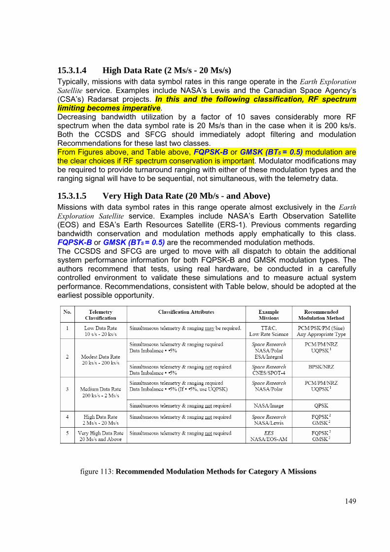
149
15.3.1.4 High Data Rate (2 Ms/s - 20 Ms/s) Typically, missions with data symbol rates in this range operate in the Earth Exploration Satellite service. Examples include NASA’s Lewis and the Canadian Space Agency’s (CSA’s) Radarsat projects. In this and the following classification, RF spectrum limiting becomes imperative. Decreasing bandwidth utilization by a factor of 10 saves considerably more RF spectrum when the data symbol rate is 20 Ms/s than in the case when it is 200 ks/s. Both the CCSDS and SFCG should immediately adopt filtering and modulation Recommendations for these last two classes. From Figures above, and Table above, FQPSK-B or GMSK (BTS = 0.5) modulation are the clear choices if RF spectrum conservation is important. Modulator modifications may be required to provide turnaround ranging with either of these modulation types and the ranging signal will have to be sequential, not simultaneous, with the telemetry data.
15.3.1.5 Very High Data Rate (20 Mb/s - and Above) Missions with data symbol rates in this range operate almost exclusively in the Earth Exploration Satellite service. Examples include NASA’s Earth Observation Satellite (EOS) and ESA’s Earth Resources Satellite (ERS-1). Previous comments regarding bandwidth conservation and modulation methods apply emphatically to this class. FQPSK-B or GMSK (BTS = 0.5) are the recommended modulation methods. The CCSDS and SFCG are urged to move with all dispatch to obtain the additional system performance information for both FQPSK-B and GMSK modulation types. The authors recommend that tests, using real hardware, be conducted in a carefully controlled environment to validate these simulations and to measure actual system performance. Recommendations, consistent with Table below, should be adopted at the earliest possible opportunity.
figure 113: Recommended Modulation Methods for Category A Missions
150
GLOSSARY ARX II A Research and Development Earth Station Receiver, (Prototype for DSN Block V) BER Bit-Error-Rate Bi-φ Binary-Phase [Manchester] modulation BL Receiver phase-locked-loop’s bandwidth, expressed in Hz BPSK Bi-Phase Shift Keying [modulation method] BTB Bandwidth • Time Product Based on Bit-Period BTS Bandwidth • Time Product Based on Symbol-Period Category A Space Mission whose distance from Earth is less than 2 • 106
km CCSDS Consultative Committee for Space Data Systems DSN Deep Space Network DTTL Digital Transition Tracking Loop ESA European Space Agency ESOC ESA Operation Center (Darmstadt, Germany) ESTEC ESA Technical Center (Noordwijk, The Netherlands) FQPSK Feher QPSK [modulation method] GMSK Gaussian Minimum Shift Keying HP Hewlett Packard Hz Hertz k Kilo (1,000) kb/s Kilo Bits per Second kHz Kilo Hertz ks/s Kilo Symbols Per Second M Mega (1,000,000) MHZ Mega Hertz MAP Maximum A Posteriori MODEM Modulation-Demodulation MSK Minimum Shift Keying NRZ Non Return to Zero [format] OQPSK Offset QPSK [modulation method] PA Power Amplifier PCS Personal Communications System PM Phase Modulation PSK Phase Shift Keying PT Total Power [transmitted] QPSK Quadrature Phase Shift Keying [modulation method] SAW Surface Acoustic Wave [Filter] SER Symbol-Error-Rate SFCG Space Frequency Coordination Group SPW Cadence Design Systems Inc. Signal Processing Worksystem SRRC Square Root Raised Cosine [Filter] SSPA Solid State Power Amplifier Subpanel 1E CCSDS group concerned with RF and Modulation standards
151
16 8PSK MODULATION (Example implemented in mobile telephone network)
16.1 Introduction After GPRS, the next step in improving the GSM system data rate is to change the signal to a type that has greater bandwidth efficiency, i.e. more bits per second can be supported per unit bandwidth. This is most economically implemented throughout the existing GSM infrastructure when the new signal type has identical bandwidth occupancy characteristics to the original 0.3-GMSK signal. EDGE is a modulation scheme that is more bandwidth efficient than the Gaussian pre-filtered minimum shift keying (GMSK) modulation scheme used in the GSM standard. The technology defines a new physical layer of an 8-Phase-Shift-Keying modulation (8PSK), instead of Gaussian-Minimum-Shift Keying (GMSK). 8PSK enables each pulse to carry 3 bits of information per symbol versus GPRS/GMSK’s 1 bit per symbol per pulse rate. Thus, it has the potential to increase the data rate of existing GSM system by a factor of three. For this reason, it requires a hardware upgrade of the RF part in the base stations and new mobile stations that support EDGE modulation. A traditional 8PSK system uses raised-cosine filtering to remove Inter-symbol Interference (ISI). Although ISI is eliminated by using raised-cosine filtering, (270 Ksymbol/s results in a channl bandwidth greater than 200 KHz) the 8PSK signal with rised-cosine filtering does not fit within 200 KHz of bandwidth. eq 256
In order to achieve the desired symbol rate using 200 KHz of bandwidth, a more severe filtering approach is required. 8PSK-EDGE makes this trade-off, resulting in a conservation of bandwidth versus the increase of ISI. This also necessitates a more complex design for the receiver.
( )
22.0_ 2002
KHz 330 1.22*2700001)/(2
12)/(
≅==
≅=+⋅=⇓
+=
factorrolloffrKhzB
rssymbolsDB
rBssymbolsD
EGPRS e GSM for instead where
filtering cosine raised a for
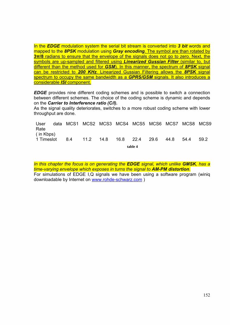
152
In the EDGE modulation system the serial bit stream is converted into 3 bit words and mapped to the 8PSK modulation using Gray encoding. The symbol are than rotated by 3π/8 radians to ensure that the envelope of the signals does not go to zero. Next, the symbols are up-sampled and filtered using Linearized Gussian Filter (similar to, but different than the method used for GSM). In this manner, the spectrum of 8PSK signal can be restricted to 200 KHz. Linearized Gussian Filtering allows the 8PSK signal spectrum to occupy the same bandwidth as a GPRS/GSM signals. It also introduces a considerable ISI component. EDGE provides nine different coding schemes and is possible to switch a connection between different schemes. The choice of the coding scheme is dynamic and depends on the Carrier to Interference ratio (C/I). As the signal quality deteriorates, switches to a more robust coding scheme with lower throughput are done. User data Rate ( in Kbps)
MCS1 MCS2 MCS3 MCS4 MCS5 MCS6 MCS7 MCS8 MCS9
1 Timeslot 8.4 11.2 14.8 16.8 22.4 29.6 44.8 54.4 59.2 table 4
In this chapter the focus is on generating the EDGE signal, which unlike GMSK, has a time-varying envelope which exposes in turns the signal to AM-PM distortion. For simulations of EDGE I,Q signals we have been using a software program (winiq downloadable by Internet on www.rohde-schwarz.com )
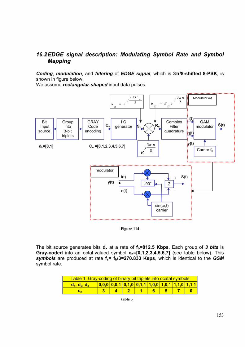
153
16.2 EDGE signal description: Modulating Symbol Rate and Symbol Mapping
Coding, modulation, and filtering of EDGE signal, which is 3π/8-shifted 8-PSK, is shown in figure below. We assume rectangular-shaped input data pulses.
Figure 114
The bit source generates bits dk at a rate of fb=812.5 Kbps. Each group of 3 bits is Gray-coded into an octal-valued symbol cn=[0,1,2,3,4,5,6,7] (see table below). This symbols are produced at rate fs= fb/3=270.833 Ksps, which is identical to the GSM symbol rate.
d1, d2, d3 0,0,0 0,0,1 0,1,0 0,1,1 1,0,0 1,0,1 1,1,0 1,1,1cn 3 4 2 1 6 5 7 0
Table 1. Gray-coding of binary bit triplets into ocatal symbols
table 5
Group into 3-bit
triplets
GRAY Code
encoding
I Q generator
Bit Input source
dk=[0,1] Cn =[0.1,2,3,4,5,6,7]
Complex Filter
quadrature
QAM modulatorCn Sn S(t)
83 nj
e⋅π y(t)
Carrier fc
Rn
82
nC
je
nS
π
=8
3 nje
nS
nR
π=
i(t)
q(t)
+ Σ
-
sin(ωct) carrier
-90°
i(t)
q(t)
S(t) y(t)
modulator
Modulator IQ
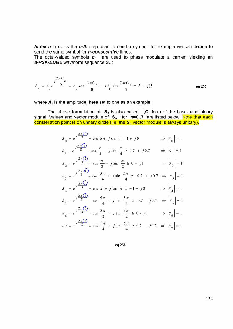
154
10.70.74
5sin4
5
11-02
3sin2
3
10.7--0.74
5sin4
5
101sin
10.7-0.74
3sin4
3
1102
sin2
10.70.74
sin4
1010sin
7cos8
727
6cos8
62
6
5cos8
52
5
4cos8
42
4
3cos8
32
3
2cos8
22
2
1cos8
12
1
00cos8
02
0
=⇒−≅+
=⇒≅+
=⇒≅+
=⇒+−≅+
=⇒+≅+
=⇒+≅+
=⇒+≅+
=⇒+=+
=⋅
=
=⋅
=
=⋅
=
=⋅
=
=⋅
=
=⋅
=
=⋅
=
=⋅
=
Sj
eS
Sj
eS
Sj
eS
Sj
eS
Sj
eS
Sj
eS
Sj
eS
Sj
eS
jj
jj
jj
jj
jj
jj
jj
jj
ππ
ππ
ππ
ππ
ππ
ππ
ππ
π
π
π
π
π
π
π
π
Index n in cn, is the n-th step used to send a symbol, for example we can decide to send the same symbol for n-consecutive times. The octal-valued symbols cn are used to phase modulate a carrier, yielding an 8-PSK-EDGE waveform sequence Sn :
jQICjC nnc
Ac
An
Cj
ec
An
S +=+==8
2sin8
2cos8
2ππ
π
eq 257
where Ac is the amplitude, here set to one as an example.
The above formulation of Sn is also called I,Q, form of the base-band binary signal. Values and vector module of Sn for n=0..7 are listed below. Note that each constellation point is on unitary circle (i.e. the Sn vector module is always unitary).
eq 258
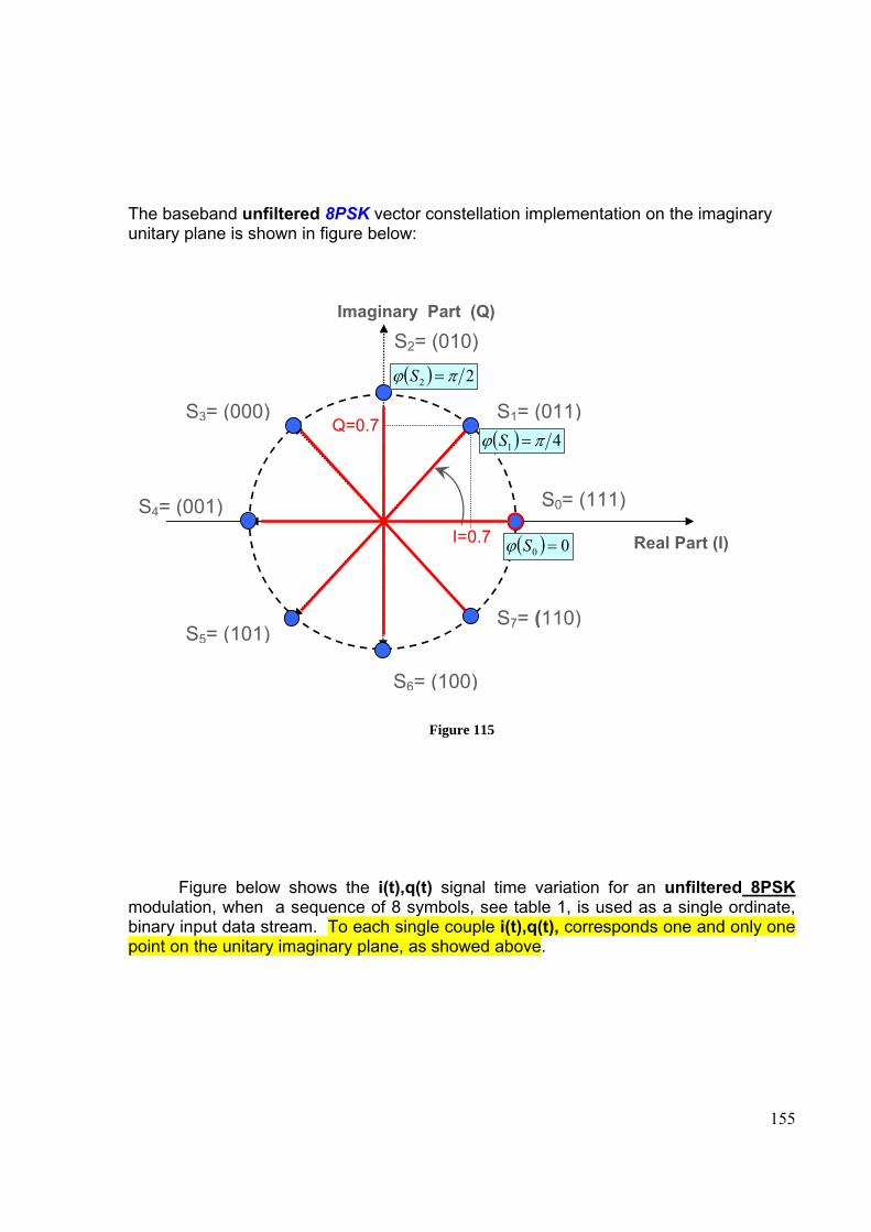
155
The baseband unfiltered 8PSK vector constellation implementation on the imaginary unitary plane is shown in figure below:
Figure 115
Figure below shows the i(t),q(t) signal time variation for an unfiltered 8PSK
modulation, when a sequence of 8 symbols, see table 1, is used as a single ordinate, binary input data stream. To each single couple i(t),q(t), corresponds one and only one point on the unitary imaginary plane, as showed above.
S0= (111)
S1= (011)
S2= (010)
S3= (000)
S4= (001)
S5= (101)
S6= (100)
S7= (110)
Real Part (I)
Imaginary Part (Q)
I=0.7
Q=0.7
( ) 00 =Sϕ
( ) 41 πϕ =S
( ) 22 πϕ =S
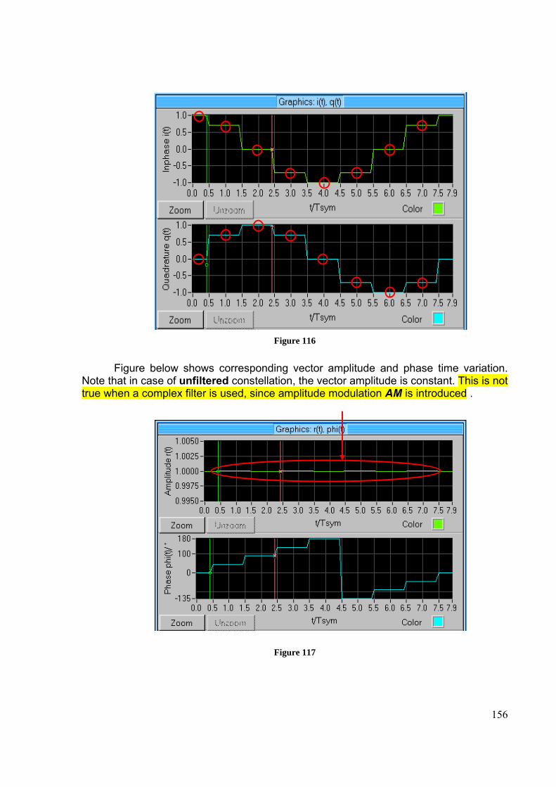
156
Figure 116
Figure below shows corresponding vector amplitude and phase time variation.
Note that in case of unfiltered constellation, the vector amplitude is constant. This is not true when a complex filter is used, since amplitude modulation AM is introduced .
Figure 117
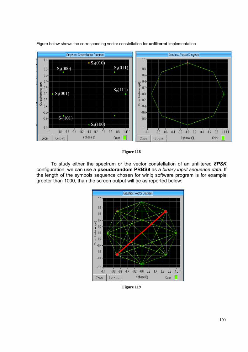
157
Figure below shows the corresponding vector constellation for unfiltered implementation.
Figure 118
To study either the spectrum or the vector constellation of an unfiltered 8PSK
configuration, we can use a pseudorandom PRBS9 as a binary input sequence data. If the length of the symbols sequence chosen for winiq software program is for example greeter than 1000, than the screen output will be as reported below:
Figure 119
S0(111)
S1(011) S3(000)
S4(001)
S5(101)
S2(010)
S6(100)
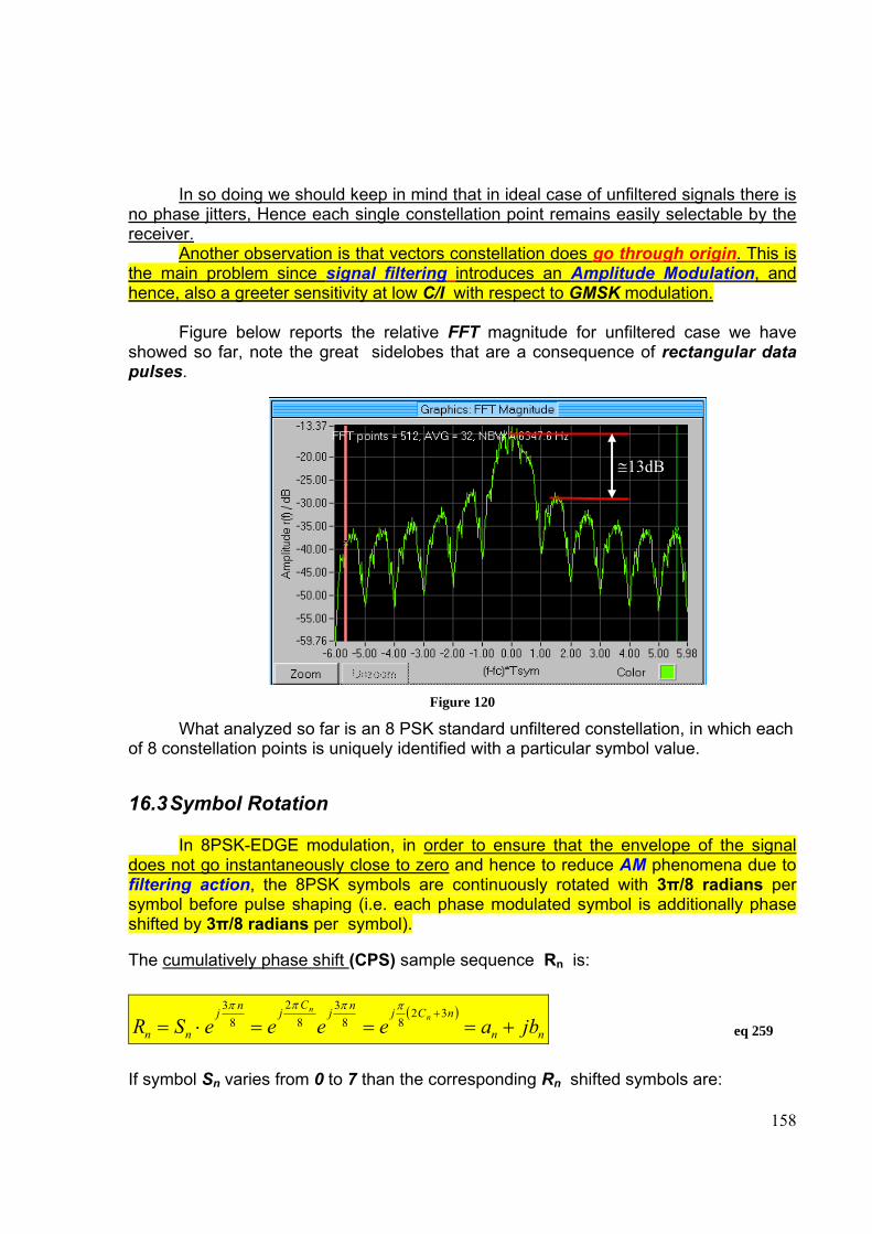
158
In so doing we should keep in mind that in ideal case of unfiltered signals there is
no phase jitters, Hence each single constellation point remains easily selectable by the receiver.
Another observation is that vectors constellation does go through origin. This is the main problem since signal filtering introduces an Amplitude Modulation, and hence, also a greeter sensitivity at low C/I with respect to GMSK modulation.
Figure below reports the relative FFT magnitude for unfiltered case we have
showed so far, note the great sidelobes that are a consequence of rectangular data pulses.
Figure 120
What analyzed so far is an 8 PSK standard unfiltered constellation, in which each of 8 constellation points is uniquely identified with a particular symbol value.
16.3 Symbol Rotation In 8PSK-EDGE modulation, in order to ensure that the envelope of the signal
does not go instantaneously close to zero and hence to reduce AM phenomena due to filtering action, the 8PSK symbols are continuously rotated with 3π/8 radians per symbol before pulse shaping (i.e. each phase modulated symbol is additionally phase shifted by 3π/8 radians per symbol).
The cumulatively phase shift (CPS) sample sequence Rn is:
( )nn
nCjn
jC
jn
j
nn jbaeeeeSR nn
+===⋅=+32
883
82
83 ππππ
eq 259
If symbol Sn varies from 0 to 7 than the corresponding Rn shifted symbols are:
≅13dB
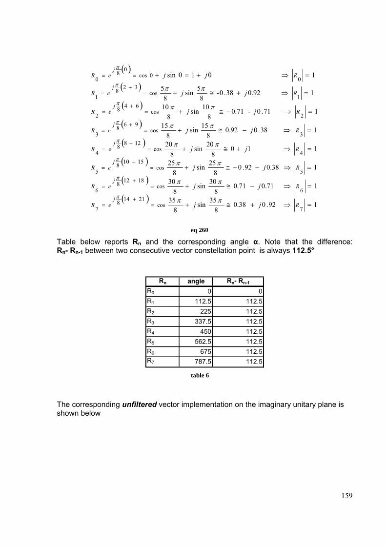
159
( )
( )
( )
( )
( )
( )
( )
( )192.00.38
835sin
835
10.710.718
30sin8
30
10.3892.08
25sin8
25
1108
20sin8
20
138.00.928
15sin8
15
171.0-0.718
10sin8
10
10.9238.0-8
5sin8
5
1010sin
7cos
211487
6cos
181286
5cos
151085
4cos
12884
3cos
9683
2cos
6482
1cos
3281
00cos
080
=⇒+≅+
=⇒−≅+
=⇒−−≅+
=⇒+≅+
=⇒−≅+
=⇒−≅+
=⇒+≅+
=⇒+=+
=+
=
=+
=
=+
=
=+
=
=+
=
=+
=
=+
=
==
Rj
eR
Rj
eR
Rj
eR
Rj
eR
Rj
eR
Rj
eR
Rj
eR
Rj
eR
jj
jj
jj
jj
jj
jj
jj
jj
ππ
ππ
ππ
ππ
ππ
ππ
ππ
π
π
π
π
π
π
π
π
eq 260
Table below reports Rn and the corresponding angle α. Note that the difference: Rn- Rn-1 between two consecutive vector constellation point is always 112.5°
Rn angle Rn- Rn-1
R0 0 0R1 112.5 112.5R2 225 112.5R3 337.5 112.5R4 450 112.5R5 562.5 112.5R6 675 112.5R7 787.5 112.5
table 6
The corresponding unfiltered vector implementation on the imaginary unitary plane is shown below
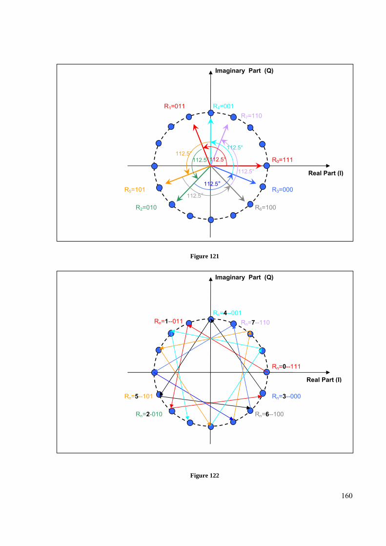
160
Figure 121
Figure 122
Real Part (I)
Rn=0--111
Rn=1--011
Rn=2-010
Rn=3--000
Rn=4--001
Rn=5--101
Rn=6--100
Rn=7--110
Imaginary Part (Q)
Real Part (I)
R0=111
R1=011
R2=010
R3=000
R4=001
R5=101
R6=100
R7=110
Imaginary Part (Q)
112.5° 112.5°
112.5°
112.5° 112.5°
112.5°
112.5°
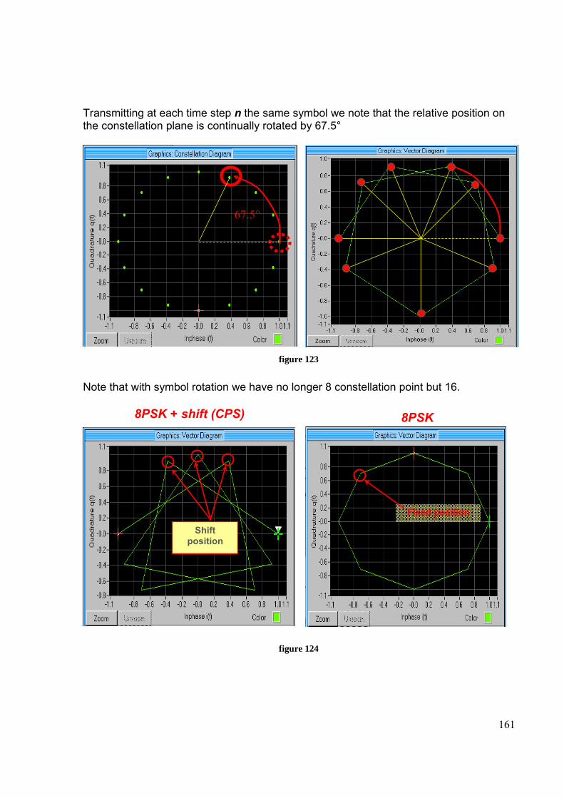
161
Transmitting at each time step n the same symbol we note that the relative position on the constellation plane is continually rotated by 67.5°
67.5°67.5°
figure 123
Note that with symbol rotation we have no longer 8 constellation point but 16.
figure 124
8PSK 8PSK + shift (CPS)
Fixed position
Shift position
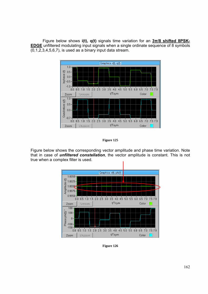
162
Figure below shows i(t), q(t) signals time variation for an 3π/8 shifted 8PSK-
EDGE unfiltered modulating input signals when a single ordinate sequence of 8 symbols (0,1,2,3,4,5,6,7), is used as a binary input data stream.
Figure 125
Figure below shows the corresponding vector amplitude and phase time variation. Note that in case of unfiltered constellation, the vector amplitude is constant. This is not true when a complex filter is used.
Figure 126
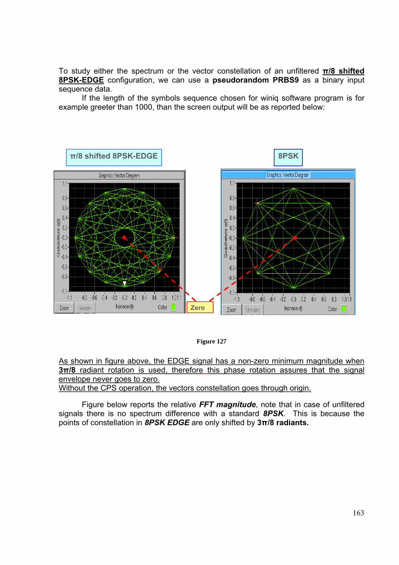
163
To study either the spectrum or the vector constellation of an unfiltered π/8 shifted 8PSK-EDGE configuration, we can use a pseudorandom PRBS9 as a binary input sequence data.
If the length of the symbols sequence chosen for winiq software program is for example greeter than 1000, than the screen output will be as reported below:
Figure 127
As shown in figure above, the EDGE signal has a non-zero minimum magnitude when 3π/8 radiant rotation is used, therefore this phase rotation assures that the signal envelope never goes to zero. Without the CPS operation, the vectors constellation goes through origin.
Figure below reports the relative FFT magnitude, note that in case of unfiltered signals there is no spectrum difference with a standard 8PSK. This is because the points of constellation in 8PSK EDGE are only shifted by 3π/8 radiants.
π/8 shifted 8PSK-EDGE 8PSK
Zero
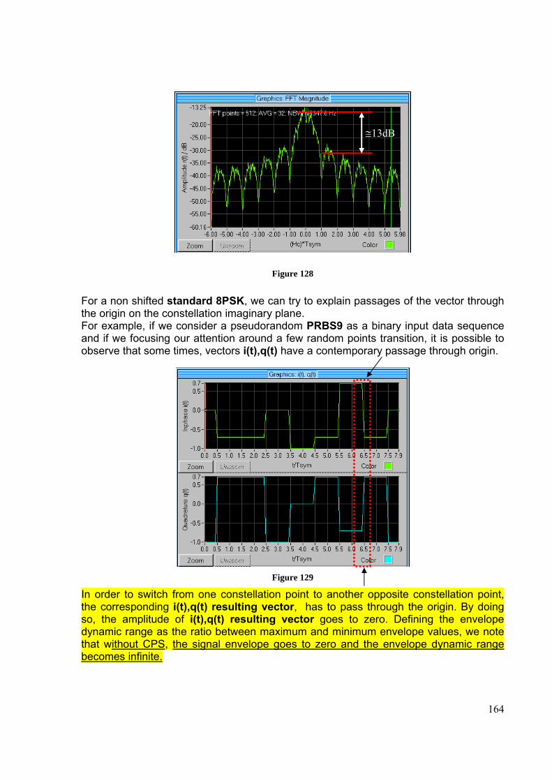
164
Figure 128
For a non shifted standard 8PSK, we can try to explain passages of the vector through the origin on the constellation imaginary plane. For example, if we consider a pseudorandom PRBS9 as a binary input data sequence and if we focusing our attention around a few random points transition, it is possible to observe that some times, vectors i(t),q(t) have a contemporary passage through origin.
Figure 129
In order to switch from one constellation point to another opposite constellation point, the corresponding i(t),q(t) resulting vector, has to pass through the origin. By doing so, the amplitude of i(t),q(t) resulting vector goes to zero. Defining the envelope dynamic range as the ratio between maximum and minimum envelope values, we note that without CPS, the signal envelope goes to zero and the envelope dynamic range becomes infinite.
≅13dB
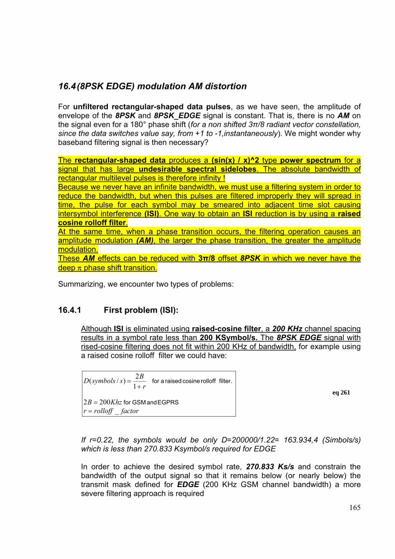
165
16.4 (8PSK EDGE) modulation AM distortion For unfiltered rectangular-shaped data pulses, as we have seen, the amplitude of envelope of the 8PSK and 8PSK_EDGE signal is constant. That is, there is no AM on the signal even for a 180° phase shift (for a non shifted 3π/8 radiant vector constellation, since the data switches value say, from +1 to -1,instantaneously). We might wonder why baseband filtering signal is then necessary? The rectangular-shaped data produces a (sin(x) / x)^2 type power spectrum for a signal that has large undesirable spectral sidelobes. The absolute bandwidth of rectangular multilevel pulses is therefore infinity ! Because we never have an infinite bandwidth, we must use a filtering system in order to reduce the bandwidth, but when this pulses are filtered improperly they will spread in time, the pulse for each symbol may be smeared into adjacent time slot causing intersymbol interference (ISI). One way to obtain an ISI reduction is by using a raised cosine rolloff filter. At the same time, when a phase transition occurs, the filtering operation causes an amplitude modulation (AM), the larger the phase transition, the greater the amplitude modulation. These AM effects can be reduced with 3π/8 offset 8PSK in which we never have the deep π phase shift transition. Summarizing, we encounter two types of problems:
16.4.1 First problem (ISI):
Although ISI is eliminated using raised-cosine filter, a 200 KHz channel spacing results in a symbol rate less than 200 KSymbol/s. The 8PSK EDGE signal with rised-cosine filtering does not fit within 200 KHz of bandwidth, for example using a raised cosine rolloff filter we could have:
factorrolloffrKhzB
rBssymbolsD
_ 2002
.12)/(
==
+=
EGPRS and GSM for
filter rolloff cosine raised a for eq 261
If r=0.22, the symbols would be only D=200000/1.22= 163.934,4 (Simbols/s) which is less than 270.833 Ksymbol/s required for EDGE
In order to achieve the desired symbol rate, 270.833 Ks/s and constrain the bandwidth of the output signal so that it remains below (or nearly below) the transmit mask defined for EDGE (200 KHz GSM channel bandwidth) a more severe filtering approach is required
166
The transmit filter used is a Linearized Gussian Filter (similar to, but different than the method used for GSM). In this manner, the spectrum of 8PSK signal can be restricted to 200 KHz and the symbols filtering allow the 8PSK signal spectrum to occupy the same bandwidth as a GPRS/GSM signals. In the same time it also introduces a considerable ISI component. Because of the severe ISI introduced by the linearized Gussian Filters, the receiver includes an equalizer, and the Signal-to-Noise Ratio on Co-channel interference of about C/N ≥ 18 dB is quite high if compared to a GMSK modulation where C/N ≥ 9 dB
Since the EDGE transmit mask is nearly identical to the GSM transmit mask, the EDGE signal succeeds in tripling the data throughput within the standard GSM channel.
16.4.2 Second problem (AM):
Filtering produces Amplitude Modulation AM on the resulting EDGE signal because the filtered data waveform cannot change instantaneously from one peak to another, especially if 180° phase transitions occur as in a simple 8PSK modulation. Although filtering solves the problem of poor spectral sidelobes, it creates another: AM on the EDGE signal. AM has several consequences:
• 8PSK EDGE constellations points are no longer on the unitary circle so amplitude jitter experienced by resulting vector occur in a more C/I sensitivity at receiver user side;
• Because (for the reason above), when EDGE modulation is used, the mean output transmitted power is lower compared to GSM modulation (about 2 dB). Than if BCCH (broadcast control channel) carrier is used for EDGE the cell-reselection-algorithm could experiences a fault.
• Due to AM, low-efficiency, linear (class A or class B) amplifiers, instead of high-efficiency non linear (class C) amplifiers, are required for the 8PSK signal without distortion. In portable communication applications, these amplifiers increase the battery capacity requirements.
These AM effects can be reduced with 3π/8 offset 8PSK in which we never have the π phase shift transition.
167
16.5 Used Gaussian EDGE Filter
The complex sequence Rn is next passed through a low-pass filter to produce the filtered complex signal.
∑ −⋅=n
n nTtpRtx )()( eq 262
where T=1/fs is the symbol interval, and p(t) is the filter pulse shape. We can rewrite in the alternative form:
∑∑ −⋅+−⋅=+=n
nn
n nTtpbjnTtpatjQtItx )()()()()( eq 263
with real symbol an, bn and real pulse p(t), for two real filtered signals I(t) and O(t). Each real filtered signals can be visualized as the output of a linear time-invariant (LTI) filter driven by a stream of impulse scaled by an, (or bn), yielding a linear superposition of
scaled time-shifted pulses p(t).
The exact filter pulses shape p(t) defined for EDGE signal is non-zero over the interval -5(T/2) ≤ t ≤ 5(T/2),
⎟⎠⎞
⎜⎝⎛ += Ttctp
25)( 0 eq 264
where c0 is the principal pulse in the Laurent decomposition of the 0.3-GMSK modulation,
( )⎪⎭
⎪⎬⎫
⎪⎩
⎪⎨⎧
≤≤+= ∏=
elsewhere
TtiTtftc i
0
50)(3
00 eq 265
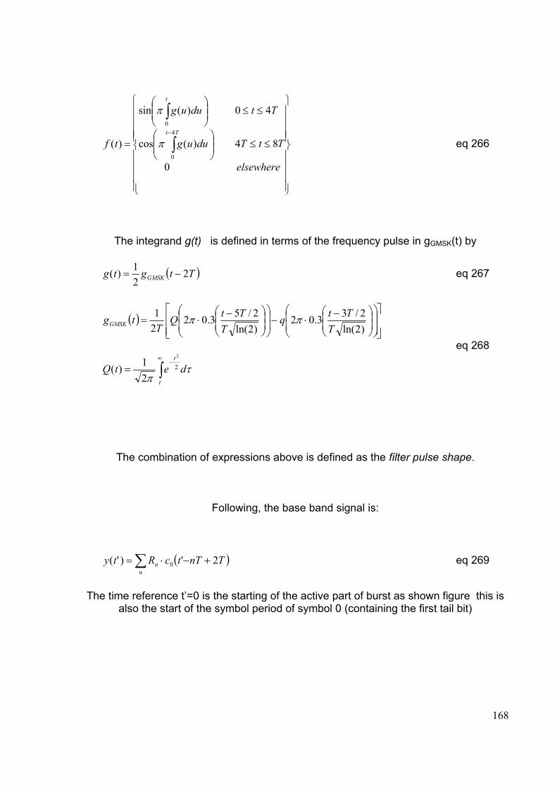
168
⎪⎪⎪⎪
⎭
⎪⎪⎪⎪
⎬
⎫
⎪⎪⎪⎪
⎩
⎪⎪⎪⎪
⎨
⎧
≤≤⎟⎟⎠
⎞⎜⎜⎝
⎛
≤≤⎟⎟⎠
⎞⎜⎜⎝
⎛
= ∫
∫−
elsewhere
TtTduug
Ttduug
tfTt
t
0
84)(cos
40)(sin
)(4
0
0
π
π
eq 266
The integrand g(t) is defined in terms of the frequency pulse in gGMSK(t) by
( )Ttgtg GMSK 221)( −= eq 267
( )
τπ
ππ
detQ
TTtq
TTtQ
Ttg
t
r
GMSK
∫∞
−=
⎥⎥⎦
⎤
⎢⎢⎣
⎡⎟⎟⎠
⎞⎜⎜⎝
⎛⎟⎟⎠
⎞⎜⎜⎝
⎛ −⋅−⎟
⎟⎠
⎞⎜⎜⎝
⎛⎟⎟⎠
⎞⎜⎜⎝
⎛ −⋅=
2
2
21)(
)2ln(2/33.02
)2ln(2/53.02
21
eq 268
The combination of expressions above is defined as the filter pulse shape.
Following, the base band signal is:
( )∑ +−⋅=n
n TnTtcRty 2')'( 0 eq 269
The time reference t’=0 is the starting of the active part of burst as shown figure this is also the start of the symbol period of symbol 0 (containing the first tail bit)
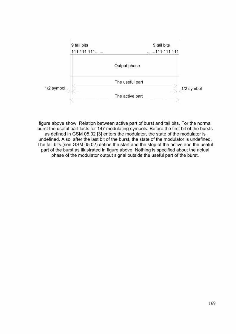
169
Output phase
The useful part
The active part
111 111 111....... .......111 111 1119 tail bits9 tail bits
1/2 symbol 1/2 symbol
figure above show Relation between active part of burst and tail bits. For the normal burst the useful part lasts for 147 modulating symbols. Before the first bit of the bursts
as defined in GSM 05.02 [3] enters the modulator, the state of the modulator is undefined. Also, after the last bit of the burst, the state of the modulator is undefined. The tail bits (see GSM 05.02) define the start and the stop of the active and the useful
part of the burst as illustrated in figure above. Nothing is specified about the actual phase of the modulator output signal outside the useful part of the burst.
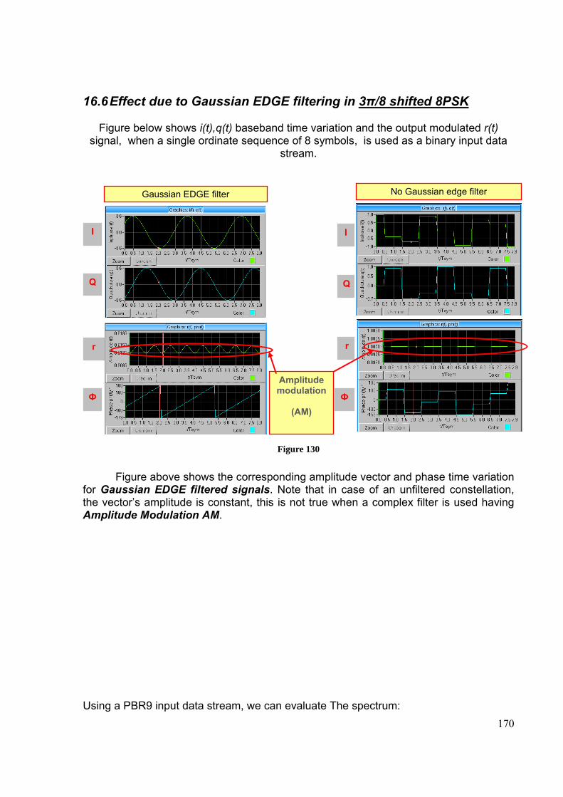
170
16.6 Effect due to Gaussian EDGE filtering in 3π/8 shifted 8PSK
Figure below shows i(t),q(t) baseband time variation and the output modulated r(t) signal, when a single ordinate sequence of 8 symbols, is used as a binary input data
stream.
Figure 130
Figure above shows the corresponding amplitude vector and phase time variation
for Gaussian EDGE filtered signals. Note that in case of an unfiltered constellation, the vector’s amplitude is constant, this is not true when a complex filter is used having Amplitude Modulation AM.
Using a PBR9 input data stream, we can evaluate The spectrum:
Amplitude modulation
(AM)
I
Q
r
Ф
I
Q
r
Ф
Gaussian EDGE filter No Gaussian edge filter
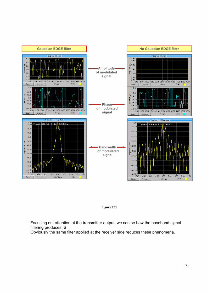
171
figure 131
Focusing out attention at the transmitter output, we can se haw the baseband signal filtering produces ISI. Obviously the same filter applied at the receiver side reduces these phenomena.
Amplitude of modulated
signal
Phase of modulated
signal
Bandwidth of modulated
signal
Gaussian EDGE filter No Gaussian EDGE filter
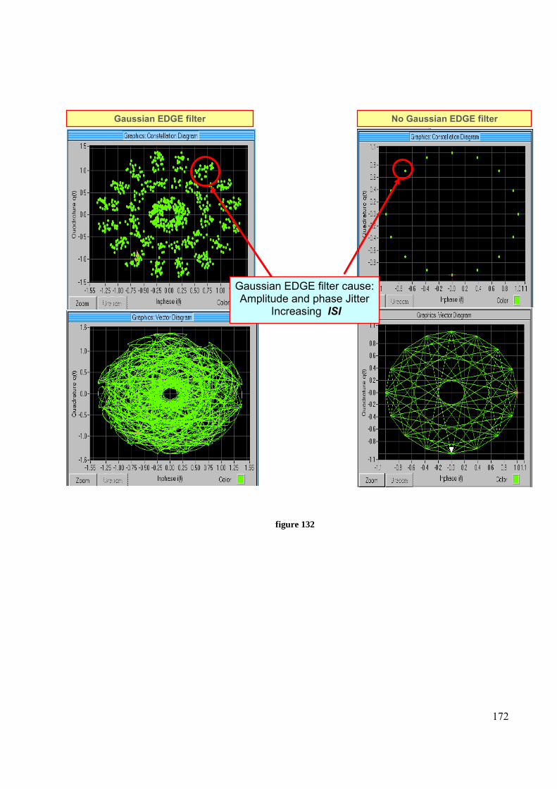
172
figure 132
Gaussian EDGE filter cause:Amplitude and phase Jitter
Increasing ISI
Gaussian EDGE filter No Gaussian EDGE filter
173
16.7 Modulation Let us indicate the frequency carrier fc. Follows that the QAM modulation is:
( ) ( )( )tjttyetyts cctj c ωωω sincos)(Re)(Re)( +⋅=⋅= eq 270
because y(t)=i(t)+jq(t) than the real part of output modulated signal becomes:
( ) ( ) ( )( )( )
ttqttits
ttqttjqttjittitjttjqtietyts
cc
cccc
cctj c
ωω
ωωωωωωω
sin)(cos)()(
sin)(cos)(sin)(cos)(Re sincos)()(Re)(Re)(
−=
=−++==+⋅+=⋅=
eq 271
using the filtering equation already seen before for a single burst:
( )∑ +−⋅=n
n TnTtcRty 2')'( 0 eq 272
the modulated RF carrier during the useful part of the burst became:
( )[ ]0'2)'(Re2)'( ϕπ +⋅= tfjs cetyTEts eq 273
where Es is the energy per modulating symbol, fc is the center frequency and φ0 is a random phase and is constant during one burst (see TS 05.04).
16.8 Conclusion The 3π/8 shifted 8PSK-EDGE signals succeeds in it’s primary goals of tripling the on-air data rate while maintaining nearly the same spectral occupancy as the original GSM signal. The 3π/8 shift assures that the signal envelope never falls below a certain level. Nonetheless, this signal has a significant envelope variation, which exposes the signal to AM-PM distortion impairments that don’t degrade the signal quality of GMSK.
174
17 EFFICIENT MODULATION METHODS STUDY AT NASA/JPL
17.1 PHASE SHIFT KEYED (8-PSK) MODULATION 8-PSK modulation is not currently used by CCSDS Space Agencies. Inserting a filter in the modulator further degrades system performance because non-orthogonality increases crosstalk between phase states.
17.2 PSK Modulation Bit-Error-Rate (BER) Losses are evident in Figure below showing the Bit-Error-Rate performance for 8-PSK modulation. Relative to ideal BPSK/NRZ modulation, even an ideal (lossless) 8-PSK system imposes heavy performance penalties. Ideal 8-PSK requires an EB / N0 of 9.5 - 10 dB to attain a BER = 1 x 10⁻³ When a Butterworth BTS = 3 filter is added, the required EB / N0 rises to 11.5 dB. Compared to the EB / N0 of about 8 dB, needed for a filtered non-ideal QPSK system at the same BER, it is clear that 8-PSK is not a useful modulation method in power limited applications. Losses using a Square Root Raised Cosine (r = 1) filter were so great that the plot is not even included in this report. Excessive losses result from the non-orthogonal relationship between phase states. This simulation shows that inherent 8-PSK modulation losses are unlikely to be acceptable in most applications, even without filtering.
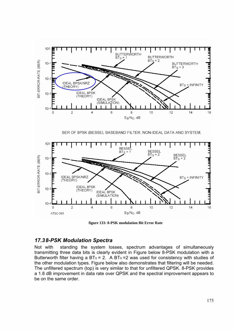
175
figure 133: 8-PSK modulation Bit Error Rate
17.3 8-PSK Modulation Spectra Not with standing the system losses, spectrum advantages of simultaneously transmitting three data bits is clearly evident in Figure below 8-PSK modulation with a Butterworth filter having a BTS = 2. A BTS =2 was used for consistency with studies of the other modulation types. Figure below also demonstrates that filtering will be needed. The unfiltered spectrum (top) is very similar to that for unfiltered QPSK. 8-PSK provides a 1.8 dB improvement in data rate over QPSK and the spectral improvement appears to be on the same order.
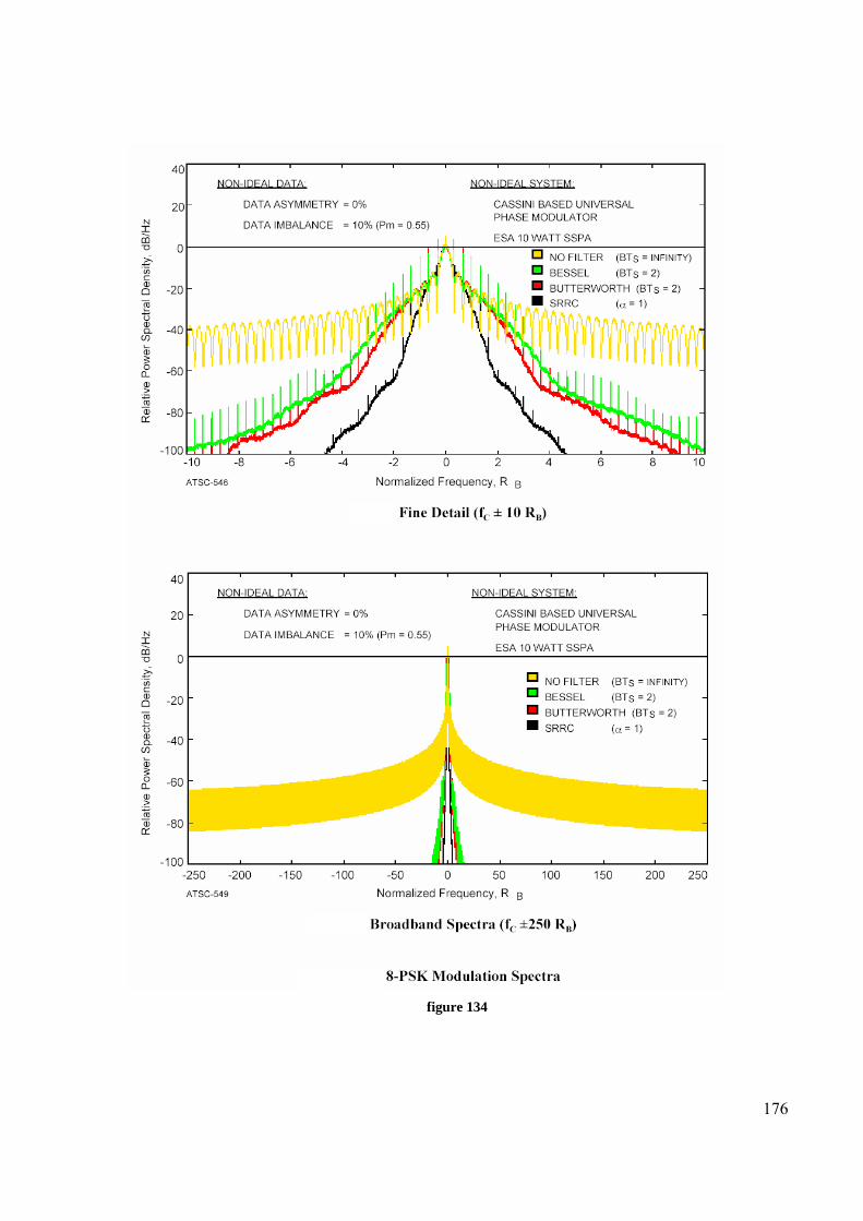
176
figure 134
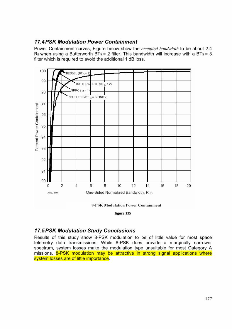
177
17.4 PSK Modulation Power Containment Power Containment curves, Figure below show the occupied bandwidth to be about 2.4 RB when using a Butterworth BTS = 2 filter. This bandwidth will increase with a BTS = 3 filter which is required to avoid the additional 1 dB loss.
figure 135
17.5 PSK Modulation Study Conclusions Results of this study show 8-PSK modulation to be of little value for most space telemetry data transmissions. While 8-PSK does provide a marginally narrower spectrum, system losses make the modulation type unsuitable for most Category A missions. 8-PSK modulation may be attractive in strong signal applications where system losses are of little importance.
178
18 MINIMUM-SHIFT KEYNG (MSK) AND GMSK MSK has the advantages of producing a constant-amplitude signal and, consequently, can be amplified with Class C amplifiers without distortion. As we will see, MSK is equivalent to OQPSK with sinusoidal pulse shaping [for hi(t)].
Definition: Minimum-shift keying (MSK) is a continuous-phase FSK with a minimum modulation index (h=0.5) that will produce orthogonal signalling.
First, let us shown that h=0.5 is the minimum index allowed for orthogonal continuous-phase FSK.
For the binary 1 to be transmitted over the bit interval 0<t<Tb, the FSK signal would be :
)cos()( 111 θω += tAts c eq 274
and for 0 to be transmitted the FSK signal would be
)cos()( 222 θω += tAts c eq 275
where θ1=θ2 for the continuous phase condition at the switching time t=0. For orthogonal signaling, we require the integral of the product of the two signals over the bit period 2Tb to be zero. Thus, we require:
[ ] [ ]
[ ] [ ]
[ ] [ ]
[ ]
[ ]
[ ] [ ] 0)()(sin21
)(1)()(sin
21
)(1
)()(cos21)(
)(1
)()(cos21)(
)(1
)()(cos)()(
21 )()(cos
)()(
21
)()(cos)()(
21)()(cos
)()(
21
)()(cos21)()(cos
21
i.e. 0)cos()cos()()(
2
02121
21
22
02121
21
2
2
0212121
2
21
2
2
0212121
21
2
2
02121
21
2122
02121
21
212
2
02121
21
212121
21
212
2
021212121
2
2
0
2
02211
221
=⎥⎦⎤
⎢⎣⎡ −+−
−+⎥⎦
⎤⎢⎣⎡ +++
+=
=⎥⎦⎤
⎢⎣⎡ −+−−
−+
+⎥⎦⎤
⎢⎣⎡ ++++
+=
=⎥⎦
⎤⎢⎣
⎡−+−
−−
+⎥⎦
⎤⎢⎣
⎡+++
++
=
=⎥⎦
⎤⎢⎣
⎡−+−
−−
++++++
=
=⎥⎦⎤
⎢⎣⎡ −+−++++=
=++=
∫
∫
∫∫
∫
∫
∫ ∫
Tb
c
Tb
c
Tb
cc
Tb
c
Tb
c
Tb
c
Tb
c
Tb
c
Tb Tb
c
tAtA
dttAA
dttA
dttAdttA
dtttA
dtttA
dtttAdttsts
θθωωωω
θθωωωω
θθωωωωωω
θθωωωωωω
θθωωωωωωθθωω
ωωωω
θθωωωωωω
θθωωωωωω
θθωωθθωω
θωθω
179
[ ] [ ]
[ ] [ ] 0)(sin21)(2)(sin
21
)(1
)(sin21)(2)(sin
21
)(1)()(
21212121
2
21212121
22
021
=⎥⎦⎤
⎢⎣⎡ −−−+−
−+
+⎥⎦⎤
⎢⎣⎡ +−+++
+=∫
θθθθωωωω
θθθθωωωω
bc
bc
Tb
TA
TAtdtsts eq 276
The first term is negligible, because (ω1+ω2) is large, so the requirements reduces to
[ ] [ ] 0)(sin)()(2sin2
)()(21
21212122
021 =⎥
⎦
⎤⎢⎣
⎡−
−−−+−=∫ ωω
θθθθωω bcTb TAtdtsts eq 277
for the continuous phase case the phase must be θ1=θ2; and the equation above is satisfied (i.e. equal to zero) for a minimum value h=0.5 .
in fact [ ] [ ] 0)(sin)()(2sin 212121 =−−−+− θθθθωω bT is verified when
⇒=− )(2 21 πωω bT [ ] [ ] 212121 when 0)(sin)(sin θθθθθθπ ==−−−+
but 21
21)( 2 )( 22 )(2 212121 hTffTffT bbb =⇒=−⇒=−⋅⇒=− πππωω
Therefore calling the modulation index h as:
( ) ( ) ( )πθ
πω
πωω ∆
=⋅∆
=−
=∆=−=2
2222 21
21bb
bbTTTfTffh then when
( ) ( )
22
212
41f
212 2/1 2121
πϑπϑ
=∆⇒=∆
=−=∆⇒=−=b
b TffTffh
eq 278
i.e. the peak to peak phase variation is 90° while the peak to peak frequency shift is ¼ Tb.
Now we will demonstrate that MSK signal is also a form OQPSK with sinusoidal pulse shaping. First, consider the FSK signal over the signalling interval (0,Tb). Then using
equation:
])(Re[)( tj cetgts ω= eq 279
the complex envelope is:
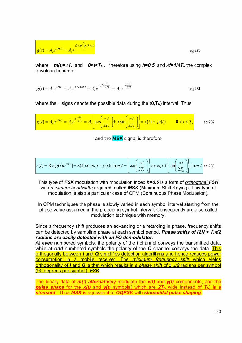
180
∫==
∆t
dmfj
ctj
c eAeAtg 0
)(2)()(
λλπθ eq 280
where m(t)=±1, and 0<t<Tb , therefore using h=0.5 and ∆f=1/4Tb the complex envelope became:
Tbtj
c
tTb
j
ctfj
ctj
c eAeAeAeAtg 24122)()(
πππθ ±±⋅∆± ==== eq 281
where the ± signs denote the possible data during the (0,Tb) interval. Thus,
bbb
cTbtj
ctj
c TttjytxTtj
TtAeAeAtg <<±=⎥
⎦
⎤⎢⎣
⎡⎟⎟⎠
⎞⎜⎜⎝
⎛±⎟⎟
⎠
⎞⎜⎜⎝
⎛===
±0 ),()(
2sin
2cos)( 2)( πππ
θ eq 282
and the MSK signal is therefore
tTtt
Ttttyttxetgts c
bc
bcc
tj c ωπωπωωω sin2
sincos2
cossin)(cos)(])(Re[)( ⎥⎦
⎤⎢⎣
⎡⎟⎟⎠
⎞⎜⎜⎝
⎛⎥⎦
⎤⎢⎣
⎡⎟⎟⎠
⎞⎜⎜⎝
⎛=−== m eq 283
This type of FSK modulation with modulation index h=0.5 is a form of orthogonal FSK with minimum bandwidth required, called MSK (Minimum Shift Keying). This type of
modulation is also a particular case of CPM (Continuous Phase Modulation).
In CPM techniques the phase is slowly varied in each symbol interval starting from the phase value assumed in the preceding symbol interval. Consequently are also called
modulation technique with memory.
Since a frequency shift produces an advancing or a retarding in phase, frequency shifts can be detected by sampling phase at each symbol period. Phase shifts of (2N + 1)π/2 radians are easily detected with an I/Q demodulator. At even numbered symbols, the polarity of the I channel conveys the transmitted data, while at odd numbered symbols the polarity of the Q channel conveys the data. This orthogonally between I and Q simplifies detection algorithms and hence reduces power consumption in a mobile receiver. The minimum frequency shift which yields orthogonality of I and Q is that which results in a phase shift of ± π/2 radians per symbol (90 degrees per symbol). FSK The binary data of m(t) alternatively modulate the x(t) and y(t) components, and the pulse shape for the x(t) and y(t) symbols( which are 2Tb wide instead of Tb) is a sinusoid. Thus MSK is equivalent to OQPSK with sinusoidal pulse shaping.
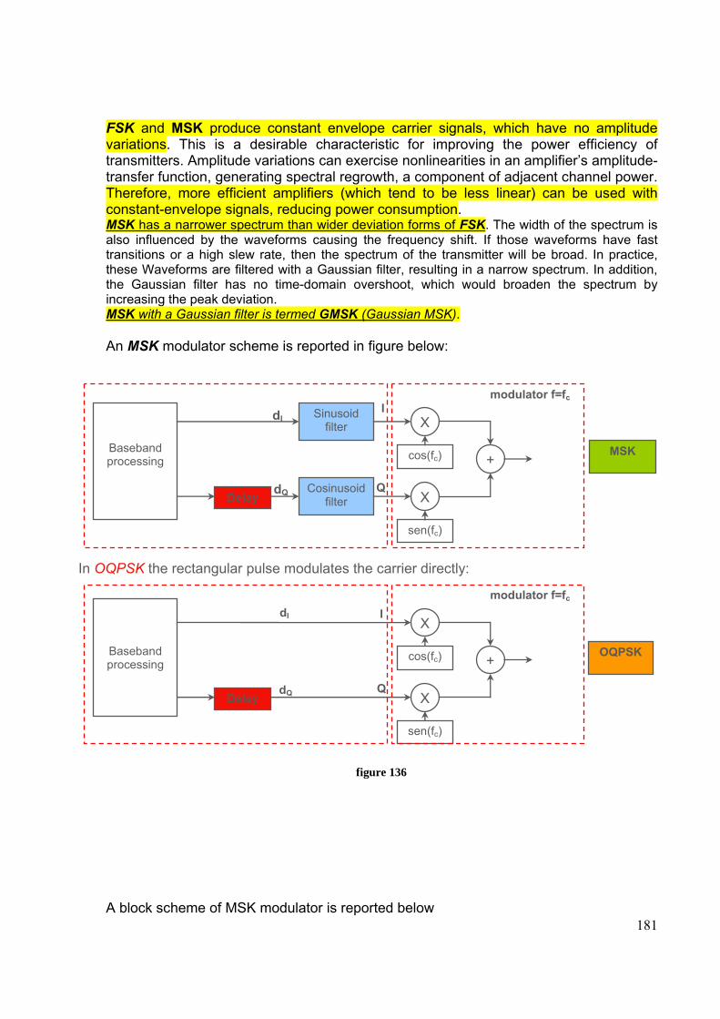
181
FSK and MSK produce constant envelope carrier signals, which have no amplitude variations. This is a desirable characteristic for improving the power efficiency of transmitters. Amplitude variations can exercise nonlinearities in an amplifier’s amplitude-transfer function, generating spectral regrowth, a component of adjacent channel power. Therefore, more efficient amplifiers (which tend to be less linear) can be used with constant-envelope signals, reducing power consumption. MSK has a narrower spectrum than wider deviation forms of FSK. The width of the spectrum is also influenced by the waveforms causing the frequency shift. If those waveforms have fast transitions or a high slew rate, then the spectrum of the transmitter will be broad. In practice, these Waveforms are filtered with a Gaussian filter, resulting in a narrow spectrum. In addition, the Gaussian filter has no time-domain overshoot, which would broaden the spectrum by increasing the peak deviation. MSK with a Gaussian filter is termed GMSK (Gaussian MSK). An MSK modulator scheme is reported in figure below:
figure 136
A block scheme of MSK modulator is reported below
In OQPSK the rectangular pulse modulates the carrier directly:
MSK
Delay
Sinusoid filter
Cosinusoid filter
X
X
+cos(fc)
sen(fc)
I
Q
Baseband processing
dI
dQ
modulator f=fc
OQPSK
Delay
X
X
+cos(fc)
sen(fc)
I
Q
dI
dQ
modulator f=fc
Baseband processing
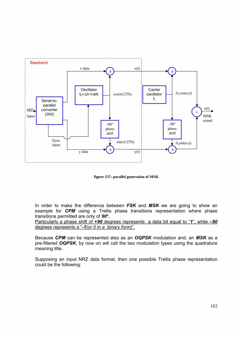
182
figure 137: parallel generation of MSK
In order to make the difference between FSK and MSK we are going to show an example for CPM using a Trellis phase transitions representation where phase transitions permitted are only of 90°. Particularly a phase shift of +90 degrees represents a data bit equal to “1”, while –90 degrees represents a “-1(or 0 in a binary form)”. Because CPM can be represented also as an OQPSK modulation and, an MSK as a pre-filtered OQPSK, by now on will call the two modulation types using the quadrature meaning title. Supposing an input NRZ data format, then one possible Trellis phase representation could be the following:
Serial-to-parallel
converter (2bit)
-90° phase shift
Oscillator f0=∆f=1/4R
Carrier oscillator
fc
-90° phase shift
X
X X
X
+
Sync input
y data
x data
y(t)
x(t)
s(t)
MSK signal
m(t)
input
cos(πt/2Tb)
sin(πt/2Tb)
Accos(ωct)
Acsin(ωct)
Baseband
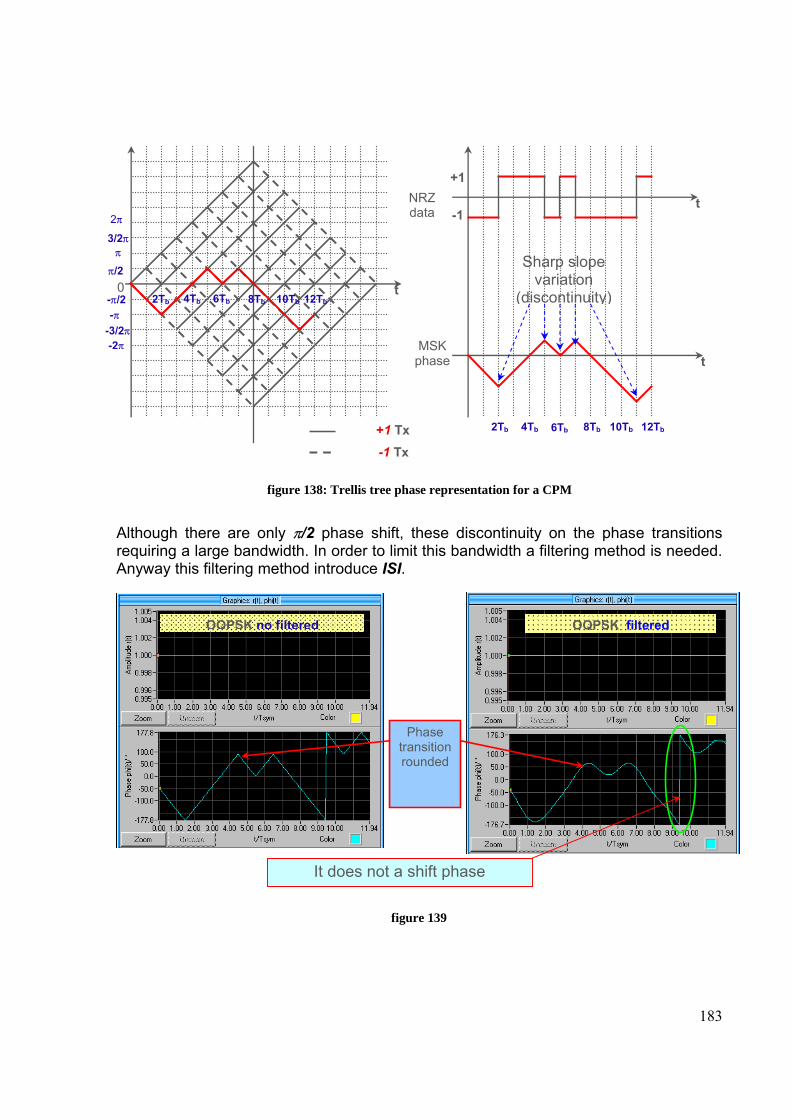
183
figure 138: Trellis tree phase representation for a CPM
Although there are only π/2 phase shift, these discontinuity on the phase transitions requiring a large bandwidth. In order to limit this bandwidth a filtering method is needed. Anyway this filtering method introduce ISI.
figure 139
NRZ data
t
t
t
-1
+1
MSK phase
0 2Tb 4Tb 6Tb 8Tb 10Tb 12Tb
2Tb 4Tb 6Tb 8Tb 10Tb 12Tb
-π/2
-π
-3/2π-2π
π/2π
3/2π
2π
+1 Tx
Sharp slope variation
(discontinuity)
-1 Tx
OQPSK no filtered OQPSK filtered
Phase transition rounded
It does not a shift phase
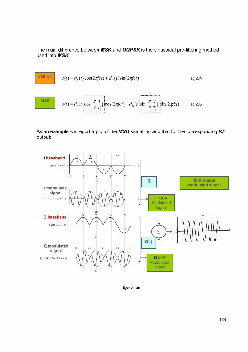
184
The main difference between MSK and OQPSK is the sinusoidal pre-filtering method used into MSK:
)2sin()()2cos()()( tfctdtfctdts QI ππ += eq 284
)2sin(2
sin)()2cos(2
cos)()( tfcTttdtfc
Tttdts
bQ
bI ππππ
⎥⎦
⎤⎢⎣
⎡+⎥
⎦
⎤⎢⎣
⎡= eq 285
As an example we report a plot of the MSK signalling and that for the corresponding RF output:
figure 140
I(t)
Q(t)
I MSK Modulated
signal
Q MSK Modulated
signal
Σ
MSK output modulated signal
I baseband
Q baseband
Q modulated signal
I modulated signal
OQPSK
MSK
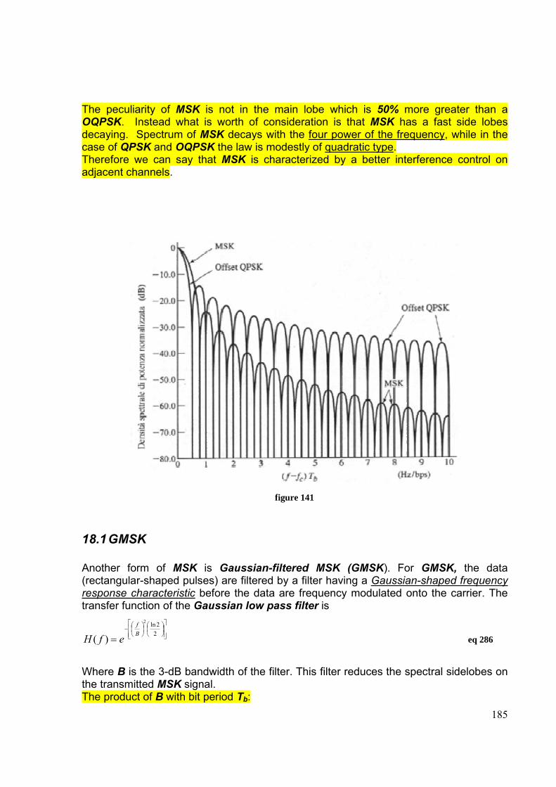
185
The peculiarity of MSK is not in the main lobe which is 50% more greater than a OQPSK. Instead what is worth of consideration is that MSK has a fast side lobes decaying. Spectrum of MSK decays with the four power of the frequency, while in the case of QPSK and OQPSK the law is modestly of quadratic type. Therefore we can say that MSK is characterized by a better interference control on adjacent channels.
figure 141
18.1 GMSK Another form of MSK is Gaussian-filtered MSK (GMSK). For GMSK, the data (rectangular-shaped pulses) are filtered by a filter having a Gaussian-shaped frequency response characteristic before the data are frequency modulated onto the carrier. The transfer function of the Gaussian low pass filter is
⎥⎥⎦
⎤
⎢⎢⎣
⎡⎟⎠⎞
⎜⎝⎛
⎟⎠⎞
⎜⎝⎛−
=22ln2
)( Bf
efH eq 286
Where B is the 3-dB bandwidth of the filter. This filter reduces the spectral sidelobes on the transmitted MSK signal. The product of B with bit period Tb:
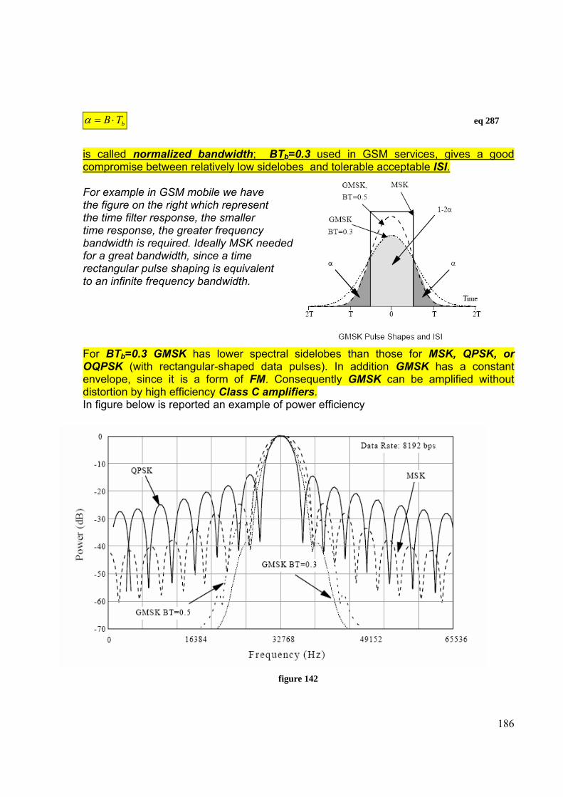
186
bTB ⋅=α eq 287
is called normalized bandwidth; BTb=0.3 used in GSM services, gives a good compromise between relatively low sidelobes and tolerable acceptable ISI. For example in GSM mobile we have the figure on the right which represent the time filter response, the smaller time response, the greater frequency bandwidth is required. Ideally MSK needed for a great bandwidth, since a time rectangular pulse shaping is equivalent to an infinite frequency bandwidth.
For BTb=0.3 GMSK has lower spectral sidelobes than those for MSK, QPSK, or OQPSK (with rectangular-shaped data pulses). In addition GMSK has a constant envelope, since it is a form of FM. Consequently GMSK can be amplified without distortion by high efficiency Class C amplifiers. In figure below is reported an example of power efficiency
figure 142
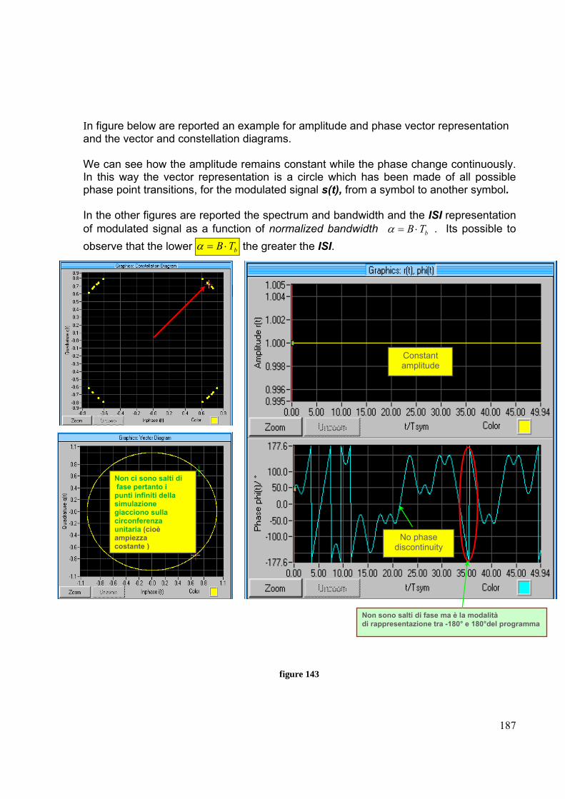
187
In figure below are reported an example for amplitude and phase vector representation and the vector and constellation diagrams. We can see how the amplitude remains constant while the phase change continuously. In this way the vector representation is a circle which has been made of all possible phase point transitions, for the modulated signal s(t), from a symbol to another symbol. In the other figures are reported the spectrum and bandwidth and the ISI representation of modulated signal as a function of normalized bandwidth bTB ⋅=α . Its possible to observe that the lower bTB ⋅=α the greater the ISI.
figure 143
No phase discontinuity
Constant amplitude
Non sono salti di fase ma è la modalità di rappresentazione tra -180° e 180°del programma
Non ci sono salti di fase pertanto i punti infiniti della simulazione giacciono sulla circonferenza unitaria (cioè ampiezza costante )
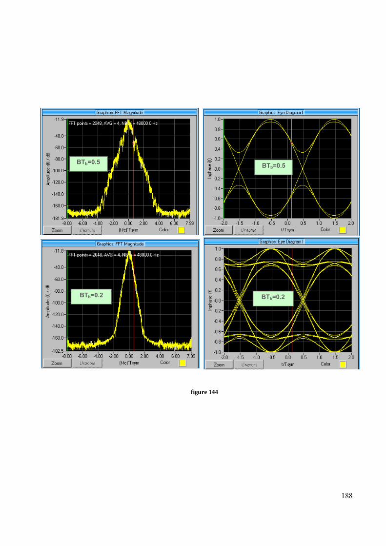
188
figure 144
BTb=0.5
BTb=0.2
BTb=0.5
BTb=0.2
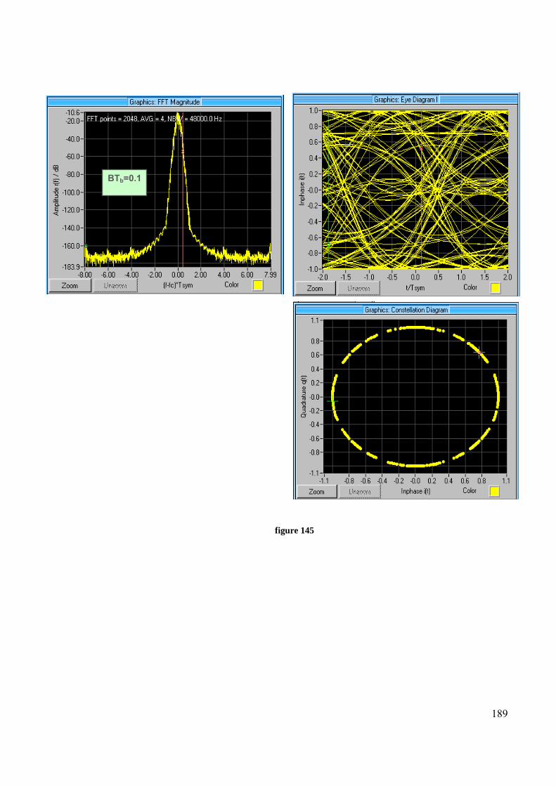
189
figure 145
BTb=0.1
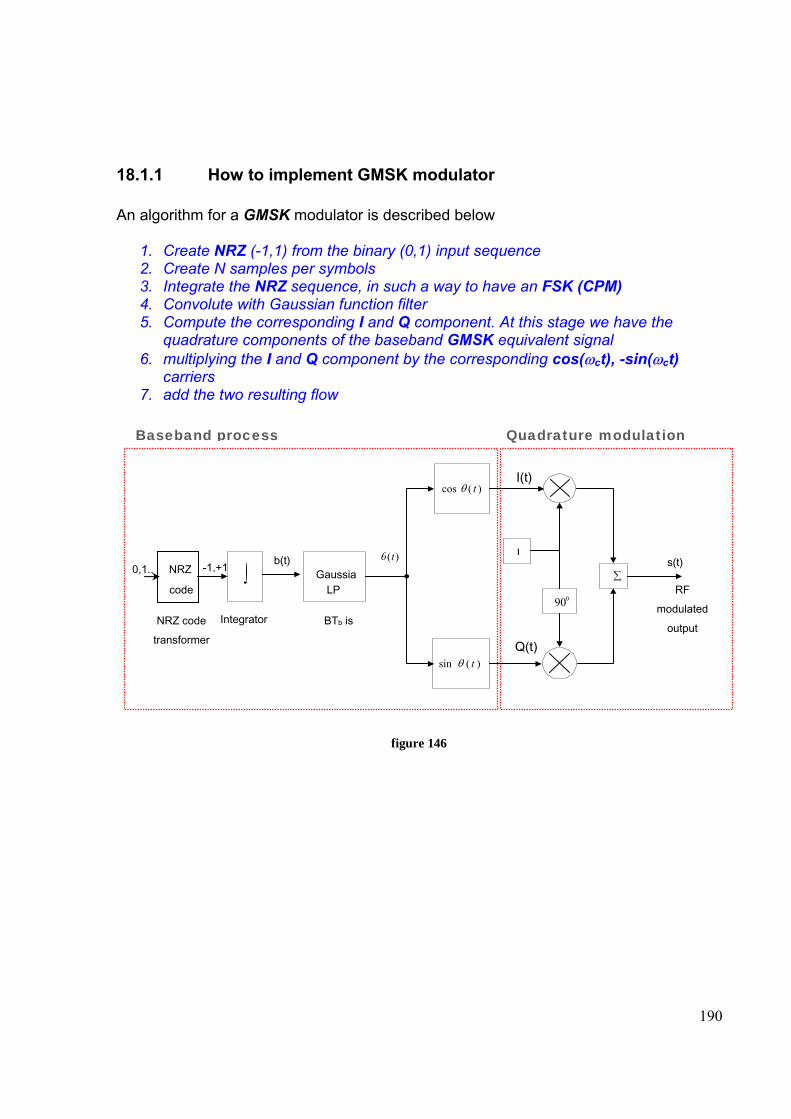
190
18.1.1 How to implement GMSK modulator An algorithm for a GMSK modulator is described below
1. Create NRZ (-1,1) from the binary (0,1) input sequence 2. Create N samples per symbols 3. Integrate the NRZ sequence, in such a way to have an FSK (CPM) 4. Convolute with Gaussian function filter 5. Compute the corresponding I and Q component. At this stage we have the
quadrature components of the baseband GMSK equivalent signal 6. multiplying the I and Q component by the corresponding cos(ωct), -sin(ωct)
carriers 7. add the two resulting flow
figure 146
Baseband process Quadrature modulation
GaussiaLP
∫NRZ code
BTb is Integrator
b(t) )(tθ
)(cos tθ
)(sin tθ
s(t) ∑
L
090
0,1.. -1,+1
I(t)
Q(t)
NRZ code transformer
RF modulated
output
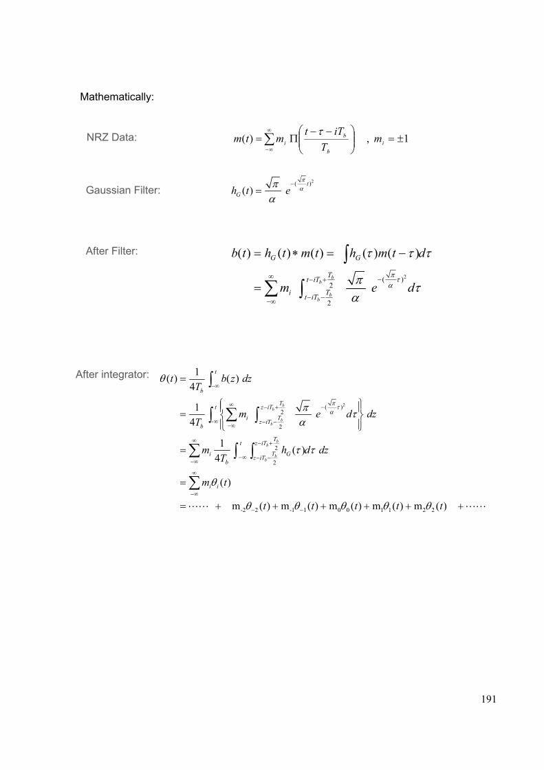
191
Mathematically:
1 , )( ±=⎟⎟⎠
⎞⎜⎜⎝
⎛ −−Π=∑
∞
∞−i
b
bi m
TiTt
mtmτ
2( )( )
t
Gh t eπαπ
α−
=
NRZ Data:
Gaussian Filter:
After Filter:
2( ) 2
2
( ) ( ) ( ) ( ) ( )
b
b
bb
G G
Tt iT
Ti t iT
b t h t m t h m t d
m e dπ τα
τ τ τ
π τα
∞ −− +
− −−∞
= ∗ = −
=
∫
∑ ∫
After integrator:
2
( ) 2
- 2
2
2
-2 2 -1 1 0 0 1 1 2 2
1( ) ( ) 4
1 4
1 ( ) 4
( )
m ( ) m ( ) m ( ) m ( ) m ( )
bb
bb
bb
bb
t
b
Tt z iT
Ti z iTb
Tt z iT
Ti Gz iTb
i i
t b z dzT
m e d dzT
m h d dzT
m t
t t t t t
π τα
θ
π τα
τ τ
θ
θ θ θ θ θ
−∞
∞ −− +
∞ − −−∞
∞ − +
−∞ − −−∞
∞
−∞
− −
=
⎧ ⎫⎪ ⎪= ⎨ ⎬⎪ ⎪⎩ ⎭
=
=
= + + + + +
∫
∑∫ ∫
∑ ∫ ∫
∑LL +LL
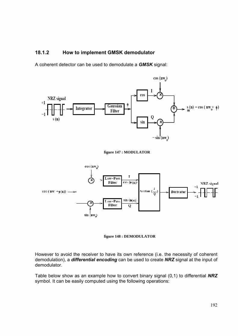
192
18.1.2 How to implement GMSK demodulator A coherent detector can be used to demodulate a GMSK signal:
figure 147 : MODULATOR
figure 148 : DEMODULATOR
However to avoid the receiver to have its own reference (i.e. the necessity of coherent demodulation), a differential encoding can be used to create NRZ signal at the input of demodulator. Table below show as an example how to convert binary signal (0,1) to differential NRZ symbol. It can be easily computed using the following operations:
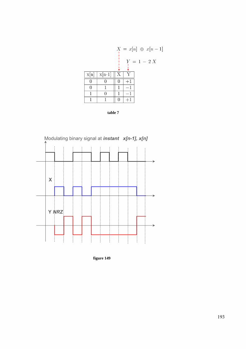
193
table 7
figure 149
Modulating binary signal at instant x[n-1], x[n]
X
Y NRZ
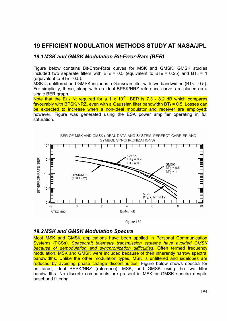
194
19 EFFICIENT MODULATION METHODS STUDY AT NASA/JPL
19.1 MSK and GMSK Modulation Bit-Error-Rate (BER) Figure below contains Bit-Error-Rate curves for MSK and GMSK. GMSK studies included two separate filters with BTS = 0.5 (equivalent to BTB = 0.25) and BTS = 1 (equivalent to BTB = 0.5). MSK is unfiltered and GMSK includes a Gaussian filter with two bandwidths (BTS = 0.5). For simplicity, these, along with an ideal BPSK/NRZ reference curve, are placed on a single BER graph. Note that the EB / N0 required for a 1 x 10⁻³ BER is 7.3 - 8.2 dB which compares favourably with BPSK/NRZ, even with a Gaussian filter bandwidth BTS = 0.5. Losses can be expected to increase when a non-ideal modulator and receiver are employed; however, Figure was generated using the ESA power amplifier operating in full saturation.
figure 150
19.2 MSK and GMSK Modulation Spectra Most MSK and GMSK applications have been applied in Personal Communication Systems (PCSs). Spacecraft telemetry transmission systems have avoided GMSK because of demodulation and synchronization difficulties. Often termed frequency modulation, MSK and GMSK were included because of their inherently narrow spectral bandwidths. Unlike the other modulation types, MSK is unfiltered and sidelobes are reduced by avoiding phase change discontinuities. Figure below shows spectra for unfiltered, ideal BPSK/NRZ (reference), MSK, and GMSK using the two filter bandwidths. No discrete components are present in MSK or GMSK spectra despite baseband filtering.
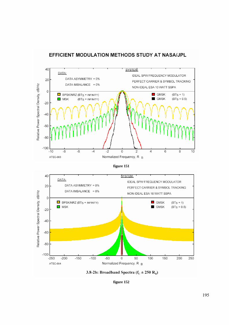
195
figure 151
figure 152
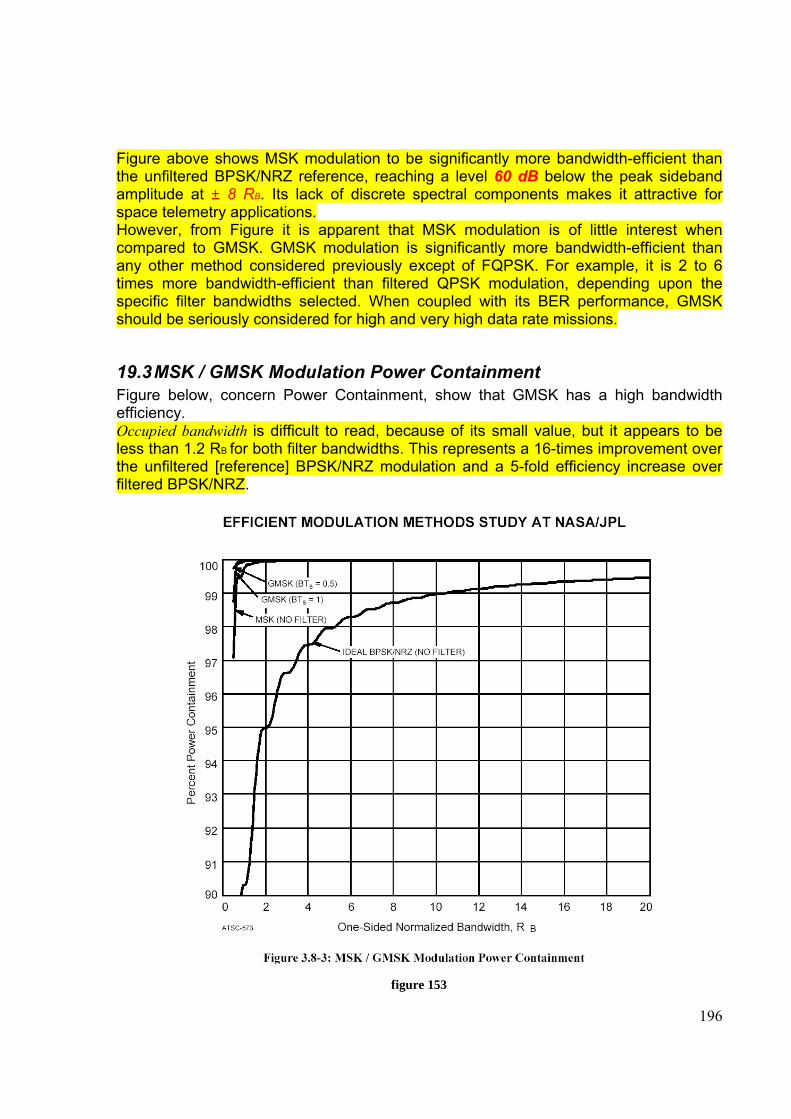
196
Figure above shows MSK modulation to be significantly more bandwidth-efficient than the unfiltered BPSK/NRZ reference, reaching a level 60 dB below the peak sideband amplitude at ± 8 RB. Its lack of discrete spectral components makes it attractive for space telemetry applications. However, from Figure it is apparent that MSK modulation is of little interest when compared to GMSK. GMSK modulation is significantly more bandwidth-efficient than any other method considered previously except of FQPSK. For example, it is 2 to 6 times more bandwidth-efficient than filtered QPSK modulation, depending upon the specific filter bandwidths selected. When coupled with its BER performance, GMSK should be seriously considered for high and very high data rate missions.
19.3 MSK / GMSK Modulation Power Containment Figure below, concern Power Containment, show that GMSK has a high bandwidth efficiency. Occupied bandwidth is difficult to read, because of its small value, but it appears to be less than 1.2 RB for both filter bandwidths. This represents a 16-times improvement over the unfiltered [reference] BPSK/NRZ modulation and a 5-fold efficiency increase over filtered BPSK/NRZ.
figure 153

197
19.4 MSK / GMSK Modulation Study Conclusions Clearly, space agencies interested in RF spectrum efficiency should seriously consider GMSK modulation. This is particularly true for high and very high data rate missions. Unlike the phase modulation types described above, GMSK requires new modulator, demodulator, and symbol synchronizer designs. In that respect, this recommendation departs from one of the Efficient Modulation Methods Study guidelines: that only simple modifications to existing Earth station equipment are permitted for any recommended modulation method. However, GMSK’s bandwidth efficiency is too great to be ignored and a departure from the guideline is warranted.
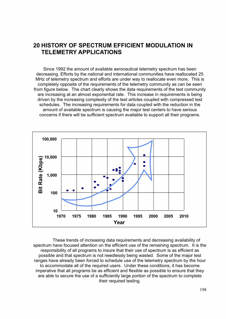
198
20 HISTORY OF SPECTRUM EFFICIENT MODULATION IN TELEMETRY APPLICATIONS
Since 1992 the amount of available aeronautical telemetry spectrum has been decreasing. Efforts by the national and international communities have reallocated 25 MHz of telemetry spectrum and efforts are under way to reallocate even more. This is completely opposite of the requirements of the telemetry community as can be seen
from figure below. The chart clearly shows the data requirements of the test community are increasing at an almost exponential rate. This increase in requirements is being driven by the increasing complexity of the test articles coupled with compressed test schedules. The increasing requirements for data coupled with the reduction in the
amount of available spectrum is causing the major test centers to have serious concerns if there will be sufficient spectrum available to support all their programs.
These trends of increasing data requirements and decreasing availability of spectrum have focused attention on the efficient use of the remaining spectrum. It is the
responsibility of all programs to insure that their use of spectrum is as efficient as possible and that spectrum is not needlessly being wasted. Some of the major test
ranges have already been forced to schedule use of the telemetry spectrum by the hour to accommodate all of the required users. Under these conditions, it has become
imperative that all programs be as efficient and flexible as possible to ensure that they are able to secure the use of a sufficiently large portion of the spectrum to complete
their required testing.
10
100
1,000
10,000
100,000
1970 1975 1980 1985 1990 1995 2000 2005 2010Year
Bit
Rat
e (K
bps)
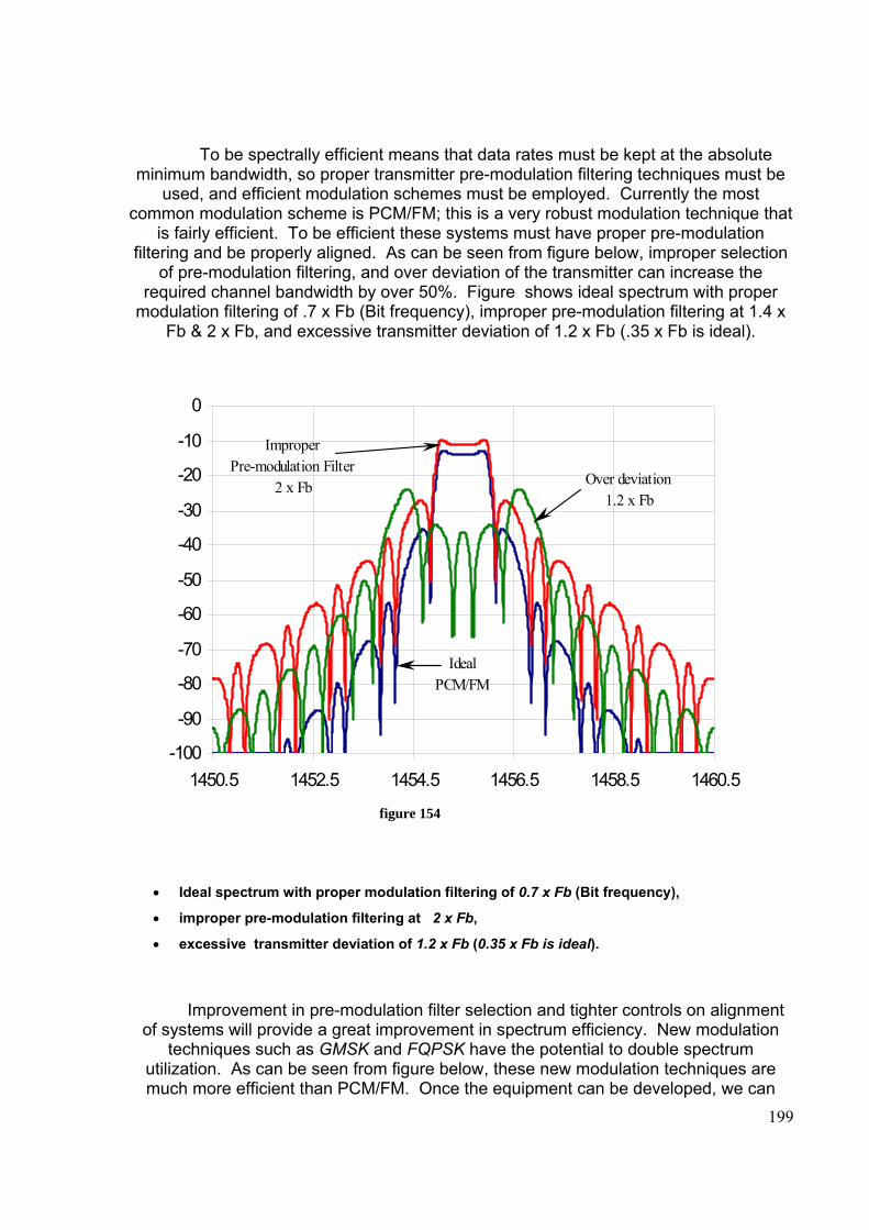
199
To be spectrally efficient means that data rates must be kept at the absolute minimum bandwidth, so proper transmitter pre-modulation filtering techniques must be
used, and efficient modulation schemes must be employed. Currently the most common modulation scheme is PCM/FM; this is a very robust modulation technique that
is fairly efficient. To be efficient these systems must have proper pre-modulation filtering and be properly aligned. As can be seen from figure below, improper selection
of pre-modulation filtering, and over deviation of the transmitter can increase the required channel bandwidth by over 50%. Figure shows ideal spectrum with proper
modulation filtering of .7 x Fb (Bit frequency), improper pre-modulation filtering at 1.4 x Fb & 2 x Fb, and excessive transmitter deviation of 1.2 x Fb (.35 x Fb is ideal).
figure 154
• Ideal spectrum with proper modulation filtering of 0.7 x Fb (Bit frequency),
• improper pre-modulation filtering at 2 x Fb,
• excessive transmitter deviation of 1.2 x Fb (0.35 x Fb is ideal).
Improvement in pre-modulation filter selection and tighter controls on alignment of systems will provide a great improvement in spectrum efficiency. New modulation
techniques such as GMSK and FQPSK have the potential to double spectrum utilization. As can be seen from figure below, these new modulation techniques are much more efficient than PCM/FM. Once the equipment can be developed, we can
-100
-90
-80
-70
-60
-50
-40
-30
-20
-10
0
1450.5 1452.5 1454.5 1456.5 1458.5 1460.5
Over deviation 1.2 x Fb
IdealPCM/FM
ImproperPre-modulation Filter
2 x Fb
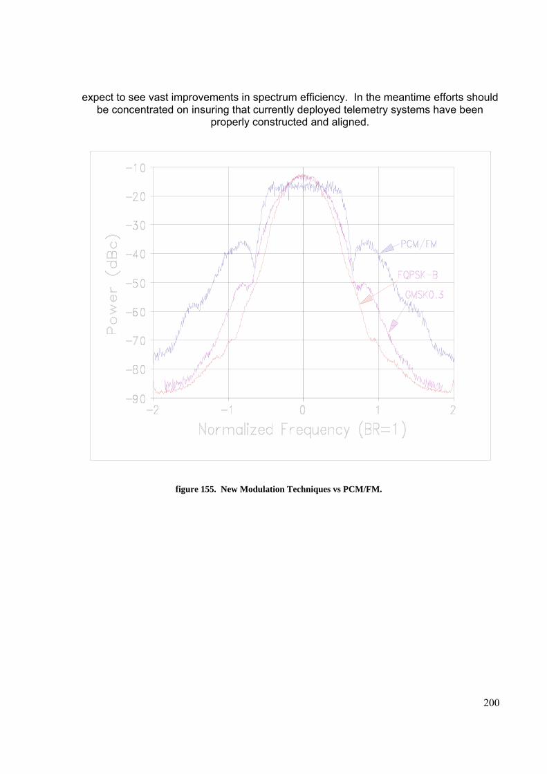
200
expect to see vast improvements in spectrum efficiency. In the meantime efforts should be concentrated on insuring that currently deployed telemetry systems have been
properly constructed and aligned.
figure 155. New Modulation Techniques vs PCM/FM.
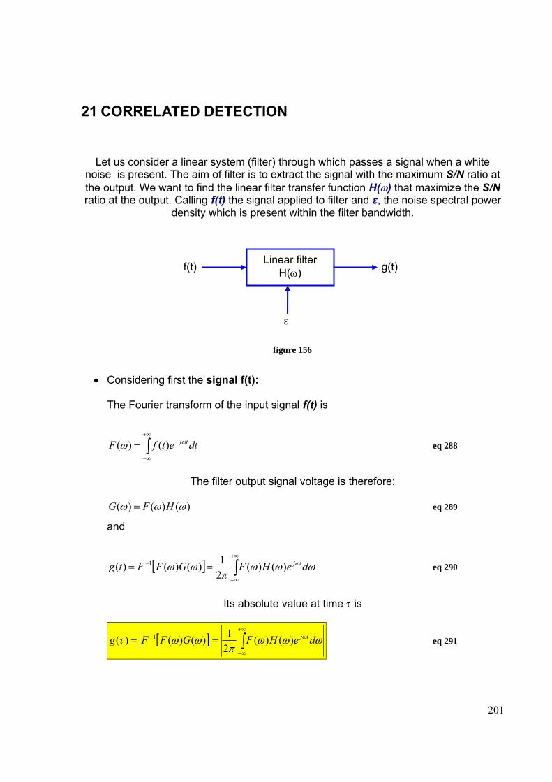
201
21 CORRELATED DETECTION
Let us consider a linear system (filter) through which passes a signal when a white noise is present. The aim of filter is to extract the signal with the maximum S/N ratio at the output. We want to find the linear filter transfer function H(ω) that maximize the S/N ratio at the output. Calling f(t) the signal applied to filter and ε, the noise spectral power
density which is present within the filter bandwidth.
figure 156
• Considering first the signal f(t):
The Fourier transform of the input signal f(t) is
∫+∞
∞−
−= dtetfF tjωω )()( eq 288
The filter output signal voltage is therefore:
)()()( ωωω HFG = eq 289
and
[ ] ωωωπ
ωω ω deHFGFFtg tj∫+∞
∞−
− == )()(21)()()( 1 eq 290
Its absolute value at time τ is
[ ] ωωωπ
ωωτ ω deHFGFFg tj∫+∞
∞−
− == )()(21)()()( 1 eq 291
Linear filter H(ω) f(t) g(t)
ε
202
let us consider now the noise
The filter input noise power spectral density is
2ε
=NoisePSD (W/Hz) eq 292
Where the spectrum is extended from positive to negative frequencies, then the filter output noise power spectral density will be
2)(2
)( ωεω HGN = eq 293
Where the filter Power spectrum is: 2)(ωH
The filter output noise power is therefore
∫+∞
∞−
= ωωεπ
dHPN2)(
221
eq 294
We want find H(ω) in order to maximize the output signal-to-noise ratio S/N:
⎟⎟⎠
⎞⎜⎜⎝
⎛
NPg )(max
2 τ where powersignal=)(2 τg
Ones the input signal is defined, it’s also defined its energy which is a constant given by
∫ ∫+∞
∞−
+∞
∞−
== ωωπ
dFdttfE 22 )(21)( eq 295
The signal to noise ratio, we want to maximize, can be divided by the energy E without altering the maximum S/N ratio determination. Therefore
⎪⎪
⎭
⎪⎪
⎬
⎫
⎪⎪
⎩
⎪⎪
⎨
⎧
⋅=
⎪⎪
⎭
⎪⎪
⎬
⎫
⎪⎪
⎩
⎪⎪
⎨
⎧
⋅=⎟⎟
⎠
⎞⎜⎜⎝
⎛⋅
∫ ∫
∫
∫ ∫
∫∞+
∞−
∞+
∞−
∞+
∞−∞+
∞−
∞+
∞−
∞+
∞−
ωωεωωπ
ωωω
ωωεπ
ωωπ
ωωωπτ
ωω
22
2
22
2
2
)(2
)(21
)()(max
)(22
1)(21
)()(21
max)(maxHdF
deHF
HdF
deHF
PEg
tjtj
N
eq 296
203
In order to maximize the preceding ratio we can use the Schwarz theorem for complex function integral:
∫∫∫+∞
∞−
+∞
∞−
+∞
∞−
⋅≤ ωωωωωωω dYdXdYX 222
)()()()( eq 297
The “=” sign is applied only when
)()( ωω ∗= kYX eq 298
so we have
∫∫∫+∞
∞−
+∞
∞−
+∞
∞−
⋅= ωωωωωωω dYdkYdYkY 22*
2
* )()()()( eq 299
Where Y*(.) is the conjugate complex value of Y(.)
Therefore calling:
tjeFYHX
ωωω
ωω
)()()()(
=
= eq 300
We can write
tj
tj
ekFHeiekFkYHX
ω
ω
ωω
ωωωω−
−
=
===
)()(..)()()()(
*
**
eq 301
Then substituting on the S/N ratio we can obtain the maximum value given by:
πε
ωωεππ
ωωπ
ωωεπ
ωωπ
ωωωωπ
ωωεπ
ωωπ
ωωωπτ
ω
4
1
)(22
121
)(21
max
)(22
1)(21
)()(21
max)(
221)(
21
)()(21
max)(max
22
22
22
22
22
2
2
=
⎪⎪
⎭
⎪⎪
⎬
⎫
⎪⎪
⎩
⎪⎪
⎨
⎧
=
⎪⎪⎭
⎪⎪⎬
⎫
⎪⎪⎩
⎪⎪⎨
⎧
⋅
⋅=
⎪⎪
⎭
⎪⎪
⎬
⎫
⎪⎪
⎩
⎪⎪
⎨
⎧
⋅=⎟⎟
⎠
⎞⎜⎜⎝
⎛⋅
∫
∫
∫ ∫
∫ ∫
∫ ∫
∫
∞+
∞−
∞+
∞−
∞+
∞−
∞+
∞−
∞+
∞−
∞+
∞−∞+
∞−
∞+
∞−
∞+
∞−
dFk
dFk
HdF
dHdF
HdF
deHF
PEg
tj
N
204
Therefore this maximum S/N output correspond to a filter response given by
kEdFkg == ∫+∞
∞−
ωωπ
2max )(
2 eq 302
This is the optimum filter function to reveal the signal when white noise is present. If we get k=1 then by Parseval theorem we can rewrite:
EdttfdFgT
=== ∫∫+∞
∞−
)()(21 22
max ωωπ
eq 303
Where the second integral it has been extended to the duration T of the input signal.
Therefore, the optimum correlator receiver must to perform an integration, over the signal period T, of the product between the input signal and the replica of the input
signal locally available. The term correlator follows by the correlation existing between input signal and the locally available reference signal.
The reference signal (replica of input signal) can be obtained by PLL circuits. These circuits have a bandwidth which can be reduced to a small bandwidth around the
carrier, thus the carrier can be extracted and can be used as a reference signal. Also PLL circuits use the correlation.
From a general point of view we can say that the correlation detection is a way to use as better as possible the known characteristics of the input signal (frequency. Shape, ..).
The equation for the correlation detection is:
dttstvtgT R∫= )()()( eq 304
Where
v(t)=s(t)+n(t) is the signal corrupted by noise
sR(t) is the reference replica signal obtained by use of PLL circuits
T= signal period
A blocks scheme of the correlator receiver is shown in figure below
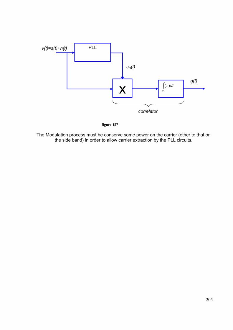
205
figure 157
The Modulation process must be conserve some power on the carrier (other to that on the side band) in order to allow carrier extraction by the PLL circuits.
PLL
x ∫T
dt(..)
v(t)=s(t)+n(t)
sR(t)
g(t)
correlator
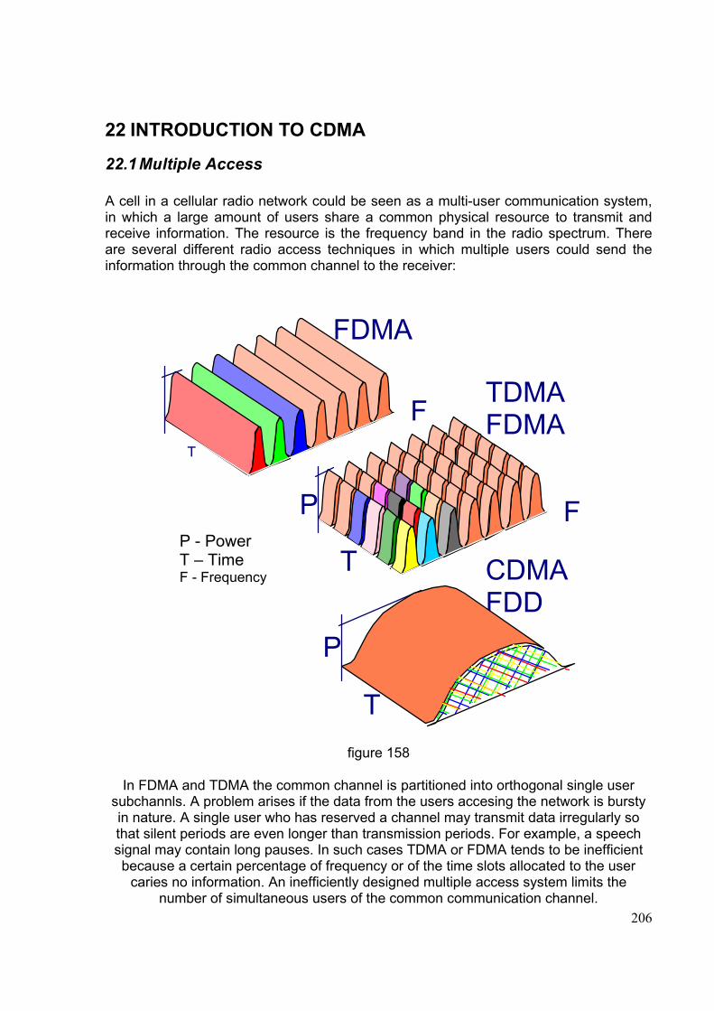
206
P - Power T – Time F - Frequency
T
P
T
F
P
T
FDMA
TDMA FDMA
CDMA FDD
F
22 INTRODUCTION TO CDMA
22.1 Multiple Access A cell in a cellular radio network could be seen as a multi-user communication system, in which a large amount of users share a common physical resource to transmit and receive information. The resource is the frequency band in the radio spectrum. There are several different radio access techniques in which multiple users could send the information through the common channel to the receiver:
figure 158
In FDMA and TDMA the common channel is partitioned into orthogonal single user subchannls. A problem arises if the data from the users accesing the network is bursty in nature. A single user who has reserved a channel may transmit data irregularly so that silent periods are even longer than transmission periods. For example, a speech signal may contain long pauses. In such cases TDMA or FDMA tends to be inefficient because a certain percentage of frequency or of the time slots allocated to the user
caries no information. An inefficiently designed multiple access system limits the number of simultaneous users of the common communication channel.
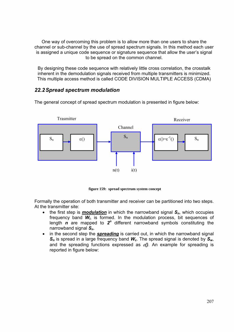
207
One way of overcoming this problem is to allow more than one users to share the channel or sub-channel by the use of spread spectrum signals. In this method each user is assigned a unique code sequence or signature sequence that allow the user’s signal
to be spread on the common channel.
By designing these code sequence with relatively little cross correlation, the crosstalk inherent in the demodulation signals received from multiple transmitters is minimized. This multiple access method is called CODE DIVISION MULTIPLE ACCESS (CDMA)
22.2 Spread spectrum modulation The general concept of spread spectrum modulation is presented in figure below:
figure 159: spread spectrum system concept
Formally the operation of both transmitter and receiver can be partitioned into two steps. At the transmitter site:
• the first step is modulation in which the narrowband signal Sn, which occupies frequency band Wi, is formed. In the modulation process, bit sequences of length n are mapped to 2n different narrowband symbols constituting the narrowband signal Sn.
• in the second step the spreading is carried out, in which the narrowband signal Sn is spread in a large frequency band Wc. The spread signal is denoted by Sw, and the spreading functions expressed as ε(). An example for spreading is reported in figure below:
Sn Sn ε() ε()=ε-1()
Sn
Trasmitter
Channel
Receiver
n(t) i(t)
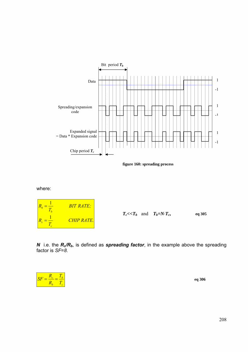
208
figure 160: spreading process
where:
RATE. CHIP
TR
RATE; BIT T
R
cc
bb
1
1
=
=
Tc<<Tb and Tb=N⋅Tc, eq 305
N i.e. the Rc/Rb, is defined as spreading factor, in the example above the spreading factor is SF=8.
c
b
b
c
TT
RRSF == eq 306
Data 1
-1
Spreading/expansion code
1
-1
Expanded signal = Data * Expansion code
1
-1
Chip period Tc
Bit period Tb
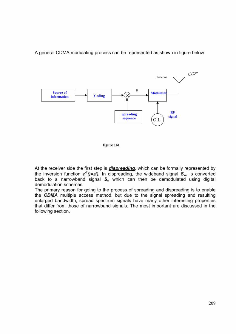
209
A general CDMA modulating process can be represented as shown in figure below:
figure 161
At the receiver side the first step is dispreading, which can be formally represented by the inversion function ε-1()=ε(). In dispreading, the wideband signal Sw, is converted back to a narrowband signal Sn which can then be demodulated using digital demodulation schemes. The primary reason for going to the process of spreading and dispreading is to enable the CDMA multiple access method, but due to the signal spreading and resulting enlarged bandwidth, spread spectrum signals have many other interesting properties that differ from those of narrowband signals. The most important are discussed in the following section.
Source of information Coding
Antenna
Spreading sequence O.L.
Modulator
RF signal
B
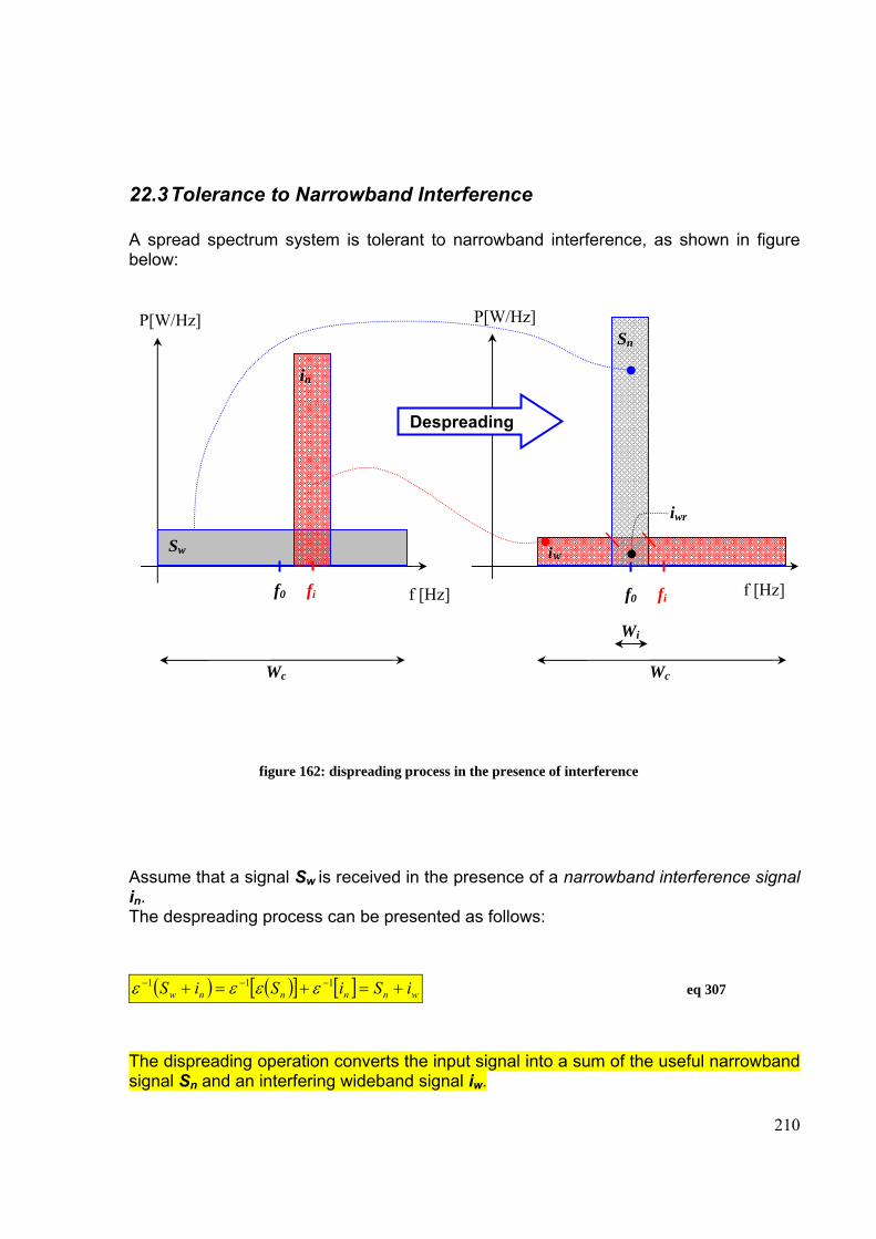
210
22.3 Tolerance to Narrowband Interference A spread spectrum system is tolerant to narrowband interference, as shown in figure below:
figure 162: dispreading process in the presence of interference
Assume that a signal Sw is received in the presence of a narrowband interference signal in. The despreading process can be presented as follows:
( ) ( )[ ] [ ] wnnnnw iSiSiS +=+=+ −−− 111 εεεε eq 307
The dispreading operation converts the input signal into a sum of the useful narrowband signal Sn and an interfering wideband signal iw.
Sw iW
in
Sn P[W/Hz]
f [Hz] f [Hz] f0 fi f0 fi
Wc Wc
Despreading
Wi
iwr
P[W/Hz]
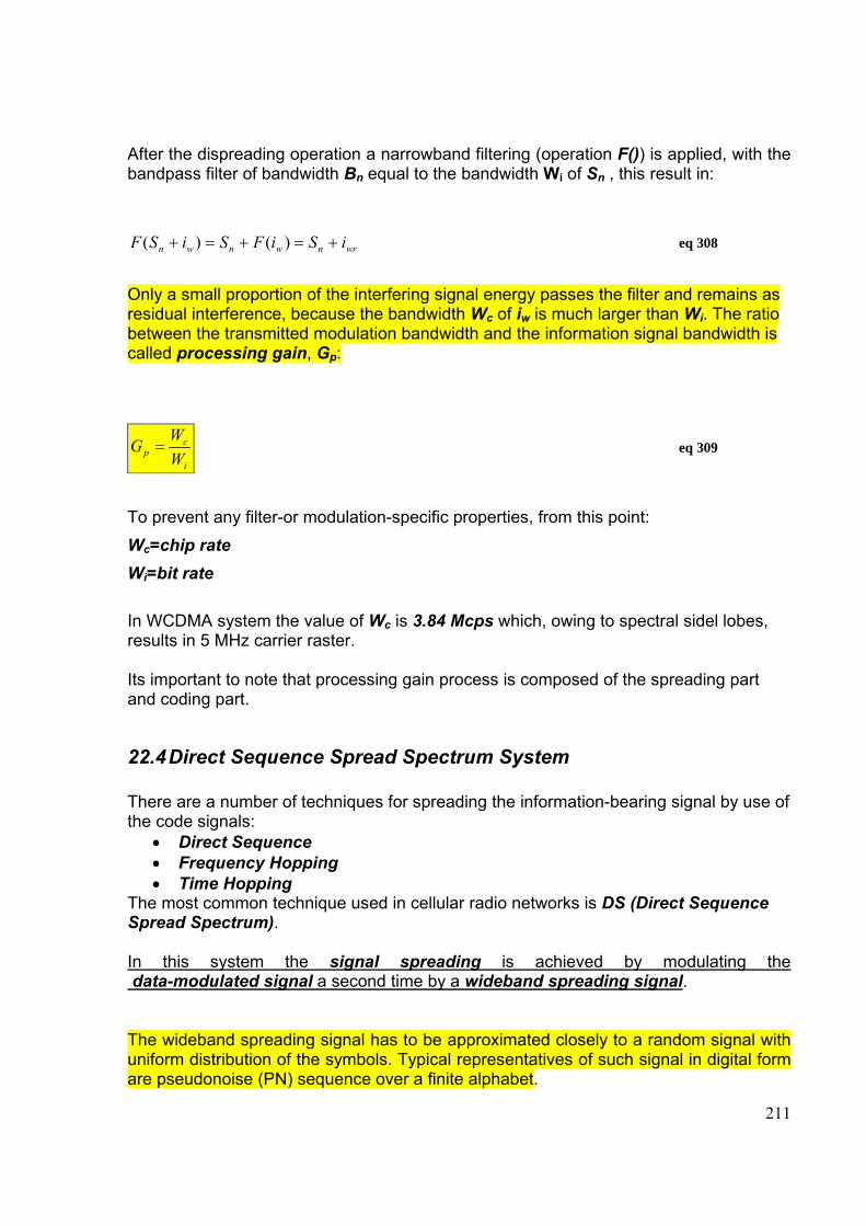
211
After the dispreading operation a narrowband filtering (operation F()) is applied, with the bandpass filter of bandwidth Bn equal to the bandwidth Wi of Sn , this result in:
wrnwnwn iSiFSiSF +=+=+ )()( eq 308
Only a small proportion of the interfering signal energy passes the filter and remains as residual interference, because the bandwidth Wc of iw is much larger than Wi. The ratio between the transmitted modulation bandwidth and the information signal bandwidth is called processing gain, Gp:
i
cp W
WG = eq 309
To prevent any filter-or modulation-specific properties, from this point: Wc=chip rate Wì=bit rate In WCDMA system the value of Wc is 3.84 Mcps which, owing to spectral sidel lobes, results in 5 MHz carrier raster. Its important to note that processing gain process is composed of the spreading part and coding part.
22.4 Direct Sequence Spread Spectrum System There are a number of techniques for spreading the information-bearing signal by use of the code signals:
• Direct Sequence • Frequency Hopping • Time Hopping
The most common technique used in cellular radio networks is DS (Direct Sequence Spread Spectrum). In this system the signal spreading is achieved by modulating the data-modulated signal a second time by a wideband spreading signal. The wideband spreading signal has to be approximated closely to a random signal with uniform distribution of the symbols. Typical representatives of such signal in digital form are pseudonoise (PN) sequence over a finite alphabet.
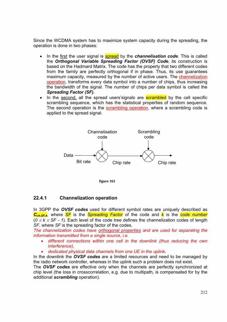
212
Since the WCDMA system has to maximize system capacity during the spreading, the operation is done in two phases:
• In the first the user signal is spread by the channelisation code. This is called the Orthogonal Variable Spreading Factor (OVSF) Code, its construction is based on the Hadmard Matrix. The code has the property that two different codes from the family are perfectly orthogonal if in phase. Thus, its use guarantees maximum capacity, measured by the number of active users. The channelization operation, transforms every data symbol into a number of chips, thus increasing the bandwidth of the signal. The number of chips per data symbol is called the Spreading Factor (SF).
• In the second, all the spread users’signals are scrambled by the cell specific scrambling sequence, which has the statistical properties of random sequence. The second operation is the scrambling operation, where a scrambling code is applied to the spread signal.
figure 163
22.4.1 Channelization operation
In 3GPP the OVSF codes used for different symbol rates are uniquely described as Cch,SF,k, where SF is the Spreading Factor of the code and k is the code number (0 ≤ k ≤ SF - 1). Each level of the code tree defines the channelization codes of length SF, where SF is the spreading factor of the codes. The channelization codes have orthogonal properties and are used for separating the information transmitted from a single source, i.e.
• different connections within one cell in the downlink (thus reducing the own interference),
• dedicated physical data channels from one UE in the uplink. In the downlink the OVSF codes are a limited resources and need to be managed by the radio network controller, whereas in the uplink such a problem does not exist. The OVSF codes are effective only when the channels are perfectly synchronized at chip level (the loss in crosscorrelation, e.g. due to multipath, is compensated for by the additional scrambling operation).
Data Bit rate Chip rate Chip rate
Channelisation code
Scrambling code
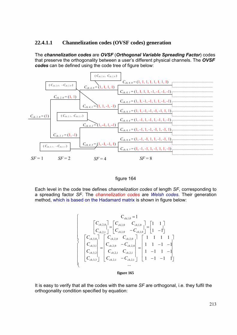
213
22.4.1.1 Channelization codes (OVSF codes) generation The channelization codes are OVSF (Orthogonal Variable Spreading Factor) codes that preserve the orthogonality between a user’s different physical channels. The OVSF codes can be defined using the code tree of figure below:
figure 164
Each level in the code tree defines channelization codes of length SF, corresponding to a spreading factor SF. The channelization codes are Welsh codes. Their generation method, which is based on the Hadamard matrix is shown in figure below:
⎪⎪⎪⎪⎪
⎩
⎪⎪⎪⎪⎪
⎨
⎧
⎥⎥⎥⎥
⎦
⎤
⎢⎢⎢⎢
⎣
⎡
−−−−−−
=
⎥⎥⎥⎥
⎦
⎤
⎢⎢⎢⎢
⎣
⎡
−
−=
⎥⎥⎥⎥
⎦
⎤
⎢⎢⎢⎢
⎣
⎡
⎥⎦
⎤⎢⎣
⎡−
=⎥⎦
⎤⎢⎣
⎡−
=⎥⎦
⎤⎢⎣
⎡=
...111111111111
111111
111C
1,2,1,2,
1,2,1,2,
0,2,0,2,
0,2,0,2,
3,3,
2,3,
1,3,
0,3,
0,1,
0,1,
0,1,
0,1,
1,2,
0,2,
ch,1,0
chch
chch
chch
chch
ch
ch
ch
ch
ch
ch
ch
ch
ch
ch
CCCCCC
CC
CCCC
CC
CC
CC
figure 165
It is easy to verify that all the codes with the same SF are orthogonal, i.e. they fulfil the orthogonality condition specified by equation:
Cch, 1, 0 = (1)
Cch, 2, 0 = (1, 1)
Cch, 2, 1 = (1, -1)
Cch, 4, 1 = (1, 1, -1, -1)
Cch, 4, 0 = (1, 1, 1, 1)
Cch, 4, 3 = (1, -1, -1, 1)
Cch, 4, 2 = (1, -1, 1, -1)
Cch, 8, 0 = (1, 1, 1, 1, 1, 1, 1, 1)
Cch, 8, 1 = (1, 1, 1, 1, -1, -1, -1, -1)
Cch, 8, 2 = (1, 1, -1, -1, 1, 1, -1, -1)
Cch, 8, 3 = (1, 1, -1, -1, -1, -1, 1, 1)
Cch, 8, 4 = (1, -1, 1, -1, 1, -1, 1, -1)
Cch, 8, 5 = (1, -1, 1, -1, -1, 1, -1, 1)
Cch, 8, 6 = (1, -1, -1, 1, 1, -1, -1, 1)
Cch, 8, 7 = (1, -1, -1, 1, -1, 1, 1, -1)
SF = 8SF = 4SF = 2SF = 1
( Cch, 2, 0 , Cch, 2, 0 )
( Cch, 2, 0 , - Cch, 2, 0 )
( Cch, 2, 1 , - Cch, 2, 1 )
( Cch, 2, 1 , Cch, 2, 1 )
214
01
0,2,1 =⋅∑
−
=
SF
kkk SS eq 310
This orthogonality, however, is not guaranteed between a generic code and the codes belonging to its subtree. As a consequence, the selection of one code, blocks the corresponding subtree.
22.4.2 Scrambling operation The second operation is the scrambling operation, where a scrambling code is applied on top of the spread signal, so it does not change the signal bandwidth but only makes the signals from different sources separable from each other. With the scrambling, it would not matter if the actual spreading were performed with identical codes for several transmitters. With the scrambling operation the real (I) part imaginary (Q) parts of the spread signal are further multiplied by a complex-valued scrambling code. The scrambling codes are used to
• separate different cells in the downlink, • separate different terminals in the uplink.
The scrambling codes have good correlation properties (interference averaging) and are always used on top of spreading codes, thus not affecting the transmission bandwidth.
22.5 Orthogonal sequences reminder
Let us consider two finit energy signals ( )ts1 and ( )ts2 defined in the interval [a, b]. The AUTOCORRELATION ( )τiiR of the finite energy signal ( )tsi (i = 1, 2) is defined as
( ) ( ) ( ) dttstsR i
b
aiii
∗∫ += ττ ˆ eq 311
The CROSS CORRELATIONS ( )τ21R and ( )τ12R between the finite energy signals ( )ts1 and ( )ts2 are defined as
( ) ( ) ( ) dttstsRb
a
∗∫ += 2121 ˆ ττ eq 312
and
( ) ( ) ( ) dttstsRb
a
∗∫ += 1212 ˆ ττ eq 313
215
Definition:
The finite energy signals ( )ts1 and ( )ts2 are ORTHOGONAL ⇔ ( ) 0021 =R ⇔ ( ) 0012 =R .
In other words, the finite energy signals ( )ts1 and ( )ts2 are ORTHOGONAL ⇔
( ) ( ) 021 =∗∫ dttstsb
a
⇔ ( ) ( ) 012 =∗∫ dttstsb
a
eq 314
Let us now suppose that ( )ts1 and ( )ts2 are two channelisation sequences with the same SF, as shown in figure below. We will show that
the sequences ( )ts1 and ( )ts2 are ORTHOGONAL ⇔ 01
0,2,1 =⋅∑
−
=
SF
kkk SS
Note:
The term ∑−
=
⋅1
0,2,1
SF
kkk SS is also called the cross-product between the two
sequences. If we indicate
[ ][ ]1,22,21,22
1,12,11,11
,,ˆ
,,ˆ
−
−
=
=
SF
SF
SSSS
SSSS
L
L eq 315
the cross-product between the two sequences can also be indicated as
TSS 21 ⋅ eq 316
Proof:
The sequences ( )ts1 and ( )ts2 are ORTHOGONAL ⇔ ( ) ( ) 021 =∗∫ dttstsbT
⇔
⇔ 01
0,2,1 =⋅⋅∑
−
=
SF
kckk TSS ⇔ 0
1
0,2,1 =⋅∑
−
=
SF
kkk SS eq 317
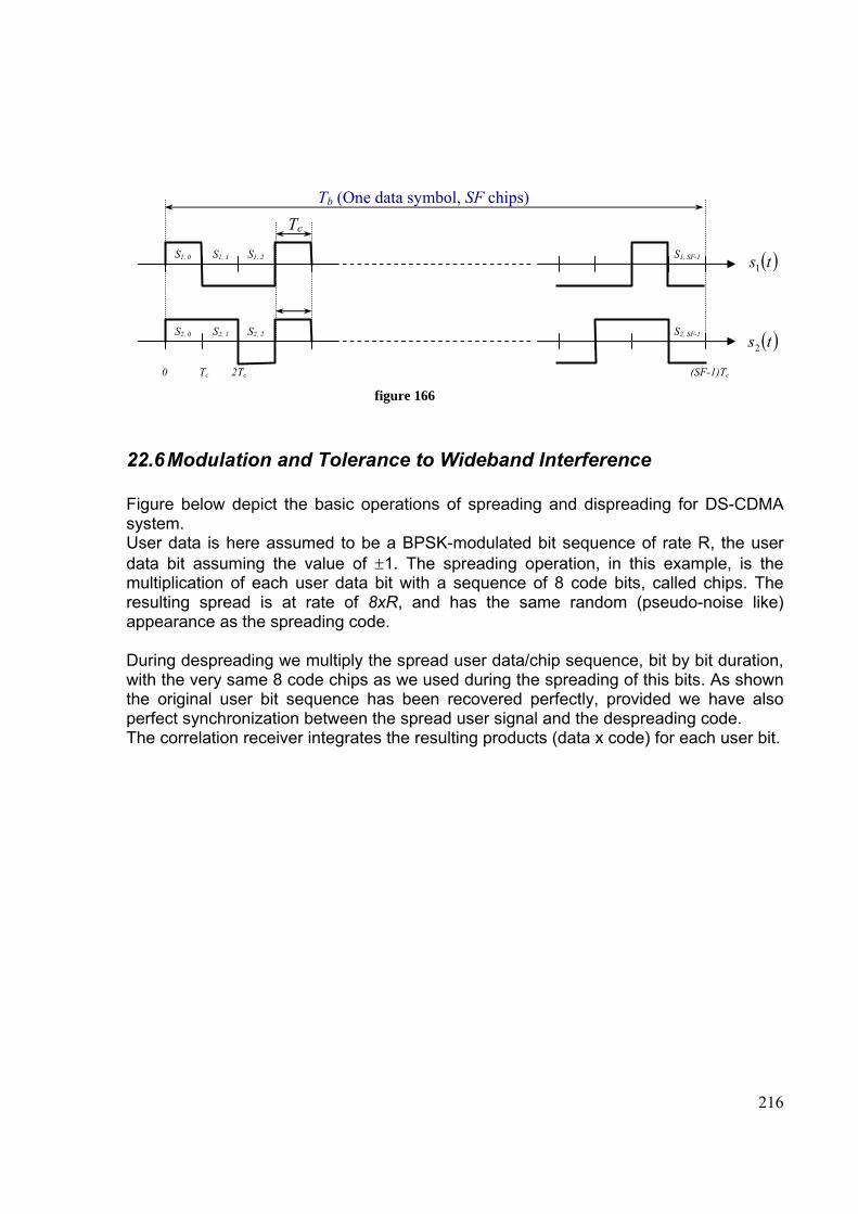
216
figure 166
22.6 Modulation and Tolerance to Wideband Interference Figure below depict the basic operations of spreading and dispreading for DS-CDMA system. User data is here assumed to be a BPSK-modulated bit sequence of rate R, the user data bit assuming the value of ±1. The spreading operation, in this example, is the multiplication of each user data bit with a sequence of 8 code bits, called chips. The resulting spread is at rate of 8xR, and has the same random (pseudo-noise like) appearance as the spreading code. During despreading we multiply the spread user data/chip sequence, bit by bit duration, with the very same 8 code chips as we used during the spreading of this bits. As shown the original user bit sequence has been recovered perfectly, provided we have also perfect synchronization between the spread user signal and the despreading code. The correlation receiver integrates the resulting products (data x code) for each user bit.
Tc
Tb (One data symbol, SF chips)
Tc 2Tc 0 (SF-1)Tc
( )ts1
( )ts2
S1, 0 S1, 1 S1, 2 S1, SF-1
S2, 0 S2, 1 S2, 2 S2, SF-1
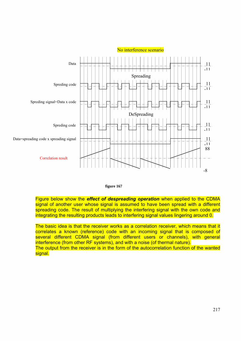
217
figure 167
Figure below show the effect of despreading operation when applied to the CDMA signal of another user whose signal is assumed to have been spread with a different spreading code. The result of multiplying the interfering signal with the own code and integrating the resulting products leads to interfering signal values lingering around 0. The basic idea is that the receiver works as a correlation receiver, which means that it correlates a known (reference) code with an incoming signal that is composed of several different CDMA signal (from different users or channels), with general interference (from other RF systems), and with a noise (of thermal nature). The output from the receiver is in the form of the autocorrelation function of the wanted signal.
Spreding signal=Data x code 11-11
Spreding code 11-11
Data 11-11
Correlation result
88
-8
Spreading
DeSpreading
Spreding code 11-11
Data=spreading code x spreading signal
11-11
No interference scenario
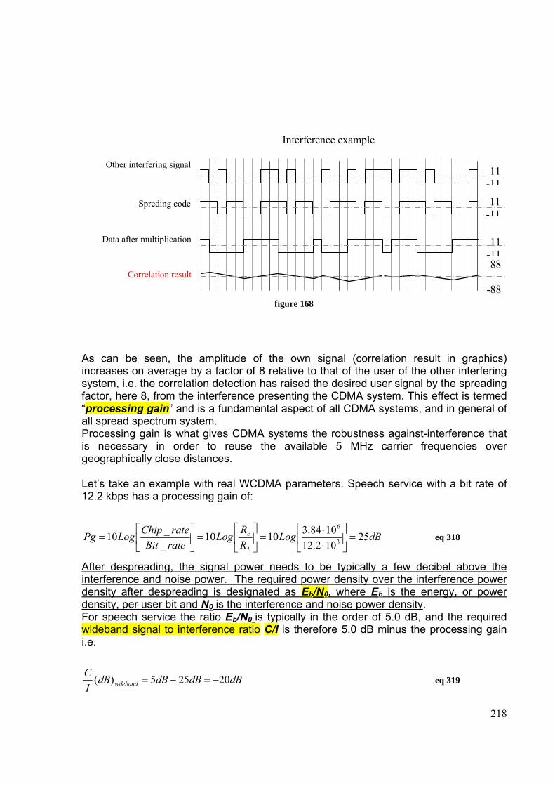
218
figure 168
As can be seen, the amplitude of the own signal (correlation result in graphics) increases on average by a factor of 8 relative to that of the user of the other interfering system, i.e. the correlation detection has raised the desired user signal by the spreading factor, here 8, from the interference presenting the CDMA system. This effect is termed “processing gain” and is a fundamental aspect of all CDMA systems, and in general of all spread spectrum system. Processing gain is what gives CDMA systems the robustness against-interference that is necessary in order to reuse the available 5 MHz carrier frequencies over geographically close distances. Let’s take an example with real WCDMA parameters. Speech service with a bit rate of 12.2 kbps has a processing gain of:
dBLogRRLog
rateBitrateChipLogPg
b
c 25102.121084.31010
__10 3
6
=⎥⎦
⎤⎢⎣
⎡⋅⋅
=⎥⎦
⎤⎢⎣
⎡=⎥
⎦
⎤⎢⎣
⎡= eq 318
After despreading, the signal power needs to be typically a few decibel above the interference and noise power. The required power density over the interference power density after despreading is designated as Eb/N0, where Eb is the energy, or power density, per user bit and N0 is the interference and noise power density. For speech service the ratio Eb/N0 is typically in the order of 5.0 dB, and the required wideband signal to interference ratio C/I is therefore 5.0 dB minus the processing gain i.e.
dBdBdBdBIC
wdeband 20255)( −=−= eq 319
Spreding code 11-11
Other interfering signal 11-11
Data after multiplication 11-11
Correlation result 88
-88
Interference example
219
In other words, the signal power can be 20 dB under the interference or thermal noise power, and the WCDMA receiver can still detect the signal. Due to spreading and despreading, C/I can be lower in WCDMA than, for example, in GSM. A good quality speech connection in GSM requires C/I=9-10 dB. Since the wideband signal can be around the thermal noise level, its detection is difficult without knowledge of the spreading sequence. For this reason spread spectrum systems were originated in military applications where the wideband nature of the signal allowed have to be hidden below omnipresent thermal noise. It should be observed that the more is the bit rate Rb, the lower is Pg(dB), therefore higher bit-rate service require an increasing C/I.
Rb (Kbit/sec) Pg Pg(dB)
12.2 314.7541 25.0 64 60 17.8 384 10 10.0 2000 1.92 2.8
table 8
It should be also observed that the processing gain comes at the price of an increased transmission bandwidth (by the amount of the processing gain).
22.7 Uplink Modulation In the uplink direction there are basically two additional terminal-oriented criteria that need to be taken into account in the definition of the modulation and spreading methods. The uplink modulation should be designed so that the terminal amplifier efficiency is maximized and/or the audible interference from the terminal is minimized. Discontinuosus uplink transmission can cause audible interference to audio equipment that is very close to the terminal; this is a completely separate issue from the interference in the air interface. With GSM operation we are familiar with the occasional audible interference with audio equipment that is not properly protected. The interference from GSM has a frequency of 217 Hz, which is determined, by the GSM frame frequency. With WCDMA system, the same issues arise when discontinuous uplink transmission is used, for example with a speech service. During the silent period no information bits need to be transmitted, only the information for link maintenance purposes, such as power control with a 1.5 KHz command rate. With such a rate the transmission of the pilot and the power control symbols with time multiplexing in the uplink direction would cause audible interference in the middle of the telephony voice
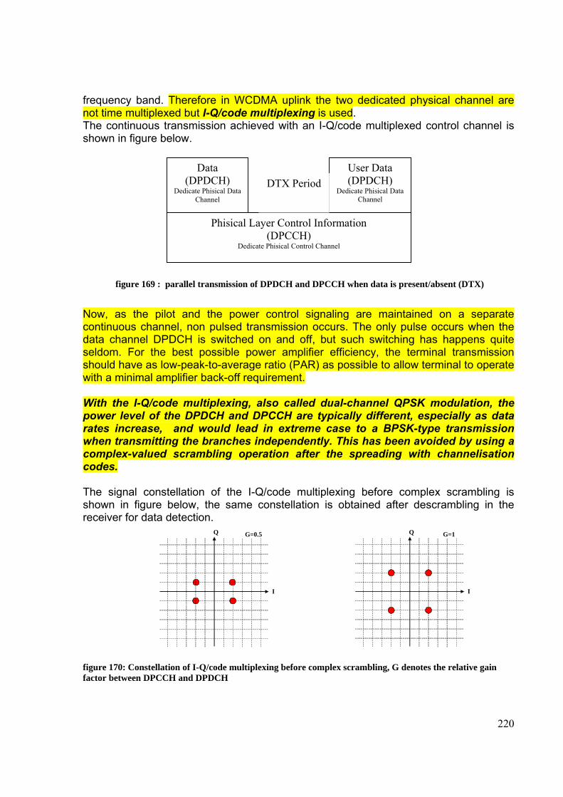
220
frequency band. Therefore in WCDMA uplink the two dedicated physical channel are not time multiplexed but I-Q/code multiplexing is used. The continuous transmission achieved with an I-Q/code multiplexed control channel is shown in figure below.
figure 169 : parallel transmission of DPDCH and DPCCH when data is present/absent (DTX)
Now, as the pilot and the power control signaling are maintained on a separate continuous channel, non pulsed transmission occurs. The only pulse occurs when the data channel DPDCH is switched on and off, but such switching has happens quite seldom. For the best possible power amplifier efficiency, the terminal transmission should have as low-peak-to-average ratio (PAR) as possible to allow terminal to operate with a minimal amplifier back-off requirement. With the I-Q/code multiplexing, also called dual-channel QPSK modulation, the power level of the DPDCH and DPCCH are typically different, especially as data rates increase, and would lead in extreme case to a BPSK-type transmission when transmitting the branches independently. This has been avoided by using a complex-valued scrambling operation after the spreading with channelisation codes. The signal constellation of the I-Q/code multiplexing before complex scrambling is shown in figure below, the same constellation is obtained after descrambling in the receiver for data detection.
G=0.5
I
Q
I
Q G=1
figure 170: Constellation of I-Q/code multiplexing before complex scrambling, G denotes the relative gain factor between DPCCH and DPDCH
Data (DPDCH)
Dedicate Phisical Data Channel
User Data (DPDCH)
Dedicate Phisical Data Channel
Phisical Layer Control Information (DPCCH)
Dedicate Phisical Control Channel
DTX Period
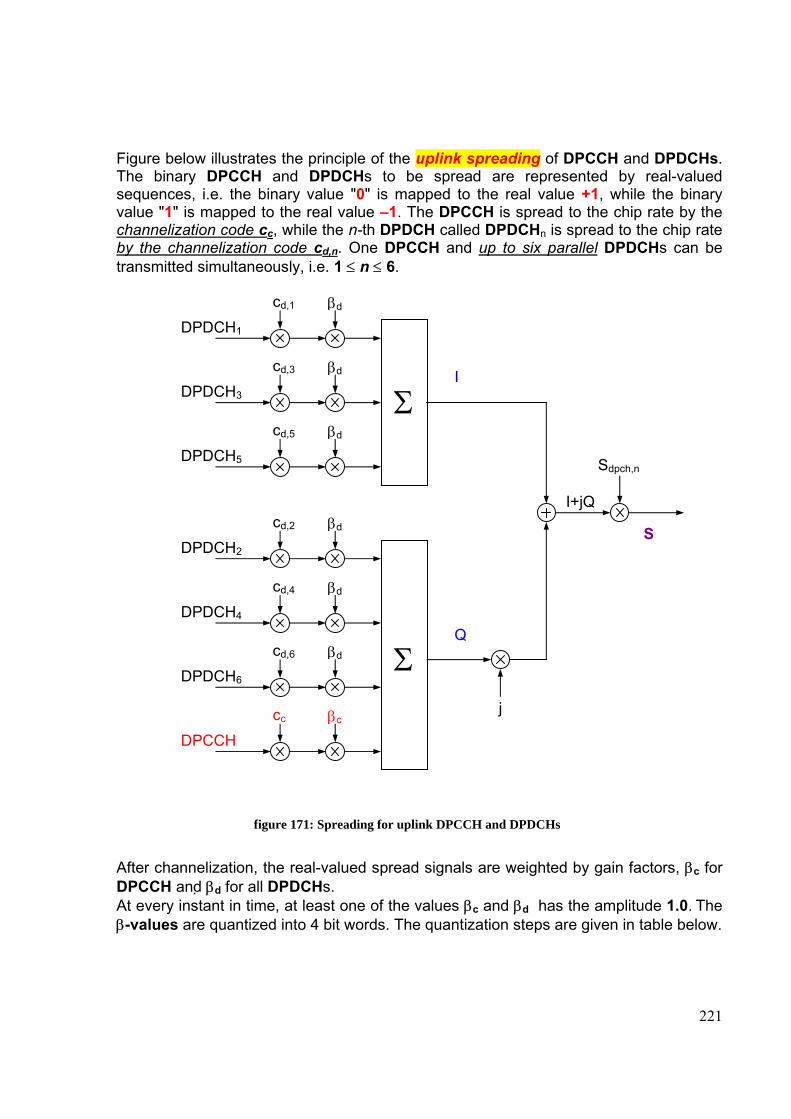
221
Figure below illustrates the principle of the uplink spreading of DPCCH and DPDCHs. The binary DPCCH and DPDCHs to be spread are represented by real-valued sequences, i.e. the binary value "0" is mapped to the real value +1, while the binary value "1" is mapped to the real value –1. The DPCCH is spread to the chip rate by the channelization code cc, while the n-th DPDCH called DPDCHn is spread to the chip rate by the channelization code cd,n. One DPCCH and up to six parallel DPDCHs can be transmitted simultaneously, i.e. 1 ≤ n ≤ 6.
figure 171: Spreading for uplink DPCCH and DPDCHs
After channelization, the real-valued spread signals are weighted by gain factors, βc for DPCCH and βd for all DPDCHs. At every instant in time, at least one of the values βc and βd has the amplitude 1.0. The β-values are quantized into 4 bit words. The quantization steps are given in table below.
I
Σ
j
cd,1 βd
Sdpch,n
I+jQ
DPDCH1
Q
cd,3 βd
DPDCH3
cd,5 βd
DPDCH5
cd,2 βd
DPDCH2
cd,4 βd
DPDCH4
cd,6 βd
DPDCH6
cc βc
DPCCH
Σ
S
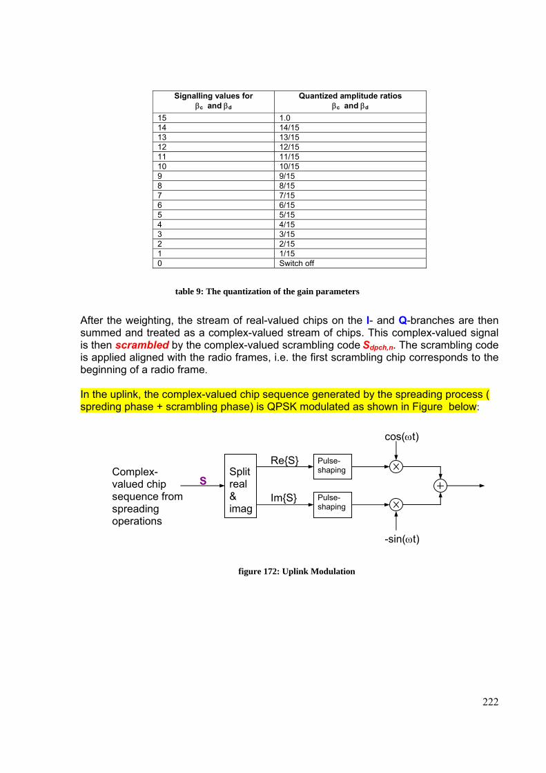
222
Signalling values for βc and βd
Quantized amplitude ratios βc and βd
15 1.0 14 14/15 13 13/15 12 12/15 11 11/15 10 10/15 9 9/15 8 8/15 7 7/15 6 6/15 5 5/15 4 4/15 3 3/15 2 2/15 1 1/15 0 Switch off
table 9: The quantization of the gain parameters
After the weighting, the stream of real-valued chips on the I- and Q-branches are then summed and treated as a complex-valued stream of chips. This complex-valued signal is then scrambled by the complex-valued scrambling code Sdpch,n. The scrambling code is applied aligned with the radio frames, i.e. the first scrambling chip corresponds to the beginning of a radio frame. In the uplink, the complex-valued chip sequence generated by the spreading process ( spreding phase + scrambling phase) is QPSK modulated as shown in Figure below:
figure 172: Uplink Modulation
S Im{S}
Re{S}
cos(ωt)
Complex-valued chip sequence from spreading operations
-sin(ωt)
Split real & imag
Pulse- shaping
Pulse- shaping
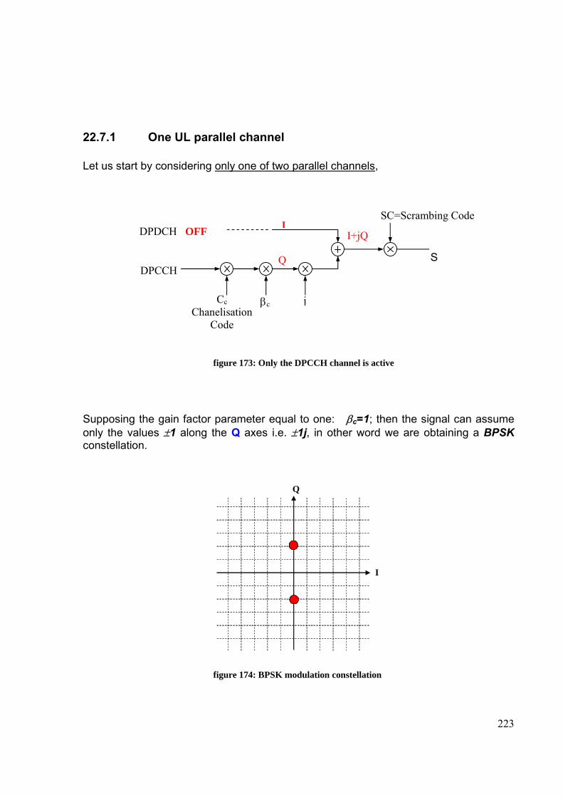
223
22.7.1 One UL parallel channel Let us start by considering only one of two parallel channels,
figure 173: Only the DPCCH channel is active
Supposing the gain factor parameter equal to one: βc=1; then the signal can assume only the values ±1 along the Q axes i.e. ±1j, in other word we are obtaining a BPSK constellation.
I
Q
figure 174: BPSK modulation constellation
jβc Cc Chanelisation
Code
SC=Scrambing Code
I+jQ
DPCCH
DPDCH OFF
Q
I
S
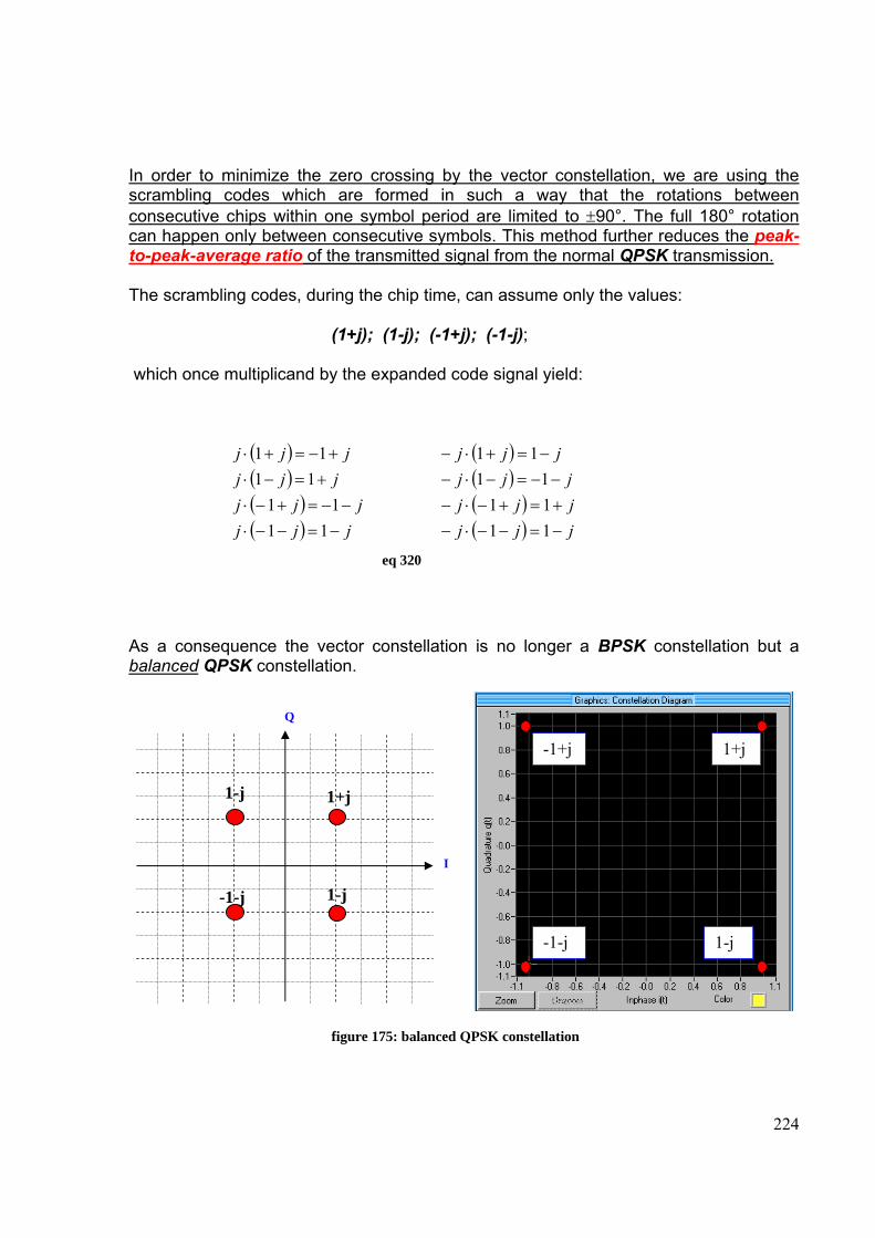
224
In order to minimize the zero crossing by the vector constellation, we are using the scrambling codes which are formed in such a way that the rotations between consecutive chips within one symbol period are limited to ±90°. The full 180° rotation can happen only between consecutive symbols. This method further reduces the peak-to-peak-average ratio of the transmitted signal from the normal QPSK transmission. The scrambling codes, during the chip time, can assume only the values:
(1+j); (1-j); (-1+j); (-1-j); which once multiplicand by the expanded code signal yield:
( )( )( )( ) jjj
jjjjjj
jjj
−=−−⋅−−=+−⋅
+=−⋅+−=+⋅
1111
1111
( )( )( )( ) jjj
jjjjjj
jjj
−=−−⋅−+=+−⋅−−−=−⋅−
−=+⋅−
111111
11
eq 320
As a consequence the vector constellation is no longer a BPSK constellation but a balanced QPSK constellation.
figure 175: balanced QPSK constellation
I
Q
1-j -1-j
1+j 1-j
1+j
1-j
-1+j
-1-j
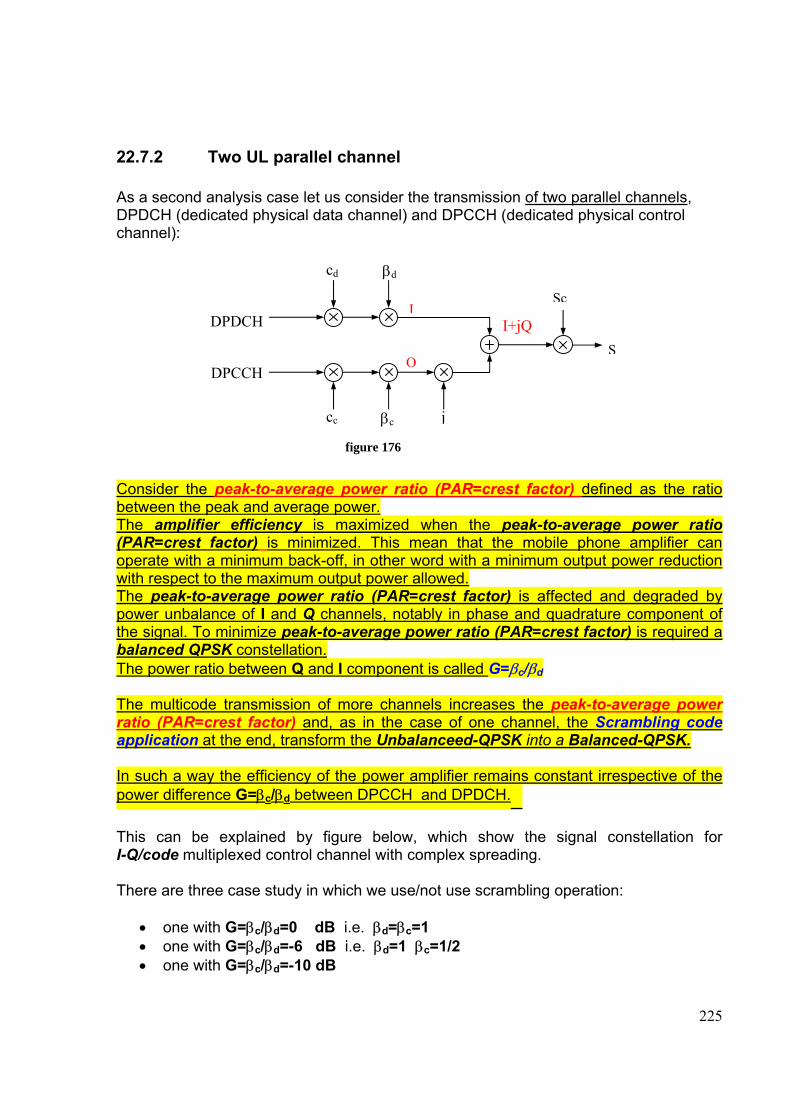
225
22.7.2 Two UL parallel channel As a second analysis case let us consider the transmission of two parallel channels, DPDCH (dedicated physical data channel) and DPCCH (dedicated physical control channel):
figure 176
Consider the peak-to-average power ratio (PAR=crest factor) defined as the ratio between the peak and average power. The amplifier efficiency is maximized when the peak-to-average power ratio (PAR=crest factor) is minimized. This mean that the mobile phone amplifier can operate with a minimum back-off, in other word with a minimum output power reduction with respect to the maximum output power allowed. The peak-to-average power ratio (PAR=crest factor) is affected and degraded by power unbalance of I and Q channels, notably in phase and quadrature component of the signal. To minimize peak-to-average power ratio (PAR=crest factor) is required a balanced QPSK constellation. The power ratio between Q and I component is called G=βc/βd The multicode transmission of more channels increases the peak-to-average power ratio (PAR=crest factor) and, as in the case of one channel, the Scrambling code application at the end, transform the Unbalanceed-QPSK into a Balanced-QPSK. In such a way the efficiency of the power amplifier remains constant irrespective of the power difference G=βc/βd between DPCCH and DPDCH. This can be explained by figure below, which show the signal constellation for I-Q/code multiplexed control channel with complex spreading. There are three case study in which we use/not use scrambling operation:
• one with G=βc/βd=0 dB i.e. βd=βc=1 • one with G=βc/βd=-6 dB i.e. βd=1 βc=1/2 • one with G=βc/βd=-10 dB
jβc cc
cd βd
I+jQ
DPCCH
DPDCH
Q
ISc
S
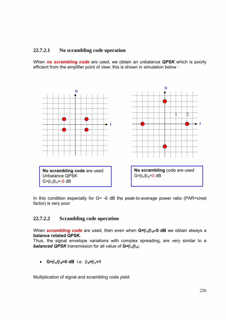
226
22.7.2.1 No scrambling code operation When no scrambling code are used, we obtain an unbalance QPSK which is poorly efficient from the amplifier point of view; this is shown in simulation below :
In this condition especially for G= -6 dB the peak-to-average power ratio (PAR=crest factor) is very poor
22.7.2.2 Scrambling code operation When scrambling code are used, then even when G=βc/βd≠0 dB we obtain always a balance rotated QPSK. Thus, the signal envelope variations with complex spreading, are very similar to a balanced QPSK transmission for all value of G=βc/βd:
• G=βc/βd=0 dB i.e. βd=βc=1 Multiplication of signal and scrambling code yield:
No scrambling code are used Unbalance QPSK G=βc/βd=-6 dB
No scrambling code are used G=βc/βd=0 dB
I
Q
1 2
I
Q
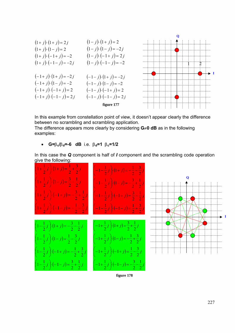
227
( ) ( )( ) ( )( ) ( )( ) ( ) jjj
jjjj
jjj
211211
211211
−=−−⋅+−=+−⋅+
=−⋅+=+⋅+
( ) ( )( ) ( )( ) ( )( ) ( ) 211
211211
211
−=−−⋅−=+−⋅−−=−⋅−
=+⋅−
jjjjjjjj
jj
( ) ( )( ) ( )( ) ( )( ) ( ) jjj
jjjj
jjj
211211211211
=−−⋅+−=+−⋅+−−=−⋅+−−=+⋅+−
( ) ( )( ) ( )( ) ( )( ) ( ) jjj
jjjj
jjj
211211211211
=−−⋅−−=+−⋅−−−=−⋅−−−=+⋅−−
figure 177
In this example from constellation point of view, it doesn’t appear clearly the difference between no scrambling and scrambling application. The difference appears more clearly by considering G≠0 dB as in the following examples:
• G=βc/βd=-6 dB i.e. βd=1 βc=1/2 In this case the Q component is half of I component and the scrambling code operation give the following:
( )
( )
( )
( ) jjj
jjj
jjj
jjj
23
211
211
21
231
211
21
231
211
23
211
211
−−=−−⋅⎟⎠⎞
⎜⎝⎛ +
+−=+−⋅⎟⎠⎞
⎜⎝⎛ +
−=−⋅⎟⎠⎞
⎜⎝⎛ +
+=+⋅⎟⎠⎞
⎜⎝⎛ +
( )
( )
( )
( ) jjj
jjj
jjj
jjj
23
211
211
21
231
211
21
231
211
23
211
211
+=−−⋅⎟⎠⎞
⎜⎝⎛ −−
−=+−⋅⎟⎠⎞
⎜⎝⎛ −−
+−=−⋅⎟⎠⎞
⎜⎝⎛ −−
−−=+⋅⎟⎠⎞
⎜⎝⎛ −−
( )
( )
( )
( ) jjj
jjj
jjj
jjj
21
231
211
23
211
211
23
211
211
21
231
211
+=−−⋅⎟⎠⎞
⎜⎝⎛ −
+−=+−⋅⎟⎠⎞
⎜⎝⎛ −
−=−⋅⎟⎠⎞
⎜⎝⎛ −
−−=+⋅⎟⎠⎞
⎜⎝⎛ −
( )
( )
( )
( ) jjj
jjj
jjj
jjj
21
231
211
23
211
211
23
211
211
21
231
211
−−=−−⋅⎟⎠⎞
⎜⎝⎛ +−
−=+−⋅⎟⎠⎞
⎜⎝⎛ +−
+−=−⋅⎟⎠⎞
⎜⎝⎛ +−
+=+⋅⎟⎠⎞
⎜⎝⎛ +−
figure 178
I
Q
1 2
I
Q
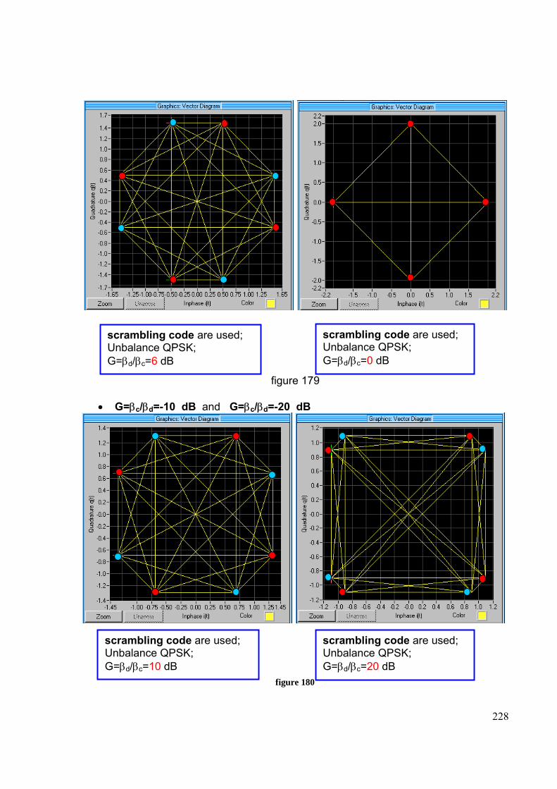
228
figure 179
• G=βc/βd=-10 dB and G=βc/βd=-20 dB
figure 180
scrambling code are used; Unbalance QPSK; G=βd/βc=6 dB
scrambling code are used; Unbalance QPSK; G=βd/βc=0 dB
scrambling code are used; Unbalance QPSK; G=βd/βc=10 dB
scrambling code are used; Unbalance QPSK; G=βd/βc=20 dB
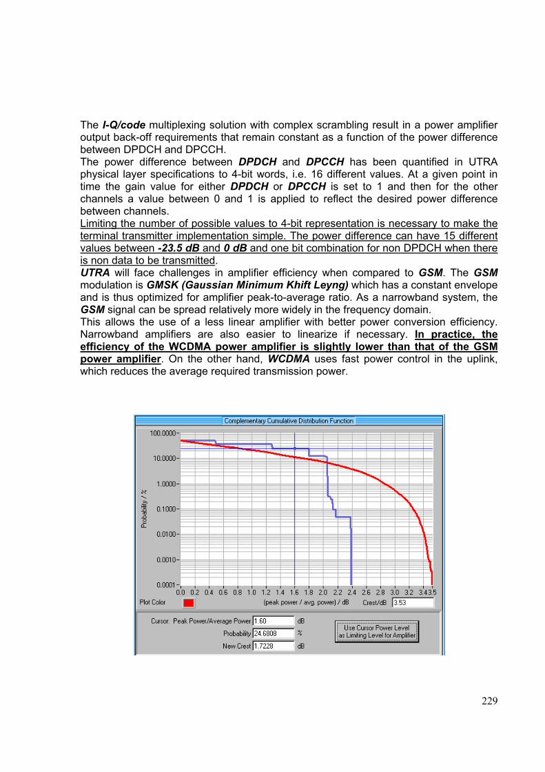
229
The I-Q/code multiplexing solution with complex scrambling result in a power amplifier output back-off requirements that remain constant as a function of the power difference between DPDCH and DPCCH. The power difference between DPDCH and DPCCH has been quantified in UTRA physical layer specifications to 4-bit words, i.e. 16 different values. At a given point in time the gain value for either DPDCH or DPCCH is set to 1 and then for the other channels a value between 0 and 1 is applied to reflect the desired power difference between channels. Limiting the number of possible values to 4-bit representation is necessary to make the terminal transmitter implementation simple. The power difference can have 15 different values between -23.5 dB and 0 dB and one bit combination for non DPDCH when there is non data to be transmitted. UTRA will face challenges in amplifier efficiency when compared to GSM. The GSM modulation is GMSK (Gaussian Minimum Khift Leyng) which has a constant envelope and is thus optimized for amplifier peak-to-average ratio. As a narrowband system, the GSM signal can be spread relatively more widely in the frequency domain. This allows the use of a less linear amplifier with better power conversion efficiency. Narrowband amplifiers are also easier to linearize if necessary. In practice, the efficiency of the WCDMA power amplifier is slightly lower than that of the GSM power amplifier. On the other hand, WCDMA uses fast power control in the uplink, which reduces the average required transmission power.
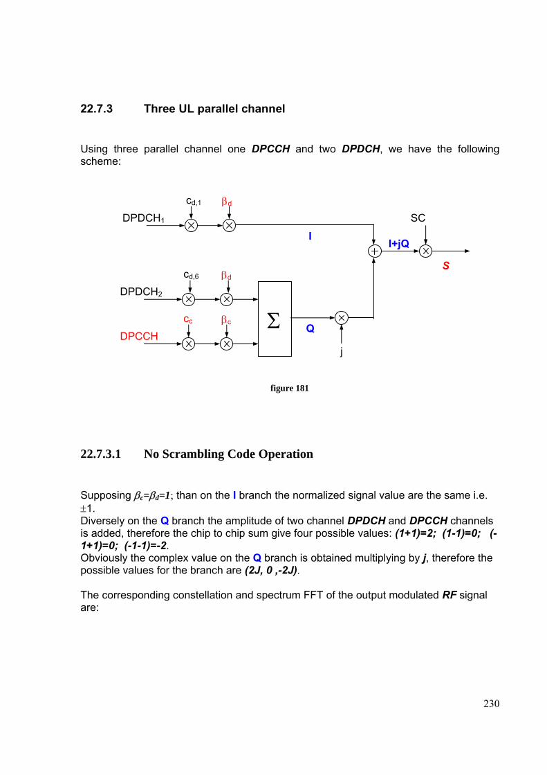
230
22.7.3 Three UL parallel channel Using three parallel channel one DPCCH and two DPDCH, we have the following scheme:
figure 181
22.7.3.1 No Scrambling Code Operation Supposing βc=βd=1; than on the I branch the normalized signal value are the same i.e. ±1. Diversely on the Q branch the amplitude of two channel DPDCH and DPCCH channels is added, therefore the chip to chip sum give four possible values: (1+1)=2; (1-1)=0; (-1+1)=0; (-1-1)=-2. Obviously the complex value on the Q branch is obtained multiplying by j, therefore the possible values for the branch are (2J, 0 ,-2J). The corresponding constellation and spectrum FFT of the output modulated RF signal are:
j
Q
cd,6 βd
DPDCH2
cc βc
DPCCH
Σ
SC
I+jQ
S
βdcd,1
DPDCH1
I
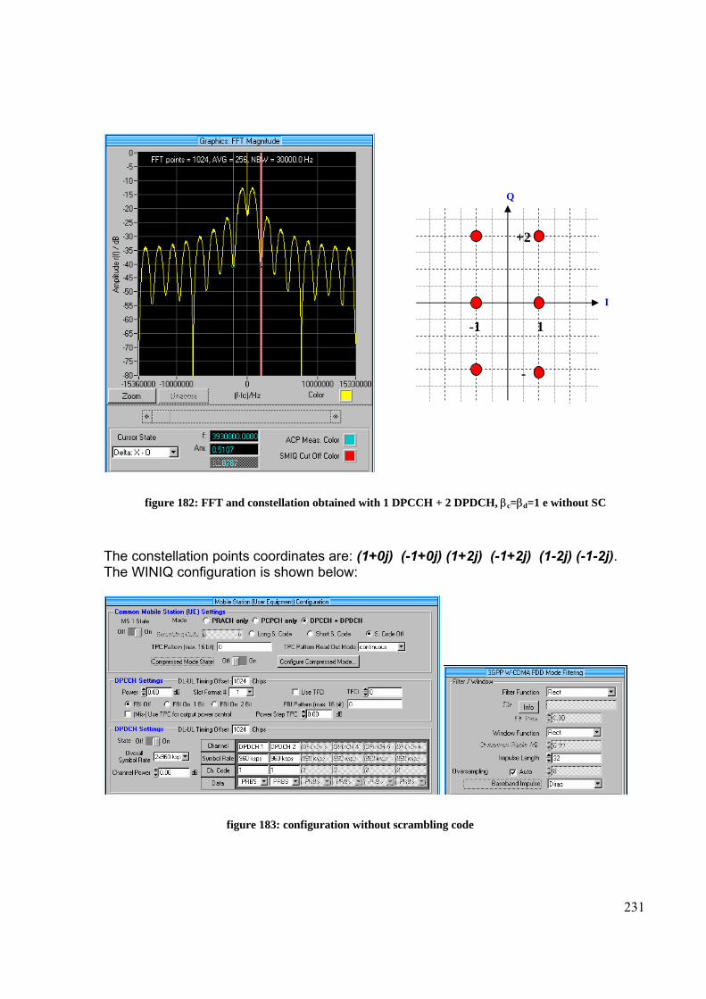
231
figure 182: FFT and constellation obtained with 1 DPCCH + 2 DPDCH, βc=βd=1 e without SC
The constellation points coordinates are: (1+0j) (-1+0j) (1+2j) (-1+2j) (1-2j) (-1-2j). The WINIQ configuration is shown below:
figure 183: configuration without scrambling code
I
Q
1 -1
+2j
-2j
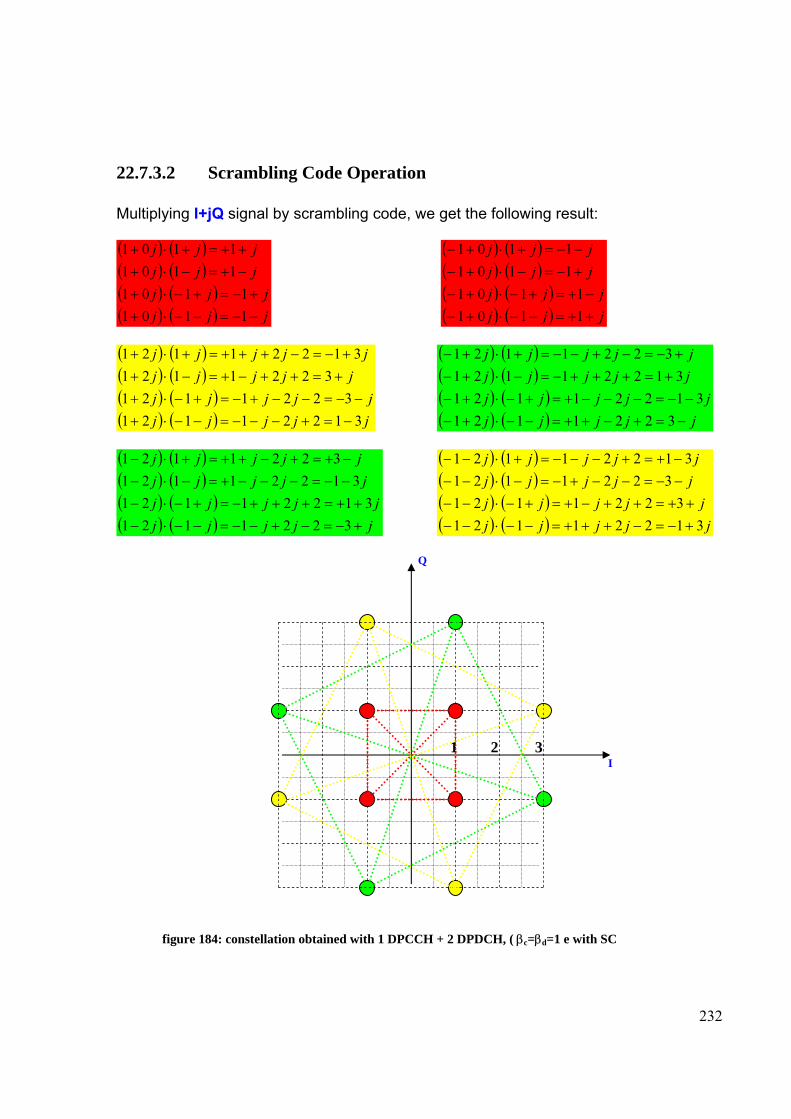
232
22.7.3.2 Scrambling Code Operation Multiplying I+jQ signal by scrambling code, we get the following result: ( ) ( )( ) ( )( ) ( )( ) ( ) jjj
jjjjjjjjj
−−=−−⋅++−=+−⋅+
−+=−⋅+++=+⋅+
11011101
11011101
( ) ( )( ) ( )( ) ( )( ) ( ) jjj
jjjjjjjjj
++=−−⋅+−−+=+−⋅+−
+−=−⋅+−−−=+⋅+−
11011101
11011101
( ) ( )( ) ( )( ) ( )( ) ( ) jjjjj
jjjjjjjjjj
jjjjj
312211213221121
322112131221121
−=+−−−=−−⋅+−−=−−+−=+−⋅+
+=++−+=−⋅++−=−+++=+⋅+
( ) ( )( ) ( )( ) ( )( ) ( ) jjjjj
jjjjjjjjjjjjjjj
−=+−++=−−⋅+−−−=−−−+=+−⋅+−
+=+++−=−⋅+−+−=−+−−=+⋅+−
322112131221121
312211213221121
( ) ( )( ) ( )( ) ( )( ) ( ) jjjjj
jjjjjjjjjj
jjjjj
+−=−+−−=−−⋅−++=+++−=+−⋅−
−−=−−−+=−⋅−−+=+−++=+⋅−
322112131221121
312211213221121
( ) ( )( ) ( )( ) ( )( ) ( ) jjjjj
jjjjjjjjjjjjjjj
312211213221121
322112131221121
+−=−+++=−−⋅−−++=++−+=+−⋅−−
−−=−−+−=−⋅−−−+=+−−−=+⋅−−
figure 184: constellation obtained with 1 DPCCH + 2 DPDCH, ( βc=βd=1 e with SC
I
Q
1 2 3
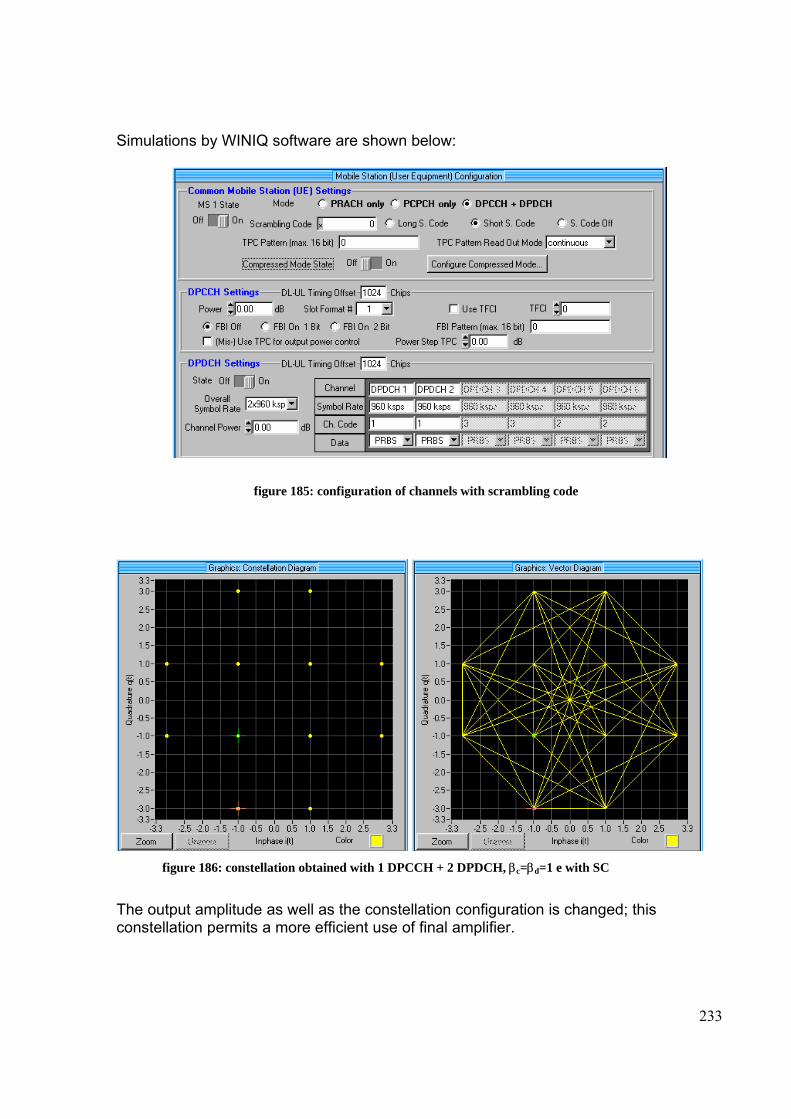
233
Simulations by WINIQ software are shown below:
figure 185: configuration of channels with scrambling code
figure 186: constellation obtained with 1 DPCCH + 2 DPDCH, βc=βd=1 e with SC
The output amplitude as well as the constellation configuration is changed; this constellation permits a more efficient use of final amplifier.
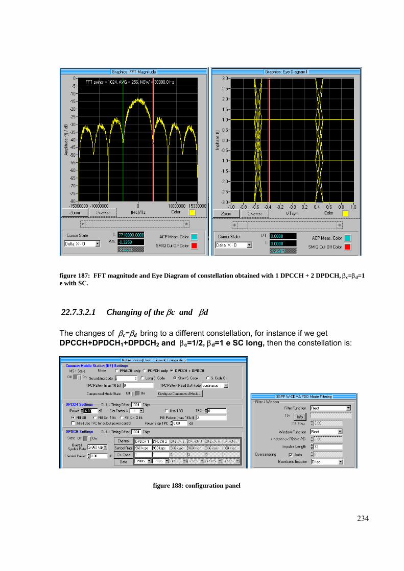
234
figure 187: FFT magnitude and Eye Diagram of constellation obtained with 1 DPCCH + 2 DPDCH, βc=βd=1 e with SC.
22.7.3.2.1 Changing of the βc and βd The changes of βc=βd bring to a different constellation, for instance if we get DPCCH+DPDCH1+DPDCH2 and βc=1/2, βd=1 e SC long, then the constellation is:
figure 188: configuration panel
S
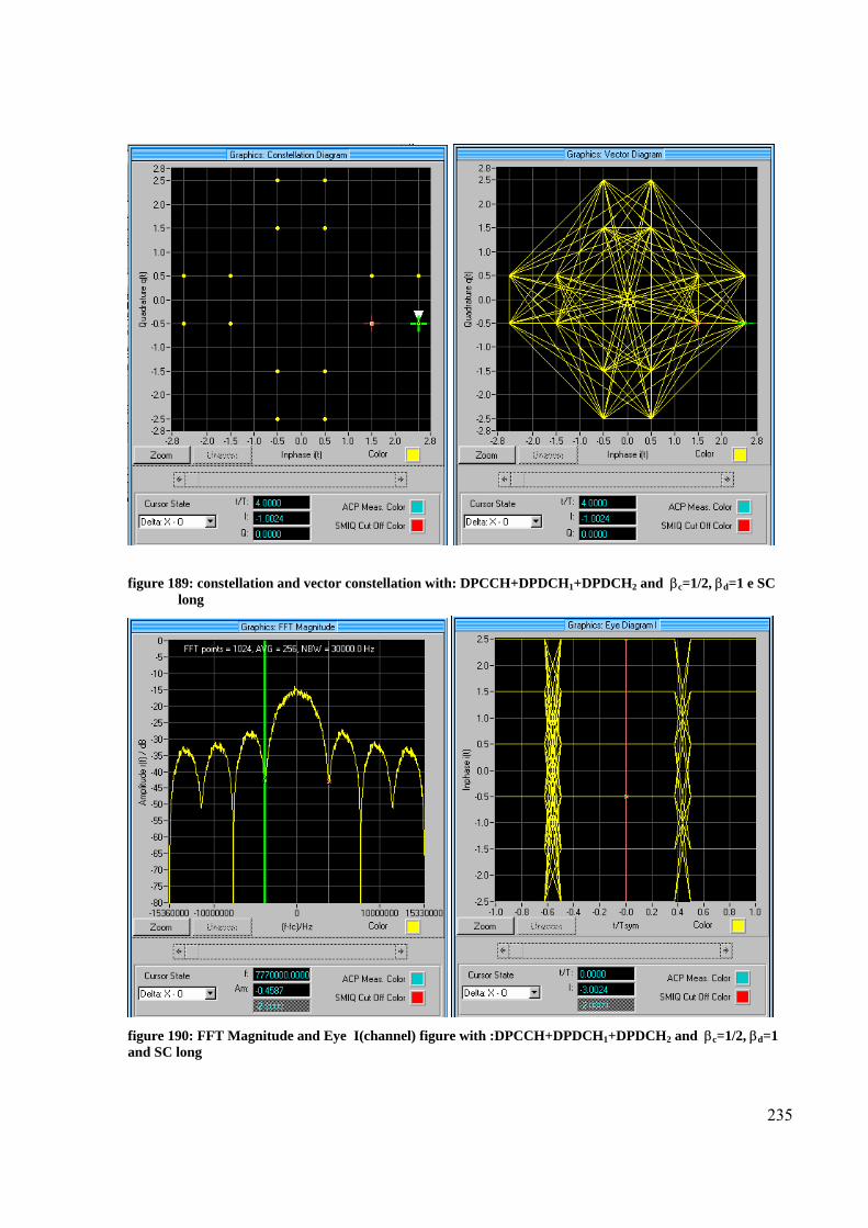
235
figure 189: constellation and vector constellation with: DPCCH+DPDCH1+DPDCH2 and βc=1/2, βd=1 e SC
long
figure 190: FFT Magnitude and Eye I(channel) figure with :DPCCH+DPDCH1+DPDCH2 and βc=1/2, βd=1 and SC long
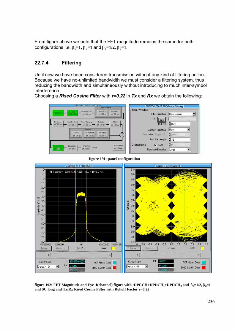
236
From figure above we note that the FFT magnitude remains the same for both configurations i.e. βc=1, βd=1 and βc=1/2, βd=1.
22.7.4 Filtering Until now we have been considered transmission without any kind of filtering action. Because we have no-unlimited bandwidth we must consider a filtering system, thus reducing the bandwidth and simultaneously without introducing to much inter-symbol interference. Choosing a Rised Cosine Filter with r=0.22 in Tx end Rx we obtain the following:
figure 191: panel configuration
figure 192: FFT Magnitude and Eye I(channel) figure with :DPCCH+DPDCH1+DPDCH2 and βc=1/2, βd=1 and SC long and Tx/Rx Rised Cosine Filter with Rolloff Factor r=0.22
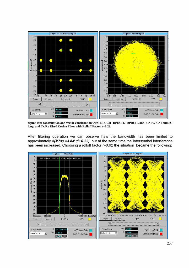
237
figure 193: constellation and vector constellation with: DPCCH+DPDCH1+DPDCH2 and βc=1/2, βd=1 and SC long and Tx/Rx Rised Cosine Filter with Rolloff Factor r=0.22.
After filtering operation we can observe haw the bandwidth has been limited to approximately 5(Mhz) ≅3.84*(1+0.22) but at the same time the Intersymbol interference has been increased. Choosing a rolloff factor r=0.62 the situation became the following:

238
22.8 Downlink Spreading and Modulation The spreading and scrambling concept for all downlink physical channels is illustrated in figure below.
figure 194 : spreading and scrambling scheme for all downlink physical channel
Apart from SCHs, each pair of to consecutive symbols is first serial-to-parallel converted and mapped onto I and Q branches. The I and Q branches are then spread to the chip rate by the same channelisation code Cch,SF,m. The sequence of real-valued chips on the I and Q branches are then scrambled using a complex-valued scrambling code, denoted Sdl,n . The scrambling code is applied aligned with the scrambling code applied to the P-CCPCH, where the first complex chip of the spread P-CCPCH frame is multiplied by chip number zero of the scrambling code. After spreading, each physical downlink channel (except SCHs) is separately weighted by a weigh factor, denoted Gi. The comlex-valued P-SCH and S-SCH are separately weighted by weight factor GP and GS. All downlink physical channel are combined using a complex addition and the resulting sequence generated by spreading and scrambling process is then QPSK modulated.
22.8.1 Downlink Spreading Codes In the downlink the same channelisation codes as in the uplink (OVSF codes) are used. Typically only one code tree per cell is used and the code tree under a single scrambling code is then shared between several users. By definition, the channelisation codes used for P-CPICH and P-CCPCH are Cch,256,0 and Cch,256,1 respectively. In compressed mode there are three methods for generating gaps:
J
cch,SF,m
Sdl,n
Cos(ωt)
I+jQ DL modulated signal
Any d-link phisical channel except SCH Q
IGS
SSerial to Parallel con
I Q
Gp
G1
G2
-sin(ωt)
P-SCH
S-SCH
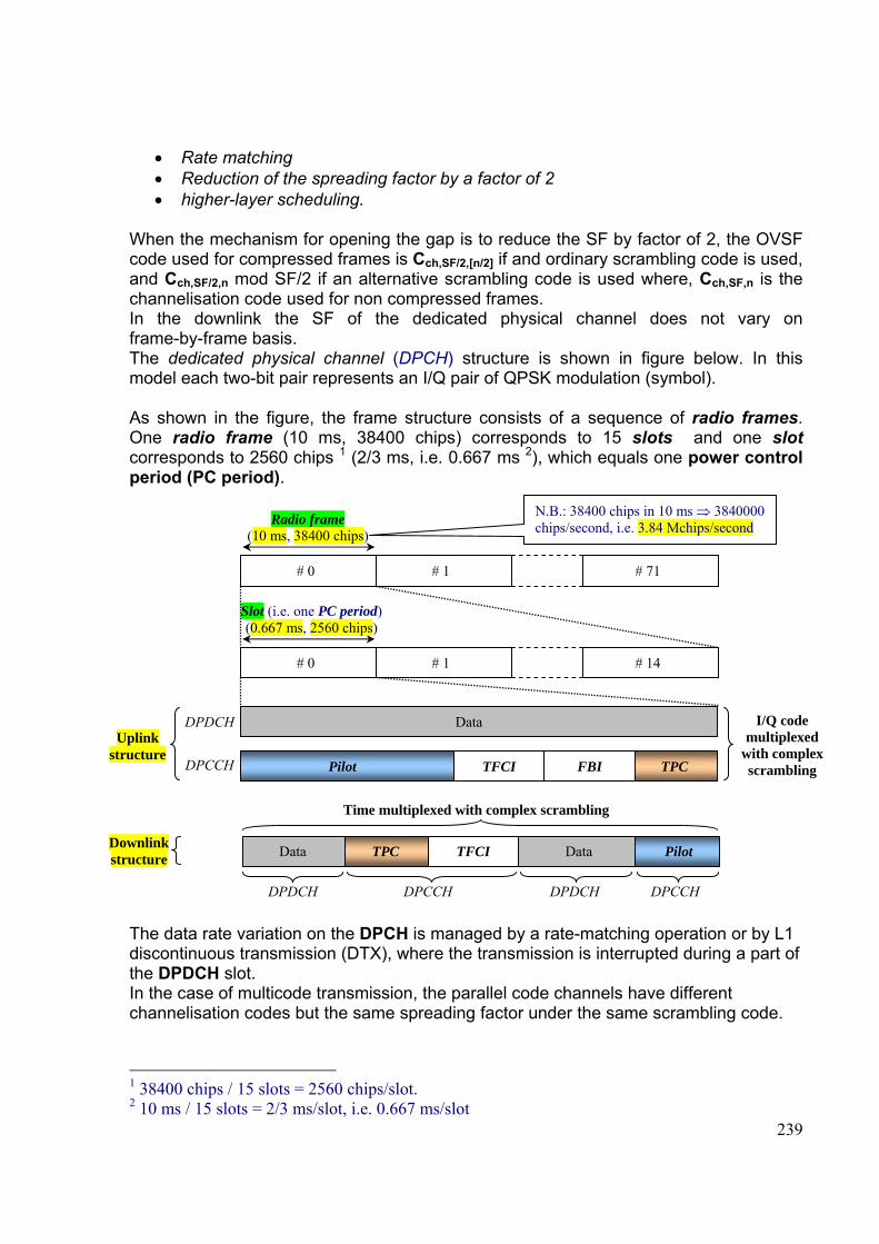
239
• Rate matching • Reduction of the spreading factor by a factor of 2 • higher-layer scheduling.
When the mechanism for opening the gap is to reduce the SF by factor of 2, the OVSF code used for compressed frames is Cch,SF/2,[n/2] if and ordinary scrambling code is used, and Cch,SF/2,n mod SF/2 if an alternative scrambling code is used where, Cch,SF,n is the channelisation code used for non compressed frames. In the downlink the SF of the dedicated physical channel does not vary on frame-by-frame basis. The dedicated physical channel (DPCH) structure is shown in figure below. In this model each two-bit pair represents an I/Q pair of QPSK modulation (symbol). As shown in the figure, the frame structure consists of a sequence of radio frames. One radio frame (10 ms, 38400 chips) corresponds to 15 slots and one slot corresponds to 2560 chips 1 (2/3 ms, i.e. 0.667 ms 2), which equals one power control period (PC period). The data rate variation on the DPCH is managed by a rate-matching operation or by L1 discontinuous transmission (DTX), where the transmission is interrupted during a part of the DPDCH slot. In the case of multicode transmission, the parallel code channels have different channelisation codes but the same spreading factor under the same scrambling code.
1 38400 chips / 15 slots = 2560 chips/slot. 2 10 ms / 15 slots = 2/3 ms/slot, i.e. 0.667 ms/slot
# 0
Radio frame (10 ms, 38400 chips)
# 1 # 71
# 0
Slot (i.e. one PC period) (0.667 ms, 2560 chips)
# 1 # 14
Data
Pilot TPC TFCI FBI
DPDCH
DPCCH
Uplink structure
I/Q code multiplexed
with complex scrambling
Time multiplexed with complex scrambling
DPDCH DPCCH
Downlink structure Data Pilot TPC TFCI Data
DPDCH DPCCH
N.B.: 38400 chips in 10 ms ⇒ 3840000 chips/second, i.e. 3.84 Mchips/second

240
Different spreading factors may employed in the case of several CCTrCHs received by the same UE. The OVSF code my vary from frame to frame on the PDSCH. The rule is that the OVSF code(s) below the smallest spreading factor is from the branch of the code tree pointed by the code with smallest spreading factor used for that connection.
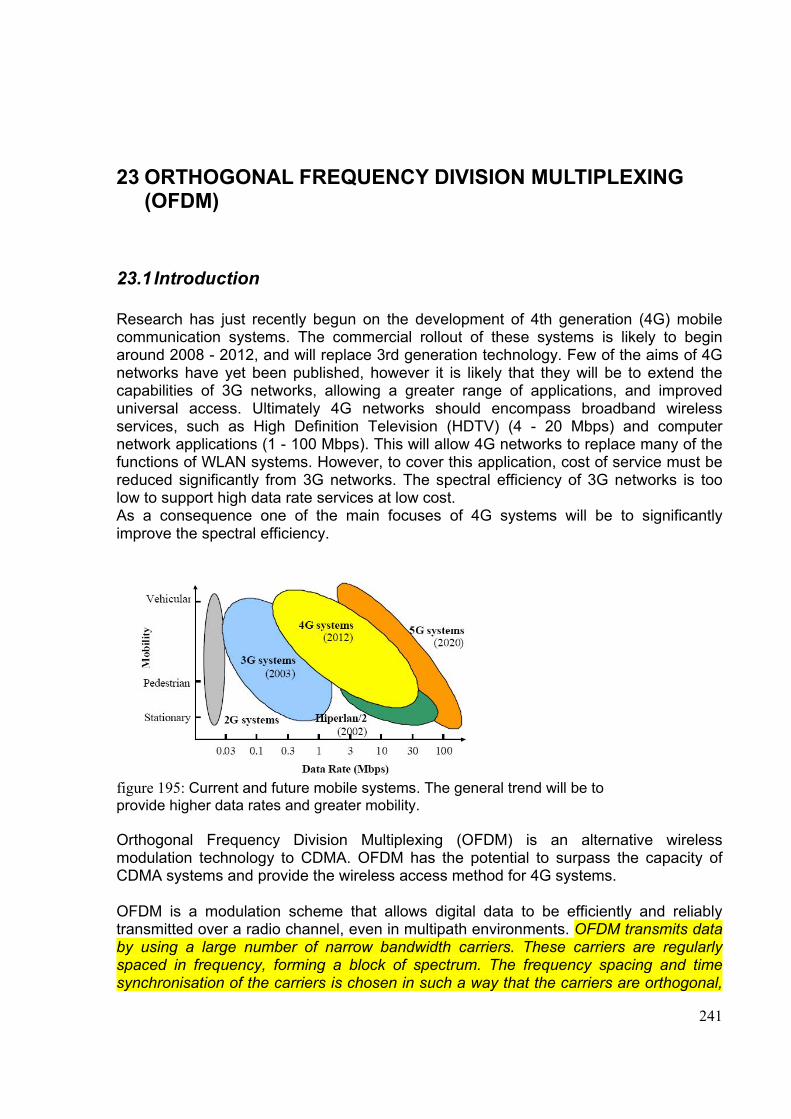
241
23 ORTHOGONAL FREQUENCY DIVISION MULTIPLEXING (OFDM)
23.1 Introduction Research has just recently begun on the development of 4th generation (4G) mobile communication systems. The commercial rollout of these systems is likely to begin around 2008 - 2012, and will replace 3rd generation technology. Few of the aims of 4G networks have yet been published, however it is likely that they will be to extend the capabilities of 3G networks, allowing a greater range of applications, and improved universal access. Ultimately 4G networks should encompass broadband wireless services, such as High Definition Television (HDTV) (4 - 20 Mbps) and computer network applications (1 - 100 Mbps). This will allow 4G networks to replace many of the functions of WLAN systems. However, to cover this application, cost of service must be reduced significantly from 3G networks. The spectral efficiency of 3G networks is too low to support high data rate services at low cost. As a consequence one of the main focuses of 4G systems will be to significantly improve the spectral efficiency.
figure 195: Current and future mobile systems. The general trend will be to provide higher data rates and greater mobility. Orthogonal Frequency Division Multiplexing (OFDM) is an alternative wireless modulation technology to CDMA. OFDM has the potential to surpass the capacity of CDMA systems and provide the wireless access method for 4G systems. OFDM is a modulation scheme that allows digital data to be efficiently and reliably transmitted over a radio channel, even in multipath environments. OFDM transmits data by using a large number of narrow bandwidth carriers. These carriers are regularly spaced in frequency, forming a block of spectrum. The frequency spacing and time synchronisation of the carriers is chosen in such a way that the carriers are orthogonal,

242
meaning that they do not cause interference to each other. This is despite the carriers overlapping each other in the frequency domain. The name ‘OFDM’ is derived from the fact that the digital data is sent using many carriers, each of a different frequency (Frequency Division Multiplexing) and these carriers are orthogonal to each other, hence Orthogonal Frequency Division Multiplexing. The origins of OFDM development started in the late 1950’s with the introduction of Frequency Division Multiplexing (FDM) for data communications. In 1966 Chang patented the structure of OFDM and published the concept of using orthogonal overlapping multi-tone signals for data communications. In 1971 Weinstein introduced the idea of using a Discrete Fourier Transform (DFT) for implementation of the generation and reception of OFDM signals, eliminating the requirement for banks of analog subcarrier oscillators. This presented an opportunity for an easy implementation of OFDM, especially with the use of Fast Fourier Transforms (FFT), which are an efficient implementation of the DFT. This suggested that the easiest implementation of OFDM is with the use of Digital Signal Processing (DSP), which can implement FFT algorithms. It is only recently that the advances in integrated circuit technology have made the implementation of OFDM cost effective. The reliance on DSP prevented the wide spread use of OFDM during the early development of FDM. It wasn’t until the late 1980’s that work began on the development of OFDM for ommercial use, with the introduction of the Digital Audio Broadcasting (DAB) system.
23.2 Digital Audio Broadcasting DAB was the first commercial use of OFDM technology. Development of DAB started in 1987 and services began in U.K and Sweden in 1995. DAB is a replacement for FM audio broadcasting, by providing high quality digital audio and information services. OFDM was used for DAB due to its multipath tolerance. Broadcast systems operate with potentially very long transmission distances (20 -100 km). As a result, multipath is a major problem as it causes extensive ghosting of the transmission. This ghosting causes Inter-Symbol Interference (ISI), blurring the time domain signal. For single carrier transmissions the effects of ISI are normally mitigated using adaptive equalisation. This process uses adaptive filtering to approximate the impulse response of the radio channel. An inverse channel response filter is then used to recombine the blurred copies of the symbol bits. This process is however complex and slow due to the locking time of the adaptive equaliser. Additionally it becomes increasing difficult to equalise signals that suffer ISI of more than a couple of symbol periods. OFDM overcomes the effects of multipath by breaking the signal into many narrow bandwidth carriers. This results in a low symbol rate reducing the amount of ISI. In addition to this, a guard period is added to the start of each symbol, removing the effects of ISI for multipath signals delayed less than the guard period. The high tolerance to multipath makes OFDM more suited to high data transmissions in terrestrial environments than single carrier transmissions.
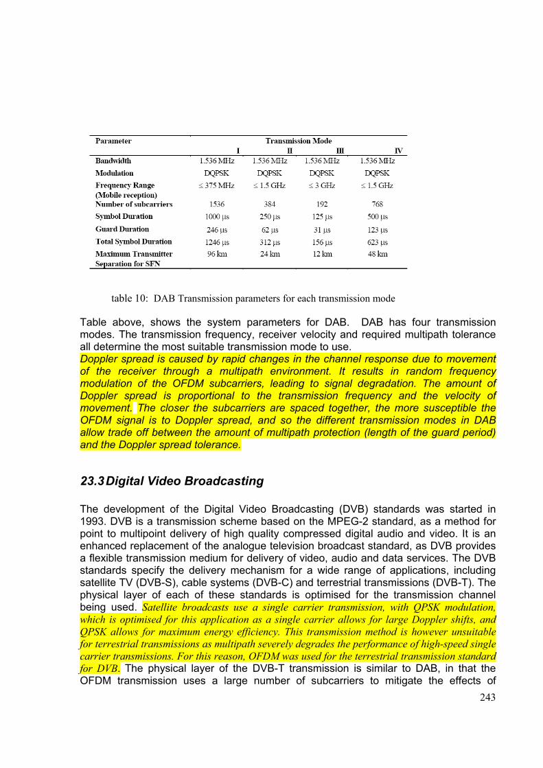
243
table 10: DAB Transmission parameters for each transmission mode
Table above, shows the system parameters for DAB. DAB has four transmission modes. The transmission frequency, receiver velocity and required multipath tolerance all determine the most suitable transmission mode to use. Doppler spread is caused by rapid changes in the channel response due to movement of the receiver through a multipath environment. It results in random frequency modulation of the OFDM subcarriers, leading to signal degradation. The amount of Doppler spread is proportional to the transmission frequency and the velocity of movement. The closer the subcarriers are spaced together, the more susceptible the OFDM signal is to Doppler spread, and so the different transmission modes in DAB allow trade off between the amount of multipath protection (length of the guard period) and the Doppler spread tolerance.
23.3 Digital Video Broadcasting The development of the Digital Video Broadcasting (DVB) standards was started in 1993. DVB is a transmission scheme based on the MPEG-2 standard, as a method for point to multipoint delivery of high quality compressed digital audio and video. It is an enhanced replacement of the analogue television broadcast standard, as DVB provides a flexible transmission medium for delivery of video, audio and data services. The DVB standards specify the delivery mechanism for a wide range of applications, including satellite TV (DVB-S), cable systems (DVB-C) and terrestrial transmissions (DVB-T). The physical layer of each of these standards is optimised for the transmission channel being used. Satellite broadcasts use a single carrier transmission, with QPSK modulation, which is optimised for this application as a single carrier allows for large Doppler shifts, and QPSK allows for maximum energy efficiency. This transmission method is however unsuitable for terrestrial transmissions as multipath severely degrades the performance of high-speed single carrier transmissions. For this reason, OFDM was used for the terrestrial transmission standard for DVB. The physical layer of the DVB-T transmission is similar to DAB, in that the OFDM transmission uses a large number of subcarriers to mitigate the effects of
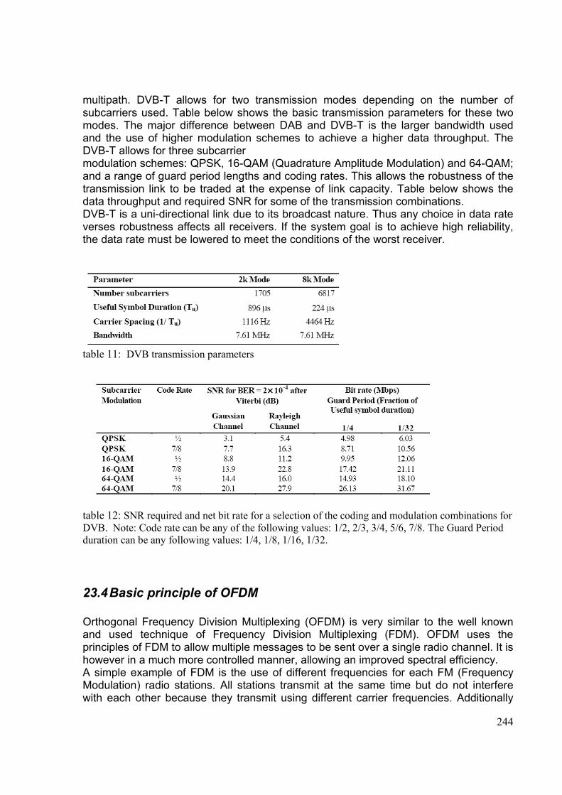
244
multipath. DVB-T allows for two transmission modes depending on the number of subcarriers used. Table below shows the basic transmission parameters for these two modes. The major difference between DAB and DVB-T is the larger bandwidth used and the use of higher modulation schemes to achieve a higher data throughput. The DVB-T allows for three subcarrier modulation schemes: QPSK, 16-QAM (Quadrature Amplitude Modulation) and 64-QAM; and a range of guard period lengths and coding rates. This allows the robustness of the transmission link to be traded at the expense of link capacity. Table below shows the data throughput and required SNR for some of the transmission combinations. DVB-T is a uni-directional link due to its broadcast nature. Thus any choice in data rate verses robustness affects all receivers. If the system goal is to achieve high reliability, the data rate must be lowered to meet the conditions of the worst receiver.
table 11: DVB transmission parameters
table 12: SNR required and net bit rate for a selection of the coding and modulation combinations for DVB. Note: Code rate can be any of the following values: 1/2, 2/3, 3/4, 5/6, 7/8. The Guard Period duration can be any following values: 1/4, 1/8, 1/16, 1/32.
23.4 Basic principle of OFDM Orthogonal Frequency Division Multiplexing (OFDM) is very similar to the well known and used technique of Frequency Division Multiplexing (FDM). OFDM uses the principles of FDM to allow multiple messages to be sent over a single radio channel. It is however in a much more controlled manner, allowing an improved spectral efficiency. A simple example of FDM is the use of different frequencies for each FM (Frequency Modulation) radio stations. All stations transmit at the same time but do not interfere with each other because they transmit using different carrier frequencies. Additionally
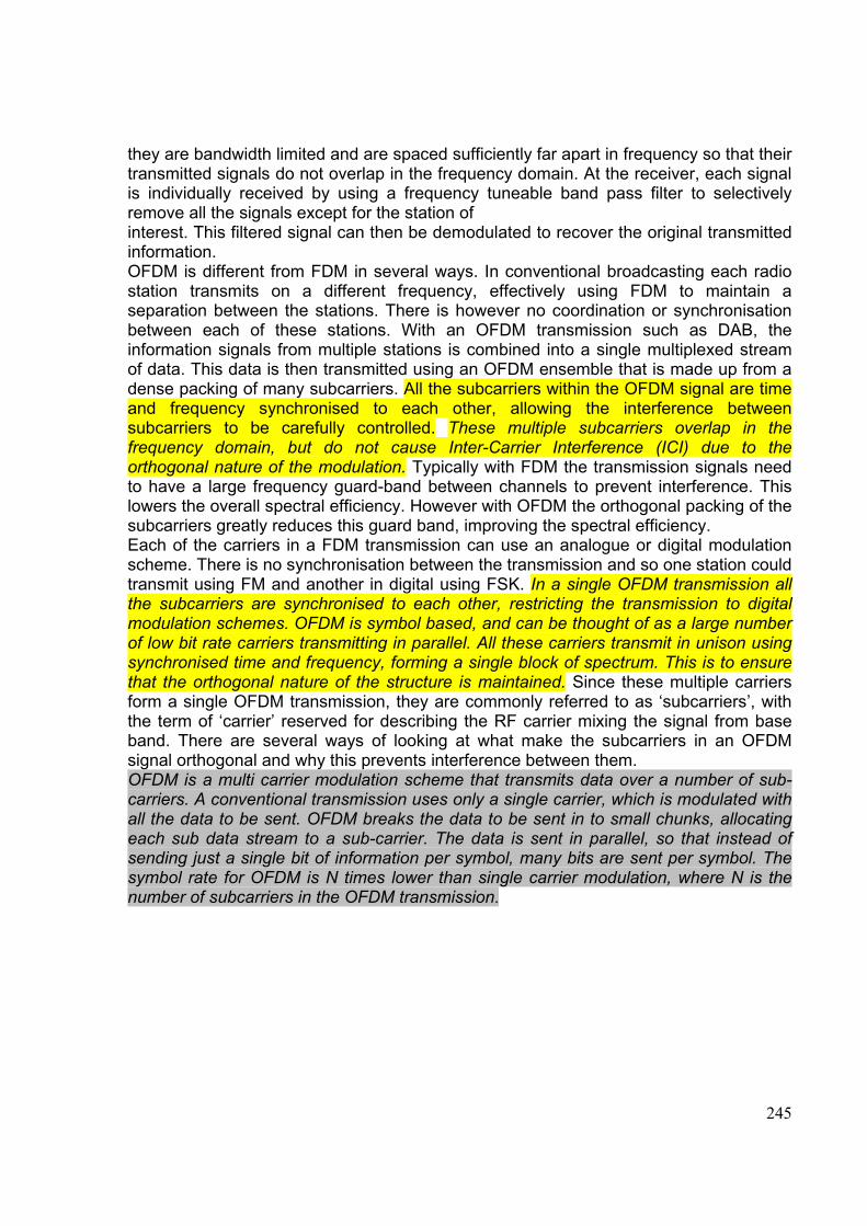
245
they are bandwidth limited and are spaced sufficiently far apart in frequency so that their transmitted signals do not overlap in the frequency domain. At the receiver, each signal is individually received by using a frequency tuneable band pass filter to selectively remove all the signals except for the station of interest. This filtered signal can then be demodulated to recover the original transmitted information. OFDM is different from FDM in several ways. In conventional broadcasting each radio station transmits on a different frequency, effectively using FDM to maintain a separation between the stations. There is however no coordination or synchronisation between each of these stations. With an OFDM transmission such as DAB, the information signals from multiple stations is combined into a single multiplexed stream of data. This data is then transmitted using an OFDM ensemble that is made up from a dense packing of many subcarriers. All the subcarriers within the OFDM signal are time and frequency synchronised to each other, allowing the interference between subcarriers to be carefully controlled. These multiple subcarriers overlap in the frequency domain, but do not cause Inter-Carrier Interference (ICI) due to the orthogonal nature of the modulation. Typically with FDM the transmission signals need to have a large frequency guard-band between channels to prevent interference. This lowers the overall spectral efficiency. However with OFDM the orthogonal packing of the subcarriers greatly reduces this guard band, improving the spectral efficiency. Each of the carriers in a FDM transmission can use an analogue or digital modulation scheme. There is no synchronisation between the transmission and so one station could transmit using FM and another in digital using FSK. In a single OFDM transmission all the subcarriers are synchronised to each other, restricting the transmission to digital modulation schemes. OFDM is symbol based, and can be thought of as a large number of low bit rate carriers transmitting in parallel. All these carriers transmit in unison using synchronised time and frequency, forming a single block of spectrum. This is to ensure that the orthogonal nature of the structure is maintained. Since these multiple carriers form a single OFDM transmission, they are commonly referred to as ‘subcarriers’, with the term of ‘carrier’ reserved for describing the RF carrier mixing the signal from base band. There are several ways of looking at what make the subcarriers in an OFDM signal orthogonal and why this prevents interference between them. OFDM is a multi carrier modulation scheme that transmits data over a number of sub-carriers. A conventional transmission uses only a single carrier, which is modulated with all the data to be sent. OFDM breaks the data to be sent in to small chunks, allocating each sub data stream to a sub-carrier. The data is sent in parallel, so that instead of sending just a single bit of information per symbol, many bits are sent per symbol. The symbol rate for OFDM is N times lower than single carrier modulation, where N is the number of subcarriers in the OFDM transmission.
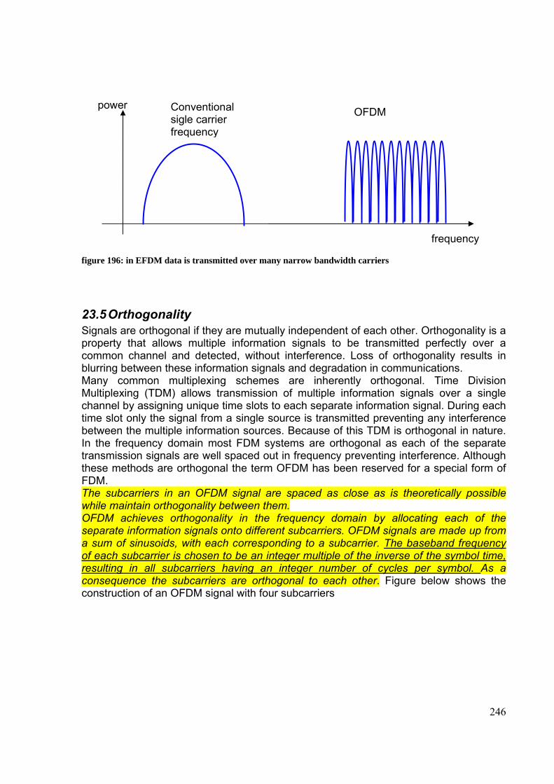
246
figure 196: in EFDM data is transmitted over many narrow bandwidth carriers
23.5 Orthogonality Signals are orthogonal if they are mutually independent of each other. Orthogonality is a property that allows multiple information signals to be transmitted perfectly over a common channel and detected, without interference. Loss of orthogonality results in blurring between these information signals and degradation in communications. Many common multiplexing schemes are inherently orthogonal. Time Division Multiplexing (TDM) allows transmission of multiple information signals over a single channel by assigning unique time slots to each separate information signal. During each time slot only the signal from a single source is transmitted preventing any interference between the multiple information sources. Because of this TDM is orthogonal in nature. In the frequency domain most FDM systems are orthogonal as each of the separate transmission signals are well spaced out in frequency preventing interference. Although these methods are orthogonal the term OFDM has been reserved for a special form of FDM. The subcarriers in an OFDM signal are spaced as close as is theoretically possible while maintain orthogonality between them. OFDM achieves orthogonality in the frequency domain by allocating each of the separate information signals onto different subcarriers. OFDM signals are made up from a sum of sinusoids, with each corresponding to a subcarrier. The baseband frequency of each subcarrier is chosen to be an integer multiple of the inverse of the symbol time, resulting in all subcarriers having an integer number of cycles per symbol. As a consequence the subcarriers are orthogonal to each other. Figure below shows the construction of an OFDM signal with four subcarriers
Conventional sigle carrier frequency
OFDM
frequency
power
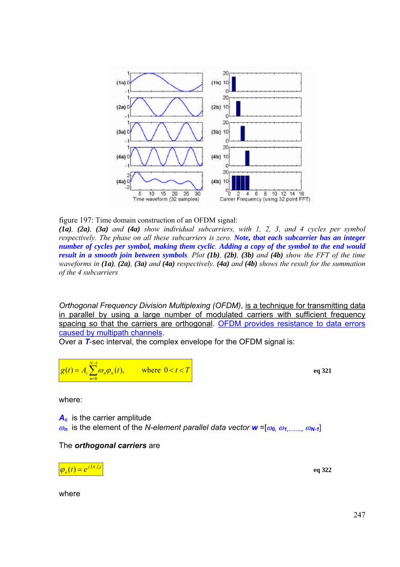
247
figure 197: Time domain construction of an OFDM signal: (1a), (2a), (3a) and (4a) show individual subcarriers, with 1, 2, 3, and 4 cycles per symbol respectively. The phase on all these subcarriers is zero. Note, that each subcarrier has an integer number of cycles per symbol, making them cyclic. Adding a copy of the symbol to the end would result in a smooth join between symbols. Plot (1b), (2b), (3b) and (4b) show the FFT of the time waveforms in (1a), (2a), (3a) and (4a) respectively. (4a) and (4b) shows the result for the summation of the 4 subcarriers
Orthogonal Frequency Division Multiplexing (OFDM), is a technique for transmitting data in parallel by using a large number of modulated carriers with sufficient frequency spacing so that the carriers are orthogonal. OFDM provides resistance to data errors caused by multipath channels. Over a T-sec interval, the complex envelope for the OFDM signal is:
TttAtgN
nnnc <<= ∑
−
=
0 here w,)()(1
0ϕω eq 321
where: Ac is the carrier amplitude ωn is the element of the N-element parallel data vector w =[ω0, ω1,…….., ωN-1] The orthogonal carriers are
tfjn
net πϕ 2)( = eq 322
where
248
⎪⎪⎭
⎪⎪⎬
⎫
⎪⎪⎩
⎪⎪⎨
⎧
⎟⎠⎞
⎜⎝⎛ −+=⇒−=
⎟⎠⎞
⎜⎝⎛ −−=⇒=
⇒⎟⎠⎞
⎜⎝⎛ −
−=
211 1
211 0
2
11N
TfNnfor
NT
fnforNn
Tf
n
n
n eq 323
The duration of the data symbol on each carrier is T seconds, and carriers are spaced 1/T Hz apart in fact:
TNn
TNn
Tff nn
1 2
112
1111 =⎟
⎠⎞
⎜⎝⎛ −
−−⎟⎠⎞
⎜⎝⎛ −
−+=−+ eq 324
This assures that the carriers are orthogonal, since ϕn(t) satisfy the orthogonality condition over the T-sec interval:
0)()( * =∫ dttt m
b
an ϕϕ eq 325
in fact recalling that: ⎟⎠⎞
⎜⎝⎛ −
−=⎟⎠⎞
⎜⎝⎛ −
−=2
11 and 2
11 NmT
fNnT
f mn with n≠m consequently:
( )
( )
( )
( )
( )( )[ ]
( )( )[ ] ( )[ ][ ]
( )[ ] 011
12
1
12sin2cos12
1112
1
112
112
1
211
2112
1
)(2)(2
1
0)()(
2
12
0
12
0
211
2112
0
)(2
0
)(22
0
2
*
=−
⎥⎦⎤
⎢⎣⎡ −
=
−−+−
⎥⎦⎤
⎢⎣⎡ −
=−
⎥⎦⎤
⎢⎣⎡ −
=
=⎥⎥⎦
⎤
⎢⎢⎣
⎡−
⎥⎦⎤
⎢⎣⎡ −
=⎥⎥⎦
⎤
⎢⎢⎣
⎡
⎥⎦⎤
⎢⎣⎡ −
=⎥⎥⎦
⎤
⎢⎢⎣
⎡
⎥⎦
⎤⎢⎣
⎡⎟⎠⎞
⎜⎝⎛ −
−−⎟⎠⎞
⎜⎝⎛ −
−
=−−
==⇒
=
−
⎥⎦⎤
⎢⎣⎡ −⎥⎦
⎤⎢⎣⎡ −
⎥⎦
⎤⎢⎣
⎡⎟⎠⎞
⎜⎝⎛ −
−−⎟⎠⎞
⎜⎝⎛ −
−
−−− ∫∫∫
∫
mnT
j
mnjmnmn
Tj
emn
Tj
emn
Tj
emn
Tj
eNm
TNn
Tj
effjffj
dtedtee
dttt
mnj
TmnT
jT
tmnT
j
TtNm
TNn
Tj
Ttffj
mnmn
Ttffjtfj
Ttfj
m
b
an
mnmnmn
π
ππππ
ππ
π
ππ
ϕϕ
π
ππ
π
ππππ
eq 326
249
Because the carriers are orthogonal, data can be detected on each of these closely spaced carriers without interference from the other carriers. Another way of thinking to orthogonality concept is that if we look at a matched receiver for one of the orthogonal functions, a subcarrier in the case of OFDM, then the receiver will only see the result for that function. The results from all other functions in the set integrate to zero, and thus have no effect. Equation below shows a set of orthogonal sinusoids, which represent the subcarriers for an unmodulated real OFDM signal.
⎭⎬⎫
⎩⎨⎧ =<<
=otherwise
MkTttkftsk 0
,......2,10)2sin()( 0π
eq 327
Where f0 is the carrier spacing, M is the number of carriers, T is the symbol period. Since the highest frequency component is Mf0 the transmission bandwidth is also Mf0. These subcarriers are orthogonal to each other because when we multiply the waveforms of any two subcarriers and integrate over the symbol period the result is zero. Multiplying the two sine waves together is the same as mixing these subcarriers. This results in sum and difference frequency components, which will always be integer subcarrier frequencies, as the frequency of the two mixing subcarriers has integer number of cycles. Since the system is linear we can integrate the result by taking the integral of each frequency component separately then combining the results by adding the two sub-integrals. The two frequency components after the mixing have an integer number of cycles over the period and so the sub-integral of each component will be zero, as the integral of a sinusoid over an entire period is zero. Both the sub-integrals are zeros and so the resulting addition of the two will also be zero, thus we have established that the frequency components are orthogonal to each other.
23.5.1 FREQUENCY DOMAIN ORTHOGONALITY Another way to view the orthogonality property of OFDM signals is to look at its spectrum. In the frequency domain each OFDM subcarrier has a sinc, sin(x)/x, frequency response, as shown in Figure below. This is a result of the symbol time corresponding to the inverse of the carrier spacing. As far as the receiver is concerned each OFDM symbol transmitted for a fixed time (TFFT) with no tapering at the ends of the symbol. This symbol time corresponds to the inverse of the subcarrier spacing of 1/TFFT Hz 1. This rectangular, boxcar, waveform in the time domain results in a sinc frequency response in the frequency domain. The sinc shape has a narrow main lobe, with many side-lobes that decay slowly with the magnitude of the frequency difference away from the centre. Each carrier has a peak at the centre frequency and nulls evenly spaced with a frequency gap equal to the carrier spacing. The orthogonal nature of the transmission is a result of the peak of each subcarrier corresponding to the nulls of all other subcarriers. When this signal is detected using
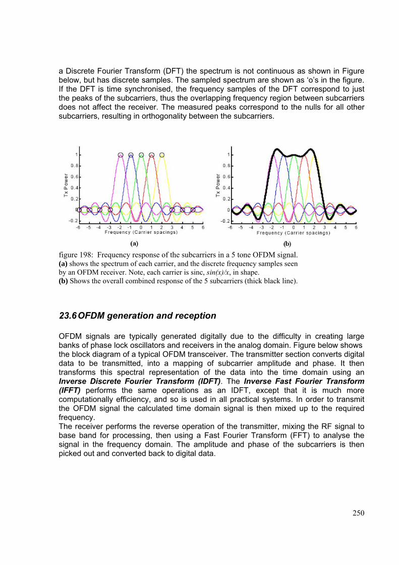
250
a Discrete Fourier Transform (DFT) the spectrum is not continuous as shown in Figure below, but has discrete samples. The sampled spectrum are shown as ‘o’s in the figure. If the DFT is time synchronised, the frequency samples of the DFT correspond to just the peaks of the subcarriers, thus the overlapping frequency region between subcarriers does not affect the receiver. The measured peaks correspond to the nulls for all other subcarriers, resulting in orthogonality between the subcarriers.
figure 198: Frequency response of the subcarriers in a 5 tone OFDM signal. (a) shows the spectrum of each carrier, and the discrete frequency samples seen by an OFDM receiver. Note, each carrier is sinc, sin(x)/x, in shape. (b) Shows the overall combined response of the 5 subcarriers (thick black line).
23.6 OFDM generation and reception OFDM signals are typically generated digitally due to the difficulty in creating large banks of phase lock oscillators and receivers in the analog domain. Figure below shows the block diagram of a typical OFDM transceiver. The transmitter section converts digital data to be transmitted, into a mapping of subcarrier amplitude and phase. It then transforms this spectral representation of the data into the time domain using an Inverse Discrete Fourier Transform (IDFT). The Inverse Fast Fourier Transform (IFFT) performs the same operations as an IDFT, except that it is much more computationally efficiency, and so is used in all practical systems. In order to transmit the OFDM signal the calculated time domain signal is then mixed up to the required frequency. The receiver performs the reverse operation of the transmitter, mixing the RF signal to base band for processing, then using a Fast Fourier Transform (FFT) to analyse the signal in the frequency domain. The amplitude and phase of the subcarriers is then picked out and converted back to digital data.
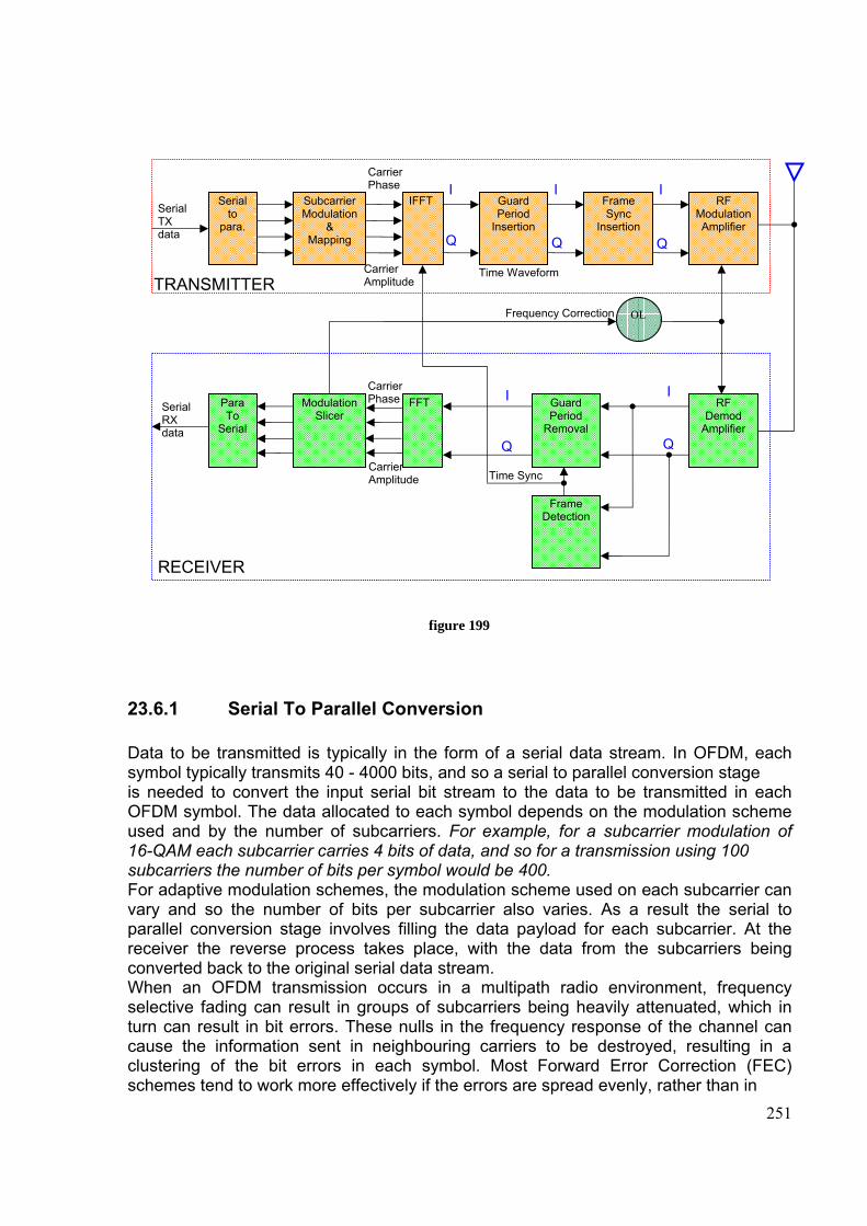
251
figure 199
23.6.1 Serial To Parallel Conversion Data to be transmitted is typically in the form of a serial data stream. In OFDM, each symbol typically transmits 40 - 4000 bits, and so a serial to parallel conversion stage is needed to convert the input serial bit stream to the data to be transmitted in each OFDM symbol. The data allocated to each symbol depends on the modulation scheme used and by the number of subcarriers. For example, for a subcarrier modulation of 16-QAM each subcarrier carries 4 bits of data, and so for a transmission using 100 subcarriers the number of bits per symbol would be 400. For adaptive modulation schemes, the modulation scheme used on each subcarrier can vary and so the number of bits per subcarrier also varies. As a result the serial to parallel conversion stage involves filling the data payload for each subcarrier. At the receiver the reverse process takes place, with the data from the subcarriers being converted back to the original serial data stream. When an OFDM transmission occurs in a multipath radio environment, frequency selective fading can result in groups of subcarriers being heavily attenuated, which in turn can result in bit errors. These nulls in the frequency response of the channel can cause the information sent in neighbouring carriers to be destroyed, resulting in a clustering of the bit errors in each symbol. Most Forward Error Correction (FEC) schemes tend to work more effectively if the errors are spread evenly, rather than in
Frequency Correction
Time Waveform
Carrier Amplitude
Carrier Phase
Serial to
para.
SubcarrierModulation
& Mapping
IFFT Guard Period
Insertion
Frame Sync
Insertion
RF Modulation Amplifier
Para To
Serial
Modulation Slicer
FFT Guard Period
Removal
Frame Detection
RF Demod
Amplifier
Serial TX data
Carrier Amplitude
Carrier Phase I I I
I I
Q Q Q
Q Q
Serial RX data
Time Sync
OL
RECEIVER
TRANSMITTER
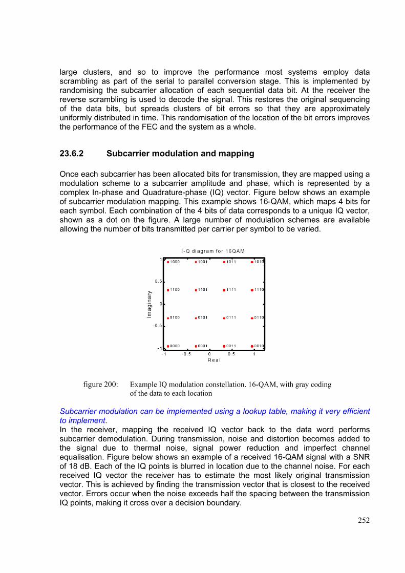
252
large clusters, and so to improve the performance most systems employ data scrambling as part of the serial to parallel conversion stage. This is implemented by randomising the subcarrier allocation of each sequential data bit. At the receiver the reverse scrambling is used to decode the signal. This restores the original sequencing of the data bits, but spreads clusters of bit errors so that they are approximately uniformly distributed in time. This randomisation of the location of the bit errors improves the performance of the FEC and the system as a whole.
23.6.2 Subcarrier modulation and mapping Once each subcarrier has been allocated bits for transmission, they are mapped using a modulation scheme to a subcarrier amplitude and phase, which is represented by a complex In-phase and Quadrature-phase (IQ) vector. Figure below shows an example of subcarrier modulation mapping. This example shows 16-QAM, which maps 4 bits for each symbol. Each combination of the 4 bits of data corresponds to a unique IQ vector, shown as a dot on the figure. A large number of modulation schemes are available allowing the number of bits transmitted per carrier per symbol to be varied.
figure 200: Example IQ modulation constellation. 16-QAM, with gray coding of the data to each location
Subcarrier modulation can be implemented using a lookup table, making it very efficient to implement. In the receiver, mapping the received IQ vector back to the data word performs subcarrier demodulation. During transmission, noise and distortion becomes added to the signal due to thermal noise, signal power reduction and imperfect channel equalisation. Figure below shows an example of a received 16-QAM signal with a SNR of 18 dB. Each of the IQ points is blurred in location due to the channel noise. For each received IQ vector the receiver has to estimate the most likely original transmission vector. This is achieved by finding the transmission vector that is closest to the received vector. Errors occur when the noise exceeds half the spacing between the transmission IQ points, making it cross over a decision boundary.
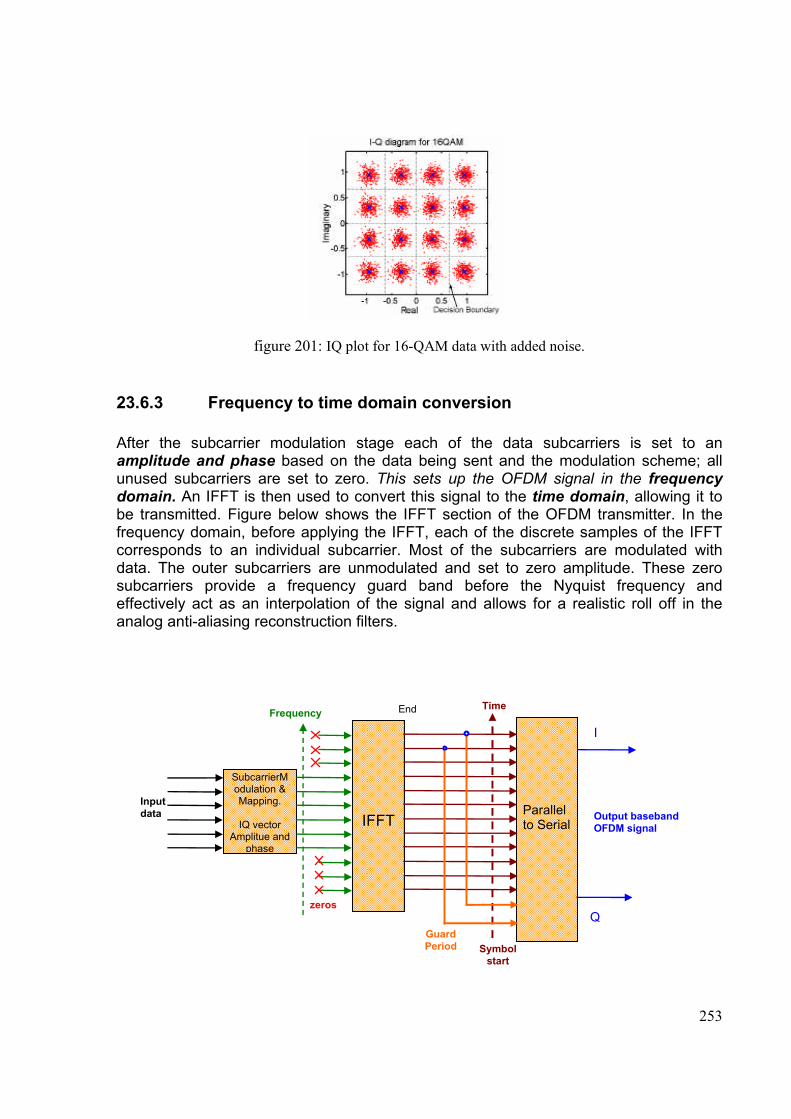
253
figure 201: IQ plot for 16-QAM data with added noise.
23.6.3 Frequency to time domain conversion After the subcarrier modulation stage each of the data subcarriers is set to an amplitude and phase based on the data being sent and the modulation scheme; all unused subcarriers are set to zero. This sets up the OFDM signal in the frequency domain. An IFFT is then used to convert this signal to the time domain, allowing it to be transmitted. Figure below shows the IFFT section of the OFDM transmitter. In the frequency domain, before applying the IFFT, each of the discrete samples of the IFFT corresponds to an individual subcarrier. Most of the subcarriers are modulated with data. The outer subcarriers are unmodulated and set to zero amplitude. These zero subcarriers provide a frequency guard band before the Nyquist frequency and effectively act as an interpolation of the signal and allows for a realistic roll off in the analog anti-aliasing reconstruction filters.
Symbol start
SubcarrierModulation & Mapping.
IQ vector
Amplitue and phase
IFFT
Parallel to Serial
Input data
Guard Period
End
I
Q zeros
Frequency Time
Output baseband OFDM signal
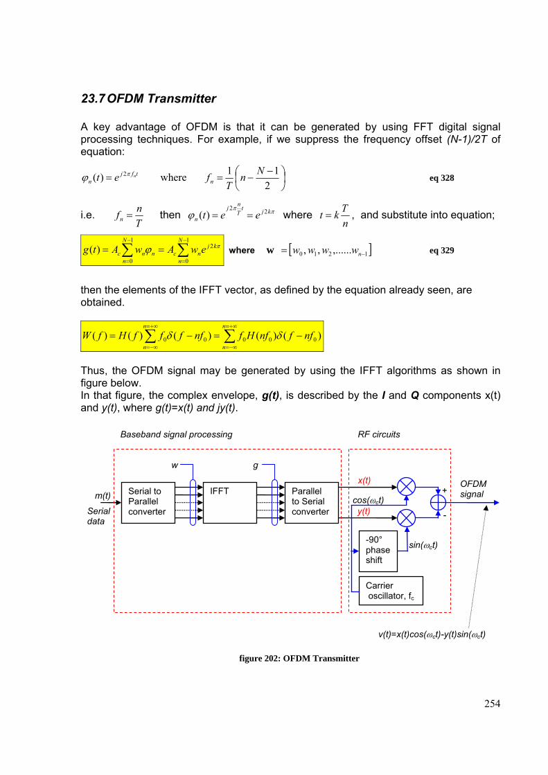
254
23.7 OFDM Transmitter A key advantage of OFDM is that it can be generated by using FFT digital signal processing techniques. For example, if we suppress the frequency offset (N-1)/2T of equation:
⎟⎠⎞
⎜⎝⎛ −
−==2
11 ere wh)( 2 NnT
fet ntfj
nnπϕ eq 328
i.e. Tnfn = then ππ
ϕ kjtTnj
n eet 22)( == where
nTkt = , and substitute into equation;
∑ ∑−
=
−
=
==1
0
1
0
2)(N
n
N
n
kjncnnc ewAwAtg πϕ where [ ]1210 ,......,, −= nwwwww eq 329
then the elements of the IFFT vector, as defined by the equation already seen, are obtained.
∑∑+∞=
−∞=
+∞=
−∞=
−=−=n
n
n
n
nffnfHfnffffHfW )()()()()( 00000 δδ
Thus, the OFDM signal may be generated by using the IFFT algorithms as shown in figure below. In that figure, the complex envelope, g(t), is described by the I and Q components x(t) and y(t), where g(t)=x(t) and jy(t).
figure 202: OFDM Transmitter
v(t)=x(t)cos(ωct)-y(t)sin(ωct)
Serial to Parallel converter
m(t) IFFT
w g
Parallel to Serial converter
+
-
-90° phase shift
Carrier oscillator, fc
Baseband signal processing RF circuits
cos(ωct)
sin(ωct)
OFDM signal
Serial data
x(t)
y(t)
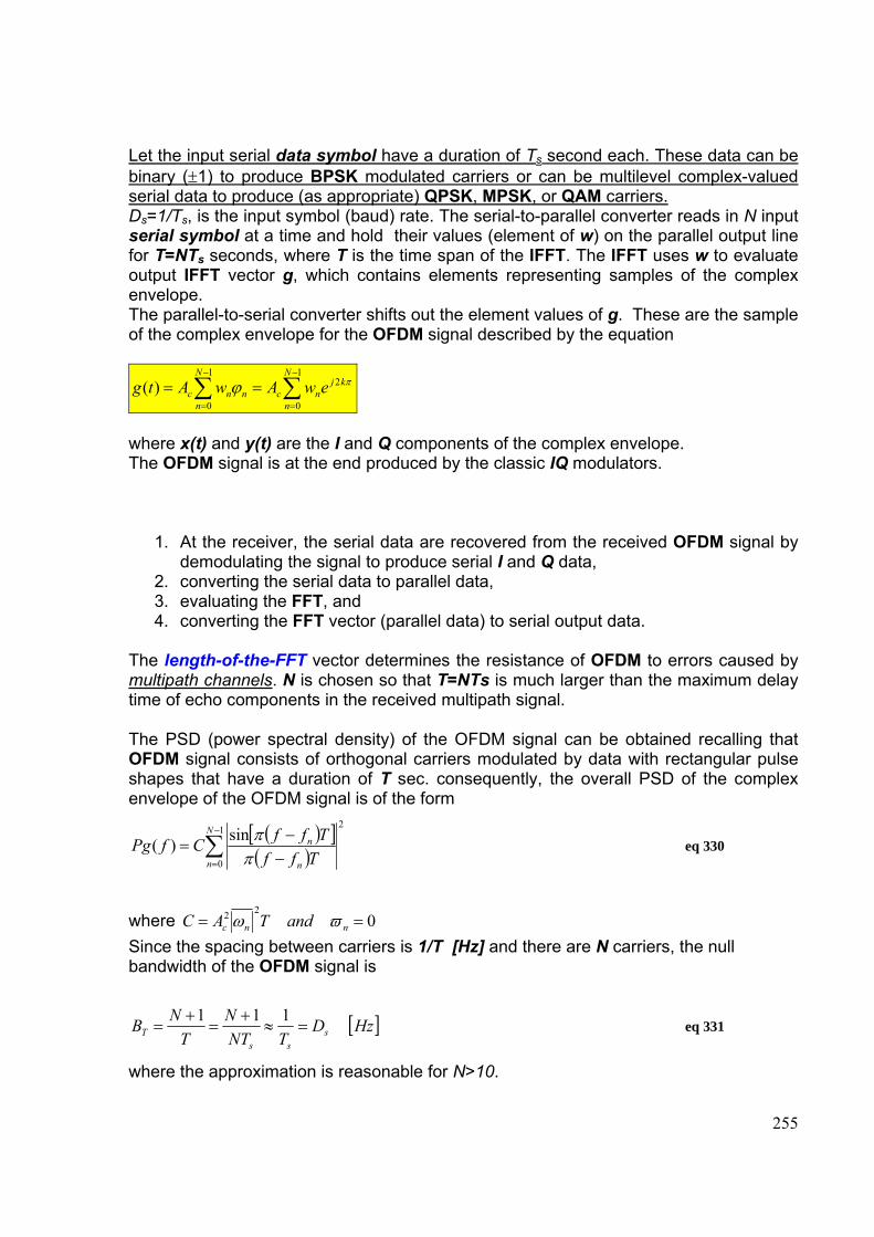
255
Let the input serial data symbol have a duration of Ts second each. These data can be binary (±1) to produce BPSK modulated carriers or can be multilevel complex-valued serial data to produce (as appropriate) QPSK, MPSK, or QAM carriers. Ds=1/Ts, is the input symbol (baud) rate. The serial-to-parallel converter reads in N input serial symbol at a time and hold their values (element of w) on the parallel output line for T=NTs seconds, where T is the time span of the IFFT. The IFFT uses w to evaluate output IFFT vector g, which contains elements representing samples of the complex envelope. The parallel-to-serial converter shifts out the element values of g. These are the sample of the complex envelope for the OFDM signal described by the equation
∑ ∑−
=
−
=
==1
0
1
0
2)(N
n
N
n
kjncnnc ewAwAtg πϕ
where x(t) and y(t) are the I and Q components of the complex envelope. The OFDM signal is at the end produced by the classic IQ modulators.
1. At the receiver, the serial data are recovered from the received OFDM signal by demodulating the signal to produce serial I and Q data,
2. converting the serial data to parallel data, 3. evaluating the FFT, and 4. converting the FFT vector (parallel data) to serial output data.
The length-of-the-FFT vector determines the resistance of OFDM to errors caused by multipath channels. N is chosen so that T=NTs is much larger than the maximum delay time of echo components in the received multipath signal. The PSD (power spectral density) of the OFDM signal can be obtained recalling that OFDM signal consists of orthogonal carriers modulated by data with rectangular pulse shapes that have a duration of T sec. consequently, the overall PSD of the complex envelope of the OFDM signal is of the form
( )[ ]( )
21
0
sin)( ∑−
= −−
=N
n n
n
TffTffCfPg
ππ
eq 330
where 0
22 == nnc andTAC ϖω Since the spacing between carriers is 1/T [Hz] and there are N carriers, the null bandwidth of the OFDM signal is
[ ]HzDTNT
NT
NB sss
T 111 =≈
+=
+= eq 331
where the approximation is reasonable for N>10.
256
A key advantage of OFDM is that it can be generated by using FFT digital signal processing techniques. An Example of FFT theory is reported in the following paragraph.
23.8 FFT(Line Specra for Periodic Waveforms) For periodic waveforms, the Fourier series representations are valid over all time (i.e.-∞<t<+∞). Consequently, the (two sided) spectrum, which depends on the waveshape from t=-∞ to t=∞, my be evaluated in terms of Fourier coefficients.
23.8.1 Theorem If a waveform is periodic with period T0, the spectrum of the waveform w(t) is:
( ) [ ]∑+∞=
−∞=
=−=n
nn twFnffcfW )()( 0δ eq 332
Where: f0=1/T0, ω0=2π f0=2π /T0,
∫+
−=0
0)(1
0
Ta
a
tjnwn dtetw
Tc are the complex (phasor) Fourier coefficients of the complex
exponential Fourier series, and ∑+∞
−∞=
=n
tjnnectw 0)( ω is used to represent a physical
waveform (i.e. finite energy) over the interval a<t<a+T0. When w(t) is periodic with period T0, this Fourier series representation is valid over all time (i.e. over the interval -∞<t<∞). Proof.
∑+∞
−∞=
=n
tjnn ectw 0)( ω
eq 333
Taking the Fourier transform of both sides, we obtain
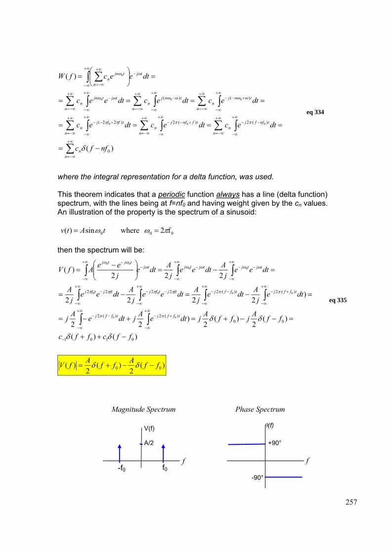
257
∑
∑ ∫∑ ∫∑ ∫
∑ ∫∑ ∫∑ ∫
∫ ∑
∞+
−∞=
∞+
−∞=
∞+
∞−
−−∞+
−∞=
∞+
∞−
+−−∞+
−∞=
∞+
∞−
+−−
∞+
−∞=
∞+
∞−
+−−∞+
−∞=
∞+
∞−
−∞+
−∞=
∞+
∞−
−
+∞
∞−
−+∞
−∞=
−=
====
====
=⎟⎠
⎞⎜⎝
⎛=
nn
n
tnffjn
n
tfnfjn
n
tffjn
n
tnjn
n
tnjn
n
tjtjnn
tj
n
tjnn
nffc
dtecdtecdtec
dtecdtecdteec
dteecfW
)(
)(
0
)(2)(2)22(
)()(
000
000
0
δ
ππππ
ωωωωωω
ωω
eq 334
where the integral representation for a delta function, was used. This theorem indicates that a periodic function always has a line (delta function) spectrum, with the lines being at f=nf0 and having weight given by the cn values. An illustration of the property is the spectrum of a sinusoid: f2 ere whsin)( 000 πωω == tAtv then the spectrum will be:
)()(
)(2
)(2
)22
)2222
222)(
0101
00)(2)(2
)(2)(22222
00
0000
0000
ffcffc
ffAjffAjdteAjdteAj
dtej
Adtej
Adteej
Adteej
A
dteej
Adteej
AdtejeeAfV
tffjtffj
tffjtffjftjtfjftjtfj
tjtjtjtjtjtjtj
−++
=−−+=+−=
=−=−=
=−=⎟⎟⎠
⎞⎜⎜⎝
⎛ −=
−
∞+
∞−
+−∞+
∞−
−−
∞+
∞−
+−∞+
∞−
−−−∞+
∞−
−−∞+
∞−
−+∞
∞−
−−+∞
∞−
−+∞
∞−
−
∫∫
∫∫∫∫
∫∫∫
δδ
δδππ
ππππππ
ωωωωωωω
eq 335
)(2
)(2
)( 00 ffAffAfV −−+= δδ
V(f)
A/2
f0 -f0
θ(f)
+90°
f
-90°
f
Magnitude Spectrum Phase Spectrum
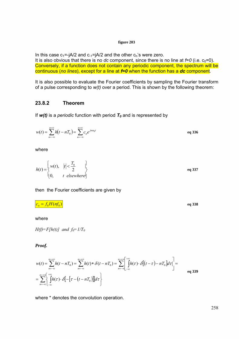
258
figure 203
In this case c1=-jA/2 and c-1=jA/2 and the other cn’s were zero. It is also obvious that there is no dc component, since there is no line at f=0 (i.e. c0=0). Conversely, if a function does not contain any periodic component, the spectrum will be continuous (no lines), except for a line at f=0 when the function has a dc component. It is also possible to evaluate the Fourier coefficients by sampling the Fourier transform of a pulse corresponding to w(t) over a period. This is shown by the following theorem:
23.8.2 Theorem If w(t) is a periodic function with period T0 and is represented by
( ) ∑∑∞=
−∞=
∞=
−∞=
=−=n
n
tjnn
n
necnTthtw 0
0)( ω eq 336
where
⎪⎭
⎪⎬⎫
⎪⎩
⎪⎨⎧ <
=elsewheret
Tttwth
,02
),()(
0
eq 337
then the Fourier coefficients are given by
)( 00 nfHfcn = eq 338
where H(f)=F[h(t)] and f0=1/T0 Proof.
( )[ ]
( )[ ][ ]∑ ∫
∑ ∫∑∑+∞=
−∞=
∞+
∞−
+∞=
−∞=
+∞
∞−
+∞=
−∞=
+∞=
−∞=
⎭⎬⎫
⎩⎨⎧
−−−⋅=
=⎥⎦
⎤⎢⎣
⎡−−⋅=−∗=−=
n
n
n
n
n
n
n
n
dnTth
dnTthnTtthnTthtw
ττδτ
ττδτδ
0
000
)(
)()()()()(
eq 339
where * denotes the convolution operation.
259
Thus,
∑∑+∞=
−∞=
+∞=
−∞=
−∗=−=n
n
n
n
nTtthnTthtw )()()()( 00 δ eq 340
But the impulse train may itself be represented by its Fourier series; that is,
∑∑+∞=
−∞=
+∞=
−∞=
=−n
n
tjnn
n
necnTt 0)( 0
ωδ eq 341
Where all the Fourier coefficients are just cn=f0. Substituting the last in the preceding equation we have:
∑∑∑∑+∞=
−∞=
+∞=
−∞=
+∞=
−∞=
+∞=
−∞=
∗=∗=−∗=−=n
n
tjnn
n
tjnn
n
n
n
n
efthecthnTtthnTthtw 00000 )()()()()()( ωωδ eq 342
Taking the Fourier transform of both sides we have
∑+∞=
−∞=
−=n
nnffffHfW )()()( 00δ eq 343
Using the preceding theorem ( ) [ ]∑+∞=
−∞=
=−=n
nn twFnffcfW )()( 0δ to compare the last
equation with we obtain
∑∑+∞=
−∞=
+∞=
−∞=
−=−=n
n
n
n
nffnfHfnffffHfW )()()()()( 00000 δδ eq 344
As an example we find the Fourier coefficients for the periodic rectangular wave shown below:
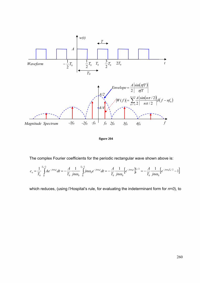
260
figure 204
The complex Fourier coefficients for the periodic rectangular wave shown above is:
[ ] [ ]11111 2/
00
2/0
00
2/
00
00
2/
00
0000
0
0
0
0 −−=−=−== −−−− ∫∫ TjnTtjnT
tjnT
tjnn e
jnTAe
jnTAdtejn
jnTAdtAe
Tc ωωωω
ωωω
ω
which reduces, (using l’Hospital’s rule, for evaluating the indeterminant form for n=0), to
w(t)
A
T0
T
021 T 0T 02
3 T 02T t 02
1 T−
f
A/2
A/4
f0 2f0 -2f0 3f0 -3f0 4f0 -f0
( )fT
fTAEnvelopeππsin
2=
( ) ( )∑+∞=
−∞=
−=n
n
nffn
nAfW 02/2/sin
2)( δ
ππ
Waveform
Magnitude Spectrum

261
[ ] [ ] [ ]
[ ] [ ] [ ]
( ) ( ) ( ) ( ) ( ) ( )
( ) ( ) ( ) ( ) ( ) ( )
( ) ( ) ( )
( ) ( ) ( ) ( ) ...........55
332
33
55
..........
...........5432
2345..........)(
5
03
01111111121
112112
112111
2
000
000
050403010
01020304050
5
4
3
00
2
00
2
00
2/2
002
0
0
0
0
2/2
0
0
2/
001
0
0000
0000
+−−−−−−−
−+−+−+=
+−+−+−+−++−
−−−−−−−−−−=−=
⇓
−=
=
−=
=−−=−−=⎥⎥⎦
⎤
⎢⎢⎣
⎡−−=−−=
−=−−−=−−=⎥⎥⎦
⎤
⎢⎢⎣
⎡−−=−−=
==
∑−∞=
−∞=
−−
−
−−
−
ffAjffAjffAjfA
ffAjffAjffAj
ffcffcffcffcfAfc
ffcffcffcffcffcnffcfW
Ajc
c
Ajc
jTAe
jTAe
jTAe
jTAc
Aj
TjT
Ae
TjT
Ae
TjT
AejT
Ac
termdcAc
n
nn
jT
Tj
Tj
jT
Tj
Tj
δπ
δπ
δπ
δ
δπ
δπ
δπ
δδδδδδ
δδδδδδ
π
π
ωωωω
ππππω
ππ
ω
ππ
ω
eq 345
These coefficients may be verified by using the last Theorem and the spectrum of the single flat-top impulse:
shaping) inpulsear (rectangul inpulse flat top a is
2t se 0,
2t se 1,
⎪⎭
⎪⎬
⎫
⎪⎩
⎪⎨
⎧
>
≤≡⎟⎟
⎠
⎞⎜⎜⎝
⎛=∏
s
s
ST
T
Tth(t)
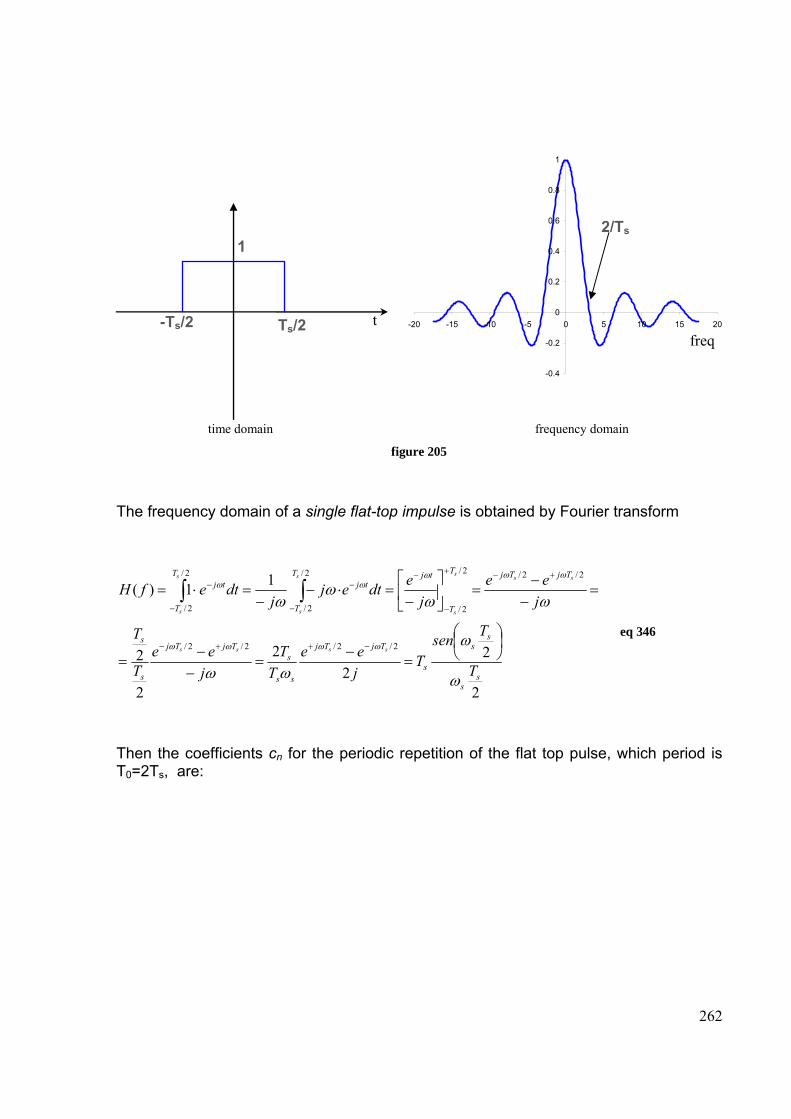
262
-0.4
-0.2
0
0.2
0.4
0.6
0.8
1
-20 -15 -10 -5 0 5 10 15 20
freq -Ts/2 Ts/2
1
t
2/Ts
time domain frequency domain
figure 205
The frequency domain of a single flat-top impulse is obtained by Fourier transform
2
22
2
2
2
11)(
2/2/2/2/
2/2/2/
2/
2/
2/
2/
2/
ss
ss
s
TjTj
ss
sTjTj
s
s
TjTjT
T
tjT
T
tjT
T
tj
T
TsenT
jee
TT
jee
T
T
jee
jedtej
jdtefH
ssss
sss
s
s
s
s
s
ω
ω
ωω
ωωω
ω
ωωωω
ωωωωω
⎟⎠⎞
⎜⎝⎛
=−
=−−
=
=−−
=⎥⎦
⎤⎢⎣
⎡−
=⋅−−
=⋅=
−++−
+−+
−
−
−
−
−
− ∫∫
eq 346
Then the coefficients cn for the periodic repetition of the flat top pulse, which period is T0=2Ts, are:
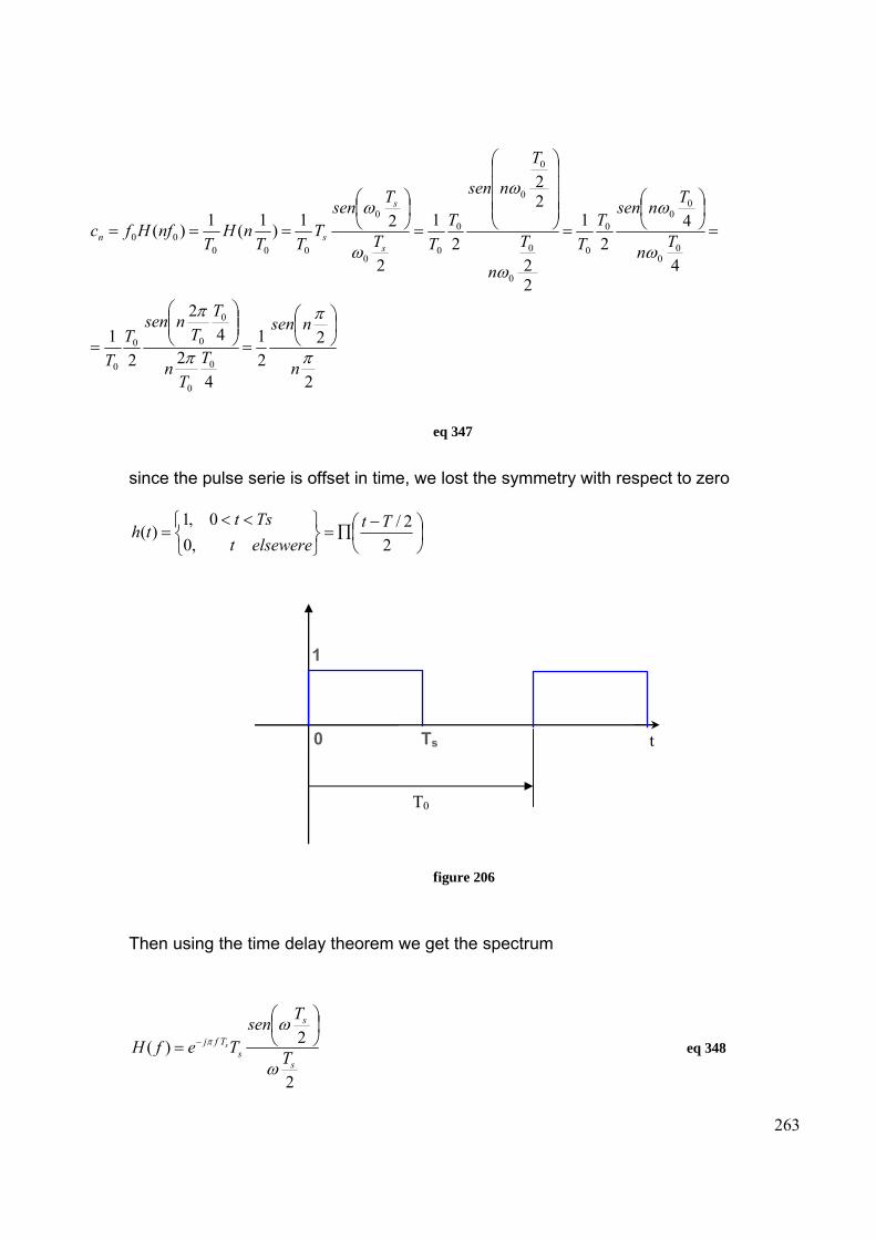
263
0 Ts
1
t
T0
2
221
42
42
21
4
42
1
22
22
21
2
21)1(1)(
0
0
0
00
0
00
00
0
00
0
0
0
0
00
0
00000
π
π
π
π
ω
ω
ω
ω
ω
ω
n
nsen
TT
n
TT
nsenT
T
Tn
TnsenT
TT
n
T
nsen
TTT
TsenT
TTnH
TnfHfc
s
s
sn
⎟⎠⎞
⎜⎝⎛
=⎟⎟⎠
⎞⎜⎜⎝
⎛
=
=⎟⎠⎞
⎜⎝⎛
=⎟⎟⎟⎟
⎠
⎞
⎜⎜⎜⎜
⎝
⎛
=⎟⎠⎞
⎜⎝⎛
===
eq 347
since the pulse serie is offset in time, we lost the symmetry with respect to zero
⎟⎠⎞
⎜⎝⎛ −
∏=⎭⎬⎫
⎩⎨⎧ <<
=2
2/,0
0,1)( Tt
elseweretTst
th
figure 206
Then using the time delay theorem we get the spectrum
2
2)(s
s
sTfj
T
TsenTefH s
ω
ωπ
⎟⎠⎞
⎜⎝⎛
= − eq 348

264
2
221
2
221
2
221 22
1 0
0
π
π
π
π
π
πππ
π
n
nsene
n
nsene
n
nsenec
jnT
Tjn
Tfjnn
s
⎟⎠⎞
⎜⎝⎛
=⎟⎠⎞
⎜⎝⎛
=⎟⎠⎞
⎜⎝⎛
=−−
− eq 349
which is identical to the preceding form of cn. The magnitude spectrum is illustrated by the solid lines on figure above. Since delta functions have infinite value, they can not be plotted; but the weights of the delta functions can be plotted as shown by the dashed line on figure. Now compare the spectrum for this periodic rectangular wave with the spectrum for the rectangular pulse alone. Note that the spectrum for the periodic wave contains spectral lines, whereas the spectrum for the non periodic pulse is continuous. Note that the envelope of the spectrum for both cases is the same [sin(x)/x] shape. Consequently, the null bandwidth (for the envelope) is 1/T for both cases, where T=Ts is the pulse with. This is a basic property of the digital signalling with rectangular pulse shapes: the null bandwidth is the reciprocal of the pulse with.
23.9 Guard Period For a given system bandwidth, the symbol rate for an OFDM signal is much lower than a single carrier transmission scheme. For example for a single carrier BPSK modulation, the symbol rate corresponds to the bit rate of the transmission. However for OFDM the system bandwidth is broken up into Nc subcarriers, resulting in a symbol rate that is Nc times lower than the single carrier transmission. This low symbol rate makes OFDM naturally resistant to effects of Inter-Symbol Interference (ISI) caused by multipath propagation. Multipath propagation is caused by the radio transmission signal reflecting off objects in the propagation environment, such as walls, buildings, mountains, etc. These multiple signals arrive at the receiver at different times due to the transmission distances being different. This spreads the symbol boundaries causing energy leakage between them. The effect of ISI on an OFDM signal can be further improved by the addition of a guard period to the start of each symbol. This guard period is a cyclic copy that extends the length of the symbol waveform. Each subcarrier, in the data section of the symbol, (i.e. the OFDM symbol with no guard period added, which is equal to the length of the IFFT size used to generate the signal) has an integer number of cycles. Because of this, placing copies of the symbol end-to-end results in a continuous signal, with no discontinuities at the joins. Thus by copying the end of a symbol and appending this to the start results in a longer symbol time. Figure below shows the insertion of a guard period.
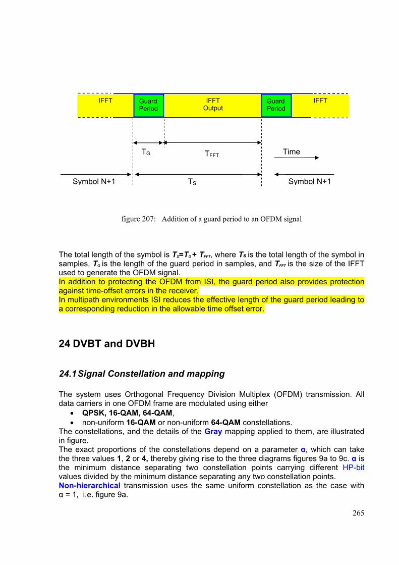
265
figure 207: Addition of a guard period to an OFDM signal
The total length of the symbol is TS=TG + TFFT, where Ts is the total length of the symbol in samples, TG is the length of the guard period in samples, and TFFT is the size of the IFFT used to generate the OFDM signal. In addition to protecting the OFDM from ISI, the guard period also provides protection against time-offset errors in the receiver. In multipath environments ISI reduces the effective length of the guard period leading to a corresponding reduction in the allowable time offset error.
24 DVBT and DVBH
24.1 Signal Constellation and mapping The system uses Orthogonal Frequency Division Multiplex (OFDM) transmission. All data carriers in one OFDM frame are modulated using either
• QPSK, 16-QAM, 64-QAM, • non-uniform 16-QAM or non-uniform 64-QAM constellations.
The constellations, and the details of the Gray mapping applied to them, are illustrated in figure. The exact proportions of the constellations depend on a parameter α, which can take the three values 1, 2 or 4, thereby giving rise to the three diagrams figures 9a to 9c. α is the minimum distance separating two constellation points carrying different HP-bit values divided by the minimum distance separating any two constellation points. Non-hierarchical transmission uses the same uniform constellation as the case with α = 1, i.e. figure 9a.
IFFT Guard Period
IFFT Output
Guard Period
IFFT
TFFTTG
TS
Time
Symbol N+1Symbol N+1
266
Re(z) y0,q’
Im(z) y1,q’ QPSK Bit ordering: y0,q’ y1,q’
QPSK Bit ordering: y0,q’ y1,q’
1-1
1
-1
00
01
10
11
267
25 Appendix
25.1 Convolution process The product convolution between two time functions is defined as:
( ) ( ) ( ) ( ) ( ) ( )[ ]∫∫+∞
∞−
+∞
∞−
−−∗=−∗=∗ ττττττ dtffdtfftftf 212121
As an example taking f1 and f2 as shown below and considering a shift τ=0 we have:
Inversion process
268
In the following example taking f1 and f2 as shown below and considering a shift τ=a we have:
f1(t)
t
f2(t)
t
Step 1: definizione delle funzioni
f1(τ)
τ
f2(t-τ)= f2[-(τ-t)]→ τ=0→ f2(t)= f2[-(-t)]
Step 2: inversione della f2 e shift temporale di τ=0
o
o o
o
f1(τ)
f2(t-τ)
Step 3: prodotto integrale da - ∞ a +∞ delle funzioni dello step 2
o o
τ
τ τ
Convoluzione di f1 con f2
269
f1(t)
t
f2(t)
t
Step 1: definizione delle funzioni
f1(τ)
τ
f2(t-τ)= f2[-(τ-t)]→ τ=a→ f2(t)= f2[-(a-t)]
Step 2: inversione della f2 e shift temporale di τ=a
o
o o
o
f1(τ)
f2(t-τ)
Step 3: prodotto integrale da - ∞ a +∞ delle funzioni dello step 2
o o
τ
τ τ
Convoluzione di f1 con f2
a
270
25.2 Dirac delta function and convolution process One property of Dirac delta function is that:
( ) ( ) ( ) ( ) ( )0000 111 fdtftf =−∗=∗ ∫+∞
∞−
τδδ
i.e.
( ) ( ) ( ) ( ) ( )tfdtfttf 111 =−∗=∗ ∫+∞
∞−
ττδτδ
If there is a shift T0 then:
( ) ( ) ( ) ( )[ ] ( )010101 TtfdTtfTttf −=−−∗=−∗ ∫+∞
∞−
ττδτδ
in this example τ=t-T0
271
26 Reference [1] 3GPP TS 05.04 V8.4.0 (2001) [ www.3gpp.org ] [2] Digital and Analog Communication System [Leon W.Couch 2001] [3] Implementation Effects on GSM,s EDGE Modulation [ Steven V.Schell, www.tropian.com]
E:\documenti per
corsi\ELETTRONICA T [4] WINIQ software for simulating EDGE signal [ www.rhode-swartz.com ] [5] Introduzione alla modulazioni numeriche [www.univpm Proff. Chiaraluce]
E:\documenti per corsi\ELETTRONICA T
[6] Digital modulation in a communications system [Hewlet Packard application note]
E:\documenti per corsi\EDGE_modulatio
[7] GMSK in nutshell [Thyerry Turletty 1996 Massachusetts Institute of Technology]
E:\documenti per
corsi\EDGE_modulatio [8] Digital modulation and GMSK [University of Hull] [9] Trasmissione delle informazioni [Proff. Diruscio] [10] Bandwidth efficient modulation [CCSDS 413.0-G-1 april 2003]
E:\documenti per corsi\telemeteryng en
[11] PROCEEDINGS OF THE CCSDS RF AND MODULATION SUBPANEL 1E MEETING OF MAY 2001 CONCERNING BANDWIDTH-EFFICIENT MODULATION [CCSDS 1999]
E:\documenti per corsi\telemeteryng en
[12] Theory of frequency and phase modulation [http://www.vk1od.net/FM/FM.htm#Frequency]
[13] http://telemetry.nmsu.edu/Conference_Pub.html
C:\documenti davide\documenti per corsi\E
[14] http://www.ee.byu.edu/faculty/mdr/publications.phtml [15] SFCG Meeting SF17 - 28/D Galveston, Texas 16-25 September 1997: CCSDS - SFCG
EFFICIENT MODULATION METHODS STUDY AT NASA/JPL PHASE 3: END-TO-END SYSTEM PERFORMANCE
C:\documenti davide\documenti per corsi\E
[16] OFDM_thesys_lawray [17] UMTS Architecture model vers 33 [Massaccesi Andrea]
Related Documents


![Dissertação Mestrado_Adriana Micheli[1].](https://static.cupdf.com/doc/110x72/587369641a28ab574d8bebef/dissertacao-mestradoadriana-micheli1.jpg)