North/Latin America http://aic.lgservice.com Europe/Africa http://eic.lgservice.com Asia/Oceania http://biz.lgservice.com Internal Use Only Printed in Korea P/NO : CHASSIS : MODEL : CAUTION BEFORE SERVICING THE CHASSIS, READ THE SAFETY PRECAUTIONS IN THIS MANUAL. SERVICE MANUAL MFL67237405 (1412-REV00) 49MS75A 49MS75A-5BB LW43B MONITOR SIGNAGE

Welcome message from author
This document is posted to help you gain knowledge. Please leave a comment to let me know what you think about it! Share it to your friends and learn new things together.
Transcript

North/Latin America http://aic.lgservice.comEurope/Africa http://eic.lgservice.comAsia/Oceania http://biz.lgservice.com
Internal Use Only
Printed in KoreaP/NO :
CHASSIS :
MODEL :
CAUTIONBEFORE SERVICING THE CHASSIS,READ THE SAFETY PRECAUTIONS IN THIS MANUAL.
SERVICE MANUAL
MFL67237405 (1412-REV00)
49MS75A 49MS75A-5BB
LW43B
MONITOR SIGNAGE

- 2 - LGE Internal Use OnlyCopyright © LG Electronics. Inc. All rights reserved.Only for training and service purposes
CONTENTS
CONTENTS .............................................................................................. 2
PRECAUTION ........................................................................................... 3
SERVICING PRECAUTIONS .................................................................... 4
SPECIFICATION ....................................................................................... 6
ADJUSTMENT INSTRUCTION ................................................................ 8
BLOCK DIAGRAM .................................................................................. 15
EXPLODED VIEW .................................................................................. 16
SCHEMATIC CIRCUIT DIAGRAM ........................................... APPENDIX
TROUBLE SHOOTING GUIDE ................................................ APPENDIX

- 3 - LGE Internal Use OnlyCopyright © LG Electronics. Inc. All rights reserved.Only for training and service purposes
WARNING FOR THE SAFETY-RELATED COMPONENT.
• There are some special components used in LCD monitor that are important for safety. These parts are marked on the schematic diagram and the Exploded View. It is essential that these critical parts should be replaced with the manufacturer' s specified parts to prevent electric shock, fire or other hazard.
• Do not modify original design without obtaining written permission from manufacturer or you will void the original parts and labor guarantee.
TAKE CARE DURING HANDLING THE LCD MODULE WITH BACKLIGHT UNIT.
• Must mount the module using mounting holes arranged in four corners.
• Do not press on the panel, edge of the frame strongly or electric shock as this will result in damage to the screen.
• Do not scratch or press on the panel with any sharp objects, such as pencil or pen as this may result in damage to the panel.
• Protect the module from the ESD as it may damage the electronic circuit (C-MOS).
• Make certain that treatment person' s body are grounded through wrist band.
• Do not leave the module in high temperature and in areas of high humidity for a long time.
• The module not be exposed to the direct sunlight.
• Avoid contact with water as it may a short circuit within the module.
• If the surface of panel become dirty, please wipe it off with a softmaterial. (Cleaning with a dirty or rough cloth may damage the panel.)
WARNINGBE CAREFUL ELECTRIC SHOCK !
• If you want to replace with the new backlight or inverter circuit, must disconnect the AC adapter because high voltage appears at inverter circuit about 650Vrms.
• Handle with care wires or connectors of the inverter circuit. If the wires are pressed cause short and may burn or take fire.
Leakage Current Hot Check Circuit
• Replaceable batteries CAUTION
RISK OF EXPLOSION IF BATTERY IS REPLACED BY AN INCORRECT TYPE. DISPOSE OF USED BATTERIES ACCORDING TO THE INSTRUCTIONS. REPLACE ONLY WITH THE SAME OR EQUIVALENT TYPE.
PRECAUTION
1.5 Kohm/10W
0.15µFTo Instrument'sexposed METALLIC PARTS
Good Earth Groundsuch as WATER PIPE,CONDUIT etc.
AC Volt-meter
When 25A is impressed between Earth and 2nd Groundfor 1 second, Resistance must be less than 0.1*Base on Adjustment standard
CAUTIONPlease use only a plastic screwdriver to protect yourself from shock hazard during service operation.
ADVARSELLithiumbatteri - Eksplosionsfare ved fejlagtighåndtering.Udskiftning må kun ske med batteri af sammefabrikat og type.Levér det brugte batteri tilbage til leverandøren.

- 4 - LGE Internal Use OnlyCopyright © LG Electronics. Inc. All rights reserved.Only for training and service purposes
CAUTION: Before servicing receivers covered by this service manual and its supplements and addenda, read and follow the SAFETY PRECAUTIONS on page 3 of this publication.NOTE: If unforeseen circumstances create conflict between the following servicing precautions and any of the safety precautions on page 3 of this publication, always follow the safety precautions. Remember: Safety First.
General Servicing Precautions1. Always unplug the receiver AC power cord from the AC power
source before;a. Removing or reinstalling any component, circuit board
module or any other receiver assembly.b. Disconnecting or reconnecting any receiver electrical plug or
other electrical connection.c. Connecting a test substitute in parallel with an electrolytic
capacitor in the receiver. CAUTION: A wrong part substitution or incorrect polarity
installation of electrolytic capacitors may result in an explosion hazard.
2. Test high voltage only by measuring it with an appropriate high voltage meter or other voltage measuring device (DVM, FETVOM, etc) equipped with a suitable high voltage probe.
Do not test high voltage by "drawing an arc".3. Do not spray chemicals on or near this receiver or any of its
assemblies.4. Unless specified otherwise in this service manual, clean
electrical contacts only by applying the following mixture to the contacts with a pipe cleaner, cotton-tipped stick or comparable non-abrasive applicator; 10% (by volume) Acetone and 90% (by volume) isopropyl alcohol (90%-99% strength)
CAUTION: This is a flammable mixture. Unless specified otherwise in this service manual, lubrication of
contacts in not required.5. Do not defeat any plug/socket B+ voltage interlocks with which
receivers covered by this service manual might be equipped.6. Do not apply AC power to this instrument and/or any of its
electrical assemblies unless all solid-state device heat sinks are correctly installed.
7. Always connect the test receiver ground lead to the receiver chassis ground before connecting the test receiver positive lead.
Always remove the test receiver ground lead last.8. Use with this receiver only the test fixtures specified in this
service manual. CAUTION: Do not connect the test fixture ground strap to any
heat sink in this receiver.
Electrostatically Sensitive (ES) DevicesSome semiconductor (solid-state) devices can be damaged easily by static electricity. Such components commonly are called Electrostatically Sensitive (ES) Devices. Examples of typical ES devices are integrated circuits and some field-effect transistors and semiconductor "chip" components. The following techniques should be used to help reduce the incidence of component damage caused by static by static electricity.1. Immediately before handling any semiconductor component or
semiconductor-equipped assembly, drain off any electrostatic charge on your body by touching a known earth ground. Alternatively, obtain and wear a commercially available discharging wrist strap device, which should be removed to prevent potential shock reasons prior to applying power to the
unit under test.2. After removing an electrical assembly equipped with ES
devices, place the assembly on a conductive surface such as aluminum foil, to prevent electrostatic charge buildup or exposure of the assembly.
3. Use only a grounded-tip soldering iron to solder or unsolder ES devices.
4. Use only an anti-static type solder removal device. Some solder removal devices not classified as "anti-static" can generate electrical charges sufficient to damage ES devices.
5. Do not use freon-propelled chemicals. These can generate electrical charges sufficient to damage ES devices.
6. Do not remove a replacement ES device from its protective package until immediately before you are ready to install it. (Most replacement ES devices are packaged with leads electrically shorted together by conductive foam, aluminum foil or comparable conductive material).
7. Immediately before removing the protective material from the leads of a replacement ES device, touch the protective material to the chassis or circuit assembly into which the device will be installed.
CAUTION: Be sure no power is applied to the chassis or circuit, and observe all other safety precautions.
8. Minimize bodily motions when handling unpackaged replacement ES devices. (Otherwise harmless motion such as the brushing together of your clothes fabric or the lifting of your foot from a carpeted floor can generate static electricity sufficient to damage an ES device.)
General Soldering Guidelines1. Use a grounded-tip, low-wattage soldering iron and appropriate
tip size and shape that will maintain tip temperature within the range or 500 ˚F to 600 ˚F.
2. Use an appropriate gauge of RMA resin-core solder composed of 60 parts tin/40 parts lead.
3. Keep the soldering iron tip clean and well tinned.4. Thoroughly clean the surfaces to be soldered. Use a mall wire-
bristle (0.5 inch, or 1.25cm) brush with a metal handle. Do not use freon-propelled spray-on cleaners.5. Use the following unsoldering technique
a. Allow the soldering iron tip to reach normal temperature. (500 ˚F to 600 ˚F)b. Heat the component lead until the solder melts.c. Quickly draw the melted solder with an anti-static, suction-
type solder removal device or with solder braid. CAUTION: Work quickly to avoid overheating the circuit
board printed foil.6. Use the following soldering technique.
a. Allow the soldering iron tip to reach a normal temperature (500 ˚F to 600 ˚F)
b. First, hold the soldering iron tip and solder the strand against the component lead until the solder melts.
c. Quickly move the soldering iron tip to the junction of the component lead and the printed circuit foil, and hold it there only until the solder flows onto and around both the component lead and the foil.
CAUTION: Work quickly to avoid overheating the circuit board printed foil.
d. Closely inspect the solder area and remove any excess or splashed solder with a small wire-bristle brush.
SERVICING PRECAUTIONS

- 5 - LGE Internal Use OnlyCopyright © LG Electronics. Inc. All rights reserved.Only for training and service purposes
IC Remove/ReplacementSome chassis circuit boards have slotted holes (oblong) through which the IC leads are inserted and then bent flat against the circuit foil. When holes are the slotted type, the following technique should be used to remove and replace the IC. When working with boards using the familiar round hole, use the standard technique as outlined in paragraphs 5 and 6 above.
Removal1. Desolder and straighten each IC lead in one operation by gently
prying up on the lead with the soldering iron tip as the solder melts.
2. Draw away the melted solder with an anti-static suction-type solder removal device (or with solder braid) before removing the IC.
Replacement1. Carefully insert the replacement IC in the circuit board.2. Carefully bend each IC lead against the circuit foil pad and
solder it.3. Clean the soldered areas with a small wire-bristle brush. (It is not necessary to reapply acrylic coating to the areas).
"Small-Signal" Discrete TransistorRemoval/Replacement1. Remove the defective transistor by clipping its leads as close as
possible to the component body.2. Bend into a "U" shape the end of each of three leads remaining
on the circuit board.3. Bend into a "U" shape the replacement transistor leads.4. Connect the replacement transistor leads to the corresponding
leads extending from the circuit board and crimp the "U" with long nose pliers to insure metal to metal contact then solder each connection.
Power Output, Transistor DeviceRemoval/Replacement1. Heat and remove all solder from around the transistor leads.2. Remove the heat sink mounting screw (if so equipped).3. Carefully remove the transistor from the heat sink of the circuit
board.4. Insert new transistor in the circuit board.5. Solder each transistor lead, and clip off excess lead.6. Replace heat sink.
Diode Removal/Replacement1. Remove defective diode by clipping its leads as close as
possible to diode body.2. Bend the two remaining leads perpendicular y to the circuit
board.3. Observing diode polarity, wrap each lead of the new diode
around the corresponding lead on the circuit board.4. Securely crimp each connection and solder it.5. Inspect (on the circuit board copper side) the solder joints of
the two "original" leads. If they are not shiny, reheat them and if necessary, apply additional solder.
Fuse and Conventional ResistorRemoval/Replacement1. Clip each fuse or resistor lead at top of the circuit board hollow
stake.2. Securely crimp the leads of replacement component around
notch at stake top.3. Solder the connections.
CAUTION: Maintain original spacing between the replaced component and adjacent components and the circuit board to prevent excessive component temperatures.
Circuit Board Foil RepairExcessive heat applied to the copper foil of any printed circuit board will weaken the adhesive that bonds the foil to the circuit board causing the foil to separate from or "lift-off" the board. The following guidelines and procedures should be followed whenever this condition is encountered.
At IC ConnectionsTo repair a defective copper pattern at IC connections use the following procedure to install a jumper wire on the copper pattern side of the circuit board. (Use this technique only on IC connections).
1. Carefully remove the damaged copper pattern with a sharp knife. (Remove only as much copper as absolutely necessary).
2. carefully scratch away the solder resist and acrylic coating (if used) from the end of the remaining copper pattern.
3. Bend a small "U" in one end of a small gauge jumper wire and carefully crimp it around the IC pin. Solder the IC connection.
4. Route the jumper wire along the path of the out-away copper pattern and let it overlap the previously scraped end of the good copper pattern. Solder the overlapped area and clip off any excess jumper wire.
At Other ConnectionsUse the following technique to repair the defective copper pattern at connections other than IC Pins. This technique involves the installation of a jumper wire on the component side of the circuit board.
1. Remove the defective copper pattern with a sharp knife. Remove at least 1/4 inch of copper, to ensure that a hazardous
condition will not exist if the jumper wire opens.2. Trace along the copper pattern from both sides of the pattern
break and locate the nearest component that is directly connected to the affected copper pattern.
3. Connect insulated 20-gauge jumper wire from the lead of the nearest component on one side of the pattern break to the lead of the nearest component on the other side.
Carefully crimp and solder the connections. CAUTION: Be sure the insulated jumper wire is dressed so the
it does not touch components or sharp edges.

- 6 - LGE Internal Use OnlyCopyright © LG Electronics. Inc. All rights reserved.Only for training and service purposes
SPECIFICATION1. Application range
This specification is applied to the LW43B chassis.
2. Requirement for TestEach part is tested as below without special appointment.
1) Temperature: 25 °C ± 5 °C(77 °F ± 9 °F), CST: 40 °C ± 5 °C2) Relative Humidity: 65 % ± 10 %3) Power Voltage : Standard input voltage (AC 100 - 240 V~, 50 / 60 Hz)* Standard Voltage of each products is marked by models.4) Specification and performance of each parts are followed
each drawing and specification by part number in accord-ance with BOM.
5) The receiver must be operated for about 5 minutes prior to the adjustment.
3. Test method1) Performance: LGE Monitor test method followed. 2) Demanded other specification - Safety : CE, IEC specification- EMC : CE, IEC
4. General Specification
No. Item Content Remark
1 HDMI Input (2EA) HDMI Rear / support D-TV&PC resolution
2 DVI Input (1EA) DVI
3 DP Input(1EA)/Output(1EA) DP Rear / support D-TV&PC resolution
4 Audio Input (1EA) DVI Audio L/R Input
5 OPS Input(1EA) OPS(Open Pluggable Specification: Built-in PC) Optional Docking Port(OPS Kit Accessory)
6 Speaker Output (1EA) Compatible with common speaker 10W*2Ch Output
7 IR&Brightness Sensor Input (1EA)
IR&Brightness Sensor
8 Pixel Sensor Input (1EA) Pixel Sensor Optional
9 External USB (1EA) Picture, Music, Movie, SVC Device : Memory Stick, Mouse, Keyboard, Wi-Fi USB Dongle
10 RS-232C Input(1EA)/Out-put (1EA)
Display Control
11 LAN(1EA) RJ45, 100BASE-T Network Connection for SuperSign-W/SuperSign-C
12 Local Key 8 keys
4.1. General Specification
No. Item Specification Remarks1 Supported Sync. Type Digital
2 Operating Frequency DigitalHorizontal 30 - 83 kHzVertical 60 Hz Only
3 Resolution DigitalMax 1920 × 1080 @ 60 HzRecommend 1920 × 1080 @ 60 Hz
4.2. DVI-D, HDMI, Display Port (PC) Specification

- 7 - LGE Internal Use OnlyCopyright © LG Electronics. Inc. All rights reserved.Only for training and service purposes
No. Section Pol. Dot Clock[MHz]
Frequency[kHz]/[Hz]
Total Cycle
(E)
Display(A)
FrontPorch(B)
Sync.(D)
BackPorch(F)
Resolution
1 H(Pixels) - 25.175 31.469 800 640 16 96 48 640 x 480
V(Lines) - 59.94 525 480 10 2 33
2 H(Pixels) + 40.0 37.879 1056 800 40 128 88 800 x 600
V(Lines) + 60.317 628 600 1 4 23
3 H(Pixels) - 65.0 48.363 1344 1024 24 136 160 1024 x 768
V(Lines) - 60.0 806 768 3 6 29
4 H(Pixels) + 74.5 44.772 1664 1280 64 128 192 1280 x 720
V(Lines) + 59.855 748 720 3 5 20
5 H(Pixels) - 85.86 47.7 1800 1366 72 144 216 1366 x 768
V(Lines) - 60 795 768 1 3 23
6 H(Pixels) + 108.0 63.981 1688 1280 48 112 248 1280 x 1024
V(Lines) + 60.02 1066 1024 1 3 38
7 H(Pixels) - 146.25 65.290 2240 1680 104 176 280 1680 x 1050
V(Lines) + 59.954 1089 1050 3 6 30
8 H(Pixels) + 148.5 67.5 2200 1920 88 44 88 1920 x 1080
V(Lines) + 60 1125 1080 4 5 46
5. Signal Timing (Supporting Resolution)5.1. DVI, HDMI, Display Port (PC Mode )
5.2. HDMI, DisplayPort (DTV Mode ) * DVI Input dont support DTV Mode
No.Specification Remark
Resolution H-freq(kHz) V-freq(Hz) Proposed
1 480/60P 31.5 60 EDTV 480p
2 576/50P 31.25 50 EDTV 576p
3 720/50P 37.5 50 HDTV 720p
4 720/60P 45 60 HDTV 720p
5 1080/50i 28.1 50 HDTV 1080i 50Hz For Australian
6 1080/60i 33.75 60 HDTV 1080i 60Hz
7 1080/50P 56.25 50 HDTV 1080P 50Hz
8 1080/60P 67.5 60 HDTV 1080P 60Hz

- 8 - LGE Internal Use OnlyCopyright © LG Electronics. Inc. All rights reserved.Only for training and service purposes
ADJUSTMENT INSTRUCTION1. Application Range
This spec sheet is applied all of the Digital Signage Product with LW43B chassis.
2. Specification1) Because this is not a hot chassis, it is not necessary to
use an isolation transformer. However, the use of isolation transformer will help protect test instrument.
2) Adjustment must be done in the correct order. 3) The adjustment must be performed in the circumstance of
25 °C ± 5 °C of temperature and 65 % ± 10 % of relative humidity if there is no specific designation.
4) The input voltage of the receiver must keep AC 100-240 V~, 50/60 Hz.
5) At first Worker must turn on the SET by using Power Only key.
6) The receiver must be operated for about 5 minutes prior to the adjustment when module is in the circumstance of over 15.
In case of keeping module is in the circumstance of 0 °C, it should be placed in the circumstance of above 15 °C for 2 hours.
In case of keeping module is in the circumstance of below -20 °C, it should be placed in the circumstance of above 15 °C for 3 hours.
Caution) When still image is displayed for a period of 20 min-utes or longer (especially where W/B scale is strong. Digital pattern 13ch and/or Cross hatch pattern 09ch), there can some afterimage in the black level area
3. Adjustment items3.1. Main PCBA Adjustments MAC Address
Download 1) ADC adjustment: Digital Only [does not apply]2) EDID / DDC Download.3) MAC Address Download * Remark - Above adjustment items can be also performed in
Final Assembly if needed. Adjustment items in both PCBA and final assembly stages can be checked by using the INSTART Menu → ADJUST CHECK.
3.2. Final Assembly adjustment1) White Balance adjustment2) RS-232C functionality check3) Factory Option setting per destination4) Shipment mode setting (IN-STOP)5) GND and HI-POT test
3.3. Appendix.1) Ship-out mode2) Service Option Default3) Tool option menu, USB Download (S/W Update, Option,
service only)4) ISP Download (Optional)
4. MAIN PCBA Adjustments4.1. ADC Calibration [MS75A Model Digital
Only Model: does not apply] - An ADC calibration is not necessary because MAIN
SoC (LGExxxx) is already calibrated from IC Maker - If it needs to adjust manually, refer to appendix.
4.2. MAC Address4.2.1. Equipment & Condition
1) Play file: keydownload.exe
4.2.2. Communication Port connection1) Key Write: Com 1,2,3,4 and 115200 (Baudrate)2) Barcode: Com 1,2,3,4 and 9600 (Baudrate)
4.2.3. Download process1) Select the download items.2) Mode check: Online Only3) Check the test process : DETECT → MAC_WRITE 4) Play: START5) Check of result: Ready, Test, OK or NG
4.2.4. Communication Port connection1) Connect : PCBA Jig → RS-232C Port == PC → RS-232C
Port
4.2.5. Download

- 9 - LGE Internal Use OnlyCopyright © LG Electronics. Inc. All rights reserved.Only for training and service purposes
4.3. LAN Inspection4.3.1. Equipment & Condition
Each other connection to LAN Port of IP Hub and Jig
4.3.2. LAN inspection solution1) LAN Port connection with PCB2) Network setting at MENU Mode of SET (Installer Menu →
119 → 253 → Menu)3) Setting automatic IP4) Setting state confirmation→ If automatic setting is finished, you confirm IP and MAC
Address.
4.4. LAN PORT INSPECTION(PING TEST)4.4.1. Equipment setting
1) Play the LAN Port Test PROGRAM.2) Input IP set up for an inspection to Test Program.*IP Number : 12.12.2.2
4.4.2. LAN PORT inspection(PING TEST)1) Play the LAN Port Test Program.2) Connect each other LAN Port Jack.3) Play Test (F9) button and confirm OK Message.4) Remove LAN cable.
4.5 Serial number downloadConnect Bar Code scan equipment and set by RS-232C cable.1) E2PROM Data Write
2) E2PROM Data Read
4.6 EDID/DDC Download (EDID PCM)4.6.1 Overview
It is a VESA regulation. A PC or a MNT will display an optimal resolution through information sharing without any necessity of user input. It is a realization of “Plug and Play”.
4.6.2 Equipment1) Since EDID data is embedded, EDID download JIG, HDMI
cable and D-sub are not need.2) Adjust by using remote controller.
4.6.3 Download method1) Press Adj. key on the Adj. R/C,2) Select EDID D/L (PCM) menu.3) By pressing Enter key, EDID download will begin4) If Download is successful, OK is display, but If Download is
failure, NG is displayed.5) If Download is failure, Re-try downloads.
→ Caution) When EDID Download, must remove HDMI / D-sub Cable.
4.6.4. EDID DATA1) DVI (Check Sum : 0x3C)

- 10 - LGE Internal Use OnlyCopyright © LG Electronics. Inc. All rights reserved.Only for training and service purposes
2) HDMI 1 (Check Sum : 0x3E, 0xA2)
3) HDMI 2 (Check Sum : 0x3E, 0x92)
4) DP (Check Sum : 0x3C, 0xA2)
5) OPS (Check Sum : 0x3E, 0x82)
5. Final Assembly Adjustment5.1. White Balance Adjustment5.1.1. Overview5.1.1.1. W/B adj. Objective & How-it-works
1) Objective: To reduce each Panel's W/B deviation2) How-it-works : When R/G/B gain in the OSD is at 192, it
means the panel is at its Full Dynamic Range. In order to prevent saturation of Full Dynamic range and data, one of R/G/B is fixed at 192, and the other two is lowered to find the desired value.
3) Adjustment condition : normal temperature - Surrounding Temperature : 25 °C ± 5 °C - Warm-up time: About 5 Min - Surrounding Humidity : 20 % ~ 80 % - Before White balance adjustment, Keep power on
status, don’t power off5.1.1.2. Adj. condition and cautionary items
1) Lighting condition in surrounding area surrounding lighting should be lower 10 lux. Try to isolate adj. area into dark surrounding.
2) Probe location: Color Analyzer (CA-210) probe should be within 10cm and perpendicular of the module surface (80°~ 100°)
3) Aging time - After Aging Start, Keep the Power ON status during 5
Minutes. - In case of LCD, Back-light on should be checked us-
ing no signal or Full-white pattern.
5.1.2. Equipment1) Color Analyzer: CA-210 (NCG: CH 9 / WCG: CH12 / LED:
CH14)2) Adj. Computer(During auto adj., RS-232C protocol is
needed)3) Adjust Remocon4) Video Signal Generator MSPG-925F 720p/204-
Gray(Model:217, Pattern:49)* Only when internal pattern is not available* Color Analyzer Matrix should be calibrated using CS-1000.
5.1.3. Equipment connection MAP
Color Analyzer
Computer
Pattern Generator※
※If Signage internal pattern is used, not needed
Signal Source
Probe
RS-232C
RS-232C
RS-232C

- 11 - LGE Internal Use OnlyCopyright © LG Electronics. Inc. All rights reserved.Only for training and service purposes
5.1.4. Adj. Command (Protocol) RS-232C Command used during auto-adjustment.
Ex) wb 00 00 -> Begin white balance auto-adj. wb 00 10 -> Gain adj. ja 00 ff -> Adj. data jb 00 c0 ... ... wb 00 1f → Gain adj. completed*(wb 00 20(Start), wb 00 2f(end)) → Off-set adj. wb 00 ff → End white balance auto-adj.
Adj. Map
5.1.5. Adj. method5.1.5.1 Auto WB calibration
1) Set in ADJ mode using P-ONLY key (or POWER ON key)2) Place optical probe on the center of the display - It need to check probe condition of zero calibration
before adjustment.3) Connect RS-232C Cable4) Select mode in ADJ Program and begin a adjustment.5) When WB adjustment is completed with OK message,
check adjustment status of pre-set mode (Cool, Medium, Warm)
6) Remove probe and RS-232C cable. W/B Adj. must begin as start command “wb 00 00” ,
and finish as end command “wb 00 ff”, and Adj. offset if need
5.1.5.2 Manual adjustment Method.1) Set in Adj. mode using POWER ON 2) Zero Calibrate the probe of Color Analyzer, then place it on
the center of LCD module within 10cm of the surface.. 3) Press ADJ key → EZ adjust using adj. R/C → White-
Balance then press the cursor to the right (KEY). When KEY () is pressed 204 Gray (80IRE) internal patterns will be displayed.
4) Adjust Cool modes - Fix the one of R/G/B gain to 192 (default data) and
decrease the others. ( If G gain is adjusted over 172 and R and B gain less than 192 , Adjust is O.K.)
- If G gain is less than 172, Increase G gain by up to 172, and then increase R gain and G gain same amount of increasing G gain.
- If R gain or B gain is over 255, Readjust G gain less than 172, Conform to R gain is 255 or B gain is 255
5) Adj. is performed in COOL, MEDIUM, WARM 3 modes of color temperature.
6) Adj. is completed, Exit adjust mode using “EXIT” key on Remote controller.
If internal pattern is not available, use RF input. In EZ Adj. menu 6.White Balance, you can select one of 2 Test-pattern : ON, OFF. Default is inner (ON). By selecting OFF, you can adjust using RF signal in 206 Gray pattern.
5.1.5.3 Adj. condition and cautionary items1) Lighting condition in surrounding area Surrounding lighting
should be lower 10 lux. Try to isolate adj. area into dark surrounding.
2) Probe location: CA-210 probe should be within 10cm and perpendicular of the module surface (80°~ 100°)
3) Aging time - After Aging Start, Keep the Power ON status during 5
Minutes. - In case of LCD, Back-light on should be checked us-
ing no signal or Full-white pattern.
5.1.6. Reference (White balance Adj. coordinate and color temperature)
Luminance : 204 Gray (80IRE) Standard color coordinate and temperature using CA-210 (CH14) : [applied only LGD Module]
Standard color coordinate and temperature using CA-210(CH 14) – by aging time
1) Egde LED models (applied only LGD Module) in LGEKR (GUMI) And LGERS
RS-232C COMMAND[CMD ID DATA] Explantion
wb 00 00 Begin White Balance adjustment
wb 00 ff End White Balance adjustment(internal pattern disappears )
Adj. item Command(lower caseASCII)
Data Range(Hex.)
Default(Decimal)
CMD1 CMD2 MIN MAX
Cool
R Gain j G 00 C0G Gain j H 00 C0B Gain j I 00 C0R CutG CutB Cut
Medium
R Gain j A 00 C0G Gain j B 00 C0B Gain j C 00 C0R CutG CutB Cut
Warm
R Gain j D 00 C0G Gain j E 00 C0B Gain j F 00 C0R CutG CutB Cut Mode
CoordinateTemp ∆uv
x yCool 0.271±0.002 0.270±0.002 13,000K -0.003
Medium 0.286±0.002 0.289±0.002 9,300K 0.0000 Warm 0.313±0.002 0.329±0.002 6,500K 0.0000
NetCast3.0
Aging time(Min)
Cool Medium WarmX y x y x y
271 270 286 289 313 3291 0-2 276 278 291 297 318 3372 3-5 275 276 290 295 317 3353 6-9 274 275 289 294 316 3344 10-19 273 274 288 293 315 3335 20-35 272 273 287 292 314 3326 36-49 272 272 287 291 314 3317 50-79 271 271 286 290 313 3308 80-119 271 270 286 289 313 3299 Over 120 271 270 286 289 313 329

- 12 - LGE Internal Use OnlyCopyright © LG Electronics. Inc. All rights reserved.Only for training and service purposes
2) Egde Direct LED models (applied only LGD Module) in LGEKR (GUMI for Winter Season)
Standard color coordinate and temperature using CA-210(CH-14) – by aging time
5.2. Ship-out mode check (In-stop) After final inspection, press In-Stop key of the Adj. R/C and check that the unit goes to Stand-by mode
6. Audio6.1. Audio input condition
1) Only DVI PC Input
6.2. Specification
7. GND and HI-POT Test
7.1. GND & HI-POT auto-check preparation1) Check the POWER CABLE and SIGNAL CABE insertion
condition
7.2. GND & HI-POT auto-check1) Pallet moves in the station. (POWER CORD / AV CORD is
tightly inserted)2) Connect the AV JACK Tester.3) Controller (GWS103-4) on.4) GND Test (Auto) - If Test is failed, Buzzer operates. - If Test is passed, execute next process (Hi-pot test).
Remove A/V CORD from A/V JACK BOX)
5) HI-POT test (Auto) - If Test is failed, Buzzer operates. - If Test is passed, GOOD Lamp on and move to next
process automatically.
7.3. Checkpoint1) Test voltage - GND: 1.5KV/min at 100mA - SIGNAL: 3KV/min at 100mA2) TEST time: 1 second3) TEST POINT - GND Test = POWER CORD GND and SIGNAL CA-
BLE GND. - Hi-pot Test = POWER CORD GND and LIVE & NEU-
TRAL.4) LEAKAGE CURRENT: At 0.5mArms
8. EYE Q Green Inspection8.1 Method
1) Connect the Power and IR+Brightness Sensor cable to the set.
2) Turn on the Signage SET.3) Press “P-Only→ Exit → EYE” Button on the adjustment of
R/C.
4) Green Eye-Check Box on the screen after 3 seconds.5) Cover the IR+Brightness Cable Assy with your hands, hold
it for 3 second6) If normal operation is indicated the "OK " on the screen7) If the "NG ", replace the IR+Brightness Cable Assy or Sen-
sor.8) Please test again after changing the cable.9) Please Press the In-Stop Button after completing the test.
[Note] Check the sensor data on the screen, make certain that data is below 20. If data isn’t below 20 in 3 seconds, EYE Q sensor would be bad. You should change EYE Q sen-sor.
8.2 Pixel Sensor Inspection Manual* Pixel Sensor Kit Parts
- SET / Power Cord / IR+Brightness Cable Assy / Remote Control
No. Item Min Typ Max Unit Remark
1.
Audio practical max Output, L/R(Distortion=10% max Output)
9.0 10.0 12.0 WMeasurement conditionEQ OffAVL OffClear Voice Off
8.5 8.9 9.8 Vrms
2. Speaker (8ΩImpedance) 10.0 14.0 W
NetCast3.0
Aging time(Min)
Cool Medium WarmX y x y x y
271 270 286 289 313 3291 0-2 280 282 295 301 322 3412 3-5 279 281 294 300 321 3403 6-9 278 280 293 299 320 3394 10-19 277 279 292 298 319 3385 20-35 276 277 291 296 318 3366 36-49 274 275 289 294 316 3347 50-79 273 273 288 292 315 3328 80-119 272 271 287 290 314 3209 Over 120 271 270 286 289 313 329

- 13 - LGE Internal Use OnlyCopyright © LG Electronics. Inc. All rights reserved.Only for training and service purposes
* Method1) Connect the cable Assy[Power Cord] on the set.
2) Connect the cable Assy[IR+Brightness Cable] on the set.
3) Connect the cable Assy[Pixel Sensor Cable] on the set.
4) Turn on the Signage SET.
5) As follows: the remote control operation.
a. Press " P-ONLY " on the adjustment of R/C.
b. Press " EXIT " on the adjustment of R/C.
c. Press “EYE Button” on the adjustment of R/C- Please Check the R,G,B pattern on the Screen.
- Check the sensor data on the screen- Please check RGB Sensor-Check On the screen. OK : Pass . NG : Fail [Re-Run]
Power Cord Connection
IR+Brigntness Cable Connection
Pixel Sensor Cable Connection
1
2
3
a
b
c

- 14 - LGE Internal Use OnlyCopyright © LG Electronics. Inc. All rights reserved.Only for training and service purposes
9. USB S/W Download(Service only)1) Put the USB Stick to the USB socket 2) Automatically detecting update file in USB Stick - If your downloaded program version in USB Stick is
lower than that of Signage set, it didn’t work. Other-wise USB data is automatically detected.
3) Updating is staring.
4) Updating Completed, The Signage will restart automatically5) If your Signage is turned on, check your updated version
and Tool option.(explain the Tool option, next stage) * If downloading version is more high than your Signage
have, Signage can lost all channel data. In this case, you have to channel recover. If all channel data is cleared, you didn’t have a DTV/ATV test on production line.
* After downloading, have to adjust Tool Option again.1) Push "IN-START" key in service remote control.2) Select "Tool Option 1" and push "OK" key.3) Punch in the number. (Each model has their number)
10. Optional adjustments10.1. Manual ADC Calibration10.1.1. Equipment & Condition
1) Adjustment Remocon2) 801GF (802B, 802F, 802R) or MSPG925FA Pattern Gen-
erator - Resolution: 480i Comp1 (MSPG-925FA: model-209,
pattern-65) - Resolution: 1080p Comp1 (MSPG-925FA: model-225,
pattern-65) - Resolution : 1080p RGB (MSPG-925FA: model-225,
pattern-65) - Pattern: Horizontal 100% Color Bar Pattern - Pattern level: 0.7±0.1 Vp-p
10.1.2 Adjust method10.1.2.1 ADC 480i/1080p Comp [MS75A Model Digital Only Model: does not apply]
1) Check connected condition of Comp cable to the equipment2) Give a 480i Mode, Horizontal 100% Color Bar Pattern to
Comp1. (MSPG-925FA → Model: 209, Pattern: 65)3) Change input mode as Component1 and picture mode as
“Standard”4) Press the In-start Key on the ADJ remote after at least 1
min of signal reception. Then, select 7.External ADC. And Press OK or Right Button for going to sub menu.
5) Press OK in Comp 480i menu6) Give a 1080p Mode, Horizontal 100% Color Bar Pattern to
Comp1. (MSPG-925FA → Model: 225, Pattern: 65)
7) Press OK in Comp 1080p menu 8) If ADC Comp is successful, “ADC Component Success” is
displayed.9) If ADC calibration is failure, “ADC Component Fail” is
displayed.10) If ADC calibration is failure, after rechecking ADC pattern
or condition, retry calibration
10.2. Manual White balance Adjustment10.2.1. Adj. condition and cautionary items
1) Lighting condition in surrounding area surrounding lighting should be lower 10 lux. Try to isolate adj. area into dark surrounding.
2) Probe location: Color Analyzer (CA-210) probe should be within 10cm and perpendicular of the module surface (80°~ 100°)
3) Aging time - After Aging Start, Keep the Power ON status during 5
Minutes. - In case of LCD, Back-light on should be checked us-
ing no signal or Full-white pattern.
10.2.2. Equipment1) Color Analyzer: CA-210 (NCG: CH 9 / WCG: CH12 / LED:
CH14)2) Adj. Computer (During auto adj., RS-232C protocol is
needed)3) Adjust Remocon4) Video Signal Generator MSPG-925F 720p/204-Gray (Model: 217, Pattern: 49)
10.2.3. Adjustment [MS75A Model Digital Only Model: does not apply]
1) Set in Adj. mode using POWER ON2) Zero Calibrate the probe of Color Analyzer, then place it on
the center of LCD module within 10cm of the surface.3) Press ADJ key → EZ adjust using adj. R/C → White-
Balance then press the cursor to the right (KEY). When KEY() is pressed 216 Gray internal pattern will be displayed.
4) One of R Gain / G Gain / B Gain should be fixed at 192, and the rest will be lowered to meet the desired value.
5) Adj. is performed in COOL, MEDIUM, WARM 3 modes of color temperature.
If internal pattern is not available, use RF input. In EZ Adj.
menu 6.White Balance, you can select one of 2 Test-pattern: ON, OFF. Default is inner(ON). By selecting OFF, you can adjust using RF signal in 216 Gray pattern.

- 15 - LGE Internal Use OnlyCopyright © LG Electronics. Inc. All rights reserved.Only for training and service purposes
BLOCK DIAGRAM

- 16 - LGE Internal Use OnlyCopyright © LG Electronics. Inc. All rights reserved.Only for training and service purposes
200
300
400
401
510
541
540
530
315
LV1
A2
EXPLODED VIEW
Many electrical and mechanical parts in this chassis have special safety-related characteristics. These parts are identified by in the Schematic Diagram and EXPLODED VIEW. It is essential that these special safety parts should be replaced with the same components as recommended in this manual to prevent Shock, Fire, or other Hazards. Do not modify the original design without permission of manufacturer.
IMPORTANT SAFETY NOTICE


M14(Signage) Training Manual
LGE Internal Use Only
Copyright 2015 LG Electronics. Inc. All right reserved. Only for training and service purposes
LGE Internal Use Only

1. Power Block Diagram LPB
Copyright 2015 LG Electronics. Inc. All right reserved. Only for training and service purposes
LGE Internal Use Only

2-1. Block Diagram
Copyright 2015 LG Electronics. Inc. All right reserved. Only for training and service purposes
LGE Internal Use Only

2-2. I2C Map
Copyright 2015 LG Electronics. Inc. All right reserved. Only for training and service purposes
LGE Internal Use Only

2-3. Main Power Block
Copyright 2015 LG Electronics. Inc. All right reserved. Only for training and service purposes
LGE Internal Use Only

3. Model Cable Dressing Tapes
No Part No Description Qty Specification
① RAB33632804 TAPE,POLYESTER 5 EA POLYESTER 100% FR(FIRE RESISTANCE)/// GRAY 200UM 20mM 80mM
SERVEONE CO., LTD.
② RAB33632803 TAPE,POLYESTER 1 EA POLYESTER 100% FR(FIRE RESISTANCE)// GRAY 200UM 30mM 120mM
SERVEONE CO., LTD.
•Wearing the Wrist strap while the working.
•* Using the clean gloves.(None pollution)
•Scrub the tape about 2~3 timesfor protecting
come off the tape.
•* Be careful the taping position.
49MS75A
1
1
1
1
1 2
Copyright 2015 LG Electronics. Inc. All right reserved. Only for training and service purposes
LGE Internal Use Only

M14 Repair Process
Copyright 2015 LG Electronics. Inc. All right reserved. Only for training and service purposes
LGE Internal Use Only

Contents of Monitor Signage Standard Repair Process
No. Error symptom (High category) Error symptom (Mid category) Page Remarks
1
A. Video error
No video/Normal audio 2
2 No video/No audio 3
3 Color error 4
4 Vertical/Horizontal bar, residual image, light spot,
external device color error 5
5 B. Power error
No power 6
6 Off when on, off while viewing, power auto on/off 7
7 C. Audio error
No audio/Normal video 8
8 Wrecked audio/discontinuation/noise 9
9 D. Function error
Remote control & Local switch checking 10
10 External device recognition error 11
11 E. Noise Circuit noise, mechanical noise 12
12 F. Exterior error Exterior defect 13
First of all, Check whether there is SVC Bulletin in GCSC System for these model.
7
Copyright 2015 LG Electronics. Inc. All right reserved. Only for training and service purposes
LGE Internal Use Only

Normal
audio
Y
N
Move to No
video/No audio
No video
Normal audio Check Back Light
On with naked eye On
Y
N
Check Power Board
12v,3.5v etc. Normal
voltage
Y
N
Replace T-con Board
or module
And Adjust VCOM
Repair Power Board
or parts
Check Power Board 24v output
Normal
voltage
Y Replace Inverter
or module
N
Repair Power
Board or parts
End
Always check & record S/W Version and White
Balance value before replacing the Main Board Replace Main Board Re-enter White Balance value
※Precaution
Established
date
Standard Repair Process
Revised date 1/13
Signage Monitor Error
symptom
A. Video error
No video/ Normal audio
A4 A1
A2
A7 & A3
First of all, Check whether all of cables between board is inserted properly or not. (Main B/D↔ Power B/D, Power Cable, FFC LVDS Cable, Key Cable,,,)
8
Copyright 2015 LG Electronics. Inc. All right reserved. Only for training and service purposes
LGE Internal Use Only

Normal
voltage?
Check various voltages
of Power Board
( 3.5V,12V,or 24V…) No Video/
No audio
Check and
replace
MAIN B/D
Y
Replace Power
Board and repair
parts
N End
Standard Repair Process
A. Video error
No video/ No audio
A4
Established
date
Revised date 2/13
Error
symptom
9
Signage Monitor
Copyright 2015 LG Electronics. Inc. All right reserved. Only for training and service purposes
LGE Internal Use Only

Color
error?
Y
N
※ Check and
replace Link
Cable
(LVDS) and
contact
condition
Y
N
Replace Main B/D Color
error?
Check error color
input mode
Check color by input
-External Input
-HDMI
-Display Port
-DVI
Y External device
/Cable
normal
External Input/
HDMI
error
Check
external
device and
cable
Y External device
/Cable
normal
DP/DVI
error
Check external
device and
cable
Replace Main B/D
Replace Main B/D
N
N
A. Video error
Color error
A8
N
Y
End
Replace module
Request repair
for external
device/cable
Color
error?
Check Test pattern
A12
A10
Standard Repair Process
Established
date
Revised date 4/13
Error
symptom
10
Signage Monitor
Copyright 2015 LG Electronics. Inc. All right reserved. Only for training and service purposes
LGE Internal Use Only

Screen
normal?
N
Y Check external
device
connection
condition
Y
N
Check and
replace Link
Cable Normal?
Y
N Screen
normal?
Replace
module
Check color condition by input
-External Input
-HDMI / DP / DVI
End
Vertical/Horizontal bar, residual image, light spot
Request repair
for external
device
A. Video error
Vertical / Horizontal bar, residual image, light spot, external device color error
A12
External device screen error-Color error
External
Input
error
Connect other
external device
and cable (Check normal operation of
External Input, Component,
and HDMI/DVI/DP by
connecting Jig, pattern
Generator ,Set-top Box etc.
N
Y
Replace
Main B/D
Screen
normal?
Check screen
condition by input
-External Input
-HDMI / DP/ DVI
Request repair for
external device
RGB
error
HDMI
DP
DVI error
Connect other external
device and cable (Check normal operation of
External Input, Component,
and HDMI/DVI/DP by
connecting Jig, pattern
Generator ,Set-top Box etc.
Replace
Main B/D Screen
normal?
N
Y
Check S/W Version
Y
N Check
version
S/W Upgrade
Y
N Normal
screen?
End
Y
N
Replace Main B/D
Replace
Module
Screen
normal?
End
Established
date
Revised date 5/13
Error
symptom
Standard Repair Process
A8 A10
Check Test pattern
11
Signage Monitor
Copyright 2015 LG Electronics. Inc. All right reserved. Only for training and service purposes
LGE Internal Use Only

B. Power error
No power
Power LED
On?
Y
N
DC Power on
by pressing Power Key
On Remote control
Y
N Normal
operation? Check Power
On ‘”High”
Check Power cord
was inserted properly
Check
Power LED
Replace
Power
B/D
Measure voltage of each output of Power B/D
N
Y Normal
voltage? Replace Main B/D
Y OK?
Replace Main B/D
N
Y
Normal?
Check ST-BY 3.5V
Replace Power B/D
N
Y Normal
voltage?
Replace Power
B/D
Y
A18
A19
A4
Standard Repair Process
Established
date
Revised date 6/13
Error
symptom
Close
12
Signage Monitor
Copyright 2015 LG Electronics. Inc. All right reserved. Only for training and service purposes
LGE Internal Use Only

B. Power error
Off when on, off while viewing, power auto on/off
Error? N
Y
Check Power Off
Mode Check A/C cord Replace Main B/D
CPU
Abnormal
(If Power Off mode is
not displayed)
Check Power B/D
voltage
Y
N
Replace Main B/D Normal
voltage?
Replace Power B/D
Replace Power B/D
N
Y Normal? End
※ Caution
Check and fix exterior
of Power B/D Part
A22
A19
Established
date
Revised date 7/13
Error
symptom
Standard Repair Process
Status Power off List Explanation
Normal
"POWEROFF_REMOTEKEY" Power off by REMOTE CONTROL
"POWEROFF_OFFTIMER" Power off by OFF TIMER
"POWEROFF_SLEEPTIMER" Power off by SLEEP TIMER
"POWEROFF_INSTOP" Power off by INSTOP KEY
"POWEROFF_AUTOOFF" Power off by AUTO OFF
"POWEROFF_ONTIMER" Power off by ON TIMER
"POWEROFF_RS232C" Power off by RS232C
"POWEROFF_RESREC" Power off by Reservated Record
"POWEROFF_RECEND" Power off by End of Recording
"POWEROFF_SWDOWN" Power off by S/W Download
"POWEROFF_UNKNOWN" Power off by unknown status except listed case
Abnormal "POWEROFF_ABNORMAL1" Power off by abnormal status except CPU trouble
"POWEROFF_CPUABNORMAL" Power off by CPU Abnormal
* Please refer to the all cases which
can be displayed on power off mode.
Abnormal
1
13
Signage Monitor
Check for all 3- phase
power out
Check outlet
Fix A/C cord and
Outlet and check
each 3 phase out
Copyright 2015 LG Electronics. Inc. All right reserved. Only for training and service purposes
LGE Internal Use Only

No audio
Screen normal
Check user
menu >
Speaker Out Off
N
Y
Cancel OFF
Check audio B+ 24V
of Power Board Normal
voltage
Y
N
Replace Power Board and repair parts
Check Speaker
disconnection
N
Y
Replace Speaker
Replace MAIN Board End
C. Audio error
No audio/ Normal video
A24 A25
Disconnection
Established
date
Revised date 8/13
Error
symptom
Standard Repair Process
14
Signage Monitor
Copyright 2015 LG Electronics. Inc. All right reserved. Only for training and service purposes
LGE Internal Use Only

→ abnormal audio/discontinuation/noise is same after “Check input signal” compared to No audio
C. Audio error
Wrecked audio/ discontinuation/noise
Wrecked audio/
Discontinuation/
Noise for
all audio
Check and replace
speaker and
connector
Wrecked audio/
Discontinuation/
Noise only
for D-TV
Wrecked audio/
Discontinuation/
Noise only
for Analog
Wrecked audio/
Discontinuation/
Noise only
for External Input
Connect and check
other external device
N
Y
Normal
audio?
Check and fix external device
Replace Power B/D
N
Y
Normal
voltage?
Check input
signal
-RF
-External Input
signal
Signal
normal?
(When RF signal is not
received)
Request repair to external
cable/ANT provider
Y
Check audio
B+ Voltage (24V)
Replace Main B/D
(In case of External
Input signal error)
Check and fix
external device
Replace Main B/D N
End
Established
date
Revised date 9/13
Error
symptom
Standard Repair Process
A25
15
Signage Monitor
Copyright 2015 LG Electronics. Inc. All right reserved. Only for training and service purposes
LGE Internal Use Only

D. General Function Problem
Remote control & Local switch checking
Y
N
Check R/C itself
Operation
Normal operating?
Normal operating?
Y
Close
Replace R/C
If R/C operate,
Explain the customer
cause is interference
from light in room.
Check R/C Operating
When turn off light
in room
Check & Replace
Baterry of R/C
Check & Repair
Cable connection
Connector solder
Normal operating?
Check B+ 3.5V
On Main B/D
A27
Normal Voltage?
Close
N
N
Check 3.5v on Power B/D
Replace Power B/D or
Replace Main B/D
(Power B/D don’t have problem)
A4
Check IR
Output signal
Normal Signal?
N
Y
Repair/Replace
IR B/D
N
A27
Replace
Main B/D
Y A27
Standard Repair Process
Established
date
Revised date 10/13
Error
symptom
16
Y
1. Remote control(R/C) operating error
Signage Monitor
Copyright 2015 LG Electronics. Inc. All right reserved. Only for training and service purposes
LGE Internal Use Only

Check technical
information
- Fix information
- S/W Version
N
Y
Technical
information?
Check
input
signal
Signal
input?
Y
N
External Input
Recognition error
Check and fix
external device/cable
HDMI/ DP
DVI, Optical
Recognition error
Replace Main B/D
Replace Main B/D Fix in
accordance
with technical
information
D. Function error
External device recognition error
Established
date
Revised date 11/13
Error
symptom
Standard Repair Process
17
Signage Monitor
Copyright 2015 LG Electronics. Inc. All right reserved. Only for training and service purposes
LGE Internal Use Only

Check
location of
noise
Identify
noise
type
Circuit
noise
Replace PSU(with LED driver)
Replace LED driver
Mechanical
noise Check location of
noise
OR
※ When the nose is severe, replace the module
(For models with fix information, upgrade the S/W or
provide the description) OR
※ If there is a “Tak Tak” noise from the cabinet,
refer to the KMS fix information and then proceed
as shown in the solution manual
(For models without any fix information, provide
the description)
OR
※ Mechanical noise is a natural
phenomenon, and apply the 1st level
description. When the customer does not
agree, apply the process by stage.
※ Describe the basis of the description in
“Part related to nose” in the Owner’s Manual.
E. Noise
Circuit noise, mechanical noise
Established
date
Revised date 12/13
Error
symptom
Standard Repair Process
18
Signage Monitor
Copyright 2015 LG Electronics. Inc. All right reserved. Only for training and service purposes
LGE Internal Use Only

Replace module Zoom part
with exterior
damage
Module
damage
Cabinet
damage Replace cabinet
Replace remote controller
Remote
controller
damage
Stand
dent Replace stand
F. Exterior defect
Exterior defect
Established
date
Revised date 13/13
Error
symptom
Standard Repair Process
19
Signage Monitor
Copyright 2015 LG Electronics. Inc. All right reserved. Only for training and service purposes
LGE Internal Use Only

Contents of LCD TV Standard Repair Process Detail Technical Manual
No. Error symptom Content Page Remarks
1
A. Video error_ No video/Normal audio
Check LCD back light with naked eye A1
2 LED driver B+ 24V measuring method A2
3 Check White Balance value A3
4 Power Board voltage measuring method A4
5
A. Video error_Color error
LCD-TV Version checking method A7
6 LCD TV connection diagram A8
7 Check Link Cable (LVDS) reconnection condition A10
8 Adjustment Test pattern - ADJ Key A12
9 A. Video error_Vertical/Horizontal bar,
residual image, light spot
Check Link Cable (LVDS) reconnection condition A10
A11
10 Adjustment Test pattern - ADJ Key A12
11 <Appendix>
Defected Type caused by Main/ Inverter/
Module
Exchange LED driver Board (PSU) A-3/5
12 Exchange Module itself (1) A-4/5
13 Exchange Module itself (2) A-5/5
Copyright 2015 LG Electronics. Inc. All right reserved. Only for training and service purposes
LGE Internal Use Only
Contents of LCD TV Standard Repair Process Detail Technical Manual
No. Error symptom Content Page Remarks
14 B. Power error_No power
Check power input Voltage & ST-BY 5V A18
15 Checking method when power is ON A19
16 B. Power error_Off when on, off while
viewing POWER OFF MODE checking method A22
17
C. Audio error_No audio/Normal video
Checking method in menu when there is no
audio A24
18 Voltage and speaker checking method when
there is no audio A25
19 D. Function error_ No response in remote
controller, key error Remote controller operation checking method A27
Continued from previous page
Copyright 2015 LG Electronics. Inc. All right reserved. Only for training and service purposes
LGE Internal Use Only

Established date
Standard Repair Process Detail Technical Manual
Revised date
A1
Error
symptom
Content Check LCD back light with naked eye
A. Video error_No video/Normal audio
After turning on the power and disassembling the case, check with the naked eye, whether
you can see light from module holes.
<All MODELS>
A1
Signage Monitor
Copyright 2015 LG Electronics. Inc. All right reserved. Only for training and service purposes
LGE Internal Use Only

Standard Repair Process Detail Technical Manual
LED driver B+ 24V measuring method
A. Video error_No video/Normal audio
A2
Established date
Revised date
Error
symptom
Content
A2
Check the DC 24V
24 Pin
2, 3, 4 24V
1. Measure DC 24V applying to inverter PCB from Power Board.
2. Output 24V from Power Board -> supply to inverter PCB.
Check Pin contacting statement and connection statement.
Signage Monitor
Copyright 2015 LG Electronics. Inc. All right reserved. Only for training and service purposes
LGE Internal Use Only

Entry method
1. Press the ADJ button on the remote controller for adjustment.
2. Enter into White Balance of item 6.
3. After recording the R, G, B (GAIN, Cut) value of Color Temp (Cool/Medium/Warm), re-
enter the value after replacing the MAIN BOARD.
Standard Repair Process Detail Technical Manual
Check White Balance value
A. Video error_No video/Normal audio
<ALL MODELS>
A3
Established date
Revised date
Error
symptom
Content
A3
Entry method
1. Press the ADJ button on the remote controller for adjustment.
2. Enter into White Balance of item 10.
3. After recording the R, G, B (GAIN, Cut) value of Color Temp (Cool/Medium/Warm), re-
enter the value after replacing the MAIN BOARD.
Signage Monitor
Copyright 2015 LG Electronics. Inc. All right reserved. Only for training and service purposes
LGE Internal Use Only

24 Pin (Power Board ↔ Main Board)
SMAW200-H24S2
1 Power on 2 24V
3 24V 4 24V
5 GND 6 GND
7 GND 8 GND
9 3.5V 10 3.5V
11 3.5V 12 3.5V
13 GND 14 GND
15 GND 16 N.C
17 12V 18 Inverter On
19 12V 20 PWM#1
21 12V 22 PWM#2
23 N.C 24 ERROR
Standard Repair Process Detail Technical Manual
Power Board voltage measuring method
A. Video error_No video/ Audio
A4
Established date
Revised date
Error
symptom
Content
A4
Check the DC 3.5V, 12V, 24V.
Signage Monitor
Copyright 2015 LG Electronics. Inc. All right reserved. Only for training and service purposes
LGE Internal Use Only

Standard Repair Process Detail Technical Manual
LCD-TV Version checking method
A. Video error_Video error, video lag/stop
1. Checking method for remote controller for adjustment
Press the IN-START with the remote
controller for adjustment
Version
<ALL MODELS>
A7
Established date
Revised date
Error
symptom
Content
A7
Signage Monitor
Copyright 2015 LG Electronics. Inc. All right reserved. Only for training and service purposes
LGE Internal Use Only
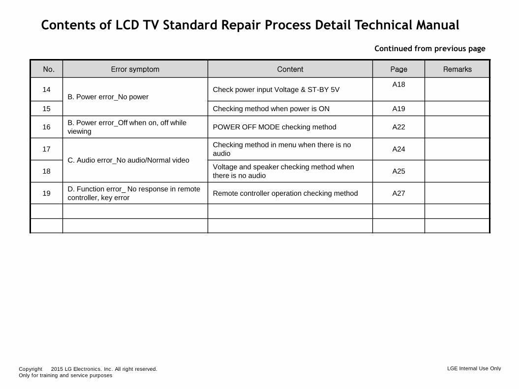
Standard Repair Process Detail Technical Manual
LCD TV connection diagram
A. Video error _Vertical/Horizontal bar, residual image, light spot
As the part connecting to the external input, check the screen condition by signal
A8
Established date
Revised date
Error
symptom
Content
A8
[MS75A]
Signage Monitor
HDMI2
/OPS
Copyright 2015 LG Electronics. Inc. All right reserved. Only for training and service purposes
LGE Internal Use Only

Standard Repair Process Detail Technical Manual
Check Link Cable reconnection condition
A. Video error_Color error
Check the contact condition of the Link Cable, especially dust or mis insertion.
A10
Established date
Revised date
Error
symptom
Content
A10
Signage Monitor
Copyright 2015 LG Electronics. Inc. All right reserved. Only for training and service purposes
LGE Internal Use Only

Standard Repair Process Detail Technical Manual
Adjustment Test pattern - ADJ Key
A. Video error_Color error
You can view 6 types of patterns using the ADJ Key
Checking item : 1. Defective pixel 2. Residual image 3. MODULE error (ADD-BAR,SCAN BAR..)
4.Video error (Classification of MODULE or Main-B/D!)
A12
Established date
Revised date
Error
symptom
Content
A12
Signage Monitor
Copyright 2015 LG Electronics. Inc. All right reserved. Only for training and service purposes
LGE Internal Use Only

Solder defect, CNT Broken
T-Con Defect, CNT Broken T-Con Defect, CNT Broken T-Con Defect, CNT Broken
Solder defect, CNT Broken Solder defect, CNT Broken
Solder defect, CNT Broken Solder defect, CNT Broken Abnormal Power Section
Solder defect, Short/Crack Abnormal Power Section Solder defect, Short/Crack
Appendix : Exchange LVDS Cable or Main B/D (1)
Copyright 2015 LG Electronics. Inc. All right reserved. Only for training and service purposes
LGE Internal Use Only

Abnormal Power Section Solder defect, Short/Crack Abnormal Power Section
Solder defect, Short/Crack Fuse Open, Abnormal power section
Noise GRADATION GRADATION
Abnormal Display
Appendix : Exchange LVDS Cable or Main B/D (2)
Copyright 2015 LG Electronics. Inc. All right reserved. Only for training and service purposes
LGE Internal Use Only

No picture/Sound Ok
Appendix : Exchange Power Board
No Light Dim Light
Dim Light Dim Light
A - 3/5
Copyright 2015 LG Electronics. Inc. All right reserved. Only for training and service purposes
LGE Internal Use Only

Appendix : Exchange the Module (1)
Panel Mura, Light leakage Press damage
Crosstalk Crosstalk Press damage
Panel Mura, Light leakage
Press damage
A - 4/5
Un-repairable Cases
In this case please exchange the module.
Copyright 2015 LG Electronics. Inc. All right reserved. Only for training and service purposes
LGE Internal Use Only

Vertical Block Source TAB IC Defect
Horizontal Block
Gate TAB IC Defect Gate TAB IC Defect Gate TAB IC Defect
Vertical Line Source TAB IC Defect
Vertical Block Source TAB IC Defect
Horizontal Block
Gate TAB IC Defect
Horizontal line
Gate TAB IC Defect
Gate TAB IC Defect Horizontal Block
Gate TAB IC Defect
Appendix : Exchange the Module (2)
A - 5/5
Un-repairable Cases
In this case please exchange the module.
Copyright 2015 LG Electronics. Inc. All right reserved. Only for training and service purposes
LGE Internal Use Only

24 Pin (Power Board ↔ Main Board)
SMAW200-H24S2
1 Power on 2 24V
3 24V 4 24V
5 GND 6 GND
7 GND 8 GND
9 3.5V 10 3.5V
11 3.5V 12 3.5V
13 GND 14 GND
15 GND 16 N.C
17 12V 18 Inverter On
19 12V 20 PWM#1
21 12V 22 PWM#2
23 N.C 24 ERROR
Standard Repair Process Detail Technical Manual
Check power input voltage and ST-BY 3.5V
B. Power error _No power
A18
Established date
Revised date
Error
symptom
Content
A18
Check DC 3.5V
Signage Monitor
Copyright 2015 LG Electronics. Inc. All right reserved. Only for training and service purposes
LGE Internal Use Only

24 Pin (Power Board ↔ Main Board)
SMAW200-H24S2
1 Power on 2 24V
3 24V 4 24V
5 GND 6 GND
7 GND 8 GND
9 3.5V 10 3.5V
11 3.5V 12 3.5V
13 GND 14 GND
15 GND 16 N.C
17 12V 18 Inverter On
19 12V 20 PWM#1
21 12V 22 PWM#2
23 N.C 24 ERROR
Standard Repair Process Detail Technical Manual
Checking method when power is ON
B. Power error _No power
A19
Established date
Revised date
Error
symptom
Content
A19
Check “power on(Pin 1)” pin is high(about 3.3V)
Signage Monitor
Copyright 2015 LG Electronics. Inc. All right reserved. Only for training and service purposes
LGE Internal Use Only

Entry method
1. Press the IN-START button of the remote controller
for adjustment
2. Check the entry into adjustment item 3
Standard Repair Process Detail Technical Manual
POWER OFF MODE checking method
B. Power error _Off when on, off whiling viewing
<ALL MODELS>
A22
Established date
Revised date
Error
symptom
Content
A22
Signage Monitor
Copyright 2015 LG Electronics. Inc. All right reserved. Only for training and service purposes
LGE Internal Use Only

Checking method 1. Press the MENU button on the remote controller for five seconds.
2. A balloon is marked to a screen. 3. Select the Speaker of Signage Setup 4. Select “ON”
Standard Repair Process Detail Technical Manual
Checking method in menu when there is no audio
C. Audio error_No audio/Normal video
<ALL MODELS>
A24
Established date
Revised date
Error
symptom
Content
A24
Signage Monitor
5 Sec
Copyright 2015 LG Electronics. Inc. All right reserved. Only for training and service purposes
LGE Internal Use Only

24 Pin (Power Board ↔ Main Board)
SMAW200-H24S2
1 Power on 2 24V
3 24V 4 24V
5 GND 6 GND
7 GND 8 GND
9 3.5V 10 3.5V
11 3.5V 12 3.5V
13 GND 14 GND
15 GND 16 N.C
17 12V 18 Inverter On
19 12V 20 PWM#1
21 12V 22 PWM#2
23 N.C 24 ERROR
Checking order when there is no audio
① Check the contact condition of or 24V connector of Main Board
② Measure the 24V input voltage supplied from Power Board (If there is no input voltage, remove and check the connector)
③ Connect the tester RX1 to the speaker terminal and if you hear the Chik Chik sound when you touch the GND and output terminal, the speaker is normal.
Standard Repair Process Detail Technical Manual
Voltage and speaker checking method when there is no audio
C. Audio error_No audio/Normal video
A25
Established date
Revised date
Error
symptom
Content
A25
[MS75A]
< Main Ass’y>
① ②
Signage Monitor
Copyright 2015 LG Electronics. Inc. All right reserved. Only for training and service purposes
LGE Internal Use Only

Checking order 1. Check IR cable condition between IR & Main board 2. Check the st-by 3.5V on the terminal M1.
3. When checking the Pre-Amp when the power is in ON condition, it is normal when the Analog
Tester needle moves slowly, and defective when it does not move at all.
Standard Repair Process Detail Technical Manual
Remote controller operation checking method
D. Function error_ No response in remote controller,
key error
A27
Established date
Revised date
Error
symptom
Content
A27
JK1401
M7 GND
M4 +3.5V_ST
M3 NC
M1 IR
M6 SCL
M5 SDA
JK1401
[MS75A Model]
Signage Monitor
Copyright 2015 LG Electronics. Inc. All right reserved. Only for training and service purposes
LGE Internal Use Only
Related Documents