Nonlocal laser annealing to improve thermal contacts between multi-layer graphene and metals This article has been downloaded from IOPscience. Please scroll down to see the full text article. 2013 Nanotechnology 24 155301 (http://iopscience.iop.org/0957-4484/24/15/155301) Download details: IP Address: 201.82.243.46 The article was downloaded on 29/03/2013 at 01:18 Please note that terms and conditions apply. View the table of contents for this issue, or go to the journal homepage for more Home Search Collections Journals About Contact us My IOPscience

Welcome message from author
This document is posted to help you gain knowledge. Please leave a comment to let me know what you think about it! Share it to your friends and learn new things together.
Transcript

Nonlocal laser annealing to improve thermal contacts between multi-layer graphene and
metals
This article has been downloaded from IOPscience. Please scroll down to see the full text article.
2013 Nanotechnology 24 155301
(http://iopscience.iop.org/0957-4484/24/15/155301)
Download details:
IP Address: 201.82.243.46
The article was downloaded on 29/03/2013 at 01:18
Please note that terms and conditions apply.
View the table of contents for this issue, or go to the journal homepage for more
Home Search Collections Journals About Contact us My IOPscience

IOP PUBLISHING NANOTECHNOLOGY
Nanotechnology 24 (2013) 155301 (10pp) doi:10.1088/0957-4484/24/15/155301
Nonlocal laser annealing to improvethermal contacts between multi-layergraphene and metals
Victor A Ermakov1, Andrei V Alaferdov1,Alfredo R Vaz1, Alexander V Baranov2 and Stanislav A Moshkalev1
1 Center for Semiconductor Components, State University of Campinas, CP 6101, Campinas, SP,13083-870, Brazil2 Saint-Petersburg State University of Information Technologies, Mechanics and Optics,49 Kronverksky Avenue, 197101 St Petersburg, Russia
E-mail: [email protected]
Received 4 February 2013, in final form 4 March 2013Published 22 March 2013Online at stacks.iop.org/Nano/24/155301
AbstractThe accuracy of thermal conductivity measurements by the micro-Raman technique forsuspended multi-layer graphene flakes has been shown to depend critically on the quality ofthe thermal contacts between the flakes and the metal electrodes used as the heat sink. Thequality of the contacts can be improved by nonlocal laser annealing at increased power. Theimprovement of the thermal contacts to initially rough metal electrodes is attributed to localmelting of the metal surface under laser heating, and increased area of real metal–graphenecontact. Improvement of the thermal contacts between multi-layer graphene and a siliconoxide surface was also observed, with more efficient heat transfer from graphene as comparedwith the graphene–metal case.
(Some figures may appear in colour only in the online journal)
Potential applications of graphene for thermal management inelectronic devices are very promising, as the in-plane thermalconductivity of single-layer graphene is extremely high: up to5.3 × 103 W m−1 K−1, according to a pioneering work ofBalandin et al [1]. A number of techniques have been used tomeasure the thermal conductivity K of single-layer, few-layerand multi-layer graphene (SLG, FLG and MLG, respectively),including optothermal micro-Raman [2–6], thermal bridge [7]and four-point probe [8] methods, where sample heating andlocal temperature measurements are realized by either opticalor electrical means.
With increasing number N of layers in MLG, the thermalconductivity K has been shown to decrease rapidly, reachingthe value for bulk graphite (near 1000 W m−1 K−1 at roomtemperature) for N > 5 [4]. The theoretical studies predict aK value for ideal infinite SLG as high as 104 W m−1 K−1 [9];however, reported experimental values vary widely, from 600to 5000 W m−1 K−1. This variation can be attributed in partto the difficulties of preparing and transferring high-quality
(defectless) graphene with well defined number of layers, aswell as to uncertainties in the laser absorbed power, finitesize of the laser spot, contribution of impurities and edgeeffects [10, 11]. One more source of uncertainties in Kmeasurements is related to poor thermal contacts betweenthe graphene and the metal electrodes. Heat transfer throughcontacts and interfaces between nanostructured materialsis an important issue in nanoelectronics, and in studiesof nanocomposites and thermal interface materials, butit is still poorly understood and the existing models ofelectrical and thermal (macro)contacts are often inapplicableat the nanoscale [12, 13]. In conventional electronic devices,interfaces between two thermally dissimilar materials likemetals and semiconductors are assumed to be planar andperfectly matched. In reality, the contact thermal resistancebetween nanostructured materials is determined by twofactors: the overlap of phonon states for two solids andthe properties of the interface itself (roughness, adhesionbetween materials). The heat transfer between two solids in
10957-4484/13/155301+10$33.00 c© 2013 IOP Publishing Ltd Printed in the UK & the USA

Nanotechnology 24 (2013) 155301 V A Ermakov et al
a perfect contact (strong bond) can be calculated using adiffusive mismatch model or acoustic mismatch model (DMMor AMM, respectively) [13, 14]. The efforts to improvethe thermal interface models continue [15–17]; however, theexisting models are based on various simplifying assumptionsand often fail to describe real nanoscale systems composedof materials with large differences in mechanical and thermalproperties. In particular, graphene materials are characterizedby extremely high anisotropy (in-plane/cross-plane cases) andlarge vibrational mismatch with most solid materials usedin nanoelectronics. The maximum vibrational frequenciesin graphene are much higher than those in metals [18,19] (45 THz compared to 7–10 THz in metals), withthe difference being smaller for oxides [20, 21]. The sp2
bonding in graphene is responsible for high elastic stiffnessin the basal plane, while rough metal surfaces can sufferplastic deformation at short length scale (at point contacts)under heating and pressure [22]. The existing models havedifficulties also in describing weakly interacting solids withsmall adhesion energy. This is the case for graphene supportedover most metals or oxides like SiO2 that do not formchemical bonds with carbon. The energy of adhesion ofgraphene to amorphous SiO2 has been recently measured tobe 0.45 and 0.31 J m−2 for SLG and FLG, respectively [23],being slightly higher for metals like Cu (0.72 J m−2) [24] and(fcc) Ni (0.81 J m−2) [25], respectively. Adhesion betweengraphene and metals can be calculated using moleculardynamics (MD) simulations [13, 25]. MD simulations wereshown to be useful also for analyses of the effects of atomisticchanges (impurities, defects, strain) on thermal propertiesof materials and interfaces [26]. Using the modified AMMmethod, Prasher [16] has shown that reduced adhesion impliessignificantly lower heat transfer between two materials. Itshould be noted, however, that even low adhesion betweentwo surfaces produces some pressure, squeezing the materialsagainst each other, and this is especially important whenplastic deformation of contacting materials is possible. Thereal area of contact between rough materials (or betweenrough and plane materials) can be just a small fraction ofthe nominal contact area. Then the local pressure due toadhesion at the isolated contact points under heat flow caneventually produce a kind of ‘welding’ between two solidsurfaces, resulting in a significant increase of the real contactarea and decrease of the thermal contact resistance [22, 27].Multi-layer graphene is essentially a rigid structure with anatomically flat surface that cannot conform to rough metalsurfaces. Therefore, for MLG–metal contact improvement,the metal surface must be smoothed. Alternatively, for metalsthat can interact chemically with carbon forming carbides(like tungsten), stronger thermal contact can be establishedat high enough annealing temperature [28]. The adhesionenergy can also be increased through the functionalizationof contacting surfaces, replacing a weak Van der Waalsinteraction by stronger covalent bonding [29].
The quality of thermal contacts is characterized bythe thermal contact resistance Rth (or thermal boundaryconductance G) [26, 27], which can be calculated by using
the equation
G = (Rth)−1= Q/(S1T), (1)
where Q is the heat flow through the interface (absorbed laserpower), S is the contact area, and 1T is the temperature dropat the interface. Schmidt et al [31] obtained experimentalvalues of the metal–graphite (HOPG) thermal boundaryconductance (TBC) at room temperature (RT) of ∼3 ×10⁷ W m−2 K−1 for Au, ∼5 × 10⁷ W m−2 K−1 for Crand Al, and ∼108 W m−2 K−1 for Ti. Similar data forAu–HOPG interfaces were reported by Norris et al [15]: near3 × 107 W m−2 K−1 at RT for as cleaved HOPG surfaces.Much higher values were obtained by Hirotani et al [32],in a study of thermal interfaces between Au and graphiticlayers (c-axis) in ∼100 nm diameter MWCNTs, varying from8.6× 107 to 2.2× 10⁸ W m−2 K−1.
The TBC between single-layer or few-layer graphene(1.2–3.0 nm thick) and amorphous SiO2 was measured torange from ∼0.8 × 10⁸ to ∼2 × 10⁸ W m−2 K−1, withno clear dependence on the number of layers, by Chenet al [33]. Different models give values varying from 6 ×10⁷ W m−2 K−1 [34] to 3 × 10⁸ W m−2 K−1 [22] for aperfectly flat graphene–amorphous SiO2 interface at RT. Evenhigher TBC can be expected for graphene interfaces withcrystalline oxide materials like sapphire [35].
In brief, for graphene (c-axis) interfaces with metals,the TBC values measured in most studies vary from 3 ×10⁷ W m−2 K−1 to 1× 10⁸ W m−2 K−1 at room temperature,whereas higher values are measured for silicon oxide, up to2 × 108 W m−2 K−1. It should be emphasized also thatexperimental methods may give reduced TBC values formetals in particular, as real contact areas for rough metalsurfaces are lower than nominal graphene/metal contact areas,while less difference can be expected for graphene/siliconoxide (smooth) surfaces. In practice, the presence of a thermalcontact resistance together with a small contact area meansthat a considerable temperature drop (tens to hundreds K) canappear at interfaces between two dissimilar materials underheat flow. Such high temperatures can result in grapheneburning and failure of the nanodevices, and also can affectthe accuracy of K measurements.
In principle, high-quality thermal contacts betweengraphene and metals can be obtained using conventionalhigh-temperature annealing in vacuum. However, as shownin our previous study [36], this can induce strain inmulti-layer graphene due to the formation of tight mechanicalcontacts between graphene and metal electrodes followedby electrode shrinkage, and thus stretching of the grapheneflake. Therefore, it is desirable to perform annealing bylocally heating the graphene flake and the area of contacts,without substantial heating of the electrode bodies. Here,doing such annealing by using the same laser, resulting inmild ‘welding’ of the graphene to the initially rough metalsurface, is proposed. The micro-Raman method was usedhere for the determination of the thermal conductivity alongsuspended multi-layer graphene flakes, and the dramatic effectof localized laser thermal annealing for the improving ofthermal contacts between graphene and metals or silicon
2
Nanotechnology 24 (2013) 155301 V A Ermakov et al
oxide, as well as on the results of K measurements, has beenshown.
1. Experimental details
Multi-layer graphene flakes (platelets) were prepared by mildultrasound processing (sonication) of natural graphene flakes(Nacional de Grafite Ltda, Brazil) in N,N-dimethylformamide(DMF) solutions. The statistical study was performed to showthat most of the graphene flakes had lateral dimensions in therange from 1 to 10 µm, and thickness from 10 to 100 nm,so their aspect ratio (lateral size/thickness) usually variesnear 102, ranging from 50 to 300. Further, the MLG flakeswere deposited over metal (Au, Ti or W) electrodes using ac(1–40 MHz) dielectrophoresis [36]. Electrodes with thicknessof 100 nm and surface roughness of 1–2 nm were depositedover thermally oxidized Si (oxide thickness of about 300 nm)by plasma sputtering using conventional photolithography andlift-off processes. In some cases, we used thicker electrodescomposed of 30 nm thick Ti adhesion layers followed byup to 1 µm thick electrochemically deposited Au electrodes,and terminated by 30 nm Ti or TiW layers, the roughness ofthe electrode surface being higher in this case (∼5–10 nm).The micron size trenches (0.9–1.1 µm wide and 5 µmdeep) between electrodes were previously cut by using afocused ion beam (Nova 200 Nanolab, FEI Co.). A 473 nmlaser focused on the sample with 100× objective (∼400 nmdiameter laser spot, maximum laser power at the sample of10.5 mW) was used for confocal Raman spectroscopy (NtegraSpectra, NT MDT). In Raman spectra, narrow grapheneG-lines (FWHM: ∼15 cm−1) and low-intensity D-lines weredetected, indicating high quality of the MLG flakes obtainedby liquid phase exfoliation from natural graphite.
The optothermal micro-Raman method [1] is based onmeasurements of the frequency downshift1ωG of a grapheneG-line with increasing temperature (in some cases, the 2D lineis used [6]), with the same laser used for local heating of thesuspended graphene samples (figure 1). From the measured1ωG value, the local graphene temperature rise 1T aboveroom temperature TRT can be estimated, using the conversioncoefficient g=1ωG/1T (cm−1 K−1), obtained in calibrationexperiments in which graphene samples are heated togetherwith substrates in hot cells. The coefficients were measured tobe −0.016, −0.015 and −0.011 cm−1 K−1 for single-layer,bi-layer and multi-layer graphene, respectively [37]. In otherstudies, values from −0.011 to −0.024 cm−1 K−1 formulti-layer graphene (or HOPG) were reported [30, 38]. Thereasons for such a discrepancy are not clear at the moment. Itmay be attributable to differing quality of samples, imperfectthermal contacts between the graphene and the heat sink,and/or different geometries in the experiments. For example,the finite size of the laser spot on a sample can affect themeasurement accuracy if it is comparable to the distancebetween the heating point and the heat sink. Here, we acceptedthe value 1ωG = −0.011 cm−1 K−1, and this has beenshown to be consistent with laser thinning experiments; seebelow. To summarize, from the measured shift value 1ωGof G-peak, the local MLG temperature rise 1T above room
Figure 1. The layout of the experiment.
temperature TRT was estimated, using the relation 1T(K) =−1ωG (cm−1)/0.011 cm−1 K−1.
Assuming that a perfect thermal contact is establishedbetween graphene and a heat sink (i.e., the room temperatureTRT is achieved at the contact point; figure 1), the temperaturegradient 1T/L = (Th − TRT)/L is estimated, where L is thedistance between the heating point and the heat sink, and This the temperature measured at the point of laser heating. Asheat sinks, metal electrodes known as good heat conductorsare commonly used. Further, using the Fourier equation the Kvalue can be calculated:
K = −PabsL/(2A1T), (2)
where Pabs is the laser power absorbed on the sample and A isthe sample cross-section area. In equation (2), we considerthat heating occurs in the center of the graphene flake andthe two electrodes contribute equally to the heat absorption.Note that heat dissipation onto the underlying substrate occurswithin the length scale given by the so called thermal healinglength LH, estimated to be ∼0.1–0.2 µm [26]. The LH valueshould be added to L in equation (2) while calculating K forshort samples.
It is generally assumed that 2.3% of laser power isabsorbed by a single graphene layer in the visible spectralrange [39]; however, in the UV region the absorption canbe higher [40], and in micro-Raman experiments done byCai et al the value of 3.3±1.1% was reported for 532 nmlaser wavelength [2]. Uncertainties in optical absorption ingraphene (due to defects, impurities, and varying numberof layers) obviously contribute to errors in estimations ofK using the micro-Raman technique. Further, it should benoted that the G-line downshift may depend on the heatingmechanism, and heating by electrical current or by lasermay result in a partial thermal equilibrium (not all phononmodes are equally excited), in contrast to the full thermalequilibrium reached in hot cells [41]. Therefore the use ofconversion coefficients determined under thermal equilibriumconditions for evaluation of local temperatures for the laserheated graphene may result in additional errors.
Nair et al [39] have shown that the reflectance of SLGis less than 0.1%. No data are available for reflectance fromfew-layer graphene; however, the reflectance of bulk graphitein the region of 500 nm was found to be as high as∼30%. ForMLG graphene, the reflectance is probably lower, but shouldapproach 30% for thick samples (>20 nm). We used here
3
Nanotechnology 24 (2013) 155301 V A Ermakov et al
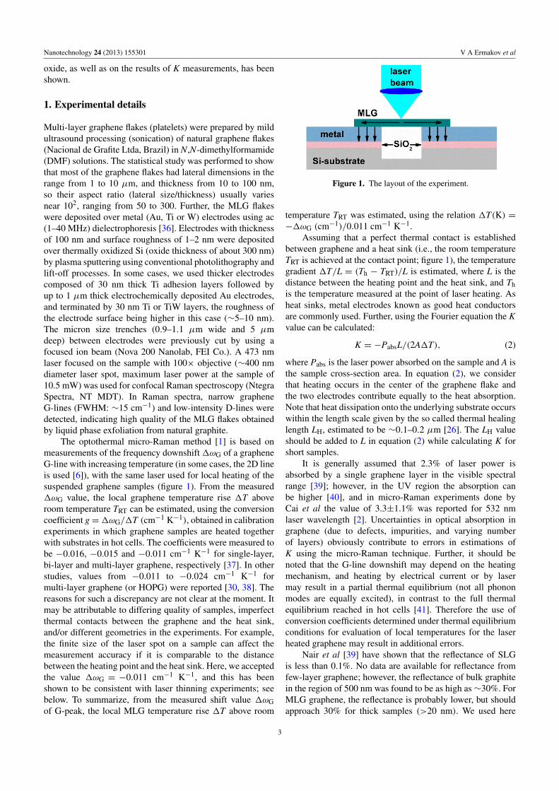
Figure 2. MLG flakes deposited over metal electrodes: W (a), Au (b) and Ti ((c), (d)), and SiO2 layers (e); (f) general view of electrodeswith several MLG flakes deposited over the gap; (a)–(c) and (e), (f) are top images, (d) is a tilted image (52◦). The scale bar corresponds to1 µm.
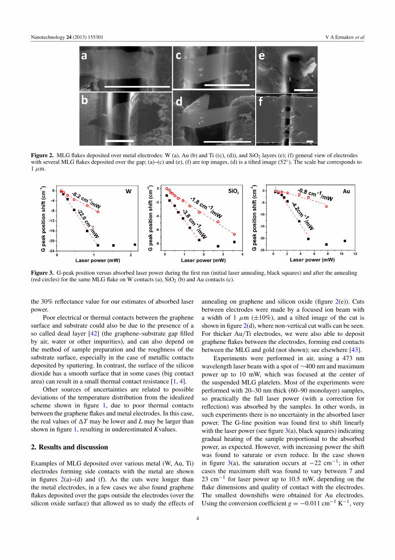
Figure 3. G-peak position versus absorbed laser power during the first run (initial laser annealing, black squares) and after the annealing(red circles) for the same MLG flake on W contacts (a), SiO2 (b) and Au contacts (c).
the 30% reflectance value for our estimates of absorbed laserpower.
Poor electrical or thermal contacts between the graphenesurface and substrate could also be due to the presence of aso called dead layer [42] (the graphene–substrate gap filledby air, water or other impurities), and can also depend onthe method of sample preparation and the roughness of thesubstrate surface, especially in the case of metallic contactsdeposited by sputtering. In contrast, the surface of the silicondioxide has a smooth surface that in some cases (big contactarea) can result in a small thermal contact resistance [1, 4].
Other sources of uncertainties are related to possibledeviations of the temperature distribution from the idealizedscheme shown in figure 1, due to poor thermal contactsbetween the graphene flakes and metal electrodes. In this case,the real values of 1T may be lower and L may be larger thanshown in figure 1, resulting in underestimated Kvalues.
2. Results and discussion
Examples of MLG deposited over various metal (W, Au, Ti)electrodes forming side contacts with the metal are shownin figures 2(a)–(d) and (f). As the cuts were longer thanthe metal electrodes, in a few cases we also found grapheneflakes deposited over the gaps outside the electrodes (over thesilicon oxide surface) that allowed us to study the effects of
annealing on graphene and silicon oxide (figure 2(e)). Cutsbetween electrodes were made by a focused ion beam witha width of 1 µm (±10%), and a tilted image of the cut isshown in figure 2(d), where non-vertical cut walls can be seen.For thicker Au/Ti electrodes, we were also able to depositgraphene flakes between the electrodes, forming end contactsbetween the MLG and gold (not shown); see elsewhere [43].
Experiments were performed in air, using a 473 nmwavelength laser beam with a spot of∼400 nm and maximumpower up to 10 mW, which was focused at the center ofthe suspended MLG platelets. Most of the experiments wereperformed with 20–30 nm thick (60–90 monolayer) samples,so practically the full laser power (with a correction forreflection) was absorbed by the samples. In other words, insuch experiments there is no uncertainty in the absorbed laserpower. The G-line position was found first to shift linearlywith the laser power (see figure 3(a), black squares) indicatinggradual heating of the sample proportional to the absorbedpower, as expected. However, with increasing power the shiftwas found to saturate or even reduce. In the case shownin figure 3(a), the saturation occurs at −22 cm−1; in othercases the maximum shift was found to vary between 7 and23 cm−1 for laser power up to 10.5 mW, depending on theflake dimensions and quality of contact with the electrodes.The smallest downshifts were obtained for Au electrodes.Using the conversion coefficient g = −0.011 cm−1 K−1, very
4

Nanotechnology 24 (2013) 155301 V A Ermakov et al
Figure 4. (a) Layer-by-layer thinning process for MLG deposited onto oxidized Si substrate, I(G)/I(Si) ratio and temperature of the flake:+, temperature; open circles: I(G)/I(Si) ratio. The inset shows the signal evolution during the first 500 s. (b) Dependence of thinning rateversus temperature (dots: derived from experimental data; line: smoothed curve). The inset in (b) shows the evolution of the number oflayers at the final stage of thinning.
high local graphene temperatures (from 600 to 2000 ◦C) canbe estimated from the maximum G-line downshifts. The effectof saturation can be attributed to two different mechanisms.First, improvement of the thermal contact between the MLGand metal electrode can occur during sample heating; then theheat losses to the electrodes become stronger and the sampletemperature drops. Second, gradual sample thinning due tographene etching in air and thus reduced laser absorptionduring the heating process can occur, as the increasing part ofthe laser power passes through the flake without absorption.Obviously, such strong heating should inevitably result ingradual layer-by-layer graphene etching and thinning byoxygen present in the air [44, 45]. However, our results provedthis process to be relatively slow, with a maximum rate muchless than one monolayer per second for Tmax ∼ 2000 K, asrevealed by special thinning experiments; see below. Thismeans that a considerable number of spectra can be acquiredduring the thinning process before the moment when the MLGbecomes thin enough to reduce the absorption of the laser lightin the sample. Furthermore, care was taken here to keep thesample exposure at the minimum required for the acquisitionof spectra (typically, ∼1 s at Tmax), leading to minimumsample changes during the exposure.
In the thinning experiments, designed to determine themulti-layer graphene etching rate at the maximum laserpower, we deposited MLG flakes onto crystalline Si substratescovered by thermally grown 300 nm thick SiO2 layers.We applied a method to measure the thickness of FLGover Si, recently proposed by Han et al [44] and Kohet al [45], to monitor the changes in the flake thicknessduring the sample annealing in air. The method is basedon the comparison between the integrated intensities of theRaman lines of graphene (G-line) and the first-order opticalphonon peak from underlying Si (520 cm−1). The MLGthickness, before and after the thinning experiment, was alsomeasured using an atomic force microscope that allowedan independent evaluation of the thickness changes. Due tothe much lower cross-layer heat conductivity of graphiticmaterials [26, 40], absorption of the laser light in the flakeleads to strong heating mostly of the upper layers and theirlayer-by-layer etching due to interaction with oxygen and theformation of volatile products like CO or CO2. The MLG
flakes chosen for such experiments were thin enough (usually,thinner than 10 nm) for detecting the characteristic Si line(520 cm−1) from the substrate. Continuous detection of theI(G)/I(Si) ratio allowed us to track the flake thinning whilethe G-line downshift provided information about the localtemperature. Note that the method is suitable for makingreliable measurements for number of layers N up to ∼10. Forthicker flakes the relation between the I(G)/I(Si) ratio andthe number N becomes nonlinear, affecting the measurementaccuracy; however, semi-quantitative information on thesample thickness evolution can still be obtained. For thesemeasurements, only flakes with lateral dimensions exceeding1.5–2.0 µm were used, to avoid a parasitic contribution fromthe bulk Si signal collected from the area around the flake (i.e.,without absorption by the flake). Typical temporal evolutionof the I(G)/I(Si) ratio and temperature is shown in figure 4.The process of thinning (reduction of the I(G)/I(Si) ratio) wasaccompanied by gradual decrease of the sample temperature(G-line downshift) due to decreasing absorption in the flake.In figure 4, the ratio changes from 0.8 to 0.25, which translatesin evolution of N from ∼10 to ∼4, following the calibrationgiven in [45] for approximately the same conditions. It isinteresting to note that the thinning process was relativelyfast for T as high as 1500–2000 K, when ∼4 monolayerswere etched out during the first 60 s under laser irradiationwith a power of 10 mW. Note that the graphene burning ratereported by Han et al [44] at T = 1450 ◦C is considerablyhigher than that in the present work. This can probably beexplained by the much higher power used (60 mW), theeffects of the substrate, contaminations and the quality ofthe graphene. Further, under the present conditions (smallerlaser power compared to that of [44]) the thinning processwas always found to stop when the temperature reduced to∼850–900 K, when monolayer graphene was not yet reached;see figure 4. AFM measurements were performed, findingthat the minimum thickness obtained in our experiments waslimited to∼1.5–2.0 nm, compatible with the estimates of Nminnear five layers (see an example in figure 5). The temperaturewhen the graphene etching stops (near 600 ◦C) is comparablewith the results of TGA analysis by Han et al [44] forgraphene and by Pang et al [46] for nanotubes (slightly lowerT values were obtained for graphite). Interestingly, at the final
5

Nanotechnology 24 (2013) 155301 V A Ermakov et al
Figure 5. AFM measurements of multi-layer graphene thicknessbefore (blue) and after (red) laser thinning. Note that the minimumthickness of the flake after the thinning process is ∼2 nm.
stage of thinning (T < 1000 K) it was possible to observestep-like changes of the I(G)/I(Si) ratio and thus the numberof layers (see the inset for figure 4(b)), indicating basically alayer-by-layer character of the MLG thinning, where fast layerremoval is followed by very long periods (up to 700–1000 s)of small changes in the I(G)/I(Si) ratio.
Further, the quality of the graphene flakes apparentlydid not change during the annealing, as the G-line FWHMand I(D)/I(G) ratios remained at the same level (in somecases, even a small reduction of the ratio was detected). Infigure 6, one example of Raman spectra taken before andafter annealing in a thinning experiment is shown for the flakewith the G-line FWHM and I(D)/I(G) ratio of ∼15 cm−1
and ∼0.05, respectively. In general, the I(D)/I(G) ratio wasfound to vary from ∼0.01 to 0.05 for different samples (infigure 6(c), a spectrum with a small D line is shown; suchsamples were mostly used for K measurements). This is muchsmaller than observed in other studies with narrower graphenenanoribbons [26, 47] and with CVD grown graphene layerswhich are known to be more defective [5], indicating verylow density of defects and relatively large average size ofgraphene crystallites in our samples. Following the approachdeveloped by Cancado et al [48] (see also [5, 47]), the averagecrystallite size La in graphene can be found using the formulaLa ∼ 560[I(D)/I(G)]−1/E4
L, where EL is the laser photonenergy in eV. For I(D)/I(G) = 0.05,La ∼ 280 nm can beestimated—being higher for smaller ratios. The fact that anincrease of the I(D)/I(G) ratio was not observed duringannealing indicates that no additional defects (or averagecrystallite size reductions) were induced by laser processingunder the present conditions, characterized by very shortexposures (<1 s) to laser light.
The saturation of the G-line position downshift withincreasing power (figure 3) can therefore be attributed mostlyto the gradual annealing of the graphene–metal contact,resulting in improving heat transfer through the contactand thus reduced graphene heating. This is confirmed byresults obtained in the second run (performed immediately
after the first one), when much lower G-line downshiftsare detected for the same laser powers, with the curveslope of −8 × 103 cm−1 W−1 as compared with −2, 2 ×104 cm−1 W−1 for the first run (figure 3(a)). Heat lossesfrom the graphene surface due to thermal contact with air(∼105 W m−2 K−1) [49] and radiation are estimated to bemuch smaller than the absorbed laser power (∼0.1 mW and10−8 mW, respectively). Thus under the present conditionsthe main mechanism of heat loss is heat transfer throughthe graphene–metal contacts, and the reduced sample heatingduring the second run clearly indicates that improvedthermal conductivity of the graphene–metal contact afterannealing occurred during the first run. The thermal contactimprovement is likely due to partial melting of the metalsurface in contact with graphene, reducing of the initiallyhigh metal surface roughness under the graphene andcorresponding increase of the contact area and adhesionbetween surfaces (figure 7). This is possible because ofdistinctly different mechanical properties of two contactingmaterials: (i) multi-layer graphene with a perfectly flatsurface, characterized by high in-plane elastic stiffness andhigh cross-plane hardness; and (ii) a rough metal surface thatis subject to plastic deformation at nanoscale length underpressure (due to adhesion) and heat flow.
Interestingly, much weaker graphene heating wasobserved for samples deposited over SiO2 (figure 2(d)), bothbefore and after the annealing (G-line downshifts: −1.6 ×103 cm−1 W−1 and −8 × 102 cm−1 W−1, respectively).Note that the contact annealing in this case was possibleonly for higher powers (>5 mW) and lower G-line downshift(−7 cm−1) corresponding to Tmax ∼ 600 ◦C; see figure 3(b).This is a clear indication of initially better thermal contactsbetween the graphene and the thermal oxide surface that ismuch flatter (roughness: ∼0.1 nm) compared with metals (Wand Au). Note that for the oxide substrate, the maximumsample heating does not exceed ∼600 ◦C, at which no sampleburning and thinning can be expected, and thus the significantreduction of the sample heating can be attributed only toimprovement of the thermal contacts.
Note that Raman measurements provide only localvalues of the temperature (1T1 and 1T2), before and afterannealing (figure 7), while the temperature drops at thegraphene–substrate interface (1Ti1 and 1Ti2) are unknown.This leads to underestimated values of K, as real values ofthe temperature change along the graphene (1Tg) are smallerthan those measured by the micro-Raman method. Assumingthat annealing changes only the interface properties (reducing1Ti1 due to the contact area increase) and that the temperaturechange along the MLG remains the same (1Tg), one canget 1T1 = 1Tg +1Ti1,1T2 = 1Tg +1Ti2, where 1Ti1 =
Pabs/(S1G) and1Ti2 = Pabs/(S2G), S1 and S2 are real contactareas before and after annealing, and 1Tg is determinedby equation (2): 1Tg = −PabsL/(2KA). Further, assumingthat after annealing the contact area becomes close to thenominal contact area Snom (S1 � S2 ≈ Snom), estimates of thetemperature drop at the interface after annealing can be madeusing the literature data on the thermal boundary conductanceG: 1Ti2 = Pabs/(SnomG). Further, the temperature change
6
Nanotechnology 24 (2013) 155301 V A Ermakov et al
Figure 6. Raman spectra of different MLG samples: (a) the same sample before and after laser annealing, at laser power of 0.29 mW, 1 s;(b) another sample, with the spectrum obtained at laser power of 2 mW, 5 s.
along the graphene can be calculated using the results afterannealing: 1Tg = 1T2 − 1Ti2 ≈ 1T2 − Pabs/(SnomG).Then, the temperature drop at the interface before annealingand the contact area increase due to annealing can beestimated: 1Ti1 = 1T1 − 1Tg ≈ 1T1 − 1T2 + 1Ti2 =
Pabs/(S1G) and S2/S1 = 1Ti1/1Ti2, respectively. Finally,estimates were obtained to show that the corrections to 1Tgin our experiments after annealing (due to 1Ti2) can varyfrom ∼10 K (for SiO2) to 100–150 K (for metals). Thesecorrections result in considerable increase (that can reach30–40% or even more) of the calculated K values for metalelectrodes, with smaller corrections for SiO2. Note also that ifthe annealing is not complete (Snom > S2), the 1Ti2 value isin fact higher and the1Tg value is then overestimated; thus Kis still underestimated.
Using the approach described here and the 1Ti1 valuesdetermined above, estimations give G near (2.5–3) ×106 W m−2 K−1 for W and Au and 6 × 10⁷ W m−2 K−1
for SiO2 before annealing, and contact areas as low as6–8% for metals and 30% for SiO2 (see table 1). Thethermal boundary conductance strongly increased as a resultof the laser annealing, and the highest TBC was observedfor SiO2. This finding proves that heat transfer by phononsfrom graphene to silicon oxide can be even more efficientthan that to metals; see also [31, 33]. On the basis of theseobservations, two important conclusions can be drawn: (i)high-temperature (T ≥ 1000 ◦C) local annealing is necessaryto achieve reasonable quality of contacts with metal surfacesthat are usually relatively rough (although the degree ofroughness may depend on the metal deposition method); (ii)high-quality thermal contacts between two nearly atomicallyflat surfaces (MLG and silicon oxide) can be achieved atlower temperatures (T ∼ 600 ◦C). The improvement of thecontact in the latter case can be attributed to the removalof air pockets, solvent traces and other possible impurities.Experiments are currently in progress on performing laserannealing under vacuum conditions, where considerablyhigher local temperatures and better contacts could beachieved without any possible damage of the graphene.
Further, using equation (2) and corrections as discussedabove, the thermal conductivity values were estimated fora number of MLG samples before and after annealing. For
Figure 7. The scheme showing improvement of thermal contactsbetween multi-layer graphene and metal contacts during laserannealing, and the resulting changes of temperature distributionover the sample.
example, the values obtained were K ∼ 340 W m−1 K−1
and 560 W m−1 K−1 for the samples shown in figures 2(a)and (b) (400 nm and 1 µm wide, respectively; both ∼20 nmthick), near room temperature. In calculations of K usingequation (2), a thermal healing length LH of 0.1 µm wasadded to the L value, as discussed above. It is important tonote that much lower values (not exceeding 150 W m−1 K−1)were obtained for samples before laser annealing. The dataobtained (after annealing) are comparable with other reportedresults for narrow graphene samples where K is reduced dueto a strong effect of phonon scattering at edges [26, 46, 50].For instance, for narrow single-layer graphene nanoribbonssupported over SiO2 [46], K median values were measuredto be ∼80 W m−1 K−1 for samples 20–60 nm wide—muchsmaller than those measured for graphene of larger size(�0.3 µm) under the same conditions. The same trendwas observed for few-layer (3–5-layer) graphene by Wanget al [50], where K values were found be much smaller fornarrow samples, for both supported and suspended graphene,decreasing from 1250 W m−1 K−1 for a 5 µm wide sample to150 W m−1 K−1 (supported) or 170 W m−1 K−1 (suspended)for 1 µm wide samples. These data show the strong effect ofthe sample width on the graphene thermal conductivity.
It is important to emphasize again that the mainpoint of this study is to show the importance of good
7
Nanotechnology 24 (2013) 155301 V A Ermakov et al
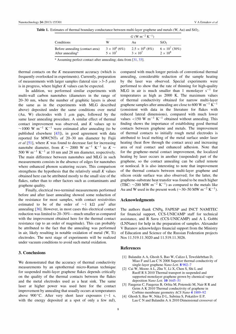
Table 1. Estimates of thermal boundary conductance between multi-layer graphene and metals (W, Au) and SiO2.
Conditions
G (W m−2 K−1)
W Au SiO2
Before annealing (contact area) 3× 10⁶ (6%) 2.5× 10⁶ (8%) 6× 10⁷ (30%)After annealinga 5× 10⁷ 3× 10⁷ 2× 10⁸
a Assuming perfect contact after annealing; data from [31, 33].
thermal contacts on the K measurement accuracy (which isfrequently overlooked in experiments). Currently, preparationof measurements with larger samples (lateral size >3–5 µm)is in progress, where higher K values can be expected.
In addition, we performed similar experiments withmulti-wall carbon nanotubes (diameters in the range of20–30 nm, where the number of graphitic layers is aboutthe same as in the experiments with MLG describedabove) deposited under the same conditions over metal(Au, W) electrodes with 1 µm gaps, followed by thesame laser annealing procedure. A similar effect of thermalcontact improvement was observed, and K values up to∼1000 W m−1 K−1 were estimated after annealing (to bepublished elsewhere [43]), in good agreement with datareported for MWCNTs of 20–30 nm diameter by Fujiiet al [51], where K was found to decrease fast for increasingnanotube diameter, from K ∼ 2000 W m−1 K−1 to K ∼500 W m−1 K−1 at 10 nm and 28 nm diameter, respectively.The main difference between nanotubes and MLG in suchmeasurements consists in the absence of edges for nanotubeswhere enhanced phonon scattering occurs. This comparisonstrengthens the hypothesis that the relatively small K valuesobtained here can be attributed mostly to the small size of theflakes, rather than to other factors such as contaminants andgraphene quality.
Finally, electrical two-terminal measurements performedbefore and after laser annealing showed some reduction ofthe resistance for most samples, with contact resistivitiesestimated to be of the order of ∼1 k� µm2 afterannealing [36]. However, in most cases this electrical contactreduction was limited to 20–30%—much smaller as comparedwith the improvement obtained here for the thermal contactresistance (up to an order of magnitude). This can probablybe attributed to the fact that the annealing was performedin air, likely resulting in notable oxidation of metal (W, Ti)electrodes. The next stage of experiments will be realizedunder vacuum conditions to avoid such metal oxidation.
3. Conclusions
We demonstrated that the accuracy of thermal conductivitymeasurements by an optothermal micro-Raman techniquefor suspended multi-layer graphene flakes depends criticallyon the quality of the thermal contacts between the flakesand the metal electrodes used as a heat sink. The samelaser at higher power was used here for the contactimprovement by annealing that usually occurs at temperaturesabove 900 ◦C. After very short laser exposures (∼1 s,with the energy deposited at a spot of only a few mJ),
compared with much longer periods of conventional thermalannealing, considerable reduction of the sample heatingby the laser was observed. Special experiments wereperformed to show that the rate of thinning for high-qualityMLG in air is much smaller than 1 monolayer s−1 fortemperatures as high as 2000 K. The maximum valuesof thermal conductivity obtained for narrow multi-layergraphene samples after annealing are close to 600 W m−1 K−1
(consistent with data in the literature for flakes withreduced lateral dimensions), compared with much lowervalues <150 W m−1 K−1 obtained without annealing. Thisfinding shows the importance of establishing good thermalcontacts between graphene and metals. The improvementof thermal contacts to initially rough metal electrodes isattributed to local melting of the metal surface under laserheating (heat flow through the contact area) and increasingarea of real contact and enhanced adhesion. Note thatfor the graphene–metal contact improvement, the localizedheating by laser occurs in another (suspended) part of thegraphene, so the contact annealing can be called remoteor nonlocal. It is also interesting to note that improvementof the thermal contacts between multi-layer graphene andsilicon oxide surface was also observed; for the latter, thegraphene–substrate heat transfer was found to be much higher(TBC: ∼200 MW m−2 K−1) as compared to the metals likeAu and W used in the present work (∼30–50 MW m−2 K−1).
Acknowledgments
The authors thank CNPq, FAPESP and INCT NAMITECfor financial support, CCS-UNICAMP staff for technicalassistance, and R Savu (CCS-UNICAMP) and A L Gobbi(LNNano) for help in the preparation of samples. AlexanderV Baranov acknowledges financial support from the Ministryof Education and Science of the Russian Federation projectsNos 11.519.11.3020 and 11.519.11.3026.
References
[1] Balandin A A, Ghosh S, Bao W, Calizo I, Teweldebrhan D,Miao F and Lau C N 2008 Superior thermal conductivity ofsingle-layer graphene Nano Lett. 8 902–7
[2] Cai W, Moore A L, Zhu Y, Li X, Chen S, Shi L andRuoff R S 2010 Thermal transport in suspended andsupported monolayer graphene grown by chemical vapordeposition Nano Lett. 10 1645–51
[3] Faugeras C, Faugeras B, Orlita M, Potemski M, Nair R R andGeim A K 2010 Thermal conductivity of graphene inCorbino membrane geometry ACS Nano 4 1889–92
[4] Ghosh S, Bao W, Nika D L, Subrina S, Pokatilov E P,Lau C N and Balandin A A 2010 Dimensional crossover of
8
Nanotechnology 24 (2013) 155301 V A Ermakov et al
thermal transport in few-layer graphene Nature Mater.9 555–8
[5] Vlassiouk V, Smirnov S, Ivanov I, Fulvio P F, Dai S,Meyer H, Chi M, Hensley D, Datskos P andLavrik N V 2011 Electrical and thermal conductivity of lowtemperature CVD graphene: the effect of disorderNanotechnology 22 275716
[6] Lee J-U, Yoon D, Kim H, Lee S W and Cheong H 2011Thermal conductivity of suspended pristine graphenemeasured by Raman spectroscopy Phys. Rev. B 83 081419
[7] Pettes M T, Jo I, Yao Z and Shi L 2011 Influence of polymericresidue on the thermal conductivity of suspended bilayergraphene Nano Lett. 11 1195–200
[8] Schwamb T, Burg B R, Schirmer N C and Poulikakos D 2009An electrical method for the measurement of the thermaland electrical conductivity of reduced graphene oxidenanostructures Nanotechnology 20 405704
[9] Evans W J, Hu L and Keblinski P 2010 Thermal conductivityof graphene ribbons from equilibrium molecular dynamics:effect of ribbon width, edge roughness, and hydrogentermination Appl. Phys. Lett. 96 203112
[10] Murali R, Yang Y, Brenner K, Beck T and Meindl J D 2009Breakdown current density of graphene nanoribbons Appl.Phys. Lett. 94 243114
[11] Chen S, Wu Q, Mishra C, Kang J, Zhang H, Cho K, Cai W,Balandin A A and Ruoff R S 2012 Thermal conductivity ofisotopically modified graphene Nature Mater. 11 203–7
[12] Leonard F and Talin A A 2011 Electrical contacts to one- andtwo-dimensional nanomaterials Nature Nanotechnol.6 773–83
[13] Chen G 2005 Nanoscale Energy Transport and Conversion(New York: Oxford University Press) p 531
[14] Swartz E T and Pohl R O 1969 Thermal boundary resistanceRev. Mod. Phys. 61 605–68
[15] Norris P M, Smoyer J L, Duda J C and Hopkins P E 2012Prediction and measurement of thermal transport acrossinterfaces between isotropic solids and graphitic materialsJ. Heat Transfer 134 020910
[16] Prasher R 2009 Acoustic mismatch model for thermal contactresistance of van der Waals contacts Appl. Phys. Lett.94 041905
[17] Beechem T, Duda J C, Hopkins P E and Norris P M 2010Contribution of optical phonons to thermal boundaryconductance Appl. Phys. Lett. 97 061907
[18] Nicklow R, Wakabayashi N and Smith H G 1972 Latticedynamics of pyrolytic graphite Phys. Rev. B 5 4951–62
[19] Pandya C V, Vyas P R, Pandya T C, Rani N andGohel V B 2011 An improved lattice mechanical model forFCC transition metals Physica B 307 138–49
[20] Sikora R 2005 An initio study of phonons in the rutilestructure of TiO2 J. Phys. Chem. Solids 66 1069–73
[21] Striefler M E and Barsch G R 1975 Lattice dynamics ofα-quartz Phys. Rev. B 12 4553–66
[22] Persson B N J, Volokitin A I and Ueba H 2011 Phononic heattransfer across an interface: thermal boundary resistanceJ. Phys.: Condens. Matter 23 045009
[23] Koenig S P, Boddeti N G, Dunn M L and Bunch J S 2011Ultrastrong adhesion of graphene membranes NatureNanotechnol. 6 543–6
[24] Yoon T, Shin W C, Kim T Y, Mun J H, Kim T-S andCho B J 2012 Direct measurement of adhesion energy ofmonolayer graphene as-grown on copper and its applicationto renewable transfer process Nano Lett. 12 1448–52
[25] Lahiri J, Miller T S, Ross A J, Adamska L, Oleynik I I andBatzill M 2011 Graphene growth and stability at nickelsurfaces New J. Phys. 13 025001
[26] Pop E, Varshney V and Roy A K 2012 Thermal properties ofgraphene: fundamentals and applications MRS Bull.37 1273–80
[27] Persson B N J, Lorenz B and Volokitin A I 2010 Heat transferbetween elastic solids with randomly rough surfaces Eur.Phys. J. E 31 3–24
[28] Luthin J and Linsmeier Ch 2000 Carbon films and carbideformation on tungsten Surf. Sci. 454–456 78–82
[29] Hopkins P E, Baraket M, Barnat E V, Beechem T E,Kearney S P, Duda J C, Robinson J T and Walton S G 2012Manipulating thermal conductance at metal–graphenecontacts via chemical functionalization Nano Lett. 12 590–5
[30] Osswald S, Flahaut E, Ye H and Gogotsi Y 2005 Eliminationof D-band in Raman spectra of double-wall carbonnanotubes by oxidation Chem. Phys. Lett. 402 422–7
[31] Schmidt A J, Collins K C, Minnich A J and Chen G 2010Thermal conductance and phonon transmissivity ofmetal–graphite interfaces J. Appl. Phys. 107 104907
[32] Hirotani J, Ikuta T, Nishiyama T and Takahashi K 2011Thermal boundary resistance between the end of anindividual carbon nanotube and a Au surfaceNanotechnology 22 315702
[33] Chen Z, Jang W, Bao W, Lau C N and Dames C 2009Thermal contact resistance between graphene and silicondioxide Appl. Phys. Lett. 95 161910
[34] Onz Z-Y and Pop E 2010 Molecular dynamics simulation ofthermal boundary conductance between carbon nanotubesand SiO2 Phys. Rev. B 81 155408
[35] Maune H, Chiu H-Y and Bockrathet M 2006 Thermalresistance of the nanoscale constrictions between carbonnanotubes and solid substrates Appl. Phys. Lett. 89 013109
[36] Rouxinol F P, Gelamo R V, Amici R G, Vaz A R andMoshkalev S A 2010 Low contact resistivity and strain insuspended multilayer graphene Appl. Phys. Lett. 97 253104
[37] Calizo I, Miao F, Bao W, Lau C N and Balandin A A 2007Variable temperature Raman microscopy as ananometrology tool for graphene layers and graphene-baseddevices Appl. Phys. Lett. 91 071913
[38] Tan P, Deng Y, Zhao Q and Cheng W 1999 The intrinsictemperature effect of the Raman spectra of graphite Appl.Phys. Lett. 74 1818–20
[39] Nair R R, Blake P, Grigorenko A N, Novoselov K S,Booth T J, Stauber T, Peres N M R and Geim A K 2008Fine structure constant defines visual transparency ofgraphene Science 320 1308
[40] Balandin A A 2011 Thermal properties of graphene andnanostructured carbon materials Nature Mater. 10 569–81
[41] Tsai C-L, Liao A, Pop E and Shim M 2011 Electrical powerdissipation in semiconducting carbon nanotubes on singlecrystal quartz and amorphous SiO2 Appl. Phys. Lett.99 053120
[42] Novoselov K S, Geim A K, Morozov S V, Jiang D, Zhang Y,Dubonos S V, Grigorieva I V and Firsov A A 2004 Electricfield effect in atomically thin carbon films Science306 666–9
[43] Alaferdov A V, Ermakov V A and Moshkalev S A 2013 atpress
[44] Han G H, Chae S J, Kim E S, Gunes F, Lee I H, Lee S W,Lee S Y, Lim S C, Jeong H K, Jeong M S and Lee Y H2010 Laser thinning for monolayer graphene formation:heat sink and interference effect ACS Nano 5 263–8
[45] Koh Y K, Bae M-H, Cahill D G and Pop E 2010 Reliablycounting atomic planes of few-layer graphene (n > 4) ACSNano 5 269–74
[46] Pang L S K, Saxby J D and Chatfield S P 1993Thermogravimetric analysis of carbon nanotubes andnanoparticles J. Phys. Chem. 97 6941–2
[47] Liao A D, Wu J Z, Wang X, Tahy K, Jena D, Dai H andPop E 2011 Thermally limited current carrying ability ofgraphene nanoribbons Phys. Rev. Lett. 106 256801
[48] Cancado L G, Takai K, Enoki T, Endo M, Kim Y A,Mizusaki H, Jorio A, Coelho L N,
9

Nanotechnology 24 (2013) 155301 V A Ermakov et al
Magalhaes-Paniago R and Primenta M A 2006 Generalequation for the determination of the crystallite size La ofnanographite by Raman spectroscopy Appl. Phys. Lett.88 163106
[49] Hsu I-K, Pettes M T, Aykol M, Shi L and Cronin S B 2010The effect of gas environment on electrical heating insuspended carbon nanotubes J. Appl. Phys. 108 084307
[50] Wang Z, Xie R, Bui C T, Liu D, Ni X, Li B andThong J T L 2010 Thermal transport in suspended andsupported few-layer graphene Nano Lett. 11 113–8
[51] Fujii M, Zhang X, Xie H, Ago H, Takahashi K, Ikuta T,Abe H and Shimizu T 2005 Measuring the thermalconductivity of a single carbon nanotube Phys. Rev. Lett.95 065502
10
Related Documents