Nonlinear-optical phase modification in dispersion-engineered Si photonic wires J. I. Dadap, 1* N. C. Panoiu, 1** Xiaogang Chen, 1 I-Wei Hsieh, 1 Xiaoping Liu, 1 Cheng- Yun Chou, 1 E. Dulkeith, 2† S. J. McNab, 2‡ Fengnian Xia, 2 W. M. J. Green, 2 L. Sekaric, 2 Y. A. Vlasov, 2 and R. M. Osgood, Jr. 1 1 Microelectronics Sciences Laboratories, Columbia University, New York, NY, 10027, USA 2 IBM T. J. Watson Research Center, Yorktown Heights, NY 10598, USA **Current Address: Department of Electronic and Electrical Engineering, University College London, Torrington Place, London WC1E 7JE, UK † Current Address: Detecon, Inc., Strategy and Innovation Engineering Group, San Mateo, CA 94402, USA ‡ Current Address: Allied Telesis Labs, 27 Nazareth Ave, Christchurch, New Zealand *Corresponding author: [email protected] Abstract: The strong dispersion and large third-order nonlinearity in Si photonic wires are intimately linked in the optical physics needed for the optical modification of phase. By carefully choosing the waveguide dimensions, both linear and nonlinear optical properties of Si wires can be engineered. In this paper we provide a review of the modification of phase using nonlinear-optical effects such as self-phase and cross-phase modulation in dispersion-engineered Si wires. The low threshold powers for phase-changing effects in Si-wires make them potential candidates for functional nonlinear optical devices of just a few millimeters in length. © 2008 Optical Society of America OCIS codes: (190.4390) Nonlinear optics, integrated optics; (130.4310) Integrated optics, Nonlinear; (190.7110) Ultrafast nonlinear optics; (060.5060) Phase modulation; (130.2790) Guided waves; (230.3990) Micro-optical devices; (230.7370) Waveguides References and links 1. R. A. Soref and J. P. Lorenzo, “Single-crystal silicon: a new material for 1.3 and 1.6 μm integrated-optical components,” Electron. Lett. 21, 953-954 (1985). 2. R. A. Soref and B. R. Bennett, “Electro-optical effects in Silicon,” IEEE J. Quantum Electron. QE-23, 123–129 (1987). 3. A. Liu, R. Jones, L. Liao, D. Samara-Rubio, D. Rubin, O. Cohen, R. Nicolaescu, and M. Paniccia, “A high- speed silicon optical modulator based on a metal-oxide-semiconductor capacitor,” Nature 427, 615–618 (2004). 4. Q. Xu, B. Shmidt, S. Pradhan, and M. Lipson, “Micrometre-scale silicon electro-optic modulator,” Nature 435, 325-327 (2005). 5. V. R. Almeida, C. A. Barrios, R. Panepucci, and M. Lipson, “All-optical control of light on a silicon chip,” Nature 431, 1081-1084 (2004). 6. C. A. Barrios, V. R. de Almeida, M. Lipson, “Low-Power-Consumption Short-Length and High-Modulation- Depth Silicon Electrooptic Modulator,” IEEE J. Lightwave Technol. 21, 1089-1098 (2003). 7. G. Cocorullo, M. Iodice, I. Rendina, and P. M. Sarro, “Silicon thermooptic micromodulator with 700-kHz - 3- dB bandwidth,” IEEE Photon. Technol. Lett. 7, 363-365 (1995). 8. R. L. Espinola, M.-C. Tsai, J. T. Yardley, and R. M. Osgood Jr., “Fast and low-power thermooptic switch on thin silicon-on-insulator,” IEEE Photon. Technol. Lett. 15, 1366–1368 (2003). 9. M. Harjanne, M. Kapulainen, T. Aalto, and P. Heimala, “Sub- s switching time in silicon-on-insulator Mach- Zender thermooptic switch,” IEEE Photon. Technol. Lett. 16, 2039–2041 (2004). 10. M. W. Geis, S. J. Spector, R. C. Williamson, and T. M. Lyszczarz, “Submicrosecond, submilliwatt, silicon-on- insulator thermooptic switch,” IEEE Photon. Technol. Lett. 16, 2514–2516 (2004). 11. Y. A. Vlasov, M. O'Boyle, H. F. Hamann, and S. J. McNab, “Active control of slow light on a chip with photonic crystal waveguides,” Nature 438, 65 - 69 (2005). 12. W. Bogaerts, R. Baets, P. Dumon, V. Wiaux, S. Beckx, D. Taillaert, B. Luyssaert, J. van Campenhout, P. Bienstman, and D. van Thourhout, “Nanophotonic waveguides in silicon-on-insulator fabricated with CMOS technology,” J. Lightwave Technol. 23, 401-412 (2005). 13. R. A. Soref, “Silicon-Based Optoelectronics,” Proc. IEEE, 81, 1687-1706 (1993). 14. B. P. Pal, “Guided-wave optics on silicon: physics, technology, and status,” Progress in Optics 32, 3-59 (1994). 15. G. T. Reed and A. P. Knights, Silicon Photonics: An Introduction (John Wiley, Chichester, UK, 2004). 16. L. Pavesi and D. J. Lockwood, Silicon Photonics (Springer-Verlag, New York, 2004). #87797 - $15.00 USD Received 21 Sep 2007; revised 2 Jan 2008; accepted 3 Jan 2008; published 16 Jan 2008 (C) 2008 OSA 21 January 2008 / Vol. 16, No. 2 / OPTICS EXPRESS 1280

Welcome message from author
This document is posted to help you gain knowledge. Please leave a comment to let me know what you think about it! Share it to your friends and learn new things together.
Transcript

Nonlinear-optical phase modification in dispersion-engineered Si photonic wires
J. I. Dadap,1* N. C. Panoiu,1** Xiaogang Chen,1 I-Wei Hsieh,1 Xiaoping Liu,1 Cheng-Yun Chou,1 E. Dulkeith,2† S. J. McNab,2‡ Fengnian Xia,2 W. M. J. Green,2 L. Sekaric,2
Y. A. Vlasov,2 and R. M. Osgood, Jr.1 1Microelectronics Sciences Laboratories, Columbia University, New York, NY, 10027, USA
2IBM T. J. Watson Research Center, Yorktown Heights, NY 10598, USA **Current Address: Department of Electronic and Electrical Engineering, University College London,
Torrington Place, London WC1E 7JE, UK †Current Address: Detecon, Inc., Strategy and Innovation Engineering Group, San Mateo, CA 94402, USA
‡Current Address: Allied Telesis Labs, 27 Nazareth Ave, Christchurch, New Zealand
*Corresponding author: [email protected]
Abstract: The strong dispersion and large third-order nonlinearity in Si photonic wires are intimately linked in the optical physics needed for the optical modification of phase. By carefully choosing the waveguide dimensions, both linear and nonlinear optical properties of Si wires can be engineered. In this paper we provide a review of the modification of phase using nonlinear-optical effects such as self-phase and cross-phase modulation in dispersion-engineered Si wires. The low threshold powers for phase-changing effects in Si-wires make them potential candidates for functional nonlinear optical devices of just a few millimeters in length.
© 2008 Optical Society of America
OCIS codes: (190.4390) Nonlinear optics, integrated optics; (130.4310) Integrated optics, Nonlinear; (190.7110) Ultrafast nonlinear optics; (060.5060) Phase modulation; (130.2790) Guided waves; (230.3990) Micro-optical devices; (230.7370) Waveguides
References and links
1. R. A. Soref and J. P. Lorenzo, “Single-crystal silicon: a new material for 1.3 and 1.6 μm integrated-optical components,” Electron. Lett. 21, 953-954 (1985).
2. R. A. Soref and B. R. Bennett, “Electro-optical effects in Silicon,” IEEE J. Quantum Electron. QE-23, 123–129 (1987).
3. A. Liu, R. Jones, L. Liao, D. Samara-Rubio, D. Rubin, O. Cohen, R. Nicolaescu, and M. Paniccia, “A high-speed silicon optical modulator based on a metal-oxide-semiconductor capacitor,” Nature 427, 615–618 (2004).
4. Q. Xu, B. Shmidt, S. Pradhan, and M. Lipson, “Micrometre-scale silicon electro-optic modulator,” Nature 435, 325-327 (2005).
5. V. R. Almeida, C. A. Barrios, R. Panepucci, and M. Lipson, “All-optical control of light on a silicon chip,” Nature 431, 1081-1084 (2004).
6. C. A. Barrios, V. R. de Almeida, M. Lipson, “Low-Power-Consumption Short-Length and High-Modulation-Depth Silicon Electrooptic Modulator,” IEEE J. Lightwave Technol. 21, 1089-1098 (2003).
7. G. Cocorullo, M. Iodice, I. Rendina, and P. M. Sarro, “Silicon thermooptic micromodulator with 700-kHz - 3-dB bandwidth,” IEEE Photon. Technol. Lett. 7, 363-365 (1995).
8. R. L. Espinola, M.-C. Tsai, J. T. Yardley, and R. M. Osgood Jr., “Fast and low-power thermooptic switch on thin silicon-on-insulator,” IEEE Photon. Technol. Lett. 15, 1366–1368 (2003).
9. M. Harjanne, M. Kapulainen, T. Aalto, and P. Heimala, “Sub-μs switching time in silicon-on-insulator Mach-Zender thermooptic switch,” IEEE Photon. Technol. Lett. 16, 2039–2041 (2004).
10. M. W. Geis, S. J. Spector, R. C. Williamson, and T. M. Lyszczarz, “Submicrosecond, submilliwatt, silicon-on-insulator thermooptic switch,” IEEE Photon. Technol. Lett. 16, 2514–2516 (2004).
11. Y. A. Vlasov, M. O'Boyle, H. F. Hamann, and S. J. McNab, “Active control of slow light on a chip with photonic crystal waveguides,” Nature 438, 65 - 69 (2005).
12. W. Bogaerts, R. Baets, P. Dumon, V. Wiaux, S. Beckx, D. Taillaert, B. Luyssaert, J. van Campenhout, P. Bienstman, and D. van Thourhout, “Nanophotonic waveguides in silicon-on-insulator fabricated with CMOS technology,” J. Lightwave Technol. 23, 401-412 (2005).
13. R. A. Soref, “Silicon-Based Optoelectronics,” Proc. IEEE, 81, 1687-1706 (1993). 14. B. P. Pal, “Guided-wave optics on silicon: physics, technology, and status,” Progress in Optics 32, 3-59 (1994). 15. G. T. Reed and A. P. Knights, Silicon Photonics: An Introduction (John Wiley, Chichester, UK, 2004). 16. L. Pavesi and D. J. Lockwood, Silicon Photonics (Springer-Verlag, New York, 2004).
#87797 - $15.00 USD Received 21 Sep 2007; revised 2 Jan 2008; accepted 3 Jan 2008; published 16 Jan 2008
(C) 2008 OSA 21 January 2008 / Vol. 16, No. 2 / OPTICS EXPRESS 1280

17. M. Paniccia, M. Morse, and M. Salib, “Integrated Photonics,” Top. Appl. Phys. 94, 51-88 (2004). 18. L. C. Kimerling, L. Dal Negro, S. Saini, Y. Yi, D. Ahn, S. Akiyama, D. Cannon, J. Liu, J. G. Sandland, D.
Sparacin, J. Michel, K. Wada, and M. R. Watts, “Monolithic Silicon Microphotonics,” Top. Appl. Phys. 94, 89-120 (2004).
19. B. Jalali, R. Claps, D. Dimitropoulos, and V. Raghunathan, “Light generation, amplification, and wavelength conversion via stimulated Raman scattering in silicon microstructures,” Top. Appl. Phys. 94, 199–238 (2004).
20. R. J. Bozeat, S. Day, F. Hopper, F. P. Payne, S. W. Roberts, and M. Asghari, “Silicon Based Waveguides,” Top. Appl. Phys. 94, 269-294 (2004).
21. S. Janz, “Silicon-Based Waveguide Technology for Wavelength Division Multiplexing,” Top. Appl. Phys. 94, 323-360 (2004).
22. A. Irace, G. Breglio, M. Iodice and A. Cutolo, “Light Modulation with Silicon Devices,” Top. Appl. Phys. 94, 361-391 (2004).
23. M. Lipson, “Guiding, modulating, and emitting light on silicon - challenges and opportunities,” J. Lightwave Technol. 23, 4222-4238 (2005).
24. L. Pavesi and G. Guillot, Optical Interconnects - the silicon approach (Springer-Verlag, Heidelberg, 2006). 25. B. Jalali and S. Fathpour, “Silicon photonics,” J. Lightwave Technol. 24, 4600-4615 (2006). 26. R. A. Soref, "The past, present, and future of silicon photonics," IEEE J. Sel. Top. Quantum Electron. 12, 1678-
1687 (2006). 27. P. Dumon, G. Priem, L. R. Nunes, W. Bogaerts, D. van Thourhout, P. Bienstman, T. K. Liang, M. Tsuchiya,
P. Jaenen, S. Beckx, J. Wouters, and R. Baets, “Linear and nonlinear nanophotonic devices based on silicon-on-insulator wire waveguides,” Jpn. J. Appl. Phys. 45, 6589-6602 (2006).
28. R Dekker, N Usechak, M Först, and A Driessen, “Ultrafast nonlinear all-optical processes in silicon-on-insulator waveguides,” J. Phys. D: Appl. Phys. 40, R249-R271 (2007).
29. R. Claps, D. Dimitropoulos, Y. Han, and B. Jalali, “Observation of Raman emission in silicon waveguides at 1.54 μm,” Opt. Express 10, 1305-1313 (2002).
30. J. I. Dadap, R. L. Espinola, R. M. Osgood, Jr., S. J. McNab, and Y. A. Vlasov, “Spontaneous Raman scattering in ultrasmall silicon waveguides,” Opt. Lett. 29, 2755-2757 (2004).
31. R. Claps, D. Dimitropoulos, V. Raghunathan, Y. Han, and B. Jalali, “Observation of stimulated Raman amplification in silicon waveguides,” Opt. Express 11, 1731-1739 (2003).
32. R. Espinola, J. I. Dadap, R. M. Osgood, S. J. McNab, and Y. A. Vlasov, “Raman amplification in ultrasmall silicon-on-insulator wire waveguides,” Opt. Express 12, 3713-3718 (2004).
33. T. K. Liang and H. K. Tsang, “Efficient Raman amplification in silicon-on-insulator waveguides,” Appl. Phys. Lett. 85, 3343-3345 (2004).
34. A. Liu, H. Rong, M. Paniccia, O. Cohen, and D. Hak, “Net optical gain in a low loss silicon-on-insulator waveguide by stimulated Raman scattering,” Opt. Express 12, 4261-4268 (2004).
35. Ö. Boyraz and B. Jalali, “Demonstration of 11dB fiber-to-fiber gain in a silicon Raman amplifier,” IEICE Elect.Express 1, 429-434 (2004).
36. Q. Xu, V. R. Almeida, and M. Lipson, “Demonstration of high Raman gain in a submicrometer-size silicon-on-insulator waveguide,” Opt. Lett. 30, 35-37 (2005).
37. R. Claps, V. Raghunathan, Ö. Boyraz, P. Koonath, D. Dimitropoulos, and B. Jalali, “Raman amplification and lasing in SiGe waveguides,” Opt. Express 13, 2459-2466 (2005).
38. S. G. Cloutier, P. A. Kossyrev, and J. Xu, “Optical gain and stimulated emission in periodic nanopatterned crystalline silicon,” Nature Materials 4, 887-891 (2005).
39. J. F. McMillan, X. Yang, N. C. Panoiu, R. M. Osgood, and C. W. Wong, “Enhanced stimulated Raman scattering in slow-light photonic crystal waveguides,” Opt. Lett. 31, 1235-1237 (2006).
40. Ö. Boyraz and B. Jalali, “Demonstration of a silicon Raman laser,” Opt. Express 12, 5269-5273 (2004). 41. H. Rong, A. Liu, R. Jones, O. Cohen, D. Hak, R. Nicolaescu, A. Fang, and M. Paniccia, “An all-silicon Raman
laser,” Nature 433, 292–294 (2005). 42. H. Rong, R. Jones, A. Liu, O. Cohen, D. Hak, A. Fang, and M. Paniccia, “A continuous-wave Raman silicon
laser,” Nature 433, 725 (2005). 43. Ö. Boyraz and B. Jalali, “Demonstration of a directly modulated silicon Raman laser,” Opt. Express 13, 796-800
(2005). 44. H. Rong, Y. -H. Kuo, S. Xu, A. Liu, R. Jones, M. Paniccia, O. Cohen, and O. Raday, “Monolithic integrated
Raman silicon laser,” Opt. Express 14, 6705-6712 (2006). 45. A. Polman, B. Min, J. Kalkman, T. J. Kippenberg, and K. J. Vahala, “Ultra-low threshold erbium-implanted
toroidal microlaser on silicon,” Appl. Phys. Lett. 84, 1037-1039 (2004). 46. A. W. Fang, H. Park, O. Cohen, R. Jones, M. J. Paniccia, and J. E. Bowers, “Electrically pumped hybrid
AlGaInAs-silicon evanescent laser,” Opt. Express 14, 9203-9210 (2006). 47. R. Claps, V. Raghunathan, D. Dimitropoulos, and B. Jalali, “Anti-Stokes Raman conversion in silicon
waveguides,” Opt. Express 11, 2862-2872 (2003). 48. V. Raghunathan, R. Claps, D. Dimitropoulos, and B. Jalali, “Parametric Raman wavelength conversion in scaled
silicon waveguides,” J. Lightwave Technol. 23, 2094-2102 (2005). 49. R. Espinola, J. Dadap, R. Osgood, Jr., S. McNab, and Y. Vlasov, “C-band wavelength conversion in silicon
photonic wire waveguides,” Opt. Express 13, 4341-4349 (2005). 50. H. Fukuda, K. Yamada, T. Shoji, M. Takahashi, T. Tsuchizawa, T. Watanabe, J. -i. Takahashi, and S. -i. Itabashi,
“Four-wave mixing in silicon wire waveguides,” Opt. Express 13, 4629-4637 (2005). 51. Q. Xu, V. R. Almeida, and M. Lipson, “Micrometer-scale all-optical wavelength converter on silicon,” Opt. Lett.
30, 2733-2735 (2005).
#87797 - $15.00 USD Received 21 Sep 2007; revised 2 Jan 2008; accepted 3 Jan 2008; published 16 Jan 2008
(C) 2008 OSA 21 January 2008 / Vol. 16, No. 2 / OPTICS EXPRESS 1281

52. Y. -H. Kuo, H. Rong, V. Sih, S. Xu, M. Paniccia, and O. Cohen, “Demonstration of wavelength conversion at 40 Gb/s data rate in silicon waveguides,” Opt. Express 14, 11721-11726 (2006).
53. M. A. Foster, A. C. Turner, J. E. Sharping, B. S. Schmidt, M. Lipson, and A. L. Gaeta, “Broadband optical parametric gain on a silicon photonic chip,” Nature 441, 960-963 (2006).
54. K. Yamada, H. Fukuda, T. Tsuchizawa, T. Watanabe, T. Shoji, and S. Itabashi, “All-optical efficient wavelength conversion using silicon photonic wire waveguide,” IEEE Photon. Technol. Lett. 18, 1046-1048 (2006).
55. Q. Lin, J. Zhang, P. M. Fauchet, and G. P. Agrawal, “Ultrabroadband parametric generation and wavelength conversion in silicon waveguides,” Opt. Express 14, 4786-4799 (2006).
56. H.K. Tsang, C.S. Wong, T.K. Lang, I.E. Day, S.W. Roberts, A. Harpin, J. Drake, and M. Asghari, “Optical dispersion, two-photon absorption and self-phase modulation in silicon waveguides at 1.5 µm wavelength,” Appl. Phys. Lett. 3, 416-418 (2002).
57. G. W. Rieger, K. S. Virk, and J. F. Young, “Nonlinear propagation of ultrafast 1.5 µm pulses in high-index-contrast silicon-on-insulator waveguides,” Appl. Phys. Lett. 84, 900-902 (2004).
58. Ö. Boyraz, T. Indukuri, and B. Jalali, “Self-phase modulation-induced spectral broadening in silicon waveguides,” Opt. Express 12, 829-834 (2004).
59. A. Cowan, G. Rieger, and J. Young, “Nonlinear transmission of 1.5 µm pulses through single-mode silicon-on-insulator waveguide structures,” Opt. Express 12, 1611-1621 (2004).
60. H. Yamada, M. Shirane, T. Chu, H. Yokoyama, S. Ishida, and Y. Arakawa, “Nonlinear-optic silicon-nanowire waveguides,” Jpn. J. Appl. Phys. 44, 6541-6545 (2005).
61. E. Dulkeith, Y. A. Vlasov, X. Chen, N. C. Panoiu, and R. M. Osgood, Jr., “Self-phase-modulation in submicron silicon-on-insulator photonic wires,” Opt. Express 14, 5524-5534 (2006).
62. I. -W. Hsieh, X. Chen, J. I. Dadap, N. C. Panoiu, R. M. Osgood, S. J. McNab, and Y. A. Vlasov, “Ultrafast-pulse self-phase modulation and third-order dispersion in Si photonic wire-waveguides,” Opt. Express 14, 12380-12387 (2006).
63. Ö. Boyraz, P. Koonath, V. Raghunathan, and B. Jalali, “All optical switching and continuum generation in silicon waveguides,” Opt. Express 12, 4094-4102 (2004).
64. T. Liang, L. Nunes, T. Sakamoto, K. Sasagawa, T. Kawanishi, M. Tsuchiya, G. Priem, D. Van Thourhout, P. Dumon, R. Baets, and H. Tsang, “Ultrafast all-optical switching by cross-absorption modulation in silicon wire waveguides,” Opt. Express 13, 7298-7303 (2005).
65. R. Dekker, A. Driessen, T. Wahlbrink, C. Moormann, J. Niehusmann, and M. Först, “Ultrafast Kerr-induced all-optical wavelength conversion in silicon waveguides using 1.55 μm femtosecond pulses,” Opt. Express 14, 8336-8346 (2006).
66. I. -W. Hsieh, X. Chen, J. I. Dadap, N. C. Panoiu, R. M. Osgood, Jr., S. J. McNab, and Y. A. Vlasov, “Cross-phase modulation-induced spectral and temporal effects on co-propagating femtosecond pulses in silicon photonic wires,” Opt. Express 15, 1135-1146 (2007).
67. C. Manolatou and M. Lipson, “All-optical silicon modulators based on carrier injection by two-photon absorption,” J. Lightwave Technol. 24, 1433-1439 (2006).
68. T.K. Liang, L.R. Nunes, M. Tsuchiya, K.S. Abedin, T. Miyazaki, D. Van Thourhout, W. Bogaerts, P. Dumon, R. Baets, and H.K. Tsang, “High speed logic gate using two-photon absorption in silicon waveguides,” Optics Commun. 265, 171-174 (2006).
69. I. -W. Hsieh, X. Chen, X. Liu, J. I. Dadap, N. C. Panoiu, C. -Y. Chou, F. Xia, W. M. Green, Y. A. Vlasov, and R. M. Osgood, “Supercontinuum generation in silicon photonic wires,” Opt. Express 15, 15242-15249 (2007).
70. R. W. Boyd, Nonlinear Optics, 2nd ed. (Academic Press, 2002). 71. S. McNab, N. Moll, and Y. A. Vlasov, “Ultra-low loss photonic integrated circuit with membrane-type photonic
crystal waveguides,” Opt. Express 11, 2927-2939 (2003). 72. Y. Vlasov and S. McNab, “Losses in single-mode silicon-on-insulator strip waveguides and bends,” Opt.
Express 12, 1622-1631 (2004). 73. F. Xia, L. Sekaric, and Y. A. Vlasov, “Ultracompact optical buffers on a silicon chip,” Nature Photonics 1, 65 -
71 (2007). 74. W. H. Reeves, D. V. Skryabin, F. Biancalana, J. C. Knight, P. S. J. Russell, F. G. Omenetto, A. Efimov, and A. J.
Taylor, “Transformation and control of ultra-short pulses in dispersion-engineered photonic crystal fibers,” Nature 424, 511 (2003).
75. M. Foster, K. Moll, and A. Gaeta, “Optimal waveguide dimensions for nonlinear interactions,” Opt. Express 12, 2880-2887 (2004).
76. S. Ramachandran, “Dispersion-tailored few-mode fibers: A versatile platform for in-fiber photonic devices,” J. Lightwave Technol. 23, 3426 (2005).
77. X. Chen, N. C. Panoiu, and R. M. Osgood, “Theory of Raman-mediated pulsed amplification in silicon-wire waveguides,” IEEE J. Quantum Electron. 42, 160-170 (2006).
78. E. Dulkeith, F. Xia, L. Schares, W. M. J. Green, and Y. A. Vlasov, “Group index and group velocity dispersion in silicon-on-insulator photonic wires,” Opt. Express 14, 3853-3863 (2006).
79. A. C. Turner, C. Manolatou, B. S. Schmidt, M. Lipson, M. A. Foster, J. E. Sharping, and A. L. Gaeta, “Tailored anomalous group-velocity dispersion in silicon channel waveguides,” Opt. Express 14, 4357-4362 (2006).
80. L. Yin, Q. Lin, and G. P. Agrawal, “Dispersion tailoring and soliton propagation in silicon waveguides,” Opt. Lett. 31, 1295-1297 (2006).
81. X. Chen, N. Panoiu, I. Hsieh, J. I. Dadap, and R. M. Osgood, Jr., “Third-order dispersion and ultrafast pulse propagation in silicon wire waveguides,” IEEE Photon. Technol. Lett. 18, 2617-2619 (2006).
82. T. K. Liang and H. K. Tsang, “Role of free carriers from two-photon absorption in Raman amplification in silicon-on-insulator waveguides,” Appl. Phys. Lett. 84, 2745-2747 (2004).
#87797 - $15.00 USD Received 21 Sep 2007; revised 2 Jan 2008; accepted 3 Jan 2008; published 16 Jan 2008
(C) 2008 OSA 21 January 2008 / Vol. 16, No. 2 / OPTICS EXPRESS 1282

83. R. Claps, V. Raghunathan, D. Dimitropoulos, and B. Jalali, “Influence of nonlinear absorption on Raman amplification in Silicon waveguides,” Opt. Express 12, 2774-2780 (2004).
84. M. Dinu, F. Quochi, and H. Garcia, “Third-order nonlinearities in silicon at telecom wavelengths,” Appl. Phys. Lett. 82, 2954 (2003).
85. M. Dinu, “Dispersion of phonon-assisted nonresonant third-order nonlinearities,” IEEE J. Quantum Electron. 39, 1498-1503 (2003).
86. A. D. Bristow, N. Rotenberg, and H. M. van Driel, “Two-photon absorption and Kerr coefficients of silicon for 850–2200 nm,” Appl. Phys. Lett. 90, 191104 (2007).
87. Q. Lin, J. Zhang, G. Piredda, R. W. Boyd, P. M. Fauchet, and G. P. Agrawal, “Dispersion of silicon nonlinearities in the near infrared region,” Appl. Phys. Lett. 91, 21111 (2007).
88. G. P. Agrawal, Nonlinear Fiber Optics (Academic Press, 1989). 89. C. Koos, L. Jacome, C. Poulton, J. Leuthold, and W. Freude, “Nonlinear silicon-on-insulator waveguides for all-
optical signal processing,” Opt. Express 15, 5976-5990 (2007). 90. J. Zhang, Q. Lin, G. Piredda, R. W. Boyd, G. P. Agrawal, and P. M. Fauchet, “Optical solitons in a silicon
waveguide,” Opt. Express 15, 7682-7688 (2007). 91. L. Yin, Q. Lin, and G. P. Agrawal, “Soliton fission and supercontinuum generation in silicon waveguides,” Opt.
Lett. 32, 391-393 (2007). 92. P. F. Curley, C. Spielmann, T. Brabec, F. Krausz, E. Wintner, and A. J. Schmidt, “Operation of a femtosecond
Ti:sapphire solitary laser in the vicinity of zero group-delay dispersion,” Opt. Lett. 18, 54- (1993). 93. P. K. A. Wai, C. R. Menyuk, Y. C. Lee, and H. H. Chen, “Nonlinear pulse propagation in the neighborhood of
the zero-dispersion wavelength of monomode optical fibers,” Opt. Lett. 11, 464-466 (1986). 94. N. Akhmediev and M. Karlsson, “Cherenkov radiation emitted by solitons in optical fibers,” Phys. Rev. A 51,
2602–2607 (1995). 95. P. L. Baldeck, R. R. Alfano, and G. P. Agrawal, “Induced-frequency shift of copropagating ultrafast optical
pulses,” Appl. Phys. Lett. 52, 1939-1941 (1988). 96. N. C. Panoiu, X. Chen, and R. M. Osgood, Jr., “Modulation instability in silicon photonic nanowires,” Opt. Lett.
31, 3609-3611 (2006). 97. G. P. Agrawal, “Modulation instability induced by cross-phase modulation,” Phys. Rev. Lett. 59, 880-883
(1987). 98. J. E. Rothenberg, “Modulational instability for normal dispersion,” Phys. Rev. A 42, 682-685 (1990). 99. W. Huang and J. Hong, “A coupled-mode analysis of modulation instability in optical fibers,” J. Lightwave
Technol. 10, 156-162 (1992). 100. M. Yu, C. J. Mckinstrie, and G. P. Agrawal, “Instability due to cross-phase modulation in the normal-dispersion
regime,” Phys. Rev. E 48, 2178 (1993). 101. D. Schadt and B. Jaskorzynska, “Generation of short pulses from CW light by influence of crossphase
modulation (CPM) in optical fibres,” Electron. Lett. 23, 1090-1091 (1987). 102. A. S. Gouveia-Neto, M. E. Faldon, A. S. B. Sombra, P. G. J. Wigley, and J. R. Taylor, “Subpicosecond-pulse
generation through cross-phase-modulation-induced modulational instability in optical fibers,” Opt. Lett. 13, 901-903 (1988).
103. E. -K. Tien, N. S. Yuksek, F. Qian, and Ö. Boyraz, “Pulse compression and modelocking by using TPA in silicon waveguides,” Opt. Express 15, 6500-6506 (2007).
1. Introduction
The last few years have seen an extraordinarily rapid pace in advances in developing new active silicon photonics devices and understanding their underlying physics. This area of research began more than two decades ago, with a study by Soref and Lorenzo, in which the first silicon waveguide was demonstrated [1]. Soon after, work in silicon photonics concentrated on electro-optical control through the use of free carriers (FC), e.g., by carrier injection, as a means of modulating light either by modifying the refractive index or the material absorption [2]. The results of this work led to the development of silicon-based optical modulators [3-6]. The work on free-carrier modulation in silicon was then followed by research in thermo-optic modulators, which have a surprisingly high performance due to the favorable thermo-optic coefficient of silicon [7-11]. Rapid advances in both of these device types have continued into the present, including scaling down the device “footprint” and power consumption and increasing the frequency response. Because the favorable electronic, optical, and physical properties of silicon and in conjunction with the mature complementary metal-oxide-semiconductor (CMOS) fabrication processing technology, large-scale integration of functional optical devices becomes possible, including integration with relatively complex electronic components. The use of CMOS manufacturing also facilitates its precise patterning to be applied to integrated optical circuits; this enables, for example, greatly reduced sidewall roughness and, hence, very low loss even in the small waveguides mentioned here. An excellent overview of the CMOS fabrication process is presented in Ref. 12. A
#87797 - $15.00 USD Received 21 Sep 2007; revised 2 Jan 2008; accepted 3 Jan 2008; published 16 Jan 2008
(C) 2008 OSA 21 January 2008 / Vol. 16, No. 2 / OPTICS EXPRESS 1283
number of review articles and books have been written on this emerging area of silicon photonics [13-28].
In the last several years, a new set of devices has been developed, which are based on all-optical control of nonlinear optical properties of Si. For example, soon after observation of spontaneous Raman emission in silicon waveguides, [29, 30], Raman amplification in silicon waveguides was first demonstrated by Claps et al. in 2003 [31] and later by other groups [32-39]. Raman lasing was then demonstrated in Si waveguides [40,41,42,43,44], SiGe waveguides [37], Si rings [45], and in hybrid AlGaInAs-Si waveguides [46]. In addition, other nonlinear optical effects or functionalities such as wavelength conversion via coherent anti-Stokes Raman scattering (CARS) [47,48] and four-wave mixing (FWM) [49-55], self-phase modulation (SPM) [56-62], cross-phase modulation (XPM) and cross-absorption modulation [63-66], switching via two-photon absorption (TPA) [67,68], and supercontinuum generation [69] have been demonstrated experimentally or studied theoretically. These effects can lead to important functionalities such as pulse shaping or optical switching. Note also that, from another viewpoint, these effects can introduce impairments to a Si-based optical data system via such effects as SPM-induced spectral broadening or inter-channel crosstalk due to XPM.
From a materials viewpoint, several key properties of silicon make it an ideal integration medium for functional photonic devices. The first is silicon’s large refractive index (n ~ 3.5), which in conjunction with a low index cladding (n ~ 1 for air or n ~ 1.45 for silica), results in very tight light confinement. Such strong light confinement enables scaling down of silicon guided-wave devices to ultra-small cross-sections, i.e., < 0.1 μm2. These devices are termed Si photonic wires (SPW). This reduction in device dimensions in a high-refractive-index-contrast medium leads to three advantageous properties: capability for dispersion engineering, high optical-field density, and intrinsically short carrier lifetime due to rapid diffusion into surface states. The second key optical property of silicon is an extremely large third-order nonlinear optical susceptibility—about 3-4 orders of magnitude larger than that of silica [70]. This large cubic nonlinearity in Si, in connection with its strong optical confinement, leads to further enhancement of the effective optical nonlinearity. This enhancement results in a low optical power requirement or threshold for achieving strong nonlinear optical effects, as well as very short nonlinear optical devices of the order of a few hundred micrometers to millimeters in length.
Because of the submicrometer dimensions of SPWs, their dispersion properties become markedly different from those of standard optical fibers or even of silicon waveguides that have a few micrometers in cross sectional dimension. In particular, due to their ultra-small dimensions, their dispersion is controlled by the exact geometry of their cross-sectional area. This property leads to the possibility of tailoring of their basic dispersion characteristics such as the group-velocity dispersion (GVD). This capability of “engineering” the optical dispersion is important to the development of nonlinear optical functionalities of silicon for two key reasons:
• Tailoring the phase index enables control of phase matching of nonlinear optical
properties such as FWM, broadband optical parametric gain, modulation instability (MI), and CARS. It also affects more complex effects such as soliton generation, pulse compression, and, more generally, pulse dynamics.
• Due to the large dispersion and effective optical nonlinearity of Si, as compared to silica, it is possible to scale down the length × power product for integrated nonlinear devices. Thus at low to moderate laser pump powers of a few ~100s mW, the nonlinear lengths in Si wires are a few millimeters, compared to km-scale lengths in standard optical fibers.
The scope of this paper is as follows: We begin by describing our experimental probes.
We then continue by discussing dispersion engineering in silicon waveguides, including computational aspects and some applications. We then provide a description of our theoretical model for nonlinear pulse propagation in Si wires, including the effects of optically generated
#87797 - $15.00 USD Received 21 Sep 2007; revised 2 Jan 2008; accepted 3 Jan 2008; published 16 Jan 2008
(C) 2008 OSA 21 January 2008 / Vol. 16, No. 2 / OPTICS EXPRESS 1284

free carriers and the effects of crystalline anisotropy. In this model, we use a rigorous approach based on a system of nonlinear coupled-equations describing the pump and probe field envelopes and the carrier density, which allows us to interpret accurately the various nonlinear processes that are observed, and which agree well with the experimental observations. We then discuss nonlinear optical effects as a further means to change transiently the effective index of the guiding silicon structure (waveguide), hence the phase of light. In particular, after a brief review of the general concepts, we describe our work on SPM and XPM in Si wires by comparing results from long pulse and short pulse sources. In this work, the interaction length between the pump and the probe pulses is less than the waveguide length. Furthermore, the use of ultrashort-pulse lasers of duration ~200 fs allows us to investigate an interesting regime where the nonlinear and various dispersion lengths are all comparable; such a system yields complex, but rich information on pulse propagation and pulse distortion in Si wires. Our observations show clearly that SPWs have the potential to form a “fiber-on-a-chip” system allowing for nonlinear optical control of on-chip functions or integrated photonic circuits.
2. Experimental platform
Our experiments employ single-mode SPWs with thicknesses ranging from 220 - 226 nm, widths ranging from 445 - 470 nm, and length of typically L ≈ 4 mm, patterned on Unibond silicon-on-insulator (SOI) with a 1-μm-thick oxide layer and aligned along the [110] crystallographic direction. The devices, which are described in detail in Refs. 71 and 72, were fabricated using the CMOS fabrication line at the IBM T.J. Watson Research Center. Each end of the waveguides has an inverse polymer mode-converter, which allows efficient in and out coupling. The measured intrinsic waveguide loss is αin ≈ 3.6 dB/cm for the TE polarization near λ = 1550 nm; lower losses of 1.7 dB/cm have been measured [73], but these waveguides are not used here. All measured spectra or output signals are TE-polarized. The laser sources used here are a mode-locked fiber-laser and a Ti:sapphire-based optical parametric amplifier, which produce the pulses with pulse durations of T0 ≈ 200 fs and 2 ps, respectively, as measured by autocorrelation or frequency-resolved optical gating. To prevent nonlinear effects from other optical elements prior to the waveguide, an objective lens was used to couple light into the waveguide; the output was then collected by a tapered fiber connected to a power meter or an optical spectrum analyzer (OSA). The coupling loss using the objective-lens waveguide coupler into the waveguide may range between 25 to 35 dB.
3. Dispersion Engineering in Si Photonic Wires
Because of their sub-micrometer cross-sections and high index contrast and, hence, strong optical confinement, SPWs offer important and unprecedented flexibility in tailoring the dispersive properties of guided-wave devices. Demonstration of dispersion engineering has also been accomplished earlier in photonic crystal fibers [74,75] and multimode fibers [76]. The design of such silicon waveguide devices can be challenging because the effective index method that is generally used in the case of low-index contrast photonic structures fails when applied to high-index contrast SOI devices, especially for very small waveguide cross-sectional dimensions. Instead the most commonly used approaches in this area use finite difference and/or finite element methods; these numerical techniques enable rigorous calculations to be done with great accuracy. In our calculations we employed the finite-element method (FEM); in addition, we have also shown that the full vectorial beam propagation method (BPM) can be used as well.
Systematic calculations of dispersion engineering in submicrometer buried silicon wires in an SiO2 matrix, were first demonstrated by Chen et al. for several possible dimensions including one that exhibited zero GVD (ZGVD) at telecom wavelengths. [77]. Subsequent measurements and calculations by Dulkeith et al. [78] and Turner et al. [79] showed clearly that such structures could be fabricated and measured. The work by Turner et al. demonstrated that GVD in such waveguides could be tuned from −2000 to 1000 ps/(nm⋅km). Later, Yin, et
#87797 - $15.00 USD Received 21 Sep 2007; revised 2 Jan 2008; accepted 3 Jan 2008; published 16 Jan 2008
(C) 2008 OSA 21 January 2008 / Vol. 16, No. 2 / OPTICS EXPRESS 1285

al. [80] calculated the dispersive properties of larger-dimension rib waveguides using the effective-index method approximation. Chen et al. also investigated the effect of third-order dispersion in waveguides with various dimensions and its effects on pulse propagation [81].
In order to show more clearly that the dispersion properties of such ultra-small waveguides are determined by the waveguide geometry and, thus, can be readily engineered by the choice of waveguide parameters, we determine the modal dispersion of several waveguides with different dimensions. To do this, we consider the strip waveguide structure shown in Fig. 1 fabricated on SOI with the optical propagation along the ]011[ direction, a convenient cleavage plane of Si for formation of high-quality end facets. Subsequently, we determine the following waveguide dispersion parameters for this structure: effective index, neff, group index, ng, GVD coefficient, β2, and the third-order dispersion (TOD) coefficient, β3. We calculated neff using the RSoft’s FemSIM, a generalized mode solver based on the FEM. We then fitted the values of neff with a 7th-order polynomial and took derivatives of this polynomial to obtain ng and β2, which are defined by ng=β1c, where βm = dmβ0/dω m, β0 = neff(ω)ω/c, and ω is the carrier frequency. Our calculations were also cross checked by separate fully vectorial BPM computations of the same quantities. The effective index obtained from these methods agree within 0.1% of each other. The results of these numerical calculations were compared with and are found to agree with experimental data [78]. With regard to the calculation of β3, this is a more difficult problem because the accumulated errors from each numerical-derivative step prevent accurate determination of the consecutive numerical derivatives beyond the second order, as discussed in Ref. 62. As a result, we only show the TOD coefficients calculated using this approach in Fig. 1 for completeness. As will be discussed in a later section, we have used a new experimental approach to determine the TOD coefficient.
Fig. 1. Plots of computed effective index of refraction, and first- through third-order dispersion as a function of wavelength for four different Si-wire dimensions. Blue: 350×220 nm2, green, 360×220 nm2, red 450×220 nm2, light blue 450×330 nm2. Inset: waveguide geometry.
In order to provide a more complete description of dispersion engineering, we consider the
geometry of a silicon channel waveguide surrounded by SiO2, and calculate the corresponding ZGVD wavelengths. Figure 2 shows a contour map illustrating the ZGVD wavelength for different waveguide dimensions. This ZGVD contour map is created by first calculating the dispersion coefficients of SPWs for a series of waveguide dimensions using the methods mentioned above. The waveguide width w ranges from 375 to 800 nm and the height h ranges
x [110]
y [001]
z ]011[
SiO2
Si
w
h
SiO2
Si
w
h
x [110]
y [001]
z ]011[
x [110]
y [001]
z ]011[z ]011[
SiO2
Si
w
h
SiO2
Si
w
h
#87797 - $15.00 USD Received 21 Sep 2007; revised 2 Jan 2008; accepted 3 Jan 2008; published 16 Jan 2008
(C) 2008 OSA 21 January 2008 / Vol. 16, No. 2 / OPTICS EXPRESS 1286

Width (nm)
Hei
ght (
nm)
Width (nm)
Hei
ght (
nm)
from 225 to 400 nm, in increments of 25 nm for both dimensions. For smaller waveguide dimensions, two ZGVD wavelengths are possible. Here we present only the lower value of the two wavelengths of the ZGVD. The ZGVD wavelengths for some selected waveguide dimensions, reported in a recent work by Turner et al. [79], are in agreement with the results of our calculations. An inspection of Fig. 2 clearly reveals that ZGVD wavelengths can be achieved in the relevant telecommunications wavelength range using SPWs. In addition to being able to design the waveguide dimensions at appropriate ZGVD wavelengths, the ZGVD map also provides a sense of the relative fabrication tolerances. For example, we see from Fig. 2 that for large w and small h, the fabrication tolerances would be much tighter because of the higher rate of change of the ZGVD wavelengths per unit waveguide length.
Fig. 2. Contours of the zero-GVD map of a silicon photonic-wire channel waveguide. The zero GVD wavelengths are expressed in units of micrometers.
4. Theory of nonlinear optical pulse propagation in Si photonic wires
In general, the pulse dynamics for Si wires are governed by the interplay of dispersion and nonlinear optical effects whose relative strengths are determined by several characteristic lengths, namely the second- and third-order dispersion lengths, defined as LD=T0
2/|β2| and LD′ = T0
3/|β3|, respectively, and the nonlinear length LNL, whose definition will be given in the next subsection. A comprehensive theoretical model describing pulse propagation in Si photonic wires should include nonlinear effects, i.e., SPM, XPM, and two-photon-absorption (TPA), as well as linear ones such as the intrinsic optical dispersion and loss, free-carrier absorption (FCA) [82,83], or FC-induced optical dispersion. Recently [66,77], by using coupled-mode theory, we have developed such a theoretical model that fully accounts for all these linear and nonlinear optical effects. The set of the corresponding coupled equations describing the slowly varying normalized envelopes up(z,t) and us(z,t) of the co-propagating pump and signal pulses, respectively, can be written as
#87797 - $15.00 USD Received 21 Sep 2007; revised 2 Jan 2008; accepted 3 Jan 2008; published 16 Jan 2008
(C) 2008 OSA 21 January 2008 / Vol. 16, No. 2 / OPTICS EXPRESS 1287

( )
2 32 3
FC FC2 3
2 2
0 0
1( )
2 6 2
3| | 2 | | 1
4
p p , p p , p p p p pp pin p p
g , p g , p g , p
p p p s sp
p s p
g , p g , p g ,s
s
u u u u ici i u n u
z v t t t nv nv
P Pu u u
A v v v
ui
z
β β κ ω κα α δ
ωε
⎛ ⎞∂ ∂ ∂ ∂+ − − = − + −⎜ ⎟⎜ ⎟∂ ∂ ∂ ∂⎝ ⎠
⎛ ⎞Γ Γ − + , ⎜ ⎟⎜ ⎟
⎝ ⎠
∂+
∂
( )
2 32 3
FC FC2 3
2 2
0 0
1( )
2 6 2
3| | 2 | | 2
4
3
4
,s ,s s ss s s s s sin s s
g ,s g ,s g ,s
p pss s ss p s
g ,s g ,s g , p
c
u u u ici u n u
v t t t nv nv
PPu u u
A v v v
N N
t t
β β κ ω κα α δ
ωε
ε
⎛ ⎞∂ ∂ ∂− − = − + −⎜ ⎟⎜ ⎟∂ ∂ ∂⎝ ⎠
⎛ ⎞ΓΓ − + , ⎜ ⎟⎜ ⎟
⎝ ⎠
∂ = − +∂
( )2 2
4 4 2
2 2 20 0
4( )| | | | | | 3
( )p p p sp s ps p ss s
p s p s
g , p g ,s p s g , p g ,s
P P PPu u u u ,
A v v v v
ω ωω ω
⎡ ⎤′′ ′′ ′′Γ Γ + Γ′′Γ+ + ⎢ ⎥
+⎢ ⎥⎣ ⎦�
where ,p s
P are the pulse peak powers, , ( , )g p s
v are the group velocities, A0 is the geometrical
cross-sectional area, tc is the carrier lifetime, ħ is the reduced Planck constant, αin is the
intrinsic loss, , 3 2 2 2
0 ,(1/ 1/ )/p s
FC e ce h ch p se N m m cnα μ μ ε ω∗ ∗= + are the FCA coefficients, and
, 2 0.8 2
0 ,( / / )/2p s
FC ce ch p sn e N m N m nδ ε ω∗ ∗= − + are the FC-induced changes in the refractive index [2].
Here, 0
0 26ce
m . m∗ = (0
0 39ch
m . m∗ = ) is the effective mass of the electrons (holes) with m0 as
the mass of the electron; and μe (μh) is the electron (hole) mobility. The parameters
, , ,s p s p s pi′ ′′Γ = Γ + Γ and
, , ,sp ps sp ps sp psi′ ′′Γ = Γ + Γ are complex effective third-order nonlinear
coefficients of the SPW, defined as
0
(3) 20 /* *
j j j j j jAA dAΓ = ⋅∫ e χ e e e� J (4)
0
(3)0 /( )* *
jl l j j l j lAA dAΓ = ⋅∫ e χ e e e� J J (5)
where (j, l = p, s), 2 2
,( )| |p,s p sAn dA⊥∞
= ∫ r eJ and the waveguide modes are , , ,( ; )p s p s p sω≡e e r . The
prime and double-prime symbols in Γ designate the real and imaginary parts, respectively. According to these definitions, the real parts of the quantities Γs,p and Γsp,ps describe the SPM and XPM effects, respectively, and are directly related to the nonlinear refractive index, n2, whereas their imaginary parts describe TPA processes, which are quantified by the TPA coefficient β. In addition, we take into account the dependence of the pulse dynamics on free carriers generated through TPA, such as FCA and FC-induced dispersion. Finally, the parameters κp,s are related to the effective area of the mode and are given by
2 2| | /p,s p,s p,sn dAκ = ∫ e J . It should be noted that the power-dependent terms in Eqs. (1-3) differ
those from the original derivation of Chen et al. [77] by a factor of 1/4 due to the mode normalization employed in [77]. In order to compare the values of the resulting effective nonlinearity coefficient (see below) with those reported by others, e.g., Koos et al. [89], we use throughout this paper the convention for defining the real field E(r,t) =
..)exp()(21 ccti +− ωrE and other relevant physical quantities, as is used in Ref. 88. The values
for the nonlinear optical susceptibility )3(χ�
are based on previous measurements by Dinu et al. [84]. Dinu also carried out a theoretical analysis of the dispersion curves and scaling rules for phonon-assisted third-order nonlinear optical coefficients of silicon [85]. Recently, more comprehensive measurements of silicon’s nonlinear parameters have been performed by Bristow et al. [86] and Lin et al. [87].
#87797 - $15.00 USD Received 21 Sep 2007; revised 2 Jan 2008; accepted 3 Jan 2008; published 16 Jan 2008
(C) 2008 OSA 21 January 2008 / Vol. 16, No. 2 / OPTICS EXPRESS 1288

In this general case of co-propagating optical pulses, the overall nonlinear phase shift of each pulse has two sources: SPM, which is induced by the pulse itself, and XPM, arising from the nonlinear change of the refractive index induced by one pulse and probed by the co-propagating one. If the powers of both pulses are such that dispersion and nonlinear terms in Eqs. (1) and (2) have comparable magnitudes, the nonlinearly induced phase shifts can only be found by numerically solving these equations. If, however, the SPM and XPM terms in Eqs. (1) and (2) dominate, one can derive [88] an analytic formula for the nonlinearly induced phase shift of the probe, φs. Neglecting for the moment the TPA effects, we can write the nonlinear phase shift φs(z,T) as
∫ ′Δ′++=z
pppsssss zzTuPTuPzTz0
22 d|),0(|2|),0(|),( γγφ (6)
Here, T = t−z/vg,p is the time in the reference frame of the pump pulse,
2
0 0 ,
3
4i i
ig iA v
ωγε
Γ= (7)
and
0 0
3
4i ji
jig , j g ,iA v v
ωγ
εΓ
= (8)
are the SPM and XPM coefficients, respectively, with i or j = {s,p}, and Δ = 1/vg,s−1/vg,p is the temporal walk-off. For a weak probe pulse, the first term of Eq. (6) can be neglected, and, assuming that both pump and probe are Gaussian pulses, namely up(0,T) = exp[−(T−Td)
2/2Tp2]
and us(0,T) = exp(−T2/2Ts2), we can write the XPM-induced phase shift in Eq. (6) as
( , ) erf ( ) erf ( ) ,ps ps d d
P zz
γ πφ τ τ τ δ τ τ
δ= − + − −⎡ ⎤⎣ ⎦ (9)
where τ = T/Tp, τd = Td/Tp, and δ = zΔ/Tp. Td is defined as the temporal separation between the maximum intensity points of these two pulses prior to their entry into the waveguide. In the convention we use here, this time delay is positive (negative) when the probe leads (trails) the pump. Using Eq. (9), we can derive the frequency shift of the probe due to the XPM as
{ }2 22( , )1( , ) exp[ ( ) ] exp[ ( ) ] .ps ps
s d dp p
P zzz
T T
γφ τδω τ τ τ δ τ ττ δ
∂= − = − − − + − − −
∂ (10)
5. Effects of strong optical confinement on optical nonlinearity
To illustrate the effect of strong optical confinement on the optical nonlinearity of SPWs, we first consider the propagation of a single pulse through a Si wire. The pulse dynamics are governed by the coupled nonlinear differential equations [62, 77]:
2 332
2 3
20FC FC 2
0 0
1
2 6
3( ) | |
2 4
g
in
g g g
u u u ui i
z v t t t
Picu n u u u
nv nv A v
ββ
ωκ ωκα α δε
⎛ ⎞∂ ∂ ∂ ∂+ − −⎜ ⎟⎜ ⎟∂ ∂ ∂ ∂⎝ ⎠
Γ= − + − − ,
(11)
2
40
2 2
0 0
3
4c g
PN Nu
t t A v
′′Γ∂= − +
∂ �ε (12)
where u(z, t) is the pulse envelope and P0 is the in-coupled peak power. The effective nonlinear susceptibility, Γ = Γ ′′+Γ′ i , similarly defined as jΓ in Eq. (4), describes the
nonlinear effects incorporated in our model, i.e., SPM and TPA, and is determined by an
overlap integral of the bulk third-order susceptibility tensor (3)χ�
of silicon and the waveguide
#87797 - $15.00 USD Received 21 Sep 2007; revised 2 Jan 2008; accepted 3 Jan 2008; published 16 Jan 2008
(C) 2008 OSA 21 January 2008 / Vol. 16, No. 2 / OPTICS EXPRESS 1289
mode. It should be noted, that the resulting expression for the optical nonlinearity of SPWs, 2
0 03 /4
gA vγ ω ε= Γ , is considerably different from the well-known expression commonly used
in optical fibers, 2 0 eff
/n cAγ ω= where Aeff is the effective modal area, defined as a weighted
integral over the transverse field profile, used in describing the nonlinear property of optical fibers. Because of the large group index in small-cross section Si waveguides, compared to those of larger waveguides, the group velocity vg is smaller in the former case; hence this reduced vg provides a further enhancement in the effective nonlinearity in addition to the effect of decreased area A0. In the limit of low-index contrast structures such as optical fibers, the general expression for γ reduces to the standard definition of γ. Thus, there exists a significant distinction between high- and low-index contrast waveguide structures. The latter or standard fiber expression (for γ) neglects the nonlinear anisotropy of Si, the contribution to γ of the longitudinal component of the electric field, and the strong spatial inhomogeneity of the waveguide mode. Note, however, that an effective area can be introduced in the case of Si wires, too, but the definition of the Aeff must be properly changed [89]. For the case of a SPW, the large difference between ng and n, makes it important to use the γ as defined here in describing the nonlinear optical behavior of wave propagation in such waveguides. The quantities Γ′ and Γ″ can be used to define an effective Kerr nonlinear refractive index, n2, and an effective TPA coefficient, β, respectively, according to
2 20
3
4n
cn
′Γ=ε
(13)
and
2 20
3
2n c
′′Γ= ωβε
. (14)
Using the values )3(1111χ = (2.20+i0.27)×10−19 m2/V2 and )3(
1122χ = (5.60 + i1.82)×10−20 m2V−2
[77] extracted from the data of Ref. 84, we obtain a nonlinear coefficient, Γ = (2.38×10³+i7.25×102). The value of Γ strongly depends on the dimensions and geometry of the waveguide. This value was obtained for a 220 nm × 450 nm cross-section waveguide. Recently, Koos et al. carried out similar calculations, which was used in evaluating the nonlinear parameter from strip and slot waveguides, which showed that large values of nonlinearity could be obtained by optimizing the waveguide geometry [89].
The evolution of the pulse spectra as the pulse propagates in the waveguide is governed by the interplay of the linear dispersion and nonlinearity. These effects can be described in terms of several characteristic lengths, namely the GVD length LD, the TOD length LD′, and the nonlinear length LNL, defined as LNL = 4ε0A0vg
2/3ωP0Γ′. For ps or longer pulses with P0 = 0.2 W or larger, LNL/LD << 1 and LNL/LD′ << 1. In this case, the second and the third terms on the LHS of Eq. (11) may be ignored and SPM dominates the pulse evolution inside the waveguide. If, instead, the pulse width is in the fs regime, LD, LD′, and LNL are comparable for mW-level powers. In order to appreciate the importance of these lengths scales, we list in Table 1 some specific values of these characteristic lengths for T0 = 200 fs and 10 ps for a SPW. The short pulse case is then compared with that of a typical single mode optical fiber. The values for the characteristic lengths, LD ≈ 10 mm and LD′ ≈ 11 mm are based on calculations and measurements for the 220 nm × 450 nm waveguide cross-section. The nonlinear length LNL depends on power, e.g., if P0 = 0.2 W, LNL ≈ 8 mm. Consequently, near or above P0 ≈ 0.2 W, the GVD, TOD, and SPM all become relevant to the overall pulse dynamics. It should be noted that β3, which yields LD′, is extracted from the data of Ref. 62 and is described below.
#87797 - $15.00 USD Received 21 Sep 2007; revised 2 Jan 2008; accepted 3 Jan 2008; published 16 Jan 2008
(C) 2008 OSA 21 January 2008 / Vol. 16, No. 2 / OPTICS EXPRESS 1290
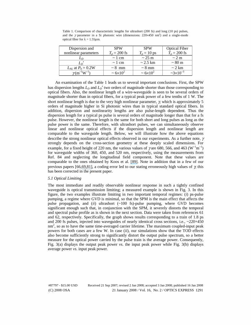
Table 1. Comparison of characteristic lengths for ultrashort (200 fs) and long (10 ps) pulses, and the γ parameter in a Si photonic wire (dimensions: 220×450 nm2) and a single-mode optical fiber for λ = 1.55μm.
Dispersion and
nonlinear parameters SPW
Tp = 200 fs SPW
Tp = 10 ps Optical Fiber Tp = 200 fs
LD ~ 1 cm ~ 25 m ~ 2 m LD′ ~ 1 cm ~ 2.5 km ~ 80 m
LNL at P0 = 0.2W ~ 8 mm ~ 8 mm ~ 2 km γ (m−1W−1) ~ 6×10² ~ 6×10² ~3×10⁻³
An examination of the Table 1 leads us to several important conclusions. First, the SPW
has dispersion lengths LD and LD′ two orders of magnitude shorter than those corresponding to optical fibers. Also, the nonlinear length of a wire-waveguide is seen to be several orders of magnitude shorter than in optical fibers, for a typical peak power of a few tenths of 1 W. The short nonlinear length is due to the very high nonlinear parameter, γ, which is approximately 5 orders of magnitude higher in Si photonic wires than in typical standard optical fibers. In addition, dispersion and nonlinearity lengths are also pulse-length dependent. Thus the dispersion length for a typical ps pulse is several orders of magnitude longer than that for a fs pulse. However, the nonlinear length is the same for both short and long pulses as long as the pulse power is the same. Therefore, with ultrashort pulses, we can simultaneously observe linear and nonlinear optical effects if the dispersion length and nonlinear length are comparable to the waveguide length. Below, we will illustrate how the above equations describe the strong nonlinear optical effects observed in our experiments. As a further note, γ strongly depends on the cross-section geometry at these deeply scaled dimensions. For example, for a fixed height of 220 nm, the various values of γ are 680, 566, and 463 (W−1m−1) for waveguide widths of 360, 450, and 520 nm, respectively, using the measurements from Ref. 84 and neglecting the longitudinal field component. Note that these values are comparable to the ones obtained by Koos et al. [89]. Note in addition that in a few of our previous papers [66,69,81], a coding error led to our stating erroneously high values of γ; this has been corrected in the present paper.
5.1 Optical Limiting
The most immediate and readily observable nonlinear response in such a tightly confined waveguide is optical transmission limiting; a measured example is shown in Fig. 3. In this figure, the two examples illustrate limiting in two important temporal regimes: (i) ps-pulse pumping, a regime where GVD is minimal, so that the SPM is the main effect that affects the pulse propagation, and (ii) ultrashort (~100 fs)-pulse pumping, where GVD becomes significant enough such that, in conjunction with the SPM, it severely distorts the temporal and spectral pulse profile as is shown in the next section. Data were taken from references 61 and 62, respectively. Specifically, the graph shows results corresponding to a train of 1.8 ps and 200 fs pulses, injected into waveguides of nearly identical cross sections, i.e., ~220×450 nm2, so as to have the same time-averaged carrier lifetime. The maximum coupled-input peak powers for both cases are a few W. In case (ii), our simulations show that the TOD effects also become sufficiently strong to significantly distort the output pulse spectrum, so a better measure for the optical power carried by the pulse train is the average power. Consequently, Fig. 3(a) displays the output peak power vs. the input peak power while Fig. 3(b) displays average power vs. input peak power.
#87797 - $15.00 USD Received 21 Sep 2007; revised 2 Jan 2008; accepted 3 Jan 2008; published 16 Jan 2008
(C) 2008 OSA 21 January 2008 / Vol. 16, No. 2 / OPTICS EXPRESS 1291
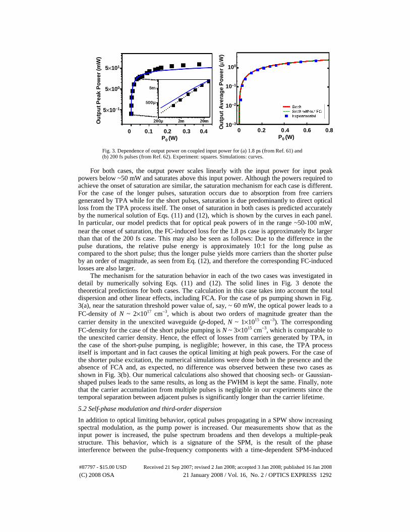
Fig. 3. Dependence of output power on coupled input power for (a) 1.8 ps (from Ref. 61) and (b) 200 fs pulses (from Ref. 62). Experiment: squares. Simulations: curves.
For both cases, the output power scales linearly with the input power for input peak
powers below ~50 mW and saturates above this input power. Although the powers required to achieve the onset of saturation are similar, the saturation mechanism for each case is different. For the case of the longer pulses, saturation occurs due to absorption from free carriers generated by TPA while for the short pulses, saturation is due predominantly to direct optical loss from the TPA process itself. The onset of saturation in both cases is predicted accurately by the numerical solution of Eqs. (11) and (12), which is shown by the curves in each panel. In particular, our model predicts that for optical peak powers of in the range ~50-100 mW, near the onset of saturation, the FC-induced loss for the 1.8 ps case is approximately 8× larger than that of the 200 fs case. This may also be seen as follows: Due to the difference in the pulse durations, the relative pulse energy is approximately 10:1 for the long pulse as compared to the short pulse; thus the longer pulse yields more carriers than the shorter pulse by an order of magnitude, as seen from Eq. (12), and therefore the corresponding FC-induced losses are also larger.
The mechanism for the saturation behavior in each of the two cases was investigated in detail by numerically solving Eqs. (11) and (12). The solid lines in Fig. 3 denote the theoretical predictions for both cases. The calculation in this case takes into account the total dispersion and other linear effects, including FCA. For the case of ps pumping shown in Fig. 3(a), near the saturation threshold power value of, say, ~ 60 mW, the optical power leads to a FC-density of N ~ 2×1017 cm−3, which is about two orders of magnitude greater than the carrier density in the unexcited waveguide (p-doped, N ~ 1×1015 cm−3). The corresponding FC-density for the case of the short pulse pumping is N ~ 3×1015 cm−3, which is comparable to the unexcited carrier density. Hence, the effect of losses from carriers generated by TPA, in the case of the short-pulse pumping, is negligible; however, in this case, the TPA process itself is important and in fact causes the optical limiting at high peak powers. For the case of the shorter pulse excitation, the numerical simulations were done both in the presence and the absence of FCA and, as expected, no difference was observed between these two cases as shown in Fig. 3(b). Our numerical calculations also showed that choosing sech- or Gaussian-shaped pulses leads to the same results, as long as the FWHM is kept the same. Finally, note that the carrier accumulation from multiple pulses is negligible in our experiments since the temporal separation between adjacent pulses is significantly longer than the carrier lifetime.
5.2 Self-phase modulation and third-order dispersion
In addition to optical limiting behavior, optical pulses propagating in a SPW show increasing spectral modulation, as the pump power is increased. Our measurements show that as the input power is increased, the pulse spectrum broadens and then develops a multiple-peak structure. This behavior, which is a signature of the SPM, is the result of the phase interference between the pulse-frequency components with a time-dependent SPM-induced
Ou
tpu
t Pea
k P
ow
er (m
W)
5×101
5×100
5×10⁻¹
0 0.2 0.4 0.6 0.8P0 (W)
100
10–1
10–2
10–3
Ou
tpu
t A
vera
ge
Po
wer
(μW
)
0 0.1 0.2 0.3 0.4P0 (W)
Ou
tpu
t Pea
k P
ow
er (m
W)
5×101
5×100
5×10⁻¹
0 0.2 0.4 0.6 0.8P0 (W)
100
10–1
10–2
10–3
Ou
tpu
t A
vera
ge
Po
wer
(μW
)
0 0.1 0.2 0.3 0.4P0 (W)
#87797 - $15.00 USD Received 21 Sep 2007; revised 2 Jan 2008; accepted 3 Jan 2008; published 16 Jan 2008
(C) 2008 OSA 21 January 2008 / Vol. 16, No. 2 / OPTICS EXPRESS 1292

frequency chirp. We find through our simulations that in Si wires, the SPM can be strongly influenced by the optical properties of the medium including TPA, TPA-induced free carriers, and TOD. Because of the small energy carried by an ultrashort pulse, the effect of FCA is generally less severe if not absent, as observed for the case of optical limiting above. Moreover, the laser repetition rate can play an important role if the lifetime of the carriers is longer or comparable with the interpulse temporal separation, since in this case, the carriers will accumulate over time and may become a source of loss as well as a source of phase shift. Accumulation is important if the carriers have a sufficiently long lifetime, as is typical for unbiased large cross-section waveguides, i.e., A0 > 1 μm2.
Fig. 4. Experimental observation of SPM with (a) 1.8 ps pulses (figure from Ref. 61) (b) 200 fs pulses (data from Ref. 62).
Figure 4 illustrates the spectral broadening of ps- and fs-pulses upon propagation in SPWs
with similar dimensions. One striking behavior, which is shown in Fig. 4(b), is the strong modulation of the spectra, as well as a more pronounced asymmetry of the pulse profile, which increases with the input power. Spectral asymmetry, in general, may result from FCA, TOD, or the initial input-pulse asymmetry but our simulations indicate that TOD is the dominant effect for the short-pulse data shown in Fig. 4(b). In optical fibers, SPM-induced spectral broadening of ps-pulses is normally symmetric around the center frequency and similarly, for propagation of such pulses in SPWs, only minimal asymmetry is observed [88]. For much larger Si waveguides, carrier lifetimes are longer and the resulting FCA can cause spectral asymmetry [57]. As we have discussed above, while FCA may become a significant effect for ps or longer pulses, it is greatly reduced for fs pulses, as is the case for the optical limiting experiments above. Hence, for the case of the ultrashort-pulse pumping in Si wires, TOD becomes the dominant factor responsible for the spectral asymmetry seen in Fig. 4(b). Our numerical simulations, as discussed in the next subsection, further support this observation.
Our theoretical model accurately describes the spectral changes in the output pulse induced by the SPM effect. Figure 5 shows the experimental and simulation results using hyperbolic-secant pulse shape for the 200 fs pulse; the numbers 1-8 indicate a series of smaller features or peaks. The agreement between data and simulations is excellent. The output spectrum obtained with the hyperbolic-secant pulse shape agrees with the experimental data in Fig. 5(a), particularly with regard to the output spectral shape and the spectral shift of the split peaks. Note also the spectral peak at 1590 nm, peak 7; this feature is not a simple SPM peak but rather we attribute this feature to the effects of soliton physics. This point will be discussed in the next subsection. We have also performed simulation using Gaussian-shaped input pulses. The output spectrum corresponding to the Gaussian input contains less spectral
γP0 = 8.0 (cm–1)3.6 (cm–1)1.4 (cm–1)0.3 (cm–1)0.2 (cm–1)
γ P0 = 56.3 (cm–1)33.8 (cm–1)11.3 (cm–1)
1.1 (cm–1)
b)
γP0 = 8.0 (cm–1)3.6 (cm–1)1.4 (cm–1)0.3 (cm–1)0.2 (cm–1)
γP0 = 8.0 (cm–1)3.6 (cm–1)1.4 (cm–1)0.3 (cm–1)0.2 (cm–1)
γ P0 = 56.3 (cm–1)33.8 (cm–1)11.3 (cm–1)
1.1 (cm–1)
b) γ P0 = 56.3 (cm–1)33.8 (cm–1)11.3 (cm–1)
1.1 (cm–1)
b)
#87797 - $15.00 USD Received 21 Sep 2007; revised 2 Jan 2008; accepted 3 Jan 2008; published 16 Jan 2008
(C) 2008 OSA 21 January 2008 / Vol. 16, No. 2 / OPTICS EXPRESS 1293

features, but the imbalance between the left and right peaks is closer to the experimental result. This demonstrates some degree of sensitivity of the output spectrum to input pulse shape.
Fig 5. Measured and experimental transmission through a Si photonic wire waveguide with γP0
= 56.3 cm−1. Left panel: measured spectra (brown). Right panel: simulation using hyperbolic secant input pulse (red). Blue curves on both panels correspond to γP0 = 1.1 cm−1 (with sech input pulse for simulation). Dashed line: OSA noise floor. The numbers are shown to illustrate the correspondence between experiment and simulation. From Ref. 62.
At pump peak powers approaching 1 W, (or correspondingly 0Pγ ≈ 22.5 cm−1 for a 220 ×
450 nm2 cross-section waveguide), intensities of ~ 1GW/cm2 can be attained inside the waveguide, which give rise to the nonlinear effects discussed above. At higher powers, the level of the light intensity is sufficient to generate supercontinuum arising from a cascade of nonlinear effects. In addition, the efficiency of supercontinuum generation is enhanced if the input pulse is launched in the anomalous dispersion regime, near the ZGVD point so that the optical dispersion is small and, thus, does not reduce the strength of the nonlinear effects due to temporal pulse spreading. Recently, we have experimentally demonstrated supercontinuum generation in a 4.7-mm-long SPW waveguide upon propagation of ultrashort, ~100 fs, 1.3-μm-wavelength optical pulses near its ZGVD wavelength [69].
5.3 Soliton generation
As indicated above, soliton radiation and its effects can be readily seen in SPW. The work of Hsieh et al. [62] described below constitutes the first observation of soliton effects in silicon photonic wires, supported strongly by numerical simulations. Recently, in a related measurement, Zhang et al. have also observed soliton propagation in larger Si rib-waveguides having dimensions of 860×400 nm2
and an etching depth of 300 nm [90]. In a recent theoretical study, it has been demonstrated that fission of higher-order solitons in Si waveguides may generate supercontinuum [91], an important functionality. As in optical fibers, soliton radiation is generated during the propagation of soliton pulses, which are perturbed by higher-order dispersive effects, namely TOD [88]. However, in the case of Si wires the effective nonlinear coefficient is ~105 larger and thus soliton effects are seen in wires of only millimeters in length. Thus, in addition to SPM frequency broadening, Fig. 5 shows a spectral feature, which is attributable to soliton radiation. The evolution of the spectra with power is shown in Fig. 6, which displays both experimental and numerical simulation results. This figure shows that as the input power increases, a spectral feature develops near 1590 nm for 0Pγ = 45 cm−1 (brown curve). There are several reasons why the emergence of this spectral feature can be viewed as the result of the influence of the TOD on the soliton propagation: (1) the soliton number is Nsoliton = (LD/LNL)1/2 = 6.6, i.e., the pulse propagation is in the soliton regime; (2) the pulse propagation is in the anomalous GVD regime, a key requirement for the soliton existence; and (3) the location of this peak remains constant over a
1
2
3
4
5
6
7
8
1
2
34
5
6 7
8
1
2
3
4
5
6
7
81
2
3
4
5
6
7
8
1
2
34
5
6 7
8
1
2
34
5
6 7
8
1
2
3
4
5
6
7
8
1
2
34
5
6 7
8
1
2
3
4
5
6
7
81
2
3
4
5
6
7
8
1
2
34
5
6 7
8
1
2
34
5
6 7
8
#87797 - $15.00 USD Received 21 Sep 2007; revised 2 Jan 2008; accepted 3 Jan 2008; published 16 Jan 2008
(C) 2008 OSA 21 January 2008 / Vol. 16, No. 2 / OPTICS EXPRESS 1294

large range of powers. In addition, since the peak is significantly shifted from the main SPM features, it cannot be attributed to SPM effects.
The location of this peak can also be used to determine the waveguide TOD coefficient, by using a similar procedure to that used to measure β3 of optical fibers [92]. In particular, by using the position of this spectral peak we can infer the value of β3 by using the relation β3 = 3|β2|Τ0 /ωr, where ωr is the normalized angular frequency separation between the center frequency and the soliton feature [93,94]. Note that this relation does not account for the dependence of ωr on dispersion coefficients beyond the third-order, as well as the power dependence of the waveguide dispersion. These effects are small and are commonly neglected. In addition, we used the pulse width T0 in the relation that determines the frequency of resonantly emitted radiation. In a more rigorous approach, which is beyond the scope of this review, one should first determine the soliton content of the input pulse, use a perturbative approach based on, e.g., the inverse scattering transform to determine the dynamics of the corresponding solitons, and then use the width of the first emitted soliton. As an alternative, we can determine β3 by fitting the numerically found spectra to the experimental data. Thus we solve Eqs. (11) and (12) for several values of β3 in the vicinity of the estimated value until the various features of the spectrum shown in Fig. 5(a), such as the peaks and dips, are reproduced. This method yields β3 = –0.73 ± 0.05 ps3/m.
Fig 6. Evolution of spectra at different excitation conditions γP0 = 1.1, 11.3, 33.8, 45.0 cm−1 (bottom to top) spectra. Note also the evolution of soliton radiation (dashed line) at 1590 nm.
5.4 Cross-phase modulation
As we have shown above, SPM alters the phase of the optical pulse and as a result this effect can have important practical applications. Increased design flexibility can be achieved by controlling the phase of a pulse at one wavelength with a second, co-propagating pulse, at a different wavelength, i.e., cross phase modulation. Cross-phase modulation is also described by our general coupled-mode theory by means of Eqs. (1)-(3). We illustrate XPM in SPW by using two pulses of different wavelengths that co-propagate in the same waveguide, as described in the experiments above and using the data from Ref. 66. These two pulses are derived using an ultrafast mode-locked Er-doped fiber-laser having a pulse repetition rate of 37 MHz and a bandwidth of 80 nm. After passing through a beam splitter and bandpass filters, this laser beam is split into the pump and probe beams, with center wavelengths at λp = 1527
#87797 - $15.00 USD Received 21 Sep 2007; revised 2 Jan 2008; accepted 3 Jan 2008; published 16 Jan 2008
(C) 2008 OSA 21 January 2008 / Vol. 16, No. 2 / OPTICS EXPRESS 1295
nm and λs = 1590 nm, respectively. The pulse width and bandwidth of the resulting pulses are approximately 200 fs and 15 nm, respectively. Both pulses are free-space coupled into the waveguide and are polarized along the direction of the field of the TE waveguide mode. The output was collected by a tapered fiber and sent to an OSA. Free-space coupling, rather than tapered fiber coupling, is employed to rule out SPM and XPM in the input fiber.
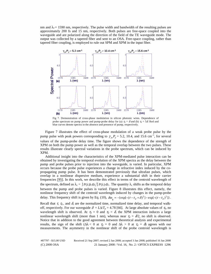
Fig 7. Demonstration of cross-phase modulation in silicon photonic wires. Dependence of probe spectrum on pump power and pump-probe delay for (a) τd = δ and (b) τd = 5δ. Red and blue curves denote spectra in the absence and presence of pump, respectively.
Figure 7 illustrates the effect of cross-phase modulation of a weak probe pulse by the
pump pulse with peak powers corresponding to pps Pγ = 5.2, 10.4, and 15.6 cm−1, for several
values of the pump-probe delay time. The figure shows the dependence of the strength of XPM on both the pump power as well as the temporal overlap between the two pulses. These results illustrate clearly spectral variations in the probe spectrum, which can be induced by XPM.
Additional insight into the characteristics of the XPM-mediated pulse interaction can be obtained by investigating the temporal evolution of the XPM spectra as the delay between the pump and probe pulses prior to injection into the waveguide, is varied. In particular, XPM occurs because the probe pulse experiences a change in refractive index induced by the co-propagating pump pulse. It has been demonstrated previously that ultrafast pulses, which overlap in a nonlinear dispersive medium, experience a substantial shift in their carrier frequencies [95]. In this work, we describe this effect in terms of the centroid wavelength of the spectrum, defined as λc = dλ)λ(dλλ)λ( ∫∫ PP . The quantity λc shifts as the temporal delay between the pump and probe pulses is varied. Figure 8 illustrates this effect, namely, the nonlinear frequency shift of the centroid wavelength induced by changes in the pump-probe delay. This frequency shift is given by Eq. (10), ]})(exp[])({exp[ 22
dds ττδττδω −−−+−−−∝ .
Recall that τ, τd , and δ, are the normalized time, normalized time delay, and temporal walk-off, respectively. For our waveguide δ = LΔ/Tp = 4.78 [66]. At large absolute values of τd, no wavelength shift is observed. At τd = 0 and τd = δ, the XPM interaction induces a large nonlinear wavelength shift (more than 1 nm), whereas near τd = δ/2, no shift is observed. Notice that in addition to the good agreement between theoretical analysis and experimental results, the sign of the shift (Δλ < 0 at τd = 0 and Δλ > 0 at τd = δ) agrees with our measurements. The asymmetry in the nonlinear shift of the probe centroid wavelength is
1570 1585 1600
0.5
1
1570 1585 1600
0.5
1
1570 1585 1600
0.5
1
1570 1585 1600
0.5
1
1570 1585 1600
0.5
1
1570 1585 1600
0.5
1
λ (nm) λ (nm) λ (nm)
Spe
ctra
l Pow
er
(a)
λ (nm) λ (nm) λ (nm)(b)
γ psPp ≈ 5.2 cm-1 γ psPp ≈ 10.4 cm-1 γ psPp ≈ 15.6 cm-1
1570 1585 1600
0.5
1
1570 1585 1600
0.5
1
1570 1585 1600
0.5
1
1570 1585 1600
0.5
1
1570 1585 1600
0.5
1
1570 1585 1600
0.5
1
λ (nm) λ (nm) λ (nm)
Spe
ctra
l Pow
er
(a)
λ (nm) λ (nm) λ (nm)(b)
γ psPp ≈ 5.2 cm-1 γ psPp ≈ 10.4 cm-1 γ psPp ≈ 15.6 cm-1
#87797 - $15.00 USD Received 21 Sep 2007; revised 2 Jan 2008; accepted 3 Jan 2008; published 16 Jan 2008
(C) 2008 OSA 21 January 2008 / Vol. 16, No. 2 / OPTICS EXPRESS 1296

explained by the fact that in the case in which τd = 0 the pump-probe interaction takes place mostly near the input facet of the waveguide whereas when τd = δ the pump interacts with the probe mostly near the output of the SPW, i.e., after the pump has lost part of its optical power due to intrinsic and TPA losses. Note further that the peak near τd = 0 is narrower than the one near τd = δ, a behavior that is attributable to the slight temporal broadening of both the pump and probe pulses due to frequency dispersion. Although the temporal broadening is small, the numerical simulation shown in Fig. 8 predicts a small difference in the width of the two lobes.
As suggested above, a potential application of XPM is nonlinear frequency (wavelength) shifting, which has important use, e.g., for providing wavelength-channel dropping functionality. As shown above in Eq. (10), the amount of wavelength shift scales with the pump power. For example, Dekker et al. have demonstrated XPM-induced wavelength shifts of as much as >10 nm, which are comparable to the spectral width of the input probe pulses [65]. Therefore, a XPM-induced frequency shift can be employed in designing ultra-fast all-optical switches, which can be used to switch-off pulses as short as a few hundred femtoseconds.
Fig. 8. Experimental (red) and numerical simulation (blue) results showing the dependence of cross-phase modulation on the normalized time delay. The center wavelength of the probe is ~1590 nm.
5.5 Modulation Instability in Si photonic wires
A critical functionality that SPWs can readily provide is tunable optical gain at one or more frequencies. Recently, Panoiu et al. proposed an all-optical scheme that allows one to achieve strong optical gain in a millimeter-long SPW [96]. Specifically they numerically demonstrated that two optical continuous-wave (cw) beams that copropagate in a SPW could generate a strong modulation instability (MI). MI is manifested within a propagation distance of just a few millimeters. The MI gain depends on the power of the optical waves so that it can be optically tuned, and it reaches its maximum value when both waves experience anomalous GVD. As a result of the MI, the optical waves develop deep subpicosecond modulations. These findings could play an important role in designing on-chip sources of ultrashort optical pulses. We present here two cases: case A, in which one wave propagates in the normal GVD region, and the other one experiences anomalous GVD; and case B, in which both waves propagate in the anomalous GVD region.
The SPW has width w = 360 nm and height h = 220 nm, dimensions for which the ZGVD point is at λ0 = 1550 nm. It should be noted that λ0 belongs to a second set of ZGVD wavelengths not shown in Fig. 2. The dynamics of the two optical waves propagating in the SPW is governed by the system of Eqs. (1)-(3). To investigate the MI of two optical waves whose propagation is described by this system, we first determine its steady-state (cw) solutions, i.e., z-independent solutions, and then analyze the linear dynamics of small
#87797 - $15.00 USD Received 21 Sep 2007; revised 2 Jan 2008; accepted 3 Jan 2008; published 16 Jan 2008
(C) 2008 OSA 21 January 2008 / Vol. 16, No. 2 / OPTICS EXPRESS 1297

perturbations of the cw solutions [88,97-102]. Thus, simple calculations show that, if we neglect the linear and nonlinear losses, the MI gain spectrum defined by G(Ω)=2 Im[Λ(Ω)] is determined by the equation
( )[ ] ( )[ ] 42
,
2
, // Ω=−Ω−Λ−Ω−Λ ηρρ ssgppg vv (15)
where Ω and Λ are the frequency and wavevector of the modulation, respectively, η = 4γpsγspβ2pβ2sPpPs, ρp,s = β2p,sΩ2(γp,sPp,s+β2p,sΩ2/4). Now consider the MI gain in two cases. In case A, the pump beam propagates in the normal GVD region, λp = 1625.3 nm, whereas in case B it experiences anomalous GVD, λp=1400 nm. In both cases the signal beam propagates in the anomalous GVD region, at λs=1450 nm. In case A, we chose the two wavelengths so that the waves have the same group velocity, and thus there is no temporal walk-off, whereas in case B the walk-off parameter is Δ = |1/vg,p−1/vg,s| = 86.3 ps/m. By using Eq. (15), we determined the dependence of the gain spectra versus the pump power Pp, for a signal power Ps = 200 mW in case A, and Ps = 40 mW in case B. The results, presented in Fig. 9, show that in both cases the co-propagating waves experience strong MI, with a bandwidth of the gain spectrum of 10 THz. For comparison, the Raman gain bandwidth of silicon is in excess of 0.1 THz [29]. Potentially comparable gain bandwidth is expected in broadband FWM when the guide has anomalous dispersion; gain bandwidths of a few THz have been demonstrated experimentally [53].
Note that although the powers Pp, Ps are smaller in case B, a larger MI gain is observed in this case, namely when both waves experience anomalous GVD. However, note that in both cases the MI gain is 102-103 times as large as the MI gain achievable in optical fibers, for similar values of the optical powers. This is because the γ parameters, which determine the strength of the MI gain, are much larger for SPWs as compared with that of optical fibers. In addition, the frequency corresponding to the maximum MI gain can be tuned by changing the power of the interacting waves, so our results suggest that MI can be employed to design on-chip optical amplifiers that provide tunable optical gain.
Fig. 9. Calculated modulation instability gain spectra for (a) case A and (b) case B as described in the text.
5.6 Pulse Compression in Si photonic wires
Pulse compression is a particularly interesting application of cross phase modulation since it makes use of both the dispersion-engineered properties of the waveguide and the strong nonlinearity of silicon. Pulse compression is an important functionality, which can potentially be achieved in millimeter-long devices implemented in the SOI platform. Recently, Chen et al. demonstrated theoretically that dispersion engineering in conjunction with SPM and TOD can be used to compress pulses [81]; in addition, Tien et al. experimentally demonstrated pulse compression in Si waveguides, but using FCA [103]. Below we show that XPM can provide an optically controlled pulse-compression process. In this approach, a strong pump modifies the phase experienced by the probe beam and thus generates additional bandwidth that can support shorter pulses. This requires that the pump-probe interaction length be equal to or larger than the waveguide length, and that a weak signal (probe) beam experience anomalous dispersion regime. The first requirement implies that the group velocity of the two pulses is
#87797 - $15.00 USD Received 21 Sep 2007; revised 2 Jan 2008; accepted 3 Jan 2008; published 16 Jan 2008
(C) 2008 OSA 21 January 2008 / Vol. 16, No. 2 / OPTICS EXPRESS 1298

equal or close enough so that the probe pulse interacts with the pump over the entire length of the waveguide. After the probe acquires sufficient bandwidth via XPM interaction, it is then compressed temporally as the probe propagates in the anomalous GVD regime. In the numerical simulations, shown in Fig. 10, the waveguide is dispersion engineered such that the probe and pump pulses have the same group velocity but have negative and positive GVD, respectively. The figure shows that SPW enables compression in particularly short guided wavelength; namely, after a propagation length of just 0.8 mm the probe pulse is compressed by a factor of ~5.
Fig. 10. Simulation of pulse compression via cross-phase modulation. Signal (left panel) and pump (right panel) field envelopes vs. time and propagation distance. The temporal width is 200 fs for both the pump and signal pulses. Here γpsPp ≈100 cm−1 for the pump, with a center frequency of 1625 nm. For the signal Ps << Pp and the center frequency of it is 1451 nm. Insets: initial and final pulse envelopes. The waveguide dimensions are w×h = 360 × 220 nm2.
6. Conclusion
In this article, we have presented a review of our previous and current work on linear and nonlinear optical effects in Si photonic wires. In particular we have demonstrated experimental and theoretical studies of dispersion engineering and of optical nonlinearity with particular emphasis on SPM and XPM from ps and fs pulses in Si wires. As a consequence of dispersion engineering, such photonic wires can be designed to operate over a wide range of GVD values at telecom wavelengths. By operating in a regime where the waveguide, characteristic dispersion, and nonlinear lengths are comparable to each other, we have been able to probe the complex interplay among all these effects at low peak powers of the order of a few hundreds of mW and with waveguide lengths of a few mm. In addition, a further reduction in the Si wire cross-sectional dimension provides further scaling down of the length × power required for nonlinear optical functionalities, which arises from both the reduced area and reduced group velocity of the optical waves. The low threshold powers for phase-changing effects in Si photonic wires make them potential candidates for various functional nonlinear optical devices in an integrated platform.
Acknowledgments
This research was supported by the DoD STTR, Contract No. FA9550-05-C-1954, and by the AFOSR Grant FA9550-05-1-0428. The IBM part of this work as supported by Grant No. N00014-07-C-0105 ONR/DARPA. We thank Alexander Wirthmüller for useful and illuminating discussions.
#87797 - $15.00 USD Received 21 Sep 2007; revised 2 Jan 2008; accepted 3 Jan 2008; published 16 Jan 2008
(C) 2008 OSA 21 January 2008 / Vol. 16, No. 2 / OPTICS EXPRESS 1299
Related Documents

![Tuning of the Optical Properties in Photonic Crystals Made ... · optical devices. These structures, referred to as photonic crystals [3–11], are characterized by an unusual dispersion](https://static.cupdf.com/doc/110x72/612fc90c1ecc51586943aca6/tuning-of-the-optical-properties-in-photonic-crystals-made-optical-devices.jpg)


