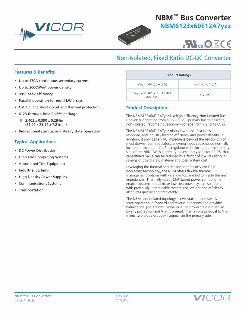
NBM ™ Bus Converter NBM6123x60E12A7yzz NBM™ Bus Converter Rev 1.8 Page 1 of 26 11/2017 Non-Isolated, Fixed Ratio DC-DC Converter S NRTL C US C US ® Features & Benefits • Up to 170A continuous secondary current • Up to 3000W/in 3 power density • 98% peak efficiency • Parallel operation for multi-kW arrays • OV, OC, UV, short circuit and thermal protection • 6123 through-hole ChiP™ package ■ 2.402 x 0.990 x 0.284in (61.00 x 25.14 x 7.21mm) • Bidirectional start up and steady state operation Typical Applications • DC Power Distribution • High End Computing Systems • Automated Test Equipment • Industrial Systems • High Density Power Supplies • Communications Systems • Transportation Product Description The NBM6123x60E12A7yzz is a high efficiency Non Isolated Bus Converter operating from a 36 – 60V DC primary bus to deliver a non-isolated, ratiometric secondary voltage from 7.2 to 12.0V DC . The NBM6123x60E12A7yzz offers low noise, fast transient response, and industry leading efficiency and power density. In addition, it provides an AC impedance beyond the bandwidth of most downstream regulators, allowing input capacitance normally located at the input of a PoL regulator to be located at the primary side of the NBM. With a primary to secondary K factor of 1/5, that capacitance value can be reduced by a factor of 25x, resulting in savings of board area, material and total system cost. Leveraging the thermal and density benefits of Vicor ChiP packaging technology, the NBM offers flexible thermal management options with very low top and bottom side thermal impedances. Thermally-adept ChiP-based power components enable customers to achieve low cost power system solutions with previously unattainable system size, weight and efficiency attributes quickly and predictably. The NBM non-isolated topology allows start up and steady state operation in forward and reverse directions and provides bidirectional protections. However if the power train is disabled by any protection and V SEC is present, then a voltage equal to V SEC minus two diode drops will appear on the primary side. Product Ratings V PRI = 54V (36 – 60V) I SEC = up to 170A V SEC = 10.8V (7.2 – 12.0V) (NO LOAD) K = 1/5

Welcome message from author
This document is posted to help you gain knowledge. Please leave a comment to let me know what you think about it! Share it to your friends and learn new things together.
Transcript
NBM™ Bus ConverterNBM6123x60E12A7yzz
NBM™ Bus Converter Rev 1.8Page 1 of 26 11/2017
Non-Isolated, Fixed Ratio DC-DC Converter
S
NRTLC USC US®
Features & Benefits
• Up to 170A continuous secondary current
• Up to 3000W/in3 power density
• 98% peak efficiency
• Parallel operation for multi-kW arrays
• OV, OC, UV, short circuit and thermal protection
• 6123 through-hole ChiP™ package
■■ 2.402 x 0.990 x 0.284in (61.00 x 25.14 x 7.21mm)
• Bidirectional start up and steady state operation
Typical Applications
• DC Power Distribution
• High End Computing Systems
• Automated Test Equipment
• Industrial Systems
• High Density Power Supplies
• Communications Systems
• Transportation
Product Description
The NBM6123x60E12A7yzz is a high efficiency Non Isolated Bus Converter operating from a 36 – 60VDC primary bus to deliver a non-isolated, ratiometric secondary voltage from 7.2 to 12.0VDC.
The NBM6123x60E12A7yzz offers low noise, fast transient response, and industry leading efficiency and power density. In addition, it provides an AC impedance beyond the bandwidth of most downstream regulators, allowing input capacitance normally located at the input of a PoL regulator to be located at the primary side of the NBM. With a primary to secondary K factor of 1/5, that capacitance value can be reduced by a factor of 25x, resulting in savings of board area, material and total system cost.
Leveraging the thermal and density benefits of Vicor ChiP packaging technology, the NBM offers flexible thermal management options with very low top and bottom side thermal impedances. Thermally-adept ChiP-based power components enable customers to achieve low cost power system solutions with previously unattainable system size, weight and efficiency attributes quickly and predictably.
The NBM non-isolated topology allows start up and steady state operation in forward and reverse directions and provides bidirectional protections. However if the power train is disabled by any protection and VSEC is present, then a voltage equal to VSEC minus two diode drops will appear on the primary side.
Product Ratings
VPRI = 54V (36 – 60V) ISEC = up to 170A
VSEC = 10.8V (7.2 – 12.0V)(no load)
K = 1/5

NBM™ Bus Converter Rev 1.8Page 2 of 26 11/2017
NBM6123x60E12A7yzz
NBM
VAUX
EN
+VPRI
SGND
+VSEC
VPRI
enable/disableswitch
FUSE
PRIMARY SECONDARY
SOURCE_RTN
CI_NBM_ELEC
TM
POL
PGND
Typical Applications
NBM6123x60E12A7yzz + Point of Load
NBM™ Bus Converter Rev 1.8Page 3 of 26 11/2017
NBM6123x60E12A7yzz
1 2
A
B
C
D
E
F
G
H
+VPRI
+VSEC
TOP VIEW
6123 ChiP Package
I
PGND1
PGND1
+VSEC
+VSEC
PGND1
+VSEC
PGND1
+VPRI J
+VPRI K
+VPRI L
A’
B’
C’
D’
E’
F’
G’
H’
I’
J’
K’
L’
+VSEC
PGND2
PGND2
+VSEC
+VSEC
PGND2
+VSEC
PGND2
SGND
TM
EN
VAUX
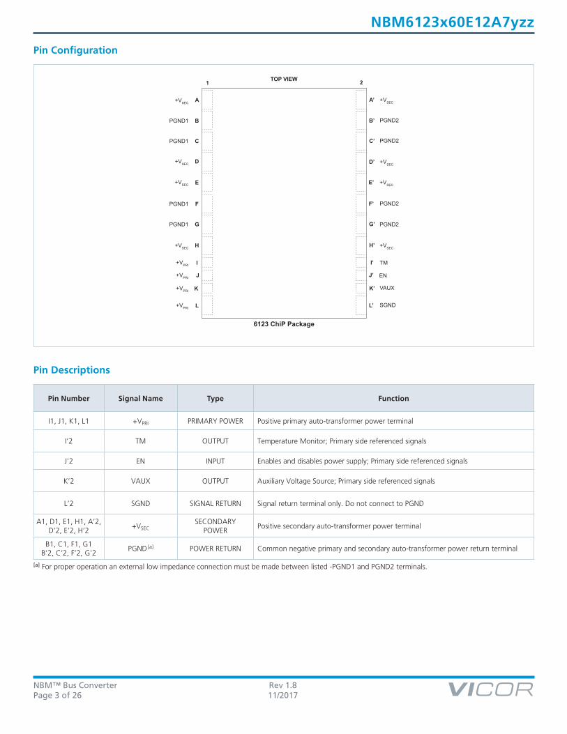
Pin Configuration
Pin Descriptions
Pin Number Signal Name Type Function
I1, J1, K1, L1 +VPRI PRIMARY POWER Positive primary auto-transformer power terminal
I’2 TM OUTPUT Temperature Monitor; Primary side referenced signals
J’2 EN INPUT Enables and disables power supply; Primary side referenced signals
K’2 VAUX OUTPUT Auxiliary Voltage Source; Primary side referenced signals
L’2 SGND SIGNAL RETURN Signal return terminal only. Do not connect to PGND
A1, D1, E1, H1, A’2, D’2, E’2, H’2
+VSECSECONDARY
POWERPositive secondary auto-transformer power terminal
B1, C1, F1, G1B’2, C’2, F’2, G’2
PGND [a] POWER RETURN Common negative primary and secondary auto-transformer power return terminal
[a] For proper operation an external low impedance connection must be made between listed -PGND1 and PGND2 terminals.

NBM™ Bus Converter Rev 1.8Page 4 of 26 11/2017
NBM6123x60E12A7yzz
Absolute Maximum Ratings
The absolute maximum ratings below are stress ratings only. Operation at or beyond these maximum ratings can cause permanent damage to the device.
Parameter Comments Min Max Unit
+VPRI_DC to –VPRI_DC –1 80 V
VPRI_DC or VSEC_DC Slew Rate
(Operational)1 V/µs
+VSEC_DC to –VSEC_DC –1 16 V
TM to –VPRI_DC
–0.3
4.6 V
EN to –VPRI_DC 5.5 V
VAUX to –VPRI_DC 4.6 V
Standard Models
Product Function
Package Size
Package Mounting
Max Primary Input Voltage
Range Identifier
Max Secondary
Voltage
SecondaryOutput Current
Temperature Grade
Option
NBM 6123 T 60 E 12 A7 T 0R
Part Ordering Information
All products shipped in JEDEC standard high profile (0.400” thick) trays (JEDEC Publication 95, Design Guide 4.10).
Product Function
Package Size
Package Mounting
Max Primary Input Voltage
Range Identifier
Max Secondary
Voltage
SecondaryOutput Current
Temperature Grade
Option
NBM 6123 x 60 E 12 A7 y zz
Non-isolated Bus Converter
Module
61 = L 23 = W
T = TH
S = SMT60V 36 – 60V
12VNo Load
170AT = –40°C – 125°C
M = –55°C – 125°C
00 = Analog Ctrl
01 = PMBus Ctrl
0R = Reversible Analog Ctrl
0P = Reversible PMBus Ctrl
NBM™ Bus Converter Rev 1.8Page 5 of 26 11/2017
NBM6123x60E12A7yzz
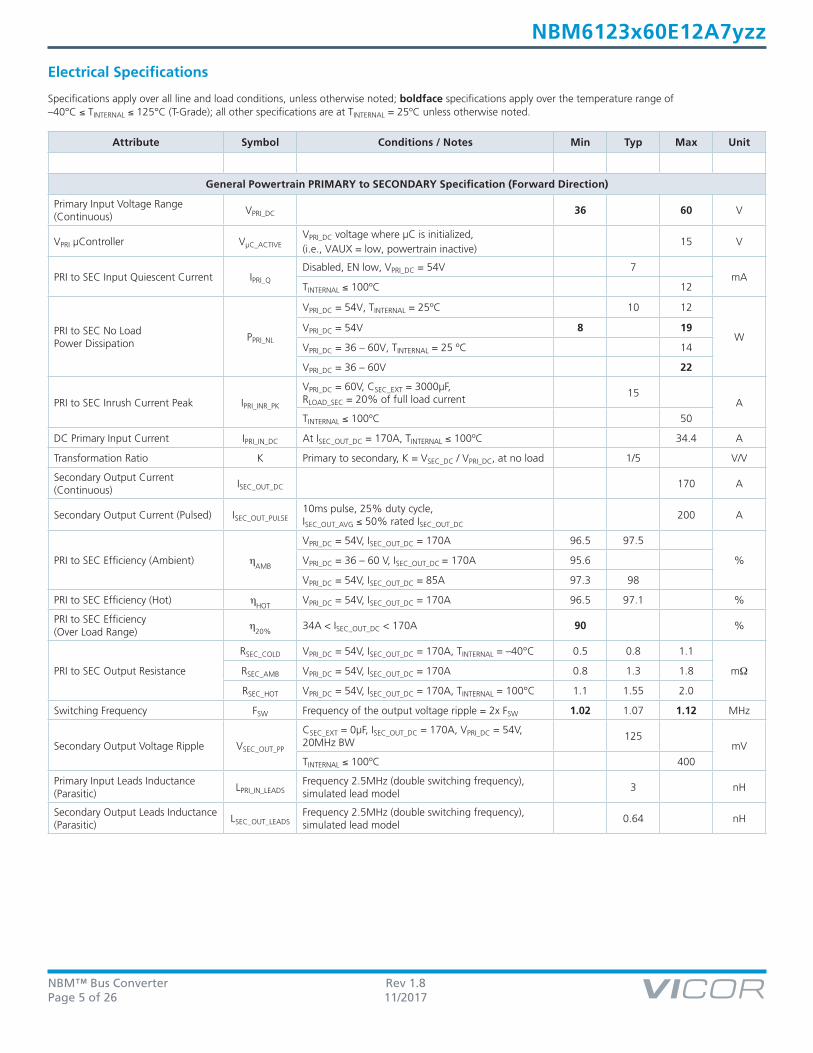
Electrical Specifications
Specifications apply over all line and load conditions, unless otherwise noted; boldface specifications apply over the temperature range of –40°C ≤ TINTERNAL ≤ 125°C (T-Grade); all other specifications are at TINTERNAL = 25ºC unless otherwise noted.
Attribute Symbol Conditions / Notes Min Typ Max Unit
General Powertrain PRIMARY to SECONDARY Specification (Forward Direction)
Primary Input Voltage Range (Continuous)
VPRI_DC 36 60 V
VPRI µController VµC_ACTIVEVPRI_DC voltage where µC is initialized, (i.e., VAUX = low, powertrain inactive)
15 V
PRI to SEC Input Quiescent Current IPRI_Q
Disabled, EN low, VPRI_DC = 54V 7mA
TINTERNAL ≤ 100ºC 12
PRI to SEC No Load Power Dissipation
PPRI_NL
VPRI_DC = 54V, TINTERNAL = 25ºC 10 12
WVPRI_DC = 54V 8 19
VPRI_DC = 36 – 60V, TINTERNAL = 25 ºC 14
VPRI_DC = 36 – 60V 22
PRI to SEC Inrush Current Peak IPRI_INR_PK
VPRI_DC = 60V, CSEC_EXT = 3000µF, RLOAD_SEC = 20% of full load current
15A
TINTERNAL ≤ 100ºC 50
DC Primary Input Current IPRI_IN_DC At ISEC_OUT_DC = 170A, TINTERNAL ≤ 100ºC 34.4 A
Transformation Ratio K Primary to secondary, K = VSEC_DC / VPRI_DC, at no load 1/5 V/V
Secondary Output Current (Continuous)
ISEC_OUT_DC 170 A
Secondary Output Current (Pulsed) ISEC_OUT_PULSE10ms pulse, 25% duty cycle, ISEC_OUT_AVG ≤ 50% rated ISEC_OUT_DC
200 A
PRI to SEC Efficiency (Ambient) ηAMB
VPRI_DC = 54V, ISEC_OUT_DC = 170A 96.5 97.5
%VPRI_DC = 36 – 60 V, ISEC_OUT_DC = 170A 95.6
VPRI_DC = 54V, ISEC_OUT_DC = 85A 97.3 98
PRI to SEC Efficiency (Hot) ηHOT
VPRI_DC = 54V, ISEC_OUT_DC = 170A 96.5 97.1 %
PRI to SEC Efficiency (Over Load Range)
η20%
34A < ISEC_OUT_DC < 170A 90 %
PRI to SEC Output Resistance
RSEC_COLD VPRI_DC = 54V, ISEC_OUT_DC = 170A, TINTERNAL = –40°C 0.5 0.8 1.1
mΩRSEC_AMB VPRI_DC = 54V, ISEC_OUT_DC = 170A 0.8 1.3 1.8
RSEC_HOT VPRI_DC = 54V, ISEC_OUT_DC = 170A, TINTERNAL = 100°C 1.1 1.55 2.0
Switching Frequency FSW Frequency of the output voltage ripple = 2x FSW 1.02 1.07 1.12 MHz
Secondary Output Voltage Ripple VSEC_OUT_PP
CSEC_EXT = 0µF, ISEC_OUT_DC = 170A, VPRI_DC = 54V, 20MHz BW
125mV
TINTERNAL ≤ 100ºC 400
Primary Input Leads Inductance (Parasitic)
LPRI_IN_LEADSFrequency 2.5MHz (double switching frequency), simulated lead model
3 nH
Secondary Output Leads Inductance (Parasitic)
LSEC_OUT_LEADSFrequency 2.5MHz (double switching frequency), simulated lead model
0.64 nH
NBM™ Bus Converter Rev 1.8Page 6 of 26 11/2017
NBM6123x60E12A7yzz
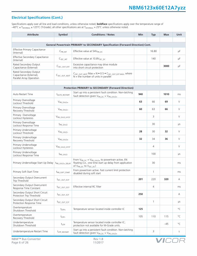
Electrical Specifications (Cont.)
Specifications apply over all line and load conditions, unless otherwise noted; boldface specifications apply over the temperature range of –40°C ≤ TINTERNAL ≤ 125°C (T-Grade); all other specifications are at TINTERNAL = 25ºC unless otherwise noted.
Attribute Symbol Conditions / Notes Min Typ Max Unit
General Powertrain PRIMARY to SECONDARY Specification (Forward Direction) Cont.
Effective Primary Capacitance (Internal)
CPRI_INT Effective value at 54VPRI_DC 16.80 µF
Effective Secondary Capacitance (Internal)
CSEC_INT Effective value at 10.8VSEC_DC 140 µF
Rated Secondary Output Capacitance (External)
CSEC_OUT_EXTExcessive capacitance may drive module into short circuit protection
3000 µF
Rated Secondary Output Capacitance (External), Parallel Array Operation
CSEC_OUT_AEXTCSEC_OUT_AEXT Max = N • 0.5 • CSEC_OUT_EXT MAX, where N = the number of units in parallel
Protection PRIMARY to SECONDARY (Forward Direction)
Auto Restart Time tAUTO_RESTARTStart up into a persistent fault condition. Non-latching fault detection given VPRI_DC > VPRI_UVLO+
940 1010 ms
Primary Overvoltage Lockout Threshold
VPRI_OVLO+ 63 66 69 V
Primary Overvoltage Recovery Threshold
VPRI_OVLO– 60 63 66 V
Primary Overvoltage Lockout Hysteresis
VPRI_OVLO_HYST 3 V
Primary Overvoltage Lockout Response Time
tPRI_OVLO 30 µs
Primary Undervoltage Lockout Threshold
VPRI_UVLO– 28 30 32 V
Primary Undervoltage Recovery Threshold
VPRI_UVLO+ 32 34 36 V
Primary Undervoltage Lockout Hysteresis
VPRI_UVLO_HYST 4 V
Primary Undervoltage Lockout Response Time
tPRI_UVLO 100 µs
Primary Undervoltage Start Up Delay tPRI_UVLO+_DELAY
From VPRI_DC = VPRI_UVLO+ to powertrain active, EN floating (i.e., one time start up delay from application of VPRI_DC to VSEC_DC)
30 ms
Primary Soft Start Time tPRI_SOFT_STARTFrom powertrain active. Fast current limit protection disabled during soft start
1 ms
Secondary Output Overcurrent Trip Threshold
ISEC_OUT_OCP 201 220 320 A
Secondary Output Overcurrent Response Time Constant
tSEC_OUT_OCP Effective internal RC filter 4 ms
Secondary Output Short Circuit Protection Trip Threshold
ISEC_OUT_SCP 250 A
Secondary Output Short Circuit Protection Response Time
tSEC_OUT_SCP 1 µs
Overtemperature Shutdown Threshold
tOTP+ Temperature sensor located inside controller IC 125 °C
Overtemperature Recovery Threshold
tOTP– 105 110 115 °C
Undertemperature Shutdown Threshold
tUTPTemperature sensor located inside controller IC; protection not available for M-Grade units.
–45 °C
Undertemperature Restart Time tUTP_RESTARTStart up into a persistent fault condition. Non-latching fault detection given VPRI_DC > VPRI_UVLO+
3 s
NBM™ Bus Converter Rev 1.8Page 7 of 26 11/2017
NBM6123x60E12A7yzz
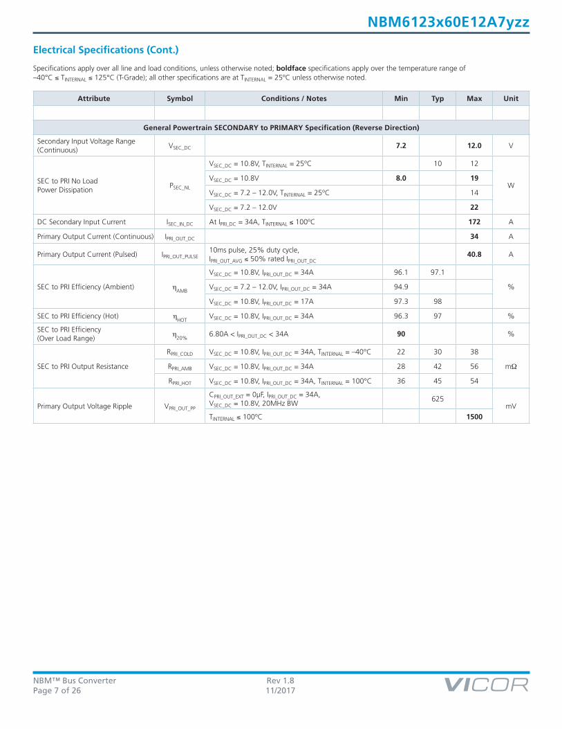
Attribute Symbol Conditions / Notes Min Typ Max Unit
General Powertrain SECONDARY to PRIMARY Specification (Reverse Direction)
Secondary Input Voltage Range (Continuous)
VSEC_DC 7.2 12.0 V
SEC to PRI No Load Power Dissipation
PSEC_NL
VSEC_DC = 10.8V, TINTERNAL = 25ºC 10 12
WVSEC_DC = 10.8V 8.0 19
VSEC_DC = 7.2 – 12.0V, TINTERNAL = 25ºC 14
VSEC_DC = 7.2 – 12.0V 22
DC Secondary Input Current ISEC_IN_DC At IPRI_DC = 34A, TINTERNAL ≤ 100ºC 172 A
Primary Output Current (Continuous) IPRI_OUT_DC 34 A
Primary Output Current (Pulsed) IPRI_OUT_PULSE10ms pulse, 25% duty cycle, IPRI_OUT_AVG ≤ 50% rated IPRI_OUT_DC
40.8 A
SEC to PRI Efficiency (Ambient) ηAMB
VSEC_DC = 10.8V, IPRI_OUT_DC = 34A 96.1 97.1
%VSEC_DC = 7.2 – 12.0V, IPRI_OUT_DC = 34A 94.9
VSEC_DC = 10.8V, IPRI_OUT_DC = 17A 97.3 98
SEC to PRI Efficiency (Hot) ηHOT
VSEC_DC = 10.8V, IPRI_OUT_DC = 34A 96.3 97 %
SEC to PRI Efficiency (Over Load Range)
η20%
6.80A < IPRI_OUT_DC < 34A 90 %
SEC to PRI Output Resistance
RPRI_COLD VSEC_DC = 10.8V, IPRI_OUT_DC = 34A, TINTERNAL = –40°C 22 30 38
mΩRPRI_AMB VSEC_DC = 10.8V, IPRI_OUT_DC = 34A 28 42 56
RPRI_HOT VSEC_DC = 10.8V, IPRI_OUT_DC = 34A, TINTERNAL = 100°C 36 45 54
Primary Output Voltage Ripple VPRI_OUT_PP
CPRI_OUT_EXT = 0µF, IPRI_OUT_DC = 34A, VSEC_DC = 10.8V, 20MHz BW
625mV
TINTERNAL ≤ 100ºC 1500
Electrical Specifications (Cont.)
Specifications apply over all line and load conditions, unless otherwise noted; boldface specifications apply over the temperature range of –40°C ≤ TINTERNAL ≤ 125°C (T-Grade); all other specifications are at TINTERNAL = 25ºC unless otherwise noted.
NBM™ Bus Converter Rev 1.8Page 8 of 26 11/2017
NBM6123x60E12A7yzz
Attribute Symbol Conditions / Notes Min Typ Max Unit
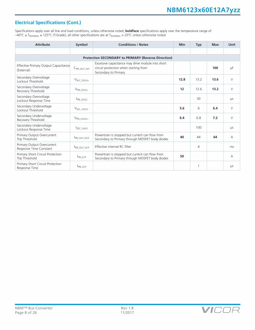
Protection SECONDARY to PRIMARY (Reverse Direction)
Effective Primary Output Capacitance (External)
CPRI_OUT_EXT
Excessive capacitance may drive module into short circuit protection when starting from Secondary to Primary
100 µF
Secondary Overvoltage Lockout Threshold
VSEC_OVLO+ 12.8 13.2 13.6 V
Secondary Overvoltage Recovery Threshold
VPRI_OVLO– 12 12.6 13.2 V
Secondary Overvoltage Lockout Response Time
tPRI_OVLO 30 µs
Secondary Undervoltage Lockout Threshold
VSEC_UVLO– 5.6 6 6.4 V
Secondary Undervoltage Recovery Threshold
VPRI_UVLO+– 6.4 6.8 7.2 V
Secondary Undervoltage Lockout Response Time
tSEC_UVLO 100 µs
Primary Output Overcurrent Trip Threshold
IPRI_OUT_OCPPowertrain is stopped but current can flow from Secondary to Primary through MOSFET body diodes
40 44 64 A
Primary Output Overcurrent Response Time Constant
tPRI_OUT_OCP Effective internal RC filter 4 ms
Primary Short Circuit Protection Trip Threshold
IPRI_SCPPowertrain is stopped but current can flow from Secondary to Primary through MOSFET body diodes
50 A
Primary Short Circuit Protection Response Time
tPRI_SCP 1 µs
Electrical Specifications (Cont.)
Specifications apply over all line and load conditions, unless otherwise noted; boldface specifications apply over the temperature range of –40°C ≤ TINTERNAL ≤ 125°C (T-Grade); all other specifications are at TINTERNAL = 25ºC unless otherwise noted.
NBM™ Bus Converter Rev 1.8Page 9 of 26 11/2017
NBM6123x60E12A7yzz
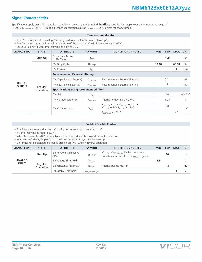
Seco
ndar
y O
utpu
t Cur
rent
(A)
Primary Input Voltage (V)
ISEC_OUT_DC ISEC_OUT_PULSE
0 20 40 60 80
100 120 140 160 180 200 220
36 38 40 42 44 46 48 50 52 54 56 58 60
Seco
ndar
y O
utpu
t Pow
er (W
)
Primary Input Voltage (V)
PSEC_OUT_DC PSEC_OUT_PULSE
0 250 500 750
1000 1250 1500 1750 2000 2250 2500
36 38 40 42 44 46 48 50 52 54 56 58 60
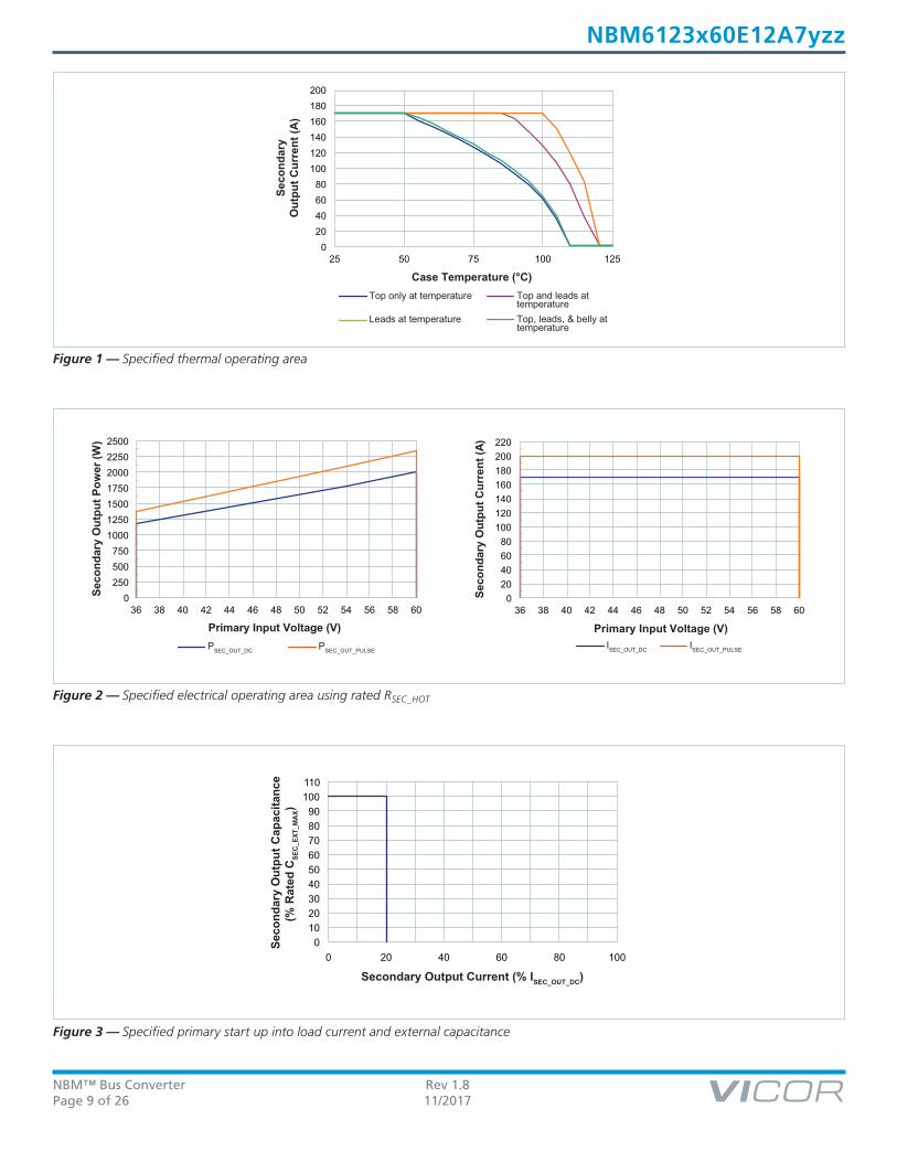
Figure 1 — Specified thermal operating area
Figure 2 — Specified electrical operating area using rated RSEC_HOT
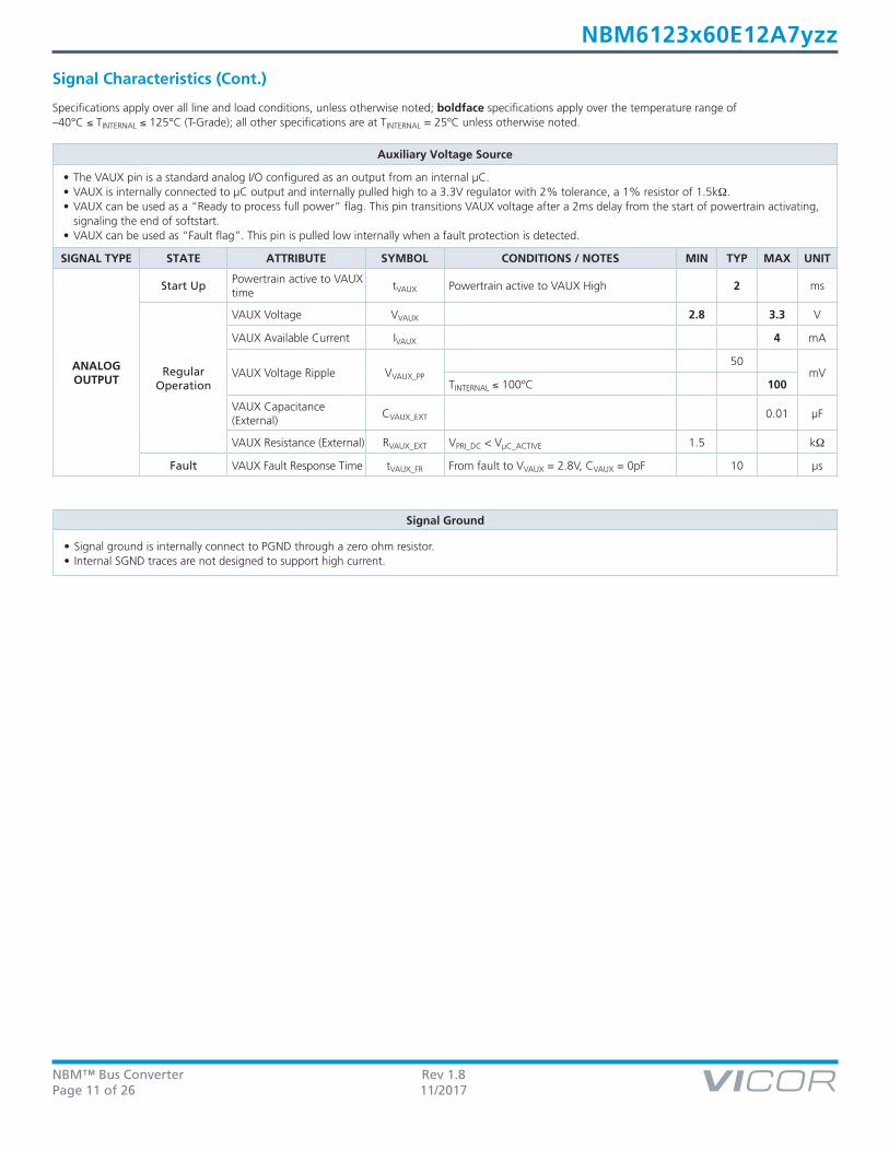
Seco
ndar
y O
utpu
t Cap
acita
nce
(% R
ated
CSE
C_E
XT_M
AX)
Secondary Output Current (% ISEC_OUT_DC)
0 10 20 30 40 50 60 70 80 90
100 110
0 20 40 60 80 100
Seco
ndar
yO
utpu
t Cur
rent
(A)
Case Temperature (°C) Top only at temperature
Leads at temperature
Top and leads attemperatureTop, leads, & belly attemperature
0 20 40 60 80
100 120 140 160 180 200
25 50 75 100 125
Figure 3 — Specified primary start up into load current and external capacitance
NBM™ Bus Converter Rev 1.8Page 10 of 26 11/2017
NBM6123x60E12A7yzz
Signal Characteristics
Specifications apply over all line and load conditions, unless otherwise noted; boldface specifications apply over the temperature range of –40°C ≤ TINTERNAL ≤ 125°C (T-Grade); all other specifications are at TINTERNAL = 25ºC unless otherwise noted.
Temperature Monitor
• The TM pin is a standard analog I/O configured as an output from an internal µC.• The TM pin monitors the internal temperature of the controller IC within an accuracy of ±5°C.• µC 250kHz PWM output internally pulled high to 3.3V.
SIGNAL TYPE STATE ATTRIBUTE SYMBOL CONDITIONS / NOTES MIN TYP MAX UNIT
DIGITALOUTPUT
Start UpPowertrain Active to TM Time
tTM 100 µs
RegularOperation
TM Duty Cycle TMPWM 18.18 68.18 %
TM Current ITM 4 mA
Recommended External filtering
TM Capacitance (External) CTM_EXT Recommended External filtering 0.01 µF
TM Resistance (External) RTM_EXT Recommended External filtering 1 kΩ
Specifications using recommended filter
TM Gain ATM 10 mV / °C
TM Voltage Reference VTM_AMB Internal temperature = 27ºC 1.27 V
TM Voltage Ripple VTM_PP
RTM_EXT = 1kΩ, CTM_EXT = 0.01µF, VPRI_DC = 54V, ISEC_DC = 170A
28mV
TINTERNAL ≤ 100ºC 40
Enable / Disable Control
• The EN pin is a standard analog I/O configured as an input to an internal µC.• It is internally pulled high to 3.3V.• When held low, the NBM internal bias will be disabled and the powertrain will be inactive.• In an array of NBMs, EN pins should be interconnected to synchronize start up.• Unit must not be disabled if a load is present on +VPRI while in reverse operation.
SIGNAL TYPE STATE ATTRIBUTE SYMBOL CONDITIONS / NOTES MIN TYP MAX UNIT
ANALOGINPUT
Start UpEN to Powertrain active time
tEN_STARTVPRI_DC > VPRI_UVLO+, EN held low both conditions satisfied for T > tPRI_UVLO+_DELAY
10 ms
Regular Operation
EN Voltage Threshold VEN_TH 2.3 V
EN Resistance (Internal) REN_INT Internal pull up resistor 1.5 kΩ
EN Disable Threshold VEN_DISABLE_TH 1 V
NBM™ Bus Converter Rev 1.8Page 11 of 26 11/2017
NBM6123x60E12A7yzz
Auxiliary Voltage Source
• The VAUX pin is a standard analog I/O configured as an output from an internal µC.• VAUX is internally connected to µC output and internally pulled high to a 3.3V regulator with 2% tolerance, a 1% resistor of 1.5kΩ.• VAUX can be used as a “Ready to process full power” flag. This pin transitions VAUX voltage after a 2ms delay from the start of powertrain activating,
signaling the end of softstart.• VAUX can be used as “Fault flag”. This pin is pulled low internally when a fault protection is detected.
SIGNAL TYPE STATE ATTRIBUTE SYMBOL CONDITIONS / NOTES MIN TYP MAX UNIT
ANALOGOUTPUT
Start UpPowertrain active to VAUX time
tVAUX Powertrain active to VAUX High 2 ms
RegularOperation
VAUX Voltage VVAUX 2.8 3.3 V
VAUX Available Current IVAUX 4 mA
VAUX Voltage Ripple VVAUX_PP
50mV
TINTERNAL ≤ 100ºC 100
VAUX Capacitance (External)
CVAUX_EXT 0.01 µF
VAUX Resistance (External) RVAUX_EXT VPRI_DC < VµC_ACTIVE 1.5 kΩ
Fault VAUX Fault Response Time tVAUX_FR From fault to VVAUX = 2.8V, CVAUX = 0pF 10 µs
Signal Characteristics (Cont.)
Specifications apply over all line and load conditions, unless otherwise noted; boldface specifications apply over the temperature range of –40°C ≤ TINTERNAL ≤ 125°C (T-Grade); all other specifications are at TINTERNAL = 25ºC unless otherwise noted.
Signal Ground
• Signal ground is internally connect to PGND through a zero ohm resistor.• Internal SGND traces are not designed to support high current.

NBM™ Bus Converter Rev 1.8Page 12 of 26 11/2017
NBM6123x60E12A7yzz
NBM Forward Direction Timing Diagram
EN TM+VPR
I
BIDI
R
INPU
T
+VSE
C
OU
TPU
T
VPRI_DCINPUT TURN-O
N SECONDARY OUTPUT
TURN-ON PRIM
ARY INPUT OVERVOLT
AGE
VPRI_DCINPUT REST
ART
ENABLE PULLE
D LOW
ENABLE PULLE
D HIGH SHORT CIRCUIT EVENT PRIM
ARY INPUT VOLT
AGE
TURN-OFF
OU
TPU
T
OU
TPU
T
V AU
X
EN & VAUX IN
TERNAL Pull-u
p
OVE
RVO
LTAG
EST
ARTU
PEN
ABLE
CO
NTR
OL O
VERC
URR
ENT
SHU
TDO
WN
µcINITIALIZ
E
VP
RI_
OV
LO-
VP
RI_
OV
LO+
VPR
I_U
VLO
+V
µC_A
CTI
VE
VN
OM
V PR
I_U
VLO
-
t SE
C_O
UT_
SC
Pt P
RI_
UVL
O+_
DEL
AY
t VA
UX
t AU
TO-R
ESTA
RT
> t P
RI_
UVL
O+_
DEL
AY
NBM™ Bus Converter Rev 1.8Page 13 of 26 11/2017
NBM6123x60E12A7yzz
NBM Reverse Direction Timing Diagram
EN TM+VSE
C
BIDI
R
INPU
T
+VPR
I
OU
TPU
T
VSEC_DCIN
PUT TURN-ON PRIM
ARY OUTPUT
TURN-ON SE
CONDARY OVERVOLTAGE
VSEC_DCINPUT REST
ART
ENABLE PULLE
D LOW
ENABLE PULLE
D HIGHOVER CURRENT /
SHORT CIRCUIT EVENT
SECONDARY IN
PUT
VOLTAGE TURN-O
FF
OU
TPU
T
OU
TPU
T
V AU
X
EN & VAUX IN
TERNAL Pull-u
pO
VERV
OLT
AGE
STAR
TUP
ENAB
LE C
ON
TRO
LO
VERC
URR
ENT
SHU
TDO
WN
µcINITIALIZE
VS
EC_O
VLO
-V S
EC
_OVL
O+
VS
EC
_UV
LO+
VµC
_AC
TIV
E
VN
OM
VS
EC_U
VLO
-
t PR
I_O
UT_
OC
Pt P
RI_
UV
LO+_
DE
LAY
t VA
UX
t AU
TO-R
ES
TAR
T
> t P
RI_
UV
LO+_
DE
LAY
V PR
I =+V
SEC
–(~
1.4V
)
NO
T SU
PPO
RTED
CO
NDI
TIO
N,
PERM
ANEN
T DA
MAG
E M
AY O
CCU
R
RED
LIN
E: L
OAD
MU
ST N
OT
BE P
RESE
NT
TO P
REVE
NT
DAM
AGE
TO U
NIT

NBM™ Bus Converter Rev 1.8Page 14 of 26 11/2017
NBM6123x60E12A7yzz
FAULT
SEQUENCE
TM Low
EN High
VAUX Low
Powertrain Stopped
VµC_ACTIVE < VPRI_DC < VPRI_UVLO+
VPRI_DC > VPRI_UVLO+
or VSEC_DC > VSEC_UVLO+
tPRI_UVLO+_DELAY
expiredONE TIME DELAYINITIAL STARTUPFault
Auto-recovery
ENABLE falling edge,or OTP detected
Input OVLO or UVLO,Output OCP,
UTP, OVLO or UVLO, or Input OCP detected
ENABLE falling edge,or OTP detected
Input OVLO or UVLO,Output OCP,
UTP, OVLO or UVLO, or Input OCP detected
Short Circuit detected
SUSTAINED
OPERATION
TM PWM
EN High
VAUX High
Powertrain Active
STARTUP SEQUENCE
TM Low
EN High
VAUX Low
Powertrain Stopped
STANDBY SEQUENCE
TM Low
EN High
VAUX Low
Powertrain Stopped
Note: During reverse direction operation a load must not be present if the powertrain is in any stopped state while the supply voltage is present on +VSEC.
VµC_ACTIVE < VSEC_DC
< VPRI_UVLO+ K
Applicationof input voltage to VPRI_DC
Applicationof input voltage to VSEC_DC
High Level Functional State Diagram
Conditions that cause state transitions are shown along arrows. Sub-sequence activities listed inside the state bubbles.
NBM™ Bus Converter Rev 1.8Page 15 of 26 11/2017
NBM6123x60E12A7yzz
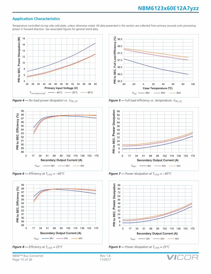
Application Characteristics
Temperature controlled via top side cold plate, unless otherwise noted. All data presented in this section are collected from primary sourced units processing power in forward direction. See associated figures for general trend data.
PRI t
o SE
C, P
ower
Dis
sipa
tion
(W)
Primary Input Voltage (V) - 40°C 25°C 90°CTTOP SURFACE CASE:
4
6
8
10
12
14
16
18
36 38 40 42 44 46 48 50 52 54 56 58 60
Case Temperature (ºC) 36V 54V 60V
PRI t
o SE
C, F
ull L
oad
Effic
ienc
y (%
)
VPRI:
95.5
96.0
96.5
97.0
97.5
98.0
98.5
-40 -20 0 20 40 60 80 100
PRI t
o SE
C, E
ffici
ency
(%)
Secondary Output Current (A) 36V 54V 60VVPRI :
88 89 90 91 92 93 94 95 96 97 98 99
0 17 34 51 68 85 102 119 136 153 170
Figure 4 — No load power dissipation vs. VPRI_DC Figure 5 — Full load efficiency vs. temperature; VPRI_DC
Figure 6 — Efficiency at TCASE = –40°C
PRI t
o SE
C, P
ower
Dis
sipa
tion
Secondary Output Current (A) 36V 54V 60V
VPRI :
0 8
16 24 32 40 48 56 64 72 80 88
0 17 34 51 68 85 102 119 136 153 170
Figure 9 — Power dissipation at TCASE = 25°C
PRI t
o SE
C, E
ffici
ency
(%)
Secondary Output Current (A) 36V 54V 60V
VPRI :
88 89 90 91 92 93 94 95 96 97 98 99
0 17 34 51 68 85 102 119 136 153 170
Figure 8 — Efficiency at TCASE = 25°C
PRI t
o SE
C, P
ower
Dis
sipa
tion
Secondary Output Current (A) 36V 54V 60VVPRI :
0 17 34 51 68 85 102 119 136 153 170 0 8
16 24 32 40 48 56 64 72 80 88
Figure 7 — Power dissipation at TCASE = –40°C
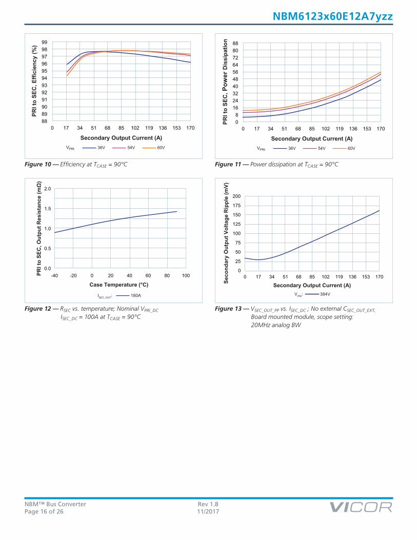
NBM™ Bus Converter Rev 1.8Page 16 of 26 11/2017
NBM6123x60E12A7yzz
Secondary Output Current (A) 384VVPRI:
Seco
ndar
y O
utpu
t Vol
tage
Rip
ple
(mV)
0
25
50
75
100
125
150
175
200
0 17 34 51 68 85 102 119 136 153 170
Figure 13 — VSEC_OUT_PP vs. ISEC_DC ; No external CSEC_OUT_EXT. Board mounted module, scope setting: 20MHz analog BW
Secondary Output Current (A) 36V 54V 60VVPRI:
PRI t
o SE
C, E
ffici
ency
(%)
88 89 90 91 92 93 94 95 96 97 98 99
0 17 34 51 68 85 102 119 136 153 170
Figure 10 — Efficiency at TCASE = 90°C
Case Temperature (°C)
180AISEC_OUT:
PRI t
o SE
C, O
utpu
t Res
ista
nce
(mΩ
)
0.0
0.5
1.0
1.5
2.0
-40 -20 0 20 40 60 80 100
Figure 12 — RSEC vs. temperature; Nominal VPRI_DC ISEC_DC = 100A at TCASE = 90°C
Secondary Output Current (A) 36V 54V 60VVPRI:
PRI t
o SE
C, P
ower
Dis
sipa
tion
0 8
16 24 32 40 48 56 64 72 80 88
0 17 34 51 68 85 102 119 136 153 170
Figure 11 — Power dissipation at TCASE = 90°C
NBM™ Bus Converter Rev 1.8Page 17 of 26 11/2017
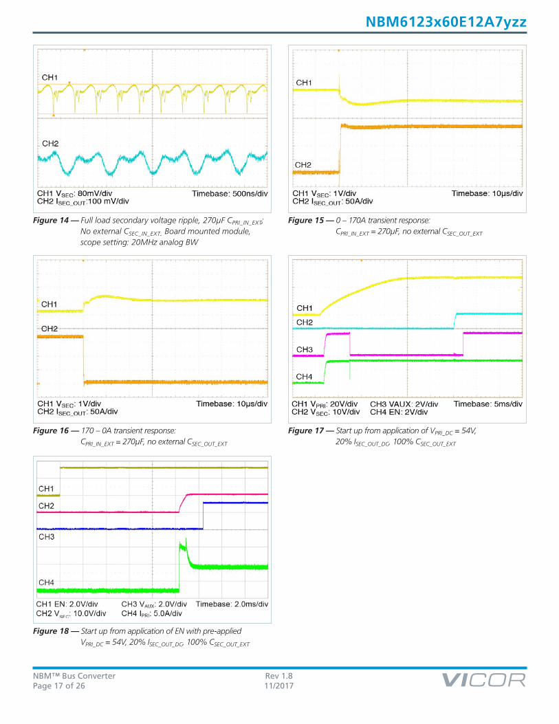
NBM6123x60E12A7yzz
Figure 15 — 0 – 170A transient response: CPRI_IN_EXT = 270µF, no external CSEC_OUT_EXT
Figure 14 — Full load secondary voltage ripple, 270µF CPRI_IN_EXT; No external CSEC_IN_EXT. Board mounted module, scope setting: 20MHz analog BW
Figure 16 — 170 – 0A transient response: CPRI_IN_EXT = 270µF, no external CSEC_OUT_EXT
Figure 17 — Start up from application of VPRI_DC = 54V, 20% ISEC_OUT_DC, 100% CSEC_OUT_EXT
Figure 18 — Start up from application of EN with pre-applied VPRI_DC = 54V, 20% ISEC_OUT_DC, 100% CSEC_OUT_EXT
NBM™ Bus Converter Rev 1.8Page 18 of 26 11/2017
NBM6123x60E12A7yzz
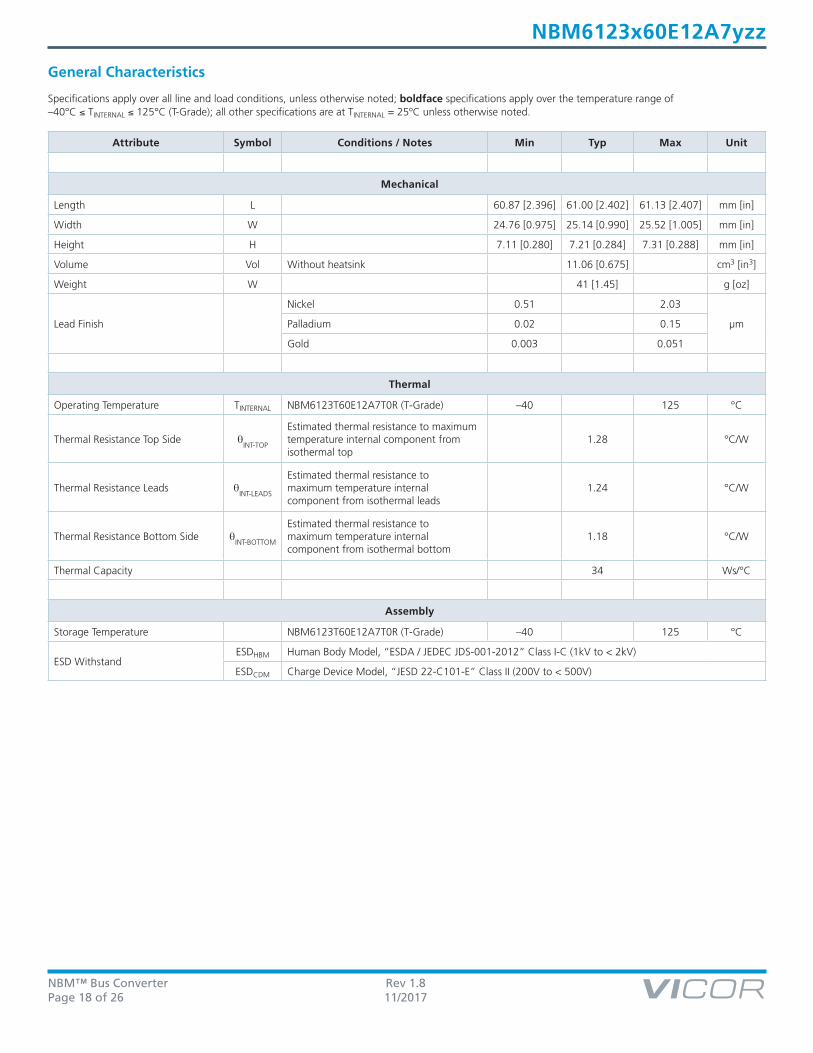
General Characteristics
Specifications apply over all line and load conditions, unless otherwise noted; boldface specifications apply over the temperature range of –40°C ≤ TINTERNAL ≤ 125°C (T-Grade); all other specifications are at TINTERNAL = 25ºC unless otherwise noted.
Attribute Symbol Conditions / Notes Min Typ Max Unit
Mechanical
Length L 60.87 [2.396] 61.00 [2.402] 61.13 [2.407] mm [in]
Width W 24.76 [0.975] 25.14 [0.990] 25.52 [1.005] mm [in]
Height H 7.11 [0.280] 7.21 [0.284] 7.31 [0.288] mm [in]
Volume Vol Without heatsink 11.06 [0.675] cm3 [in3]
Weight W 41 [1.45] g [oz]
Lead Finish
Nickel 0.51 2.03
µmPalladium 0.02 0.15
Gold 0.003 0.051
Thermal
Operating Temperature TINTERNAL NBM6123T60E12A7T0R (T-Grade) –40 125 °C
Thermal Resistance Top Side θINT-TOP
Estimated thermal resistance to maximum temperature internal component from isothermal top
1.28 °C/W
Thermal Resistance Leads θINT-LEADS
Estimated thermal resistance to maximum temperature internal component from isothermal leads
1.24 °C/W
Thermal Resistance Bottom Side θINT-BOTTOM
Estimated thermal resistance to maximum temperature internal component from isothermal bottom
1.18 °C/W
Thermal Capacity 34 Ws/°C
Assembly
Storage Temperature NBM6123T60E12A7T0R (T-Grade) –40 125 °C
ESD WithstandESDHBM Human Body Model, “ESDA / JEDEC JDS-001-2012” Class I-C (1kV to < 2kV)
ESDCDM Charge Device Model, “JESD 22-C101-E” Class II (200V to < 500V)

NBM™ Bus Converter Rev 1.8Page 19 of 26 11/2017
NBM6123x60E12A7yzz
[b] Product is not intended for reflow solder attach.
General Characteristics (Cont.)
Specifications apply over all line and load conditions, unless otherwise noted; boldface specifications apply over the temperature range of –40°C ≤ TINTERNAL ≤ 125°C (T-Grade); all other specifications are at TINTERNAL = 25ºC unless otherwise noted.
Attribute Symbol Conditions / Notes Min Typ Max Unit
Soldering [b]
Peak Temperature Top Case 135 °C
Safety
Isolation voltage / Dielectric Test VHIPOT
PRIMARY to SECONDARY N/A
VPRIMARY to CASE 2250
SECONDARY to CASE 2250
Isolation Capacitance CPRI_SEC Unpowered Unit N/A N/A N/A pF
Insulation Resistance RPRI_SEC At 500VDC 0 MΩ
MTBF
MIL-HDBK-217Plus Parts Count - 25°C Ground Benign, Stationary, Indoors / Computer
3.34 MHrs
Telcordia Issue 2 - Method I Case III; 25°C Ground Benign, Controlled
5.26 MHrs
Agency Approvals / Standards
cTÜVus EN 60950-1
cURus UL 60950-1
CE Marked for Low Voltage Directive and RoHS Recast Directive, as applicable
NBM™ Bus Converter Rev 1.8Page 20 of 26 11/2017
NBM6123x60E12A7yzz
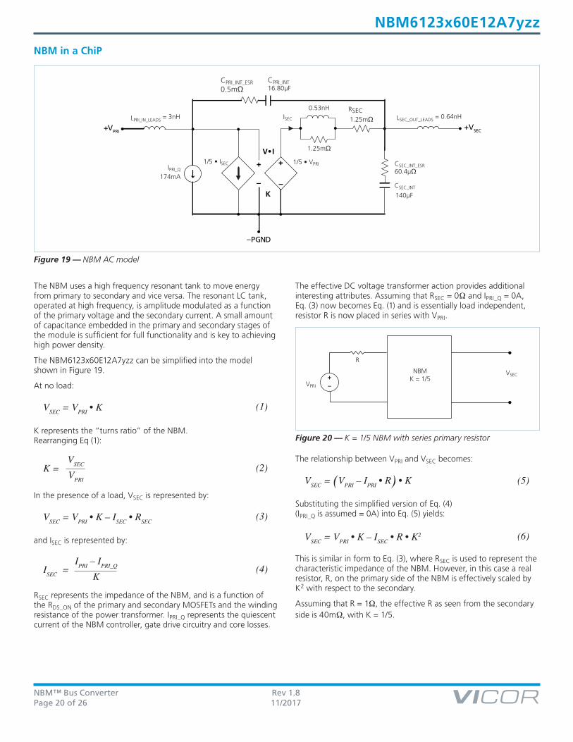
The NBM uses a high frequency resonant tank to move energy from primary to secondary and vice versa. The resonant LC tank, operated at high frequency, is amplitude modulated as a function of the primary voltage and the secondary current. A small amount of capacitance embedded in the primary and secondary stages of the module is sufficient for full functionality and is key to achieving high power density.
The NBM6123x60E12A7yzz can be simplified into the model shown in Figure 19.
At no load:
K represents the “turns ratio” of the NBM. Rearranging Eq (1):
In the presence of a load, VSEC is represented by:
and ISEC is represented by:
RSEC represents the impedance of the NBM, and is a function of the RDS_ON of the primary and secondary MOSFETs and the winding resistance of the power transformer. IPRI_Q represents the quiescent current of the NBM controller, gate drive circuitry and core losses.
The effective DC voltage transformer action provides additional interesting attributes. Assuming that RSEC = 0Ω and IPRI_Q = 0A, Eq. (3) now becomes Eq. (1) and is essentially load independent, resistor R is now placed in series with VPRI.
The relationship between VPRI and VSEC becomes:
Substituting the simplified version of Eq. (4) (IPRI_Q is assumed = 0A) into Eq. (5) yields:
This is similar in form to Eq. (3), where RSEC is used to represent the characteristic impedance of the NBM. However, in this case a real resistor, R, on the primary side of the NBM is effectively scaled by K2 with respect to the secondary.
Assuming that R = 1Ω, the effective R as seen from the secondary side is 40mΩ, with K = 1/5.
+VSEC+VPRI
V•I
K
+
–
+
–
–PGND
174mA
1/5 • ISEC 1/5 • VPRI
CPRI_INT_ESR
0.5mΩ
0.53nH
140µF
IPRI_Q
lPRI_IN_LEADS = 3nH ISEC
R
SACK = 1/32Vin
Vout+–VPRI
VSEC
R
NBMK = 1/5
Figure 20 — K = 1/5 NBM with series primary resistor
Figure 19 — NBM AC model
CSEC_INT
lSEC_OUT_LEADS = 0.64nH
CPRI_INT16.80µF
1.25mΩRSEC
CSEC_INT_ESR
60.4µΩ
NBM in a ChiP
1.25mΩ
VSEC = VPRI • K (1)
K = (2)VSEC
VPRI
ISEC = (4)IPRI – IPRI_Q
K
VSEC = VPRI • K – ISEC • RSEC (3)
VSEC = (VPRI – IPRI • R) • K (5)
VSEC = VPRI • K – ISEC • R • K2 (6)
NBM™ Bus Converter Rev 1.8Page 21 of 26 11/2017
NBM6123x60E12A7yzz
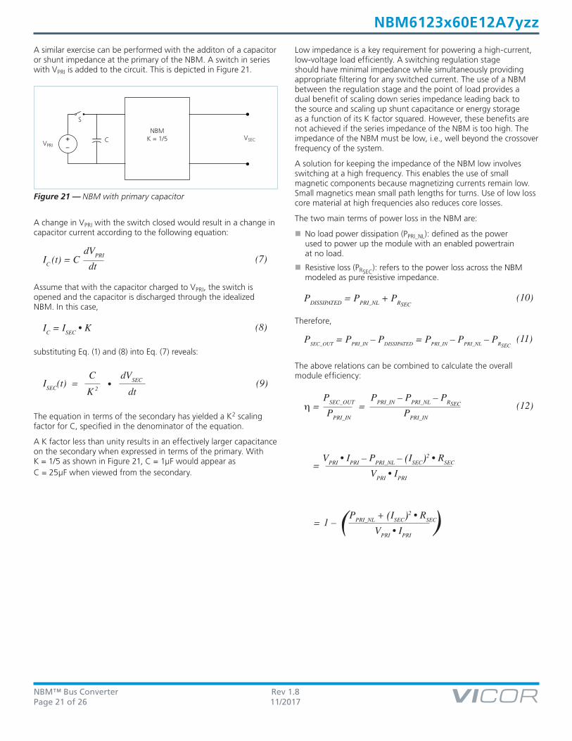
A similar exercise can be performed with the additon of a capacitor or shunt impedance at the primary of the NBM. A switch in series with VPRI is added to the circuit. This is depicted in Figure 21.
A change in VPRI with the switch closed would result in a change in capacitor current according to the following equation:
Assume that with the capacitor charged to VPRI, the switch is opened and the capacitor is discharged through the idealized NBM. In this case,
substituting Eq. (1) and (8) into Eq. (7) reveals:
The equation in terms of the secondary has yielded a K2 scaling factor for C, specified in the denominator of the equation.
A K factor less than unity results in an effectively larger capacitance on the secondary when expressed in terms of the primary. With K = 1/5 as shown in Figure 21, C = 1µF would appear as C = 25µF when viewed from the secondary.
Low impedance is a key requirement for powering a high-current, low-voltage load efficiently. A switching regulation stage should have minimal impedance while simultaneously providing appropriate filtering for any switched current. The use of a NBM between the regulation stage and the point of load provides a dual benefit of scaling down series impedance leading back to the source and scaling up shunt capacitance or energy storage as a function of its K factor squared. However, these benefits are not achieved if the series impedance of the NBM is too high. The impedance of the NBM must be low, i.e., well beyond the crossover frequency of the system.
A solution for keeping the impedance of the NBM low involves switching at a high frequency. This enables the use of small magnetic components because magnetizing currents remain low. Small magnetics mean small path lengths for turns. Use of low loss core material at high frequencies also reduces core losses.
The two main terms of power loss in the NBM are:
■n No load power dissipation (PPRI_NL): defined as the power used to power up the module with an enabled powertrain at no load.
■n Resistive loss (PRSEC): refers to the power loss across the NBM
modeled as pure resistive impedance.
Therefore,
The above relations can be combined to calculate the overall module efficiency:
C
S
SACK = 1/32Vin
Vout+–
VPRI
VSECCNBM
K = 1/5
Figure 21 — NBM with primary capacitor
S
IC (t) = C (7) dVPRI
dt
ISEC(t) = CK 2
dVSEC
dt• (9)
IC = ISEC • K (8)
PDISSIPATED = PPRI_NL + PRSEC(10)
PSEC_OUT = PPRI_IN – PDISSIPATED = PPRI_IN – PPRI_NL – PRSEC(11)
η = (12)PSEC_OUT
PPRI_IN
PPRI_IN – PPRI_NL – PRSEC
PPRI_IN=
VPRI • IPRI – PPRI_NL – (ISEC)2 • RSEC
VPRI • IPRI
=
PPRI_NL + (ISEC)2 • RSEC
VPRI • IPRI
= 1 – ( )
NBM™ Bus Converter Rev 1.8Page 22 of 26 11/2017
NBM6123x60E12A7yzz
Input and Output Filter Design
A major advantage of NBM systems versus conventional PWM converters is that the auto-transformer based NBM does not require external filtering to function properly. The resonant LC tank, operated at extreme high frequency, is amplitude modulated as a function of primary voltage and secondary current and efficiently transfers charge through the auto-transformer. A small amount of capacitance embedded in the primary and secondary stages of the module is sufficient for full functionality and is key to achieving power density.
This paradigm shift requires system design to carefully evaluate external filters in order to:
■n Guarantee low source impedance:
To take full advantage of the NBM’s dynamic response, the impedance presented to its primary terminals must be low from DC to approximately 5MHz. The connection of the bus converter module to its power source should be implemented with minimal distribution inductance. If the interconnect inductance exceeds 100nH, the primary should be bypassed with a RC damper to retain low source impedance and stable operation. With an interconnect inductance of 200nH, the RC damper may be as high as 1µF in series with 0.3Ω. A single electrolytic or equivalent low-Q capacitor may be used in place of the series RC bypass.
■n Further reduce primary and/or secondary voltage ripple without sacrificing dynamic response:
Given the wide bandwidth of the module, the source response is generally the limiting factor in the overall system response. Anomalies in the response of the primary source will appear at the secondary of the module multiplied by its K factor.
■n Protect the module from overvoltage transients imposed by the system that would exceed maximum ratings and induce stresses:
The module primary/secondary voltage ranges shall not be exceeded. An internal overvoltage lockout function prevents operation outside of the normal operating primary range. Even when disabled, the powertrain is exposed to the applied voltage and the power MOSFETs must withstand it.
Total load capacitance of the NBM module shall not exceed the specified maximum. Owing to the wide bandwidth and low secondary impedance of the module, low-frequency bypass capacitance and significant energy storage may be more densely and efficiently provided by adding capacitance at the primary of the module. At frequencies <500kHz the module appears as an impedance of RSEC between the source and load.
Within this frequency range, capacitance at the primary appears as effective capacitance on the secondary per the relationship defined in Eq. (13).
This enables a reduction in the size and number of capacitors used in a typical system.
Thermal Considerations
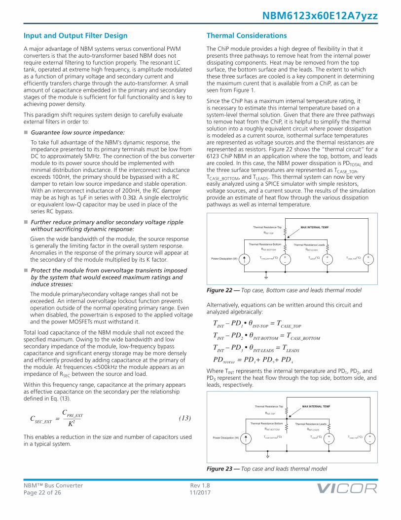
The ChiP module provides a high degree of flexibility in that it presents three pathways to remove heat from the internal power dissipating components. Heat may be removed from the top surface, the bottom surface and the leads. The extent to which these three surfaces are cooled is a key component in determining the maximum curent that is available from a ChiP, as can be seen from Figure 1.
Since the ChiP has a maximum internal temperature rating, it is necessary to estimate this internal temperature based on a system-level thermal solution. Given that there are three pathways to remove heat from the ChiP, it is helpful to simplify the thermal solution into a roughly equivalent circuit where power dissipation is modeled as a current source, isothermal surface temperatures are represented as voltage sources and the thermal resistances are represented as resistors. Figure 22 shows the “thermal circuit” for a 6123 ChiP NBM in an application where the top, bottom, and leads are cooled. In this case, the NBM power dissipation is PDTOTAL and the three surface temperatures are represented as TCASE_TOP, TCASE_BOTTOM, and TLEADS. This thermal system can now be very easily analyzed using a SPICE simulator with simple resistors, voltage sources, and a current source. The results of the simulation provide an estimate of heat flow through the various dissipation pathways as well as internal temperature.
Alternatively, equations can be written around this circuit and analyzed algebraically:
Where TINT represents the internal temperature and PD1, PD2, and PD3 represent the heat flow through the top side, bottom side, and leads, respectively.
+–
+–
+–
MAX INTERNAL TEMP
TCASE_BOTTOM
(°C) TLEADS
(°C) TCASE_TOP
(°C)Power Dissipation (W)
Thermal Resistance Top
Thermal Resistance Bottom Thermal Resistance Leads
+–
+–
MAX INTERNAL TEMP
TCASE_BOTTOM
(°C) TLEADS
(°C) TCASE_TOP
(°C)Power Dissipation (W)
Thermal Resistance Top
Thermal Resistance Bottom Thermal Resistance Leads
Figure 22 — Top case, Bottom case and leads thermal model
Figure 23 — Top case and leads thermal model
θINT-TOP
θINT-BOTTOM θINT-LEADS
θINT-TOP
θINT-BOTTOM θINT-LEADS
CSEC_EXT = (13) CPRI_EXT
K2
TINT – PD1 • θINT-TOP = TCASE_TOP
TINT – PD2 • θINT-BOTTOM = TCASE_BOTTOM
TINT – PD3 • θINT-LEADS = TLEADS
PDTOTAL = PD1+ PD2+ PD3
NBM™ Bus Converter Rev 1.8Page 23 of 26 11/2017
NBM6123x60E12A7yzz
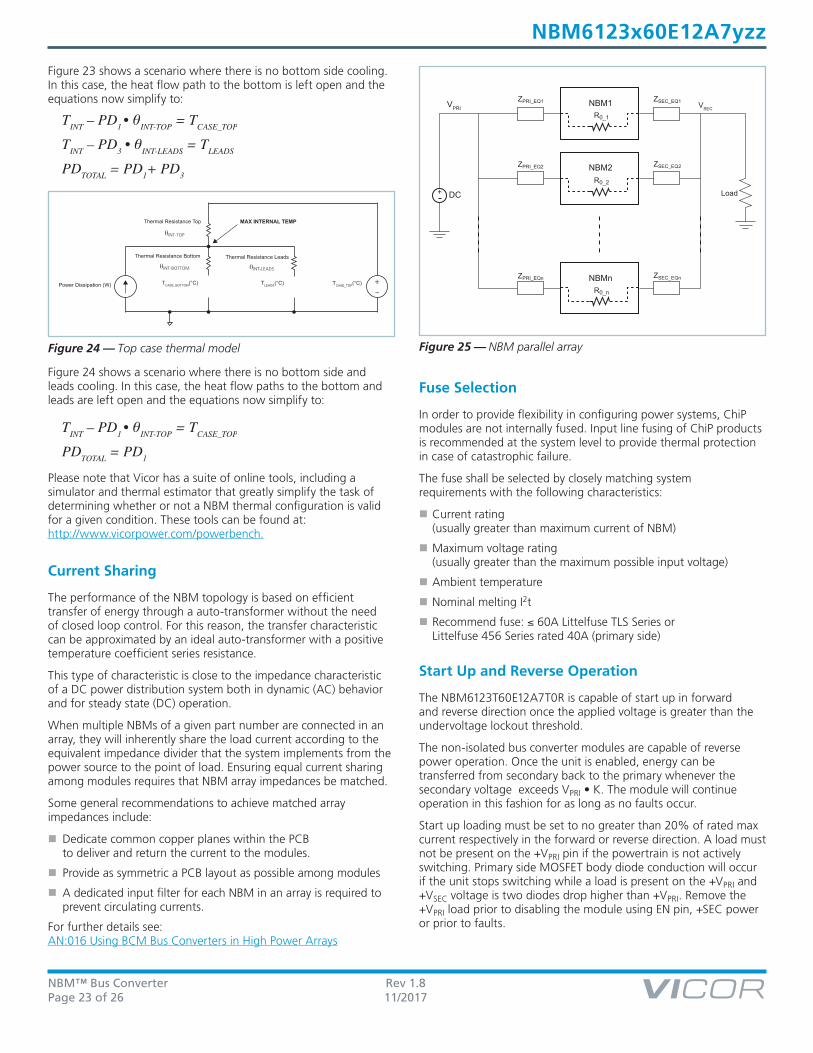
Figure 23 shows a scenario where there is no bottom side cooling. In this case, the heat flow path to the bottom is left open and the equations now simplify to:
Figure 24 shows a scenario where there is no bottom side and leads cooling. In this case, the heat flow paths to the bottom and leads are left open and the equations now simplify to:
Please note that Vicor has a suite of online tools, including a simulator and thermal estimator that greatly simplify the task of determining whether or not a NBM thermal configuration is valid for a given condition. These tools can be found at: http://www.vicorpower.com/powerbench.
Current Sharing
The performance of the NBM topology is based on efficient transfer of energy through a auto-transformer without the need of closed loop control. For this reason, the transfer characteristic can be approximated by an ideal auto-transformer with a positive temperature coefficient series resistance.
This type of characteristic is close to the impedance characteristic of a DC power distribution system both in dynamic (AC) behavior and for steady state (DC) operation.
When multiple NBMs of a given part number are connected in an array, they will inherently share the load current according to the equivalent impedance divider that the system implements from the power source to the point of load. Ensuring equal current sharing among modules requires that NBM array impedances be matched.
Some general recommendations to achieve matched array impedances include:
■n Dedicate common copper planes within the PCB to deliver and return the current to the modules.
■n Provide as symmetric a PCB layout as possible among modules
■n A dedicated input filter for each NBM in an array is required to prevent circulating currents.
For further details see: AN:016 Using BCM Bus Converters in High Power Arrays
Fuse Selection
In order to provide flexibility in configuring power systems, ChiP modules are not internally fused. Input line fusing of ChiP products is recommended at the system level to provide thermal protection in case of catastrophic failure.
The fuse shall be selected by closely matching system requirements with the following characteristics:
■n Current rating (usually greater than maximum current of NBM)
■n Maximum voltage rating (usually greater than the maximum possible input voltage)
■n Ambient temperature
■n Nominal melting I2t
■n Recommend fuse: ≤ 60A Littelfuse TLS Series or Littelfuse 456 Series rated 40A (primary side)
Start Up and Reverse Operation
The NBM6123T60E12A7T0R is capable of start up in forward and reverse direction once the applied voltage is greater than the undervoltage lockout threshold.
The non-isolated bus converter modules are capable of reverse power operation. Once the unit is enabled, energy can be transferred from secondary back to the primary whenever the secondary voltage exceeds VPRI • K. The module will continue operation in this fashion for as long as no faults occur.
Start up loading must be set to no greater than 20% of rated max current respectively in the forward or reverse direction. A load must not be present on the +VPRI pin if the powertrain is not actively switching. Primary side MOSFET body diode conduction will occur if the unit stops switching while a load is present on the +VPRI and +VSEC voltage is two diodes drop higher than +VPRI. Remove the +VPRI load prior to disabling the module using EN pin, +SEC power or prior to faults.
NBM1R0_1
ZPRI_EQ1 ZSEC_EQ1
ZSEC_EQ2
VSEC
ZSEC_EQn
ZPRI_EQ2
ZPRI_EQn
R0_2
R0_n
NBM2
NBMn
LoadDC
VPRI
+
Figure 25 — NBM parallel array
+–
MAX INTERNAL TEMP
TCASE_BOTTOM
(°C) TLEADS
(°C) TCASE_TOP
(°C)Power Dissipation (W)
Thermal Resistance Top
Thermal Resistance Bottom Thermal Resistance Leads
Figure 24 — Top case thermal model
θINT-TOP
θINT-BOTTOM θINT-LEADS
TINT – PD1 • θINT-TOP = TCASE_TOP
TINT – PD3 • θINT-LEADS = TLEADS
PDTOTAL = PD1+ PD3
TINT – PD1 • θINT-TOP = TCASE_TOP
PDTOTAL = PD1
NBM™ Bus Converter Rev 1.8Page 24 of 26 11/2017
NBM6123x60E12A7yzz
25.14±.38.990±.015
12.57.495
30.501.201
61.00±.132.402±.005
0
0 0
0
TOP VIEW (COMPONENT SIDE)
2.03.080
(9) PL.
1.02.040
(3) PL.
2.03.080
(9) PL.
1.02.040
(3) PL.
11.43.450
0
27.211.071(2) PL.
17.09.673
(2) PL.
7.94.312
(2) PL.
1.49.058
(2) PL.
18.05.710
(2) PL.
23.64.931
(2) PL.
21.94.864
(2) PL.
12.52.493
(2) PL.
3.37.132
(2) PL.
6.76.266
(2) PL.
20.84.820
(2) PL.
27.551.085(2) PL.
0 1
1.81
.465
11.
81.4
65
0
0
BOTTOM VIEW
.41.016
(24) PL.
7.21±.10.284±.004
4.17.164
(24) PL.
SEATINGPLANE
.05 [.002]
1.52±.08.060±.003
PLATED THRU.25 [.010]
ANNULAR RING(6) PL.
2.54±.08.100±.003
PLATED THRU.38 [.015]
ANNULAR RING(18) PL.
0
21.94±.08.864±.003
(2) PL.
12.52±.08.493±.003
(2) PL.
3.37±.08.132±.003
(2) PL.
6.76±.08.266±.003
(2) PL.
20.84±.08.820±.003
(2) PL.
27.55±.081.085±.003
(2) PL.
27.21±.081.071±.003
(2) PL.
17.09±.08.673±.003
(2) PL.
7.94±.08.312±.003
(2) PL.
1.49±.08.058±.003
(2) PL.
18.05±.08.710±.003
(2) PL.
23.64±.08.931±.003
(2) PL.
0
11
.81±
.08
.465
±.00
3
11
.81±
.08
.465
±.00
3
0
0
+VSEC +VSEC
+VSEC
+VSEC +VSEC
+VSEC
+VSEC +VSEC
PGND1 PGND2
PGND1 PGND2
PGND1 PGND2
PGND1 PGND2
+VPRI
+VPRI+VPRI
+VPRI
TM
ENVAUX
SGND
RECOMMENDED HOLE PATTERN(COMPONENT SIDE)
NOTES:
1- RoHS COMPLIANT PER CST-0001 LATEST REVISION.2- UNLESS OTHERWISE SPECIFIED DIMENSIONS ARE : INCH / [MM]
NBM Through Hole Package Mechanical Drawing and Recommended Land Pattern
NBM™ Bus Converter Rev 1.8Page 25 of 26 11/2017
NBM6123x60E12A7yzz
Revision History
Revision Date Description Page Number(s)
1.0 09/08/15 Initial Release n/a
1.1 09/28/15Changed PRI to SEC Input Quiescent CurrentAdded certifications
51 & 15
1.2 07/26/16Removed redundant informationUpdated information
new 19All
1.3 08/29/16Corrected the Secondary Output Overcurrent Response Time Constant Specification
6
1.4 09/12/2016 Corrected the enable to powertrain active time 10
1.5 05/26/17Efficiency and bidirectional start up and steady state summary points addedContent improvements
1All
1.6 07/28/17 Updated height specifications 1, 10, 24
1.7 09/21/17 Updated overcurrent protection specifications 6, 8
1.8 11/22/17 Updated TM voltage reference note 10

NBM™ Bus Converter Rev 1.8Page 26 of 26 11/2017
NBM6123x60E12A7yzz
Contact Us: http://www.vicorpower.com/contact-us
Vicor Corporation25 Frontage Road
Andover, MA, USA 01810Tel: 800-735-6200Fax: 978-475-6715
www.vicorpower.com
emailCustomer Service: [email protected]
Technical Support: [email protected]
Vicor’s comprehensive line of power solutions includes high density AC-DC and DC-DC modules and accessory components, fully configurable AC-DC and DC-DC power supplies, and complete custom power systems.
Information furnished by Vicor is believed to be accurate and reliable. However, no responsibility is assumed by Vicor for its use. Vicor makes no representations or warranties with respect to the accuracy or completeness of the contents of this publication. Vicor reserves the right to make changes to any products, specifications, and product descriptions at any time without notice. Information published by Vicor has been checked and is believed to be accurate at the time it was printed; however, Vicor assumes no responsibility for inaccuracies. Testing and other quality controls are used to the extent Vicor deems necessary to support Vicor’s product warranty. Except where mandated by government requirements, testing of all parameters of each product is not necessarily performed.
Specifications are subject to change without notice.
Visit http://www.vicorpower.com/NBM-Non-isolated-Bus-Converter-Module for the latest product information.
Vicor’s Standard Terms and Conditions and Product WarrantyAll sales are subject to Vicor’s Standard Terms and Conditions of Sale, and Product Warranty which are available on Vicor’s webpage (http://www.vicorpower.com/termsconditionswarranty) or upon request.
Life Support Policy
VICOR’S PRODUCTS ARE NOT AUTHORIZED FOR USE AS CRITICAL COMPONENTS IN LIFE SUPPORT DEVICES OR SYSTEMS WITHOUT THE EXPRESS PRIOR WRITTEN APPROVAL OF THE CHIEF EXECUTIVE OFFICER AND GENERAL COUNSEL OF VICOR CORPORATION. As used herein, life support devices or systems are devices which (a) are intended for surgical implant into the body, or (b) support or sustain life and whose failure to perform when properly used in accordance with instructions for use provided in the labeling can be reasonably expected to result in a significant injury to the user. A critical component is any component in a life support device or system whose failure to perform can be reasonably expected to cause the failure of the life support device or system or to affect its safety or effectiveness. Per Vicor Terms and Conditions of Sale, the user of Vicor products and components in life support applications assumes all risks of such use and indemnifies Vicor against all liability and damages.
Intellectual Property Notice
Vicor and its subsidiaries own Intellectual Property (including issued U.S. and Foreign Patents and pending patent applications) relating to the products described in this data sheet. No license, whether express, implied, or arising by estoppel or otherwise, to any intellectual property rights is granted by this document. Interested parties should contact Vicor’s Intellectual Property Department.
The products described on this data sheet are protected by the following U.S. Patents Numbers: 6,911,848; 6,930,893; 6,934,166; 7,145,786; 7,782,639; 8,427,269 and for use under 6,975,098 and 6,984,965.
©2017 Vicor Corporation. All rights reserved. The Vicor name is a registered trademark of Vicor Corporation.All other trademarks, product names, logos and brands are property of their respective owners.
Related Documents