Noise Analysis and Measurement for Current Mode and Voltage Mode Active Pixel Sensor Readout Methods by Dali Wu A thesis presented to the University of Waterloo in fulfillment of the thesis requirement for the degree of Master of Applied Science in Electrical and Computer Engineering Waterloo, Ontario, Canada, 2010 ©Dali Wu 2010

Welcome message from author
This document is posted to help you gain knowledge. Please leave a comment to let me know what you think about it! Share it to your friends and learn new things together.
Transcript
Noise Analysis and Measurement for
Current Mode and Voltage Mode Active
Pixel Sensor Readout Methods
by
Dali Wu
A thesis
presented to the University of Waterloo
in fulfillment of the
thesis requirement for the degree of
Master of Applied Science
in
Electrical and Computer Engineering
Waterloo, Ontario, Canada, 2010
©Dali Wu 2010

ii
AUTHOR'S DECLARATION
I hereby declare that I am the sole author of this thesis. This is a true copy of the thesis, including any
required final revisions, as accepted by my examiners.
I understand that my thesis may be made electronically available to the public.

iii
Abstract
A detailed experimental and theoretical investigation of noise in both current mode and
voltage mode amorphous silicon (a-Si) active pixel sensors (APS) has been performed in this
study. Both flicker (1/f) and thermal noise are considered. The experimental result in this
study emphasizes the computation of the output noise variance, and not the output noise
spectrum. This study determines which mode of operation is superior in term of output noise.
The current noise power spectral density of a single a-Si TFT is also measured in order to
find the suitable model for calculating the flicker noise. This experimental result matches
Hooge’s model. The theoretical analysis shows that the voltage mode APS has an advantage
over the current mode APS in terms of the flicker noise due to the operation of the readout
process. The experimental data are compared to the theoretical analysis and are in good
agreement. The results obtained in this study apply equally well to APS circuits made using
polycrystalline silicon (poly-Si) and single crystal silicon.

iv
Acknowledgements
I would like to express profound gratitude to my supervisor, Professor Karim S. Karim for
his invaluable support, encouragement, and supervision throughout my graduate study at the
University of Waterloo. His moral support and continuous technical guidance enabled me to
complete my work successfully. Also, I acknowledge my family for their unconditional
support throughout my study period.
Much of the work in this thesis could not have been completed without the help, discussion,
and cooperation from the following individuals: Dr. Nader Safavian who proposed this thesis
project for me, Mohammad Yazdandoost for his help with the experimental setup, Hadi Izadi
who essentially helped me with very aspect of my thesis work, and Amir Golden for his
insightful suggestion on measuring methods.

v
Table of Contents AUTHOR'S DECLARATION ............................................................................................................... ii
Abstract ................................................................................................................................................. iii
Acknowledgements ............................................................................................................................... iv
Table of Contents ................................................................................................................................... v
List of Figures ...................................................................................................................................... vii
List of Tables ......................................................................................................................................... ix
Chapter 1 Introduction ............................................................................................................................ 1
1.1 Purpose of the Research ............................................................................................................... 1
1.2 Solid State Electronic Imagers ..................................................................................................... 1
1.3 Flat Panel Imagers for Large Area Imaging ................................................................................. 2
1.4 X-ray and X-ray Detection Schemes ............................................................................................ 4
1.4.1 Introduction to X-ray ............................................................................................................. 4
1.4.2 Indirect and Direct X-ray Detection ...................................................................................... 5
1.5 Material Properties of Amorphous Silicon ................................................................................... 6
1.5.1 Metastability .......................................................................................................................... 9
1.5.2 Amorphous Thin Film Transistor Structure ........................................................................ 12
Chapter 2 Pixel Architectures for Large Area Digital Imaging ............................................................ 13
2.1 Passive Pixel Sensor Architecture .............................................................................................. 13
2.1.1 Introduction ......................................................................................................................... 13
2.1.2 Operation ............................................................................................................................. 14
2.1.3 Readout and Reset Speed .................................................................................................... 15
2.1.4 Voltage Sensing PPS ........................................................................................................... 17
2.2 Active Pixel Sensor .................................................................................................................... 18
2.2.1 Introduction ......................................................................................................................... 18
2.2.2 Current Mode APS .............................................................................................................. 19
2.2.3 Voltage Mode APS .............................................................................................................. 24
2.3 Two-Transistor Pixel Architecture ............................................................................................. 25
2.3.1 Gate Switching 2T APS ....................................................................................................... 25
2.3.2 Source Switching 2T APS ................................................................................................... 27
2.3.3 Drain Switching 2T APS ..................................................................................................... 29
2.4 Hybrid Pixel Design ................................................................................................................... 30
vi
2.4.1 Linearity and Gain .............................................................................................................. 31
Chapter 3 Noise Analysis of Current Mode and Voltage Mode APS .................................................. 32
3.1 Introduction ................................................................................................................................ 32
3.2 Introduction to Electrical Noise ................................................................................................. 32
3.2.1 Thermal Noise ..................................................................................................................... 32
3.2.2 Flicker Noise ....................................................................................................................... 33
3.3 Noise in Current Mode APS ...................................................................................................... 35
3.4 Noise in Voltage Mode APS ...................................................................................................... 44
Chapter 4 Noise Measurement ............................................................................................................. 47
4.1 Noise Measurement of a Single TFT ......................................................................................... 47
4.1.1 Measurement Setup ............................................................................................................. 47
4.1.2 Flicker Noise ....................................................................................................................... 48
4.2 Noise Measurement for C-APS and V-APS .............................................................................. 51
4.2.1 Test Structure and Measurement Setup............................................................................... 51
4.2.2 Measurement Results for C-APS ........................................................................................ 56
4.2.3 Measurement Results for V-APS ........................................................................................ 60
Chapter 5 Conclusion ........................................................................................................................... 65
5.1 Summary .................................................................................................................................... 65
5.2 Projected Results ........................................................................................................................ 65
5.3 Potential Future Research .......................................................................................................... 68
References ............................................................................................................................................ 69
vii
List of Figures Figure 1: X-ray imaging with large area imager ............................................................................ 2
Figure 2: AMFPI Imaging System diagram ................................................................................... 3
Figure 3: Indirect X-ray detection mechanism ............................................................................... 5
Figure 4: Direct X-ray detection scheme ........................................................................................ 6
Figure 5: Diagram of amorphous silicon network with hydrogen atom passivation ...................... 7
Figure 6: Energy distribution versus density of state ..................................................................... 8
Figure 7: Structure of a top gate a-Si TFT .................................................................................... 12
Figure 8: Passive pixel sensor architecture ................................................................................... 13
Figure 9: PPS structure connecting to a column charge amplifier ............................................... 15
Figure 10: Small signal model for a PPS structure connecting to a column charge amplifier ..... 16
Figure 11: PPS structure connecting to a column voltage amplifier ............................................ 18
Figure 12: (a): circuit diagram of 3-T APS in current mode. (b): circuit diagram of 3-T APS in
voltage mode ........................................................................................................................ 19
Figure 13: Circuit diagram used to derive the output current for the C-APS ............................... 21
Figure 14: C-APS with column current sink ................................................................................ 24
Figure 15: Gate switching 2T APS ............................................................................................... 26
Figure 16: Operation modes for 2T gate switching APS .............................................................. 27
Figure 17: Source switching 2T APS ........................................................................................... 27
Figure 18: Operation modes for 2T source switching APS .......................................................... 28
Figure 19: Source switching 2T APS ........................................................................................... 30
Figure 20: Operation modes for 2T drain switching APS ............................................................ 30
Figure 21: 4T hybrid pixel sensor ................................................................................................ 31
Figure 22: Small signal model of C-APS during readout ............................................................. 36
Figure 23: Noise model for the charge amplifier ......................................................................... 41
Figure 24: Small signal model of V-APS during (a) Phase 1 of the readout, and (b) Phase 2 of
the readout. ........................................................................................................................... 45
Figure 25: Noise experiment setup for a single TFT .................................................................... 48
Figure 26: Noise current power spectral density for an a-Si TFT in the linear mode. (a): Noise
spectra ranges from 10 Hz to 1 MHz. (b): Noise spectra in low frequency range (10 Hz to
100 Hz). ................................................................................................................................ 49
Figure 27: Bias current vs. current power spectral density .......................................................... 50

viii
Figure 28: (a) Circuit diagram of the device under test (DUT). (b) Micrograph of the in-house
fabricated 3 TFT structure .................................................................................................... 52
Figure 30: Experimental set-up used to measure the output noise (a) block diagram. (b) detailed
schematic. (c) test setup including NI card and oscilloscope (d) test setup including the
Wavetek universal wave generator ...................................................................................... 56
Figure 31: Timing diagram for C-APS ........................................................................................ 57
Figure 32: Output waveforms for the C-APS. (a) 40 µs readout time. (b) 30 µs readout time. (c)
20 µs readout time (d) 10 µs readout time ........................................................................... 58
Figure 33: Timing diagram for the V-APS .................................................................................. 61
Figure 34: Output waveforms for the V-APS. (a) 100 µs readout time. (b) 200 µs readout time.
(c) 400 µs readout time. ....................................................................................................... 61
Figure 35: (a) Id vs. Vg (b) Id vs. Vs ............................................................................................... 63
Figure 36: Typical Id vs. Vg curve for crystalline silicon transistor ............................................. 64
ix
List of Tables Table 1: Flicker noise spectral densities for number fluctuation and mobility fluctuation models
for TFT ................................................................................................................................. 35
Table 2: Total input referred noise from different noise source ................................................... 43
Table 3: Total input referred noise from different noise source ................................................... 46
Table 4: Integration time vs. noise for C-APS (measured) .......................................................... 58
Table 5: Gate drive voltage vs. noise for C-APS (measured) ....................................................... 59
Table 6: Integration time vs. output noise for C-APS (estimated) ............................................... 60
Table 7: Readout time vs. noise for V-APS ................................................................................. 62

1
Chapter 1 Introduction
1.1 Purpose of the Research
The objective of this work is to perform a noise comparison of the three-transistor (3-
T) current-mode APS and the 3-T voltage-mode APS. In a previous study by Antonuk [1],
circuit simulation was used to show that the effect of flicker noise on charge transfer to the
parasitic line capacitance is very low and thus not a limiting factor in noise performance of
the voltage-mode APS. The theoretical analysis and experimental measurements reported in
this work were carried out to verify these previously reported simulation results.
1.2 Solid State Electronic Imagers
In the early 70s, since the invention of Charge Coupled Devices (CCDs) by Willard
Boyle and George E. Smith at AT&T Bell Labs, solid state electronic imaging devices
replaced the electronic imaging tube. Two-dimensional arrays of CCDs had the highest
image quality and reliability at the time. However, the biggest disadvantage of CCDs is their
incompatibility with CMOS technology which makes integration difficult and the imagers
expensive.
The idea of an array of Active Pixel Sensor (APS) was developed in late 60s where each
pixel has both a sensor and one or more active transistors providing on-pixel gain. APSs
succeeded passive pixel sensors (PPS) which have only a single switching transistor within

2
each pixel. Both PPS and APS circuits are fully compatible with CMOS technology. In 1995,
Photobit Corporation became the first company to commercialize the APS technology for
CMOS imager sensors.
1.3 Flat Panel Imagers for Large Area Imaging
For most optical imaging systems, optical lenses are usually used to project images of
large objects on to smaller image-capturing devices (imagers). Unfortunately, it is more
difficult to focus X-rays onto a small area and therefore X-ray imaging systems usually have
imagers as large as the objects being imaged (Figure 1).
Figure 1: X-ray imaging with large area imager [3]
Today, X-ray imagers continue to use matrix of PPSs where the switching transistors are
implemented with thin film transistor (TFT) technology which are connected to an X-ray
sensor. These matrices are limited in their size and therefore to image a large object (a
human body, for example) requires a number of these matrices to be connected forming a
3
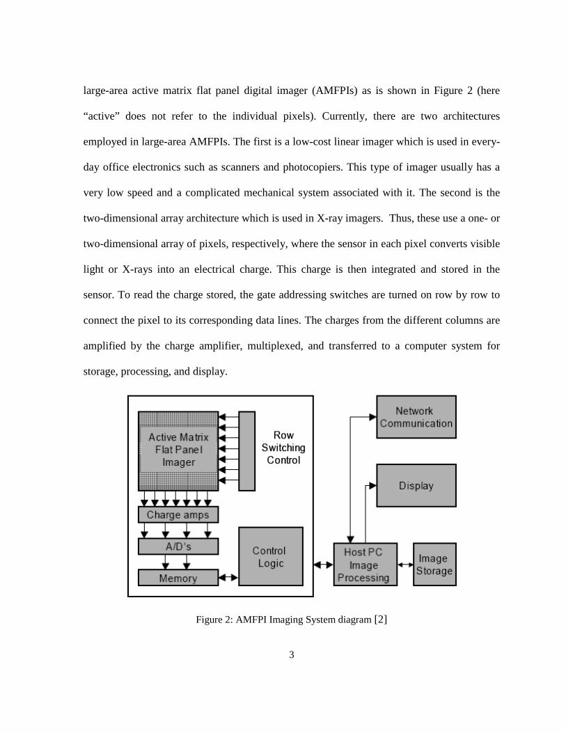
large-area active matrix flat panel digital imager (AMFPIs) as is shown in Figure 2 (here
“active” does not refer to the individual pixels). Currently, there are two architectures
employed in large-area AMFPIs. The first is a low-cost linear imager which is used in every-
day office electronics such as scanners and photocopiers. This type of imager usually has a
very low speed and a complicated mechanical system associated with it. The second is the
two-dimensional array architecture which is used in X-ray imagers. Thus, these use a one- or
two-dimensional array of pixels, respectively, where the sensor in each pixel converts visible
light or X-rays into an electrical charge. This charge is then integrated and stored in the
sensor. To read the charge stored, the gate addressing switches are turned on row by row to
connect the pixel to its corresponding data lines. The charges from the different columns are
amplified by the charge amplifier, multiplexed, and transferred to a computer system for
storage, processing, and display.
Figure 2: AMFPI Imaging System diagram [2]

4
To generate an electrical charge from an X-ray photon, two schemes are available. The first,
indirect detection, converts the X-ray photon into a visible light photon by a phosphor layer.
This visible light photon is then converted to an electrical charge by a photodetector such as a
pin diode. The second, direct detection, absorbs the X-ray and converts it directly to an
electrical charge by the X-ray photoconductor. The next subsection describes both of these
schemes and elaborates upon the need for the indirect detection.
1.4 X-ray and X-ray Detection Schemes
1.4.1 Introduction to X-ray
X-rays are a form of electromagnetic radiation with wavelengths in the range of 10 to
0.01 nm. X-rays are able to penetrate solid objects making them very useful in diagnostic
radiography. X-rays can be classified into soft X-rays and hard X-rays depend on their
energy level, which is related to its penetration ability.
X-rays are generated by using high voltages to accelerate electrons to a very high velocity
and then colliding them with a heavy metal target such as tungsten. When an electron hits the
target, an X-ray can be created through two different processes. If there is enough energy
associated with the electron to knock an electron from the inner orbit of the target metal, an
electron from a higher energy would then fill the vacancy emitting a characteristic X-ray
photon with a discrete spectrum. In the second process, the incoming electron collides with
the target metal and the radiation is given off by the electron scattering. X-rays produced this
way have a continuous spectrum.
5
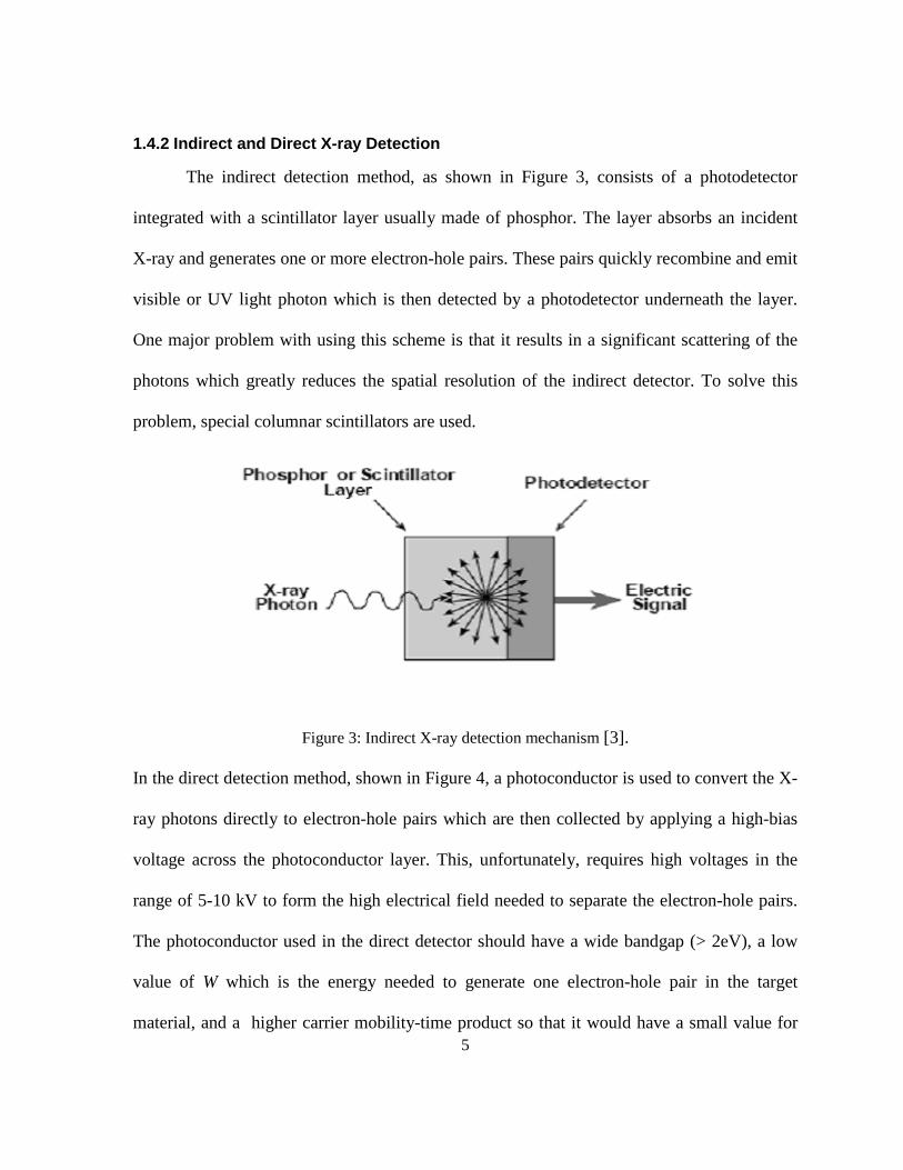
1.4.2 Indirect and Direct X-ray Detection
The indirect detection method, as shown in Figure 3, consists of a photodetector
integrated with a scintillator layer usually made of phosphor. The layer absorbs an incident
X-ray and generates one or more electron-hole pairs. These pairs quickly recombine and emit
visible or UV light photon which is then detected by a photodetector underneath the layer.
One major problem with using this scheme is that it results in a significant scattering of the
photons which greatly reduces the spatial resolution of the indirect detector. To solve this
problem, special columnar scintillators are used.
Figure 3: Indirect X-ray detection mechanism [3].
In the direct detection method, shown in Figure 4, a photoconductor is used to convert the X-
ray photons directly to electron-hole pairs which are then collected by applying a high-bias
voltage across the photoconductor layer. This, unfortunately, requires high voltages in the
range of 5-10 kV to form the high electrical field needed to separate the electron-hole pairs.
The photoconductor used in the direct detector should have a wide bandgap (> 2eV), a low
value of W which is the energy needed to generate one electron-hole pair in the target
material, and a higher carrier mobility-time product so that it would have a small value for
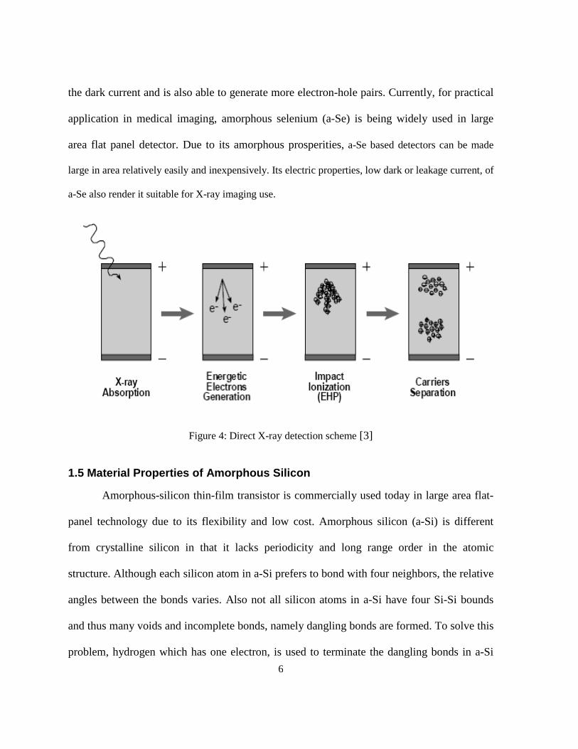
6
the dark current and is also able to generate more electron-hole pairs. Currently, for practical
application in medical imaging, amorphous selenium (a-Se) is being widely used in large
area flat panel detector. Due to its amorphous prosperities, a-Se based detectors can be made
large in area relatively easily and inexpensively. Its electric properties, low dark or leakage current, of
a-Se also render it suitable for X-ray imaging use.
Figure 4: Direct X-ray detection scheme [3]
1.5 Material Properties of Amorphous Silicon
Amorphous-silicon thin-film transistor is commercially used today in large area flat-
panel technology due to its flexibility and low cost. Amorphous silicon (a-Si) is different
from crystalline silicon in that it lacks periodicity and long range order in the atomic
structure. Although each silicon atom in a-Si prefers to bond with four neighbors, the relative
angles between the bonds varies. Also not all silicon atoms in a-Si have four Si-Si bounds
and thus many voids and incomplete bonds, namely dangling bonds are formed. To solve this
problem, hydrogen which has one electron, is used to terminate the dangling bonds in a-Si
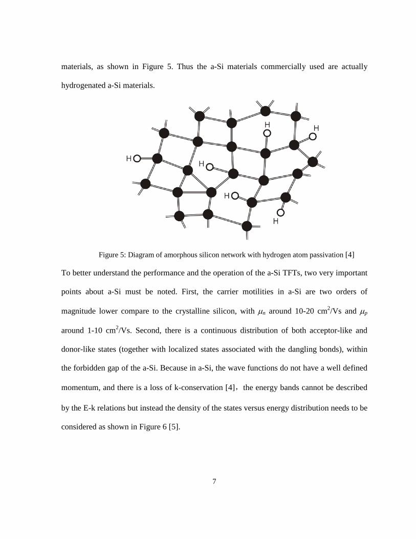
7
materials, as shown in Figure 5. Thus the a-Si materials commercially used are actually
hydrogenated a-Si materials.
Figure 5: Diagram of amorphous silicon network with hydrogen atom passivation [4]
To better understand the performance and the operation of the a-Si TFTs, two very important
points about a-Si must be noted. First, the carrier motilities in a-Si are two orders of
magnitude lower compare to the crystalline silicon, with µn around 10-20 cm2/Vs and µp
around 1-10 cm2/Vs. Second, there is a continuous distribution of both acceptor-like and
donor-like states (together with localized states associated with the dangling bonds), within
the forbidden gap of the a-Si. Because in a-Si, the wave functions do not have a well defined
momentum, and there is a loss of k-conservation [4],the energy bands cannot be described
by the E-k relations but instead the density of the states versus energy distribution needs to be
considered as shown in Figure 6 [5].

8
Ev Ec
Deep states
Tail states
Density of States
energy
Donor-like states
Acceptor-like states
Figure 6: Energy distribution versus density of state
It is clear that the density of state distribution of a-Si is asymmetric, with the conduction
band tail states having a narrower distribution than the valence band tail. The distributions of
band-tail states are given by [6]:
−=
aEcEE
tagCBag exp (1)
−=
dE
EvEtdgVBdg exp (2)

9
where gta and gtd are the densities of conduction band tail and valence band tail states,
respectively. Ea and Ed are the slopes of the conduction and valence band tails, respectively.
This together with the fact that electron mobility is higher than the hole mobility in a-Si
results in n-channel transistors being much superior compare to the p-channel counterparts.
1.5.1 Metastability
A-Si TFTs exhibit a bias-induced shift (relative to the amount of time the TFTs are
under stress) in the TFT threshold voltage VT, which can have an adverse effect on the circuit
performance if the circuit is not properly designed or operated. This problem is not
significant when the TFT is used as a switch in applications such as a liquid-crystal display
or a passive pixel sensor. However, metastability is one of the biggest challenges to
overcome when it comes to the designing of the most analog application today where the
TFTs have to withstand prolonged voltage stress on both the drain and gate terminals.
There are two mechanisms today that explain the inherent metastability associated with the
TFTs. First, the carrier (charge) trapping in the gate insulator where the high density of
defects can cause the charge to be trapped when the gate is stressed. This charge trapping in
the insulator layer causes the shift in VT. The charges are first trapped at the a-Si/SiN
interfacial layer and then travel to deeper energy states inside the a-SiN layer. The second
mechanism is explained by the point defect creation in the a-Si layer or the a-Si/SiN interface.
When electrons accumulate and form a channel at the a-Si/SiN interface, these induced
electrons are located in the conduction band tail states. These tail states are weak silicon-to-
silicon bonds, when occupied by electrons, will break and form silicon dangling bonds, in

10
other words, the induced electrons creates deep state defects. These defects again can cause
the VT of the TFT to shift.
Carrier trapping and defect creation can be distinguished: Previous studies have shown [7]
that charge trapping occurs at higher bias voltages and longer stress times. The shift in VT can
be either positive or negative depending on the type of the trapped charge (electrons or holes
respectively). Alternatively, defect state creation mechanism dominates at the lower stress
voltage and at shorter stress time. Studies done by Powell showed that defect state creation in
the lower part of the energy gap is caused by positive bias; state removal from the lower part
of the gap actually occurs for negative bias voltage [8]. Powell also determined that defect
state creation has a power law time dependence and strong dependence on temperature. In
contrast, charge trapping has logarithmic time dependence and weak dependence on
temperature. The mathematical models for the two metastability mechanism are explained in
the following paragraphs.
Defect state creation has a power law dependence over time. This relationship is empirically
determined by both Powell and Jackson [7] [9] to be
βα tVVAtV TiSTT )()( −=∆ (3)
where VST is the gate stress voltage, VTi is the VT before the stress is applied, α is unity, and β
is the experimental constant which is temperature dependent. Carrier trapping has a
logarithmic time dependence which is represented by
11
)/1log()( 0ttrtV dT +=∆ (4)
where rd is a constant and t0 is the characteristic value for time.
During the circuit operation, for the large area imagers, the gates of the TFTs are usually
under pulsed bias stress and not constant DC bias stress. A pulse is characterized by its
period and pulse width.
For positive pulse voltages, ∆VT has been widely reported to be relatively independent of
frequency. For a unipolar pulse, the effect of the frequency is just to reduce the total stress
time of the TFT. During the off cycle, negative voltage is applied to the TFT to shift the VT is
the opposite direction. A commonly accepted formula [10][11][12] for modeling the
frequency and pulse width dependence of ∆VT on positive pulse bias is given by
)()/()(_ tVTTtV TPeriodONACT++ ∆=∆ (5)
where TON is the ON time of the pulse and Tperiod is the period of the pulse. The formula for a
negative pulse bias is more complicated:
)()(_ tVktV TVACTT
−− ∆=∆ − (6)
where
−+−=−
h
ON
ON
h
ON
hV
TTT
kT τ
ττexp1 (7)
and τh is the effective hole accumulation time constant.
12
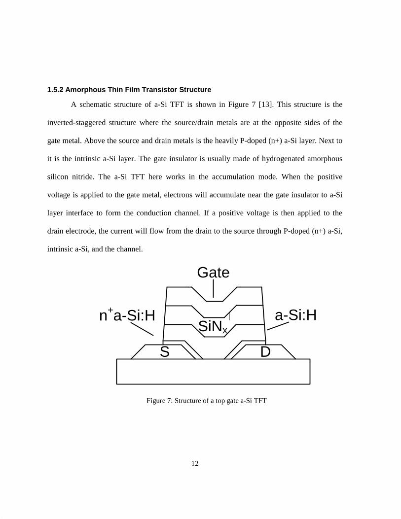
1.5.2 Amorphous Thin Film Transistor Structure
A schematic structure of a-Si TFT is shown in Figure 7 [13]. This structure is the
inverted-staggered structure where the source/drain metals are at the opposite sides of the
gate metal. Above the source and drain metals is the heavily P-doped (n+) a-Si layer. Next to
it is the intrinsic a-Si layer. The gate insulator is usually made of hydrogenated amorphous
silicon nitride. The a-Si TFT here works in the accumulation mode. When the positive
voltage is applied to the gate metal, electrons will accumulate near the gate insulator to a-Si
layer interface to form the conduction channel. If a positive voltage is then applied to the
drain electrode, the current will flow from the drain to the source through P-doped (n+) a-Si,
intrinsic a-Si, and the channel.
S D
SiNxa-Si:Hn+a-Si:H
Gate
Figure 7: Structure of a top gate a-Si TFT

13
Chapter 2 Pixel Architectures for Large Area Digital Imaging
2.1 Passive Pixel Sensor Architecture
2.1.1 Introduction
Today, the industry standard architecture for flat panel imagers is the passive pixel
sensor (PPS) [14][15]. It is probably the simplest structure and offers very compact design
for the high-resolution imaging applications. The PPS shown in Figure 8 consists of a
detector, which can be either a photo-diode integrated with a scintillator or a photoconductor,
connected to a switch transistor. Here CPIX is the sum of the sensor capacitance and parasitic
capacitances (gate to drain capacitance of the switching TFT) at the detector node. It is
passive in a sense that the TFT functions as passive switch in the pixel.
Detector
Gate Address Line
Data Line
CPIX
TFT
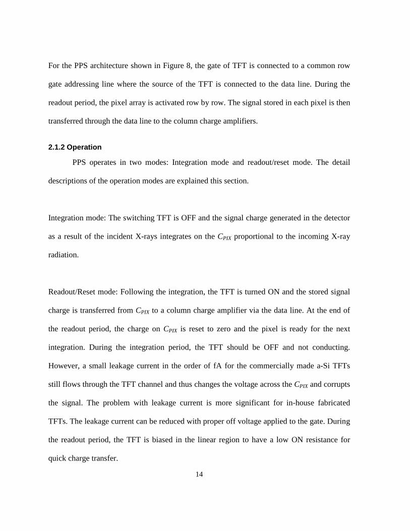
Figure 8: Passive pixel sensor architecture
14
For the PPS architecture shown in Figure 8, the gate of TFT is connected to a common row
gate addressing line where the source of the TFT is connected to the data line. During the
readout period, the pixel array is activated row by row. The signal stored in each pixel is then
transferred through the data line to the column charge amplifiers.
2.1.2 Operation
PPS operates in two modes: Integration mode and readout/reset mode. The detail
descriptions of the operation modes are explained this section.
Integration mode: The switching TFT is OFF and the signal charge generated in the detector
as a result of the incident X-rays integrates on the CPIX proportional to the incoming X-ray
radiation.
Readout/Reset mode: Following the integration, the TFT is turned ON and the stored signal
charge is transferred from CPIX to a column charge amplifier via the data line. At the end of
the readout period, the charge on CPIX is reset to zero and the pixel is ready for the next
integration. During the integration period, the TFT should be OFF and not conducting.
However, a small leakage current in the order of fA for the commercially made a-Si TFTs
still flows through the TFT channel and thus changes the voltage across the CPIX and corrupts
the signal. The problem with leakage current is more significant for in-house fabricated
TFTs. The leakage current can be reduced with proper off voltage applied to the gate. During
the readout period, the TFT is biased in the linear region to have a low ON resistance for
quick charge transfer.

15
2.1.3 Readout and Reset Speed
In this section, we will try to estimate the speed of reset and readout of the PPS
structure. The circuit diagram and small signal circuit model of a PPS pixel connected a
charge amplifier are shown in Figure 9 and Figure 10. The TFT is modeled by its overlap
capacitances and the on resistance in linear region. The pixel capacitance is given by
gdstPIX CCCC ++= det (8)
where Cdet is the detector capacitance, Cst is the pixel storage capacitance which is added if
the total capacitance at the detector node is not large enough to store the charge generated by
the incident X-rays (also reduce the voltage level at the detector node), and Cgd is the gate to
drain capacitance of the TFT.
Detector
Cdet Cst
TFT1/2Rdata 1/2Rdata
Cdata
Cf
Vout-+
PPS Data Line Charge Amplifier
Av
Cgd
Figure 9: PPS structure connecting to a column charge amplifier

16
Vout
CfAVVX-+(1+AV)Cf
VX
Cdata
½ Rdata ½ RdataRon
CgdCstCdet
Figure 10: Small signal model for a PPS structure connecting to a column charge amplifier
The data line is modeled by a line resistance and capacitance, that is, Rdata and Cdata
respectively. A zero-time constant approximation method can be used to estimate the time
constant associated with transfer of the charge from pixel capacitor to the charge amplifier
feedback capacitor. From Figure 10, the charge transfer time constant is
4/)( 222222
21 datadatadataonPIX RCRRC ++=+= τττ . (9)
The above equation can be further simplified because Ron of the TFT is considered to be
much larger than the value of Rdata and therefore
onPIX RC ×=τ . (10)
The ON resistance of the TFT in linear mode can be approximated by the equation
1
)(−
−= TGSGEFFon VVC
LWR µ . (11)
Here W and L are the channel width and length of the TFT, respectively, µEFF is the effective
carrier mobility; CG is the gate capacitance per unit area; VGS is the gate-source voltage of the
17
TFT; and VT is the threshold voltage of the TFT. The photoconductor capacitance Cdet is
given by
det
det0
tA
C P××=
εεdet (12)
where AP is the pixel area and tdet is the thickness of the photoconductor. Assuming the
photoconductor here is amorphous selenium (a-Se), typical values are ε0 = 8.85×10⁻¹²F/m,
εdet = 6.5, AP = 250×250 µm2, tdet = 1 mm would result in a value of around 3 fF for the Cdet.
If a storage capacitor of 1 pF is used, then the total pixel capacitance CPIX would be
approximately equal to 1pF. For a W/L = 160 um/20 um, µEFF = 0.5 cm2 / Vs, Von = 12 V, VT
= 2 V, CG = 25 nF/cm2, and Ron is around 1 MΩ. Thus, τ can be calculated to be around 1µs.
For a sufficient charge transfer, 5× time constants are generally needed which results in a
pixel readout time of 5 µs for each row, which is fast enough for real-time application.
However, the main disadvantage of the PPS is that it is very susceptible to the coupling noise
from various external components, making it unsuitable for low X-ray dose application such
as fluoroscopy.
2.1.4 Voltage Sensing PPS
An inverting voltage amplifier can be used instead of the charge amplifier in the PPS
structure shown in Figure 11. [2]. In this configuration, the signal charge is transferred from
CPIX to the data line capacitance, Cdata, is given by
+
×=PIXdata
datasigdata CC
CQQ.
(13)

18
In this case, if Cdata is small compared to CPIX, most of the signal charge will not be
transferred to Cdata; which will result in signal loss. In order to have good charge transfer
efficiency, it is important to have Cdata ≫ CPIX. However, if this is indeed the case, then the
voltage developed at the input of the inverting amplifier will be very small, making it
vulnerable to noise, thus not suitable for low input signals such as the ones encountered in
diagnostic medical X-ray imaging applications.
Detector
Cdet Cst
TFT1/2Rdata 1/2Rdata
Cdata
Rf
Vout-+
PPS Data Line Inverting Voltage Amplifier
Figure 11: PPS structure connecting to a column voltage amplifier
2.2 Active Pixel Sensor
2.2.1 Introduction
To improve the signal-to-noise ratio (SNR), active pixel sensor (APS) circuitry is
developed where the signal at the detector node is converted to voltage or current using an
on-pixel amplifier which results in improved noise and/or readout speed performance.
Currently, there are two common methods for reading out the signal in APS. In one method,
the output of the APS is read in terms of current (C-APS) where as in the other method the
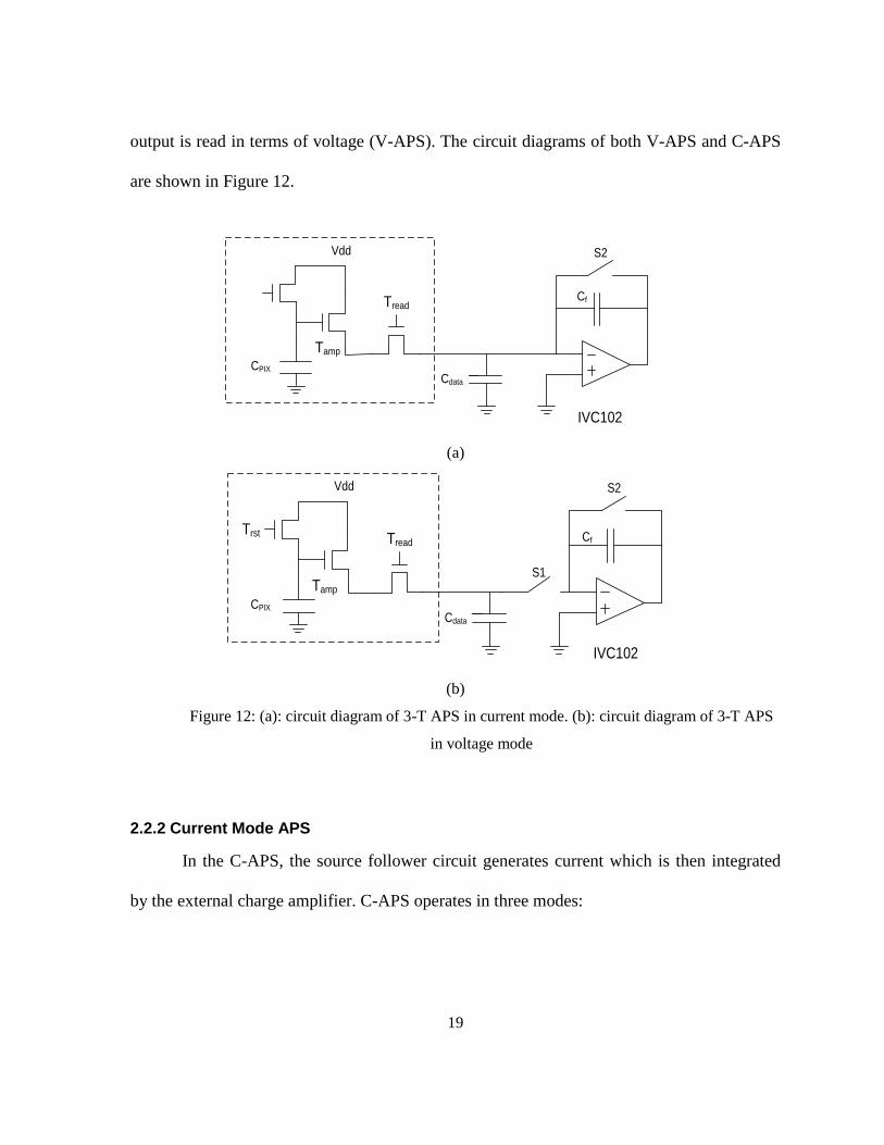
19
output is read in terms of voltage (V-APS). The circuit diagrams of both V-APS and C-APS
are shown in Figure 12.
Vdd
Cdata
S2
Cf
Tamp
Tread
IVC102
CPIX
(a)
Vdd
Cdata
S1
S2
Cf
Tamp
TreadTrst
IVC102
CPIX
(b)
Figure 12: (a): circuit diagram of 3-T APS in current mode. (b): circuit diagram of 3-T APS
in voltage mode
2.2.2 Current Mode APS
In the C-APS, the source follower circuit generates current which is then integrated
by the external charge amplifier. C-APS operates in three modes:

20
Reset mode: The reset TFT (Trst) is turned on to reset the pixel capacitor (CPIX) to the Vrst
value. CPIX is a combination of detector capacitance and the gate capacitance of the
amplifying TFT (Tamp).
Integration mode: After the CPIX node is reset to the proper value, both Trst and Tread are then
turned off. The incoming X-ray signal discharges the CPIX capacitance by ∆Q and the voltage
level on CPIX drops by ∆V that is proportional to ∆Q.
Readout mode: In the read period, Tread is turned on and the current that is generated by the
APS pixel flows into the charge amplifier. The charge amplifier then integrates this small
current on the feedback capacitor (Cf) and the output voltage (Vout) of the charge is
proportional to both ∆V and the integration time (Ts).
The small signal model for deriving the output current of C-APS is shown in Figure 13. The
output current has been derived in previous study [3] to be,
2
)(21)(1
ON
TPIXONTPIXONout KR
VVKRVVKRi
−+−−+= (14)
Where K = CGµEFFW/L of the amplifying TFT, VPIX is the voltage at the detector node after
the X-ray is absorbed which equals to Vrst – Qsig/CPIX.
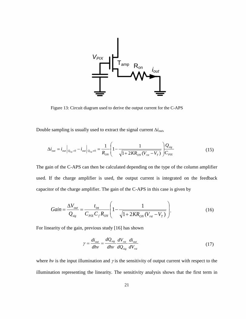
21
VPIXTamp Ron iout
Figure 13: Circuit diagram used to derive the output current for the C-APS
Double sampling is usually used to extract the signal current ∆iout,
PIX
sig
TrstONONQoutQoutout C
QVVKRR
iiisigsig
−+−=−=∆ ≠= )(21
11100 (15)
The gain of the C-APS can then be calculated depending on the type of the column amplifier
used. If the charge amplifier is used, the output current is integrated on the feedback
capacitor of the charge amplifier. The gain of the C-APS in this case is given by
−+−=
∆=
)(2111int
TrstONONfPIXsig
out
VVKRRCCt
QVGain . (16)
For linearity of the gain, previous study [16] has shown
rst
out
sig
rstsigout
dVdi
dQdV
dhvdQ
dhvdi
==γ (17)
where hv is the input illumination and γ is the sensitivity of output current with respect to the
illumination representing the linearity. The sensitivity analysis shows that the first term in

22
equation (17) is constant if the charge generated by the detector is linear with respect to the
incoming illumination. The second term is linear if the signal charge is linearly dependent on
the voltage charge, i.e.
PIXrstsig CVQ ×∆=∆ . (18)
In another word, CPIX has to be constant. For the last term in equation (17), the I-V
relationship of the TFT has to be linear,
2)(2/ TGGoutout VVVKii −∆+=∆+ . (19)
Expand and collect the small signal term gives
2))(2/()( GGTGout VKVVVKi ∆+∆−=∆ . (20)
So for linear operation, the non-linear term in equation (20) has to be sufficiently small, that
is ∆VG ≫ 2(VG – VT) which means the change in voltage at the detector node due to the X-ray
must be small. This also explains why C-APS is suitable for low dose application such as
fluoroscopy but not higher dose modalities.
One problem with non-linear pixel readout is that the correlated double sampling mechanism
cannot be performed using hardware as it is typically done with active matrix imagers [2]. A
couple of methods can be used to improve the inherent nonlinearity of the C-APS. A possible
solution is to implement software correction, where a frame memory is used to store each C-
APS pixel’s transfer function so the nonlinearity can be corrected. However this means a
longer frame time is required to make all the gain adjustments. To make this software
23
correction even more complicated, the inherent VT shift problem associated with TFTs will
cause the pixel transfer characteristics to shift. This again requires repeated correction of the
pixel transfer function at regular basis which further increases the readout time associated
with the imager. In section 2.4, a hybrid pixel architecture based on PPS and C-APS is
introduced which can operate in both PPS mode and APS mode. It offers on-pixel gain, fast
readout, and high dynamic range depending on the mode it operates in.
One thing to consider when using a charge amplifier is to ensure that the bias current does
not saturate the charge amplifier. Usually the feedback capacitor of the charge amplifier is
chosen to be very small in order to have higher gain. For example, a particular charge
amplifier with 1 pF feedback capacitor and maximum output voltage of 15 V will get
saturated in 10 µs if the bias current is 1.5 µA. To prevent this problem, a current sink
circuitry or current bleeder can be used as shown in Figure 14.
As mentioned in section 2.1.4, a trans-impedance amplifier can also be used instead of a
charge amplifier. In this case, the gain of C-APS becomes
−+−=
∆=
)(2111
TrstONONPIX
f
sig
out
VVKRRCR
QVGain . (21)
24
Currentsink
Vdd S2
Cf
Tamp
Tread
Vout
IVC102
Cpixel
Figure 14: C-APS with column current sink
2.2.3 Voltage Mode APS
The circuitry for V-APS is very similar to the C-APS except one extra switch (see
Figure 12 b). V-APS also operates in three modes:
Reset mode: The reset TFT (Trst) is turned on to reset the pixel capacitor (CPIX) to the proper
Vrst value.
Integration mode: After the CPIX node is reset to the proper value, both Trst and Tread are then
turned off. The incoming X-ray signal discharges the CPIX capacitance by ∆Q and the voltage
level on CPIX drops by ∆V that is proportional to ∆Q.
Readout: There are two phases in the readout period for V-APS. In the first phase, S1 is open,
S2 is closed, and Tread is turned on so the small current generated by the APS pixel is flowing
to the data line capacitor (Cdata) until it is charged up to Vg – VT of the two-transistor structure
consist of Tamp and Tread. The time required to charge up the Cdata depends on the size of Cdata
25
and resistance of Tread. In the second phase, S1 is closed, S2 is open, and Tread is turned off.
The charge stored on the Cdata instantly transfers to the Cf and the output voltage is developed.
The output voltage of the V-APS is approximated by
+××=
f
datav
PIX
sigout C
CA
CQ
V 1 . (22)
Here Av is the voltage gain from detector node to the data line node Vdata and can be assumed
to be unity. So the gain of the V-APS is then given by
+==
f
data
PIXsig
out
CC
CQV
Gain 11 . (23)
2.3 Two-Transistor Pixel Architecture
The three-transistor APS architectures introduced in sections 2.2.2 and 2.2.3 have
good noise performance, fast readout. However, for some specific applications such as
mammography where very high resolution images are required, the pixel size (~50 µm)
becomes a challenge for the existing three-transistor APS structure. The two-transistor (2T)
APS has been proposed to address this challenge by reducing the number of both transistor
and control lines. Currently there are three different types of 2T APS: gate switching, drain
switching, and source switching.
2.3.1 Gate Switching 2T APS
The 2T gate switching APS architecture is shown in Figure 15 [3]. It consists of an X-
ray detector, a reset TFT, TR, which is used to reset the detector node to proper value, an
amplifying TFT, TA, which is used to provide on-pixel amplification, and a pixel capacitor

26
CPIX, which is used to store the charge produced by the detector while also provides access to
the gate of amplifying TFT.
Detector
CPIX
Read
Reset TR
TA
Output
Vbias
Figure 15: Gate switching 2T APS
Similar to the three-transistor APS, gate switching 2T APS also operates in three modes as
shown in Figure 16: resetting, integration, and readout. In the resetting mode, TR is turned on
and TA is turned off to reset the voltage at the detector node to zero by discharging node to
the ground. During the integration mode, both TA and TR are kept off and the detector node
voltage is modulated by the charged generated by the detector. In the readout mode, a pulse
is applied to the read node which is capacitively coupled to the gate of the TA by the pixel
capacitor, CPIX. This in turn increases the gate-source voltage of TA beyond its threshold
voltage while preserving the charge at the gate, which provides a non-destructive readout.
The total number of input/output lines for this architecture is four.
27
Read
Reset
Output 0 0 Iout
TA-TR OFF-ON OFF-OFF ON-OFF
Resetting Integration Readout
Figure 16: Operation modes for 2T gate switching APS [3]
2.3.2 Source Switching 2T APS
The second configuration for 2T APS is the source switching APS, which is shown in
the Figure 17. In this architecture, the read control line is connected to the source of the TA
instead of the CPIX in the case of gate switching. Total number of input/output lines for this
architecture is five, which is one more compare to the 2T gate switching APS
TA
Detector
CPIX
Read
Reset TR
Output Figure 17: Source switching 2T APS [3]

28
The circuit also works in the same three operation modes (Figure 18) as the 2T gate
switching APS. In the reset mode, TR is turned on to reset the detector node to a preset
voltage VRST, which is controlled by the drain voltage of the TA. TA is kept off during the
reset period because both the drain and the source of the TFT are kept high. During the
integration period, the signal charge created by the detector will change the voltage level at
the detector node. Both TFT in this period are kept in the off state. In the readout period, the
source voltage is set to zero, which turns on the TA by making its Vgs to be positive. One
thing to notice is that the source of the TA is actually capacitively coupled to its gate through
the parasitic capacitance Cgs. So when the source of TA is switched from Vbias to zero, there
will be a voltage drop of eff
gsbias C
CV × on its gate where Ceff is approximated equal to Cgs + CPIX.
In conclusion, CPIX must be sufficiently large compare to the Cgs in order to have large Vgs on
TA in readout period. This in turn requires a large physical space for a large CPIX.
Read
Reset
Output High High Iout
TA-TR OFF-ON OFF-OFF ON-OFF
Resetting Integration Readout
Figure 18: Operation modes for 2T source switching APS [3]

29
2.3.3 Drain Switching 2T APS
The third type of 2T APS is the drain switching configuration which is shown in
Figure 19. In this architecture, the drain and the gate of the TA are capacitively coupled by
the pixel capacitor CPIX. One advantage of this design is that the CPIX can simply be made by
extending the gate-drain overlap area of TA, which saves additional pixel space. This
configuration has only three input/output lines, which is the fewest among all the 2T APS
introduced in this section. The operation modes of drain switching and gate switching APS
are very similar (Figure 20). During the reset period, TR is turned on to reset the detector
node to zero. During the integration period, TA is kept off since both its drain and the source
voltage are kept at zero. For readout, the read signal Vread is applied directly to the drain of
the TA which also increase the gate voltage of TA by eff
PIXread C
CV × where Ceff is approximately
equal to gdPIX CC + (TA). One of the advantages of this architecture is that during the
integration period, the gate, drain, and source of the TA are kept at low voltage which
prevents the VT shift of the TFT from happening.
Detector
Cpix
TA
TR
Read
Reset
Output
30
Figure 19: Source switching 2T APS [3]
Read
Reset
Output 0 0 Iout
TA-TR OFF-ON OFF-OFF ON-OFF
Resetting Integration Readout
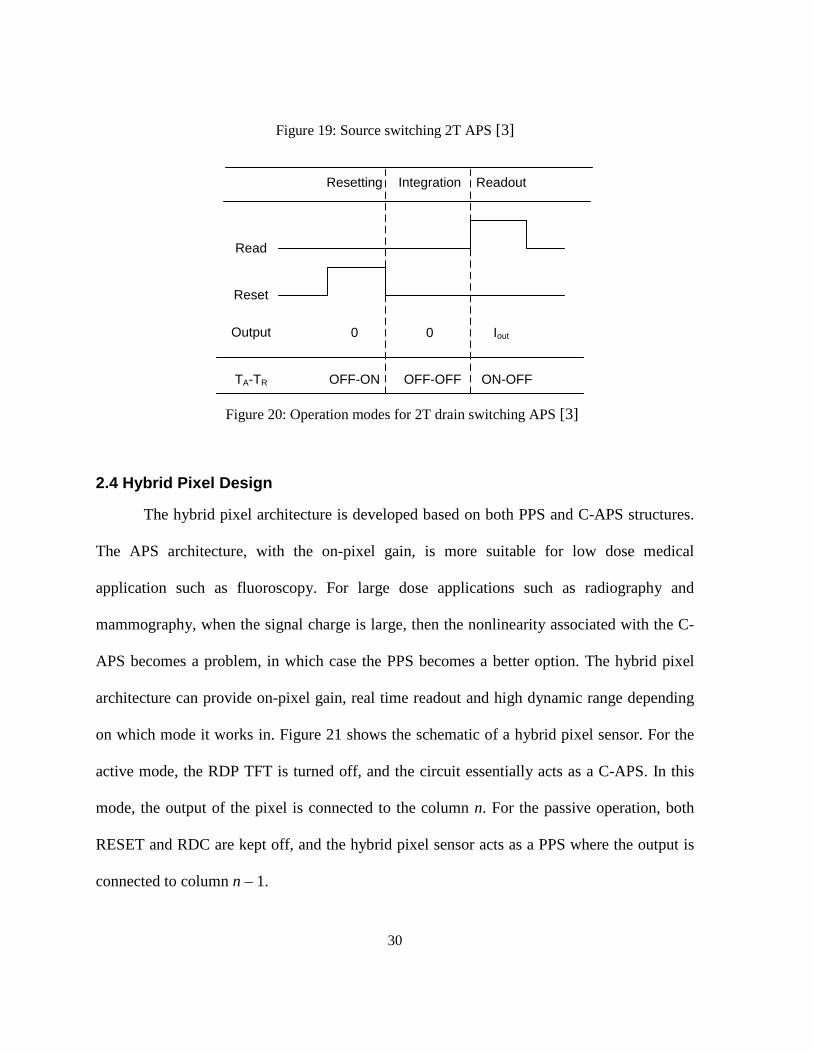
Figure 20: Operation modes for 2T drain switching APS [3]
2.4 Hybrid Pixel Design
The hybrid pixel architecture is developed based on both PPS and C-APS structures.
The APS architecture, with the on-pixel gain, is more suitable for low dose medical
application such as fluoroscopy. For large dose applications such as radiography and
mammography, when the signal charge is large, then the nonlinearity associated with the C-
APS becomes a problem, in which case the PPS becomes a better option. The hybrid pixel
architecture can provide on-pixel gain, real time readout and high dynamic range depending
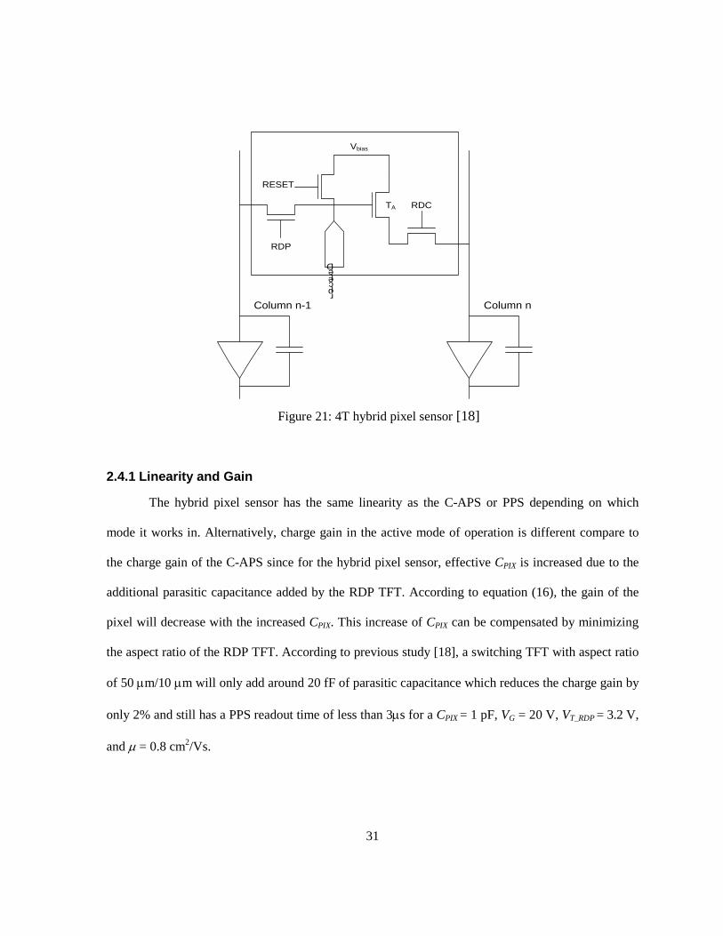
on which mode it works in. Figure 21 shows the schematic of a hybrid pixel sensor. For the
active mode, the RDP TFT is turned off, and the circuit essentially acts as a C-APS. In this
mode, the output of the pixel is connected to the column n. For the passive operation, both
RESET and RDC are kept off, and the hybrid pixel sensor acts as a PPS where the output is
connected to column n – 1.
31
Detector
RDP
RDC
RESET
TA
Column n-1 Column n
Vbias
Figure 21: 4T hybrid pixel sensor [18]
2.4.1 Linearity and Gain
The hybrid pixel sensor has the same linearity as the C-APS or PPS depending on which
mode it works in. Alternatively, charge gain in the active mode of operation is different compare to
the charge gain of the C-APS since for the hybrid pixel sensor, effective CPIX is increased due to the
additional parasitic capacitance added by the RDP TFT. According to equation (16), the gain of the
pixel will decrease with the increased CPIX. This increase of CPIX can be compensated by minimizing
the aspect ratio of the RDP TFT. According to previous study [18], a switching TFT with aspect ratio
of 50 µm/10 µm will only add around 20 fF of parasitic capacitance which reduces the charge gain by
only 2% and still has a PPS readout time of less than 3µs for a CPIX = 1 pF, VG = 20 V, VT_RDP = 3.2 V,
and µ = 0.8 cm2/Vs.
32
Chapter 3 Noise Analysis of Current Mode and Voltage Mode APS
3.1 Introduction
In this section, we first introduce the concept of the electronic noises in circuits. Then
we present the theoretical noise analysis for both readout methods: C-APS and V-APS. TFT
leakage noise, circuit thermal noise, circuit flicker noise, data line noise and the charge
amplifier noise are considered. Other noise sources such as photoconductor shot noise,
transistor leakage noise, reset noise are not included in this study partially due to the fact
these noise sources are common to both readout methods. Both the photoconductor shot
noise and transistor leakage noise are under 100 electrons and the reset noise associated with
the APS is around 400 electrons according to previous study [25].
3.2 Introduction to Electrical Noise
The noise analysis done in this thesis study deals only with the electrical noise caused
by small current and voltage fluctuations that are generated by the electronic devices.
3.2.1 Thermal Noise
In electronic devices, thermal noise is generated by the random motion of electrons
and it is directly proportional to the temperature. For a resistor R, the thermal noise can be
represented by either a voltage source or a current source:
fkTRv ∆= 42 (24)
33
fR
kTi ∆=142 (25)
where k is Boltzmann’s constant, T is the temperature in kevin, and ∆f is the bandwidth.
For a long channel MOS transistor, because the channel material is resistive, the thermal
noise can be represented by a current noise source between the drain and source, that is
( ) fgmkTid ∆= γ42 (26)
where γ is a parameter for the transistor that has a value of 1 in the linear region and 2/3 in
the saturation region.
For TFT, studies done by Boundry, Antonuk, and Karim [19][20] have shown that thermal
noise in TFT is similar to MOS transistor thermal noise and can be modeled by equation (26)
where gm in this case is
nTGS
DS
DS VVMdVdIgm )( −== (27)
where n is a process dependent parameter and
=
LWCM GEFFµ . (28)
3.2.2 Flicker Noise
Flicker noise is caused by the traps associated with the defects in the crystal structure
of the devices. It is always associated with the direct current and has the current spectral
density of the form

34
ffIKi b
a
∆=2 (29)
where K is a constant associated with a particular device, f is the frequency, a is a constant in
the range between 0.5 to 2 [21], and b lies between 0.8 and 1.4 in general [2]. If b is unity,
then the noise spectral density has a 1/f frequency dependency (hence the name 1/f noise).
Thus the flicker noise is most significant in the lower frequency range and at higher
frequencies it is usually overshadowed by the thermal noise.
Two different theories which explain the origin of the flicker noise have been developed
since its discovery. The first model, which is called the numbers fluctuation model, was
proposed by McWhorter [22]. The model states that the cause of the noise is due to the
fluctuations in the majority carrier density and interface trap density close to the
semiconductor surface. The model, however, does not account for the flicker noise observed
in materials that have no interface traps
The second theory was proposed by Hooge and Hoppenbrouwers in the 1960s and is
generally known as the mobility fluctuation model [23]. The theory explains the cause of the
flicker noise is the mobility fluctuations within a homogenous and conducting medium.
Hooge proposed the empirical formula for the noise current power spectral density:
)/(22 atotH fNIi α= (30)

35
for the transistor where I is the drain current of the transistor, Ntot is the total number of
charge carriers in the medium and Hα is the empirical coefficient. The value of this
coefficient is dependent on the impurity scattering in a material [24].
The flicker noise densities derived from both theories for TFT are listed in the Table 1 where L is the
channel length and VT is the threshold voltage.
Table 1: Flicker noise spectral densities for number fluctuation and mobility fluctuation
models for TFT
Number fluctuation model Mobility fluctuation model 2lineari ( )( )21
2 DSn
TGSOX
VVVMLCf
k −−µ ( )( )2
2 DSn
TGSH VVVM
Lq
f−
µα
2saturationi ( )( )1
2+− n
TGSOX
VVMLCf
k µ ( )( )22
+− nTGS
H VVMLq
fµα
The experimental results from this study, which are presented in the section 4.1.2, show that
the Hooge theory of flicker noise accounts for our in-house fabricated a-Si TFTs.
3.3 Noise in Current Mode APS
The analysis here for the C-APS is a modification of previous work from our group
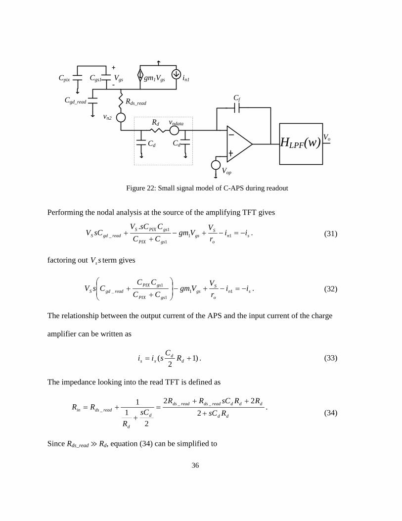
[25]. Figure 22 shows the small signal model used for the noise analysis. The read TFT is
modeled by its drain to source resistance. The input capacitance of the charge amplifier is
ignored since it is connected to the negative input of the charge amplifier which is the virtual
ground in this configuration.
36
HLPF(w)
Cpix Cgs1
+
-Vgs gm1Vgs in1
Cgd_read Rds_read
vn2 Rd vndata
Cd Cd
Vop
Cf
Vo
Figure 22: Small signal model of C-APS during readout
Performing the nodal analysis at the source of the amplifying TFT gives
sno
Sgs
gsPIX
gsPIXSreadgdS ii
rV
VgmCCCsCV
sCV −=−+−+
+ 111
1_
.. (31)
factoring out sVs term gives
sno
Sgs
gsPIX
gsPIXreadgdS ii
rV
VgmCC
CCCsV −=−+−
++ 11
1
1_ . (32)
The relationship between the output current of the APS and the input current of the charge
amplifier can be written as
)12
( += dd
xs RC
sii . (33)
The impedance looking into the read TFT is defined as
dd
dddreaddsreadds
d
d
readdsin RsCRRsCRR
sCR
RR+
++=
++=
222
21
1 ___ .
(34)
Since Rds_read ≫ Rd, equation (34) can be simplified to

37
readdsdd
ddreadds
dd
ddreaddsreaddsin R
RsCRsCR
RsCRsCRR
R ____
2)2(
22
=+
+≈
+
+≈ . (35)
We then write Vgs in term of VS, that is
111
1 1
gsPIX
PIXS
gsgsPIX
gsPIXSgs CC
CVsCCC
CsCVV
+−
=
+
−= (36)
and
readdssS RiV _= . (37)
Substitute equation (36) and (37) into (32),
sno
readdss
gsPIX
PIXreaddss
gsPIX
gsPIXreadgdreaddss ii
rRi
CCC
RigmCC
CCCRsi −=−+
++
++ 1
_
1_1
1
1__
(38)
Re-arrange the equation and substitute equation (33) in,
1_
1_1
1
1__ 11
2 no
readds
gsPIX
PIXreadds
gsPIX
gsPIXreadgdreaddsd
dx i
rR
CCCRgm
CCCC
CsRRC
si =
++
++
++
+
Now we can relate the output voltage with the ix,
fox sCVi −= (39)
Finally, we find the relationship between the noise source in1 and the output voltage Vo,
1_
1_1
1
1__ 11
2 no
readds
gsPIX
PIXreadds
gsPIX
gsPIXreadgdreaddsd
dfo i
rR
CCCRgm
CCCC
CsRRC
ssCV =
++
++
++
+−
(40)
Further simplification can be made to equation (40). First of all, the term o
readds
rR _ can be
ignored since ro ≫ Rds_read. Now expand the equation (40),
38
( )1
1
1_11_1__ )(1
2 ngsPIX
gsPIXPIXreaddsgsPIXreaddsgsPIXreadgdreaddsd
dfo i
CCCCCRgmCCsRCCCsR
RCssCV =+
+++++
+−
(41)
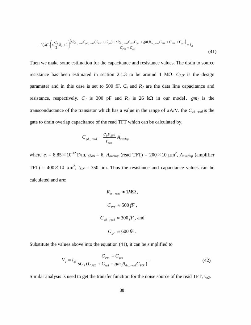
Then we make some estimation for the capacitance and resistance values. The drain to source
resistance has been estimated in section 2.1.3 to be around 1 MΩ. CPIX is the design
parameter and in this case is set to 500 fF. Cd and Rd are the data line capacitance and
resistance, respectively. Cd is 300 pF and Rd is 26 kΩ in our model. gm1 is the
transconductance of the transistor which has a value in the range of µA/V. the Cgd_read is the
gate to drain overlap capacitance of the read TFT which can be calculated by,
overlapSiN
SiNreadgd A
tC
εε 0_ =
where ε0 = 8.85×10⁻¹² F/m, εSiN = 6, Aoverlap (read TFT) = 200×10 µm2, Aoverlap (amplifier
TFT) = 400×10 µm2, tSiN = 350 nm. Thus the resistance and capacitance values can be
calculated and are:
Ω≈ MR readds 1_ ,
fFCPIX 500≈ ,
fFC readgd 300_ ≈ , and
fFCgs 6001 ≈ .
Substitute the values above into the equation (41), it can be simplified to
)( _11
11
PIXreaddsgsPIXf
gsPIXno CRgmCCsC
CCiV
++
+= . (42)
Similar analysis is used to get the transfer function for the noise source of the read TFT, vn2.

39
Now let’s consider the noise coming from the data line (Figure 22), which is modeled using a
π model composed of a line resistor and two line capacitors. Performing nodal analysis again
gives
1
2d
d
ndatax
Cs R
v i
+
=
(43)
and
fxo sC
iV 1= . (44)
Solving (44) for ix and substituting it into (43), we get
fodd
dndata
sCVsCR
sCv
=+
21
2 . (45)
Solve for Vo, we get
fdd
dndatao CsCR
CvV
)2( += . (46)
The transfer functions of various noise sources referred to the output node are given by the
three equations
)( _11
1
1 pixreaddsmgspixf
gspix
n
o
CrgCCsCCC
iV
++
+= , (47)
)( _11
1
2 pixreaddsgspixf
pix
n
o
CrgmCCsCCgm
vV
++= , (48)

40
fdd
d
ndata
o
CSCRC
vV
)2( += . (49)
Since the noise sources are independent and uncorrelated, the total thermal noise at the
output node of the charge amplifier from the two transistors is given by
dfHCrgmCCsC
CCiCgmvV LPFpixTsgspixf
pixgsnpixnthermalo )()(
1)()( 2
2
11
21
21
21
22
2, ω∫ ++
++=
(50)
where )(2 ωLPFH is low pass filter associated with the data acquisition system connected to
output of the charge amplifier. The thermal noise sources are given by
= 1
21 3
24 gmkTin (51)
and
readdsn kTRv _22 4= . (52)
For flicker noise, the thermal noise densities can be replaced with the flicker noise densities.
Hooge’s model for the flicker noise current spectral density in both linear and saturation
regimes is given by [26][27],
3
22
,
)(fL
VVVWCqi DSTGSoxeffH
flinear
−=
µα (53)
3
32
, 2)(
fLVVWCq
i TGSoxeffHfsat
−=
µα (54)
For the charge amplifier noise, refer to the small signal model shown in Figure 23.
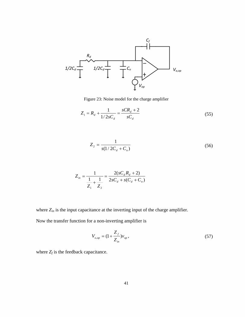
41
Vop
Cf
Rd
1/2Cd 1/2Cd Cn Vo,op
Figure 23: Noise model for the charge amplifier
d
d
dd sC
sCRsC
RZ2
2/11
1+
=+= (55)
)2/1(1
2nd CCs
Z+
= (56)
)(2)2(2
111
21
ndd
ddin CCssC
RsC
ZZ
Z+++
=+
=
where Zin is the input capacitance at the inverting input of the charge amplifier.
Now the transfer function for a non-inverting amplifier is
opin
fopo v
ZZ
V )1(, += , (57)
where Zf is the feedback capacitance.

42
opdd
ddndd
fopo v
RsCRsCCCssC
sCV
+
++++=
)2(2)2)((211.
which simplifies to
(58)
opddf
nddnddddopo v
RsCCCRCsCCRsCC
V
+++++
+=)42(
2221
2
, . (59)
Now, since 2sCdRd ≪ 4, equation (59) can be simplified to
opf
fndddnddopo v
CCCCRCCRCs
V
++++
≈4
424)( 2
, . (60)
Using the same assumption made on page 38, finally we get
opf
fnd
opo vC
CCCV
++= 2
1
, . (61)
So the charge amplifier output noise voltage is given by
dfHC
CCCVV LPF
f
fnd
opopo )(21
2
2
22, ω
++= (62)
where Vop2 is the charge amplifier noise voltage and is given by
22 1 thc
op VffV
+=
(63)
and Vth2 is the thermal noise density and fc is the corner frequency of the charge amplifier.
43
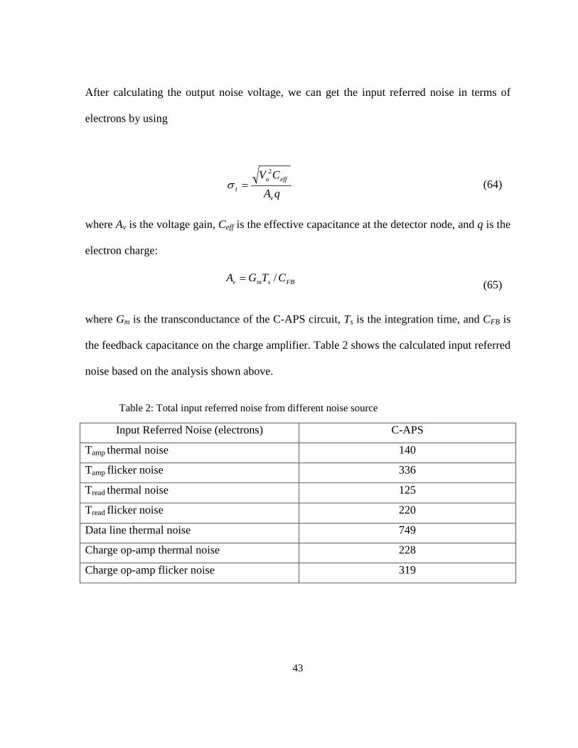
After calculating the output noise voltage, we can get the input referred noise in terms of
electrons by using
qACV
v
effot
2
=σ (64)
where Av is the voltage gain, Ceff is the effective capacitance at the detector node, and q is the
electron charge:
FBsmv CTGA /= (65)
where Gm is the transconductance of the C-APS circuit, Ts is the integration time, and CFB is
the feedback capacitance on the charge amplifier. Table 2 shows the calculated input referred
noise based on the analysis shown above.
Table 2: Total input referred noise from different noise source
Input Referred Noise (electrons) C-APS
Tamp thermal noise 140
Tamp flicker noise 336
Tread thermal noise 125
Tread flicker noise 220
Data line thermal noise 749
Charge op-amp thermal noise 228
Charge op-amp flicker noise 319
44
3.4 Noise in Voltage Mode APS
For the V-APS, Figure 24 shows the equivalent small signal circuit of the pixel
during readout mode. In the first phase of the readout period, the data line capacitor will
eventually get charged up to Vgs – VT of the Tamp and when this steady state is reached, the
direct current flowing through the transistors is assumed to be zero. The only noise present is
the thermal noise which is stored on the Cdata, given by
datan C
kTV =2
. (66)
In the second phase of the readout period (Figure 24b), the noise stored on the Cdata is then
transferred to the output node of the charge amplifier. The noise gain function is given by,
2,
2thermalon VV β= (67)
where
f
data
CC
+=11β
(68)
so the thermal noise at the output of the charge amplifier is given by
dataf
datathermalo C
kTC
CV2
2, 1
+=
. (69)
One interesting point here is that the output referred noise is proportional to the data line
capacitance Cdata. Assume Cdata ≫ Cf, equation (69) can be simplified to
f
data
dataf
datathermalo C
CCkT
CC
V ∝≈, . (70)

45
Assuming that the feedback capacitance is constant; a large data line capacitance would give
you higher output referred noise according to equation (70). Now let us consider the input
referred noise
PIX
data
f
data
PIX
dataf
data
thermalothermalreferredinput
C
CkT
CC
C
CkT
CC
gainV
V1
11
1,
__ =
+
+
== . (71)
Again, assume that Cdata ≫ Cf, and CPIX and Cf are design constant, we can deduce the
relationship
datathermalreferredinput C
V 1__ ∝ (72)
between the input referred noise and the data line capacitance. This shows that the input
referred noise of the V-APS is actually inversely proportional to the square root of the data
line capacitance.
rdsamp rdsread Rdata
Cdata
Cd
Vop
Cf
V
Vo
(a) (b)
Figure 24: Small signal model of V-APS during (a) Phase 1 of the readout, and (b) Phase 2 of the readout.
The total input referred noise for V-APS is calculated and summarized in Table 3.

46
Table 3: Total input referred noise from different noise source
Input Referred Noise (electrons) C-APS
kT/C noise 12
Charge op-amp thermal noise 228
Charge op-amp flicker noise 319
The analysis in this chapter shows that the V-APS has a substantial advantage in term of
input referred noise. At the same time it is also shown that the noise in V-APS is independent
of the bias voltage for the APS structure, which is another advantage over C-APS.

47
Chapter 4 Noise Measurement
In this chapter, the measurement setup and the measurement results for both single
TFT and APS are presented.
4.1 Noise Measurement of a Single TFT
4.1.1 Measurement Setup
The current noise power spectrum measurements are performed on a single TFT
fabricated at the University of Waterloo with the aspect ratio of 400 µm/20µm. The setup for
measuring the noise of a single a-Si TFT is shown in Figure 25. High amp hour DC batteries
are used to drive the TFT and also to provide the power for the PerkinElmer Model 5182
low-noise current preamplifier. The TFT, batteries, low noise capacitors and low noise
resistors are put in a shielded box and the entire system excluding the spectrum analyzer is
placed in the Faraday cage. In this setup, a capacitance is used to block the DC current from
entering the low noise current preamplifier. This protects the current preamplifier and at the
same time also allows us to use the highest gain setting on the current preamplifier. The noise
current, which is AC in nature, will flow into the current preamplifier since the input
impedance of a current amplifier is much smaller compare to the drain resistance of the TFT
under test.

48
Low noise current preamplifer Spectrum Analyzer
battery
battery
battery
R
TFT
Ccoupling
Figure 25: Noise experiment setup for a single TFT
The gate voltage and drain voltage are set to be 15 V and 2 V, respectively. The current noise
power spectrum is constructed from narrowband measurement averaged at last 50 times and
higher for low frequency measurements. For each measurement, the data acquisition starts
after a 15 minutes delay to allow the VT shift of the TFT to stabilize. The bias current is
monitored at the same time as the noise spectrum measurements are taken.
4.1.2 Flicker Noise
The noise current power spectral density of one single TFT is measured using the
aforementioned experimental setups and are shown in Figure 26.

49
1.00E-28
1.00E-27
1.00E-26
1.00E-25
1.00E-24
1.00E+01 1.00E+02 1.00E+03 1.00E+04
Frequency (Hz)
SID (A2/Hz)
VG = 15 V
VD = 2 V
(a)
1.00E-26
1.00E-25
1.00E-24
1.00E+01 1.00E+02
Frequency (Hz)
SID (A2/Hz)
VG = 15 V
VD = 2 V
(b)
Figure 26: Noise current power spectral density for an a-Si TFT in the linear mode. (a): Noise spectra ranges from 10 Hz to 1 MHz. (b): Noise spectra in low frequency range (10 Hz to
100 Hz). From the mobility fluctuation equation list in Table 1 in section 3.2.2, it is clear that
nTGSlinear VVi )(2 −∝ . (73)
Also for a transistor in the linear region
nTGSlineard VVi )(, −∝ . (74)
Then

50
lineardlinear ii ,2 ∝ (75)
Figure 27 shows measurements of the noise power spectrum at 100 Hz. The current noise
power spectral density is shown to be proportional to the drain current with a slope of 0.9
which indicates that the flicker noise associated with the in-house fabricated TFTs appears to
concur with the mobility fluctuation theory.
Figure 27: Bias current vs. current power spectral density.

51
4.2 Noise Measurement for C-APS and V-APS
4.2.1 Test Structure and Measurement Setup
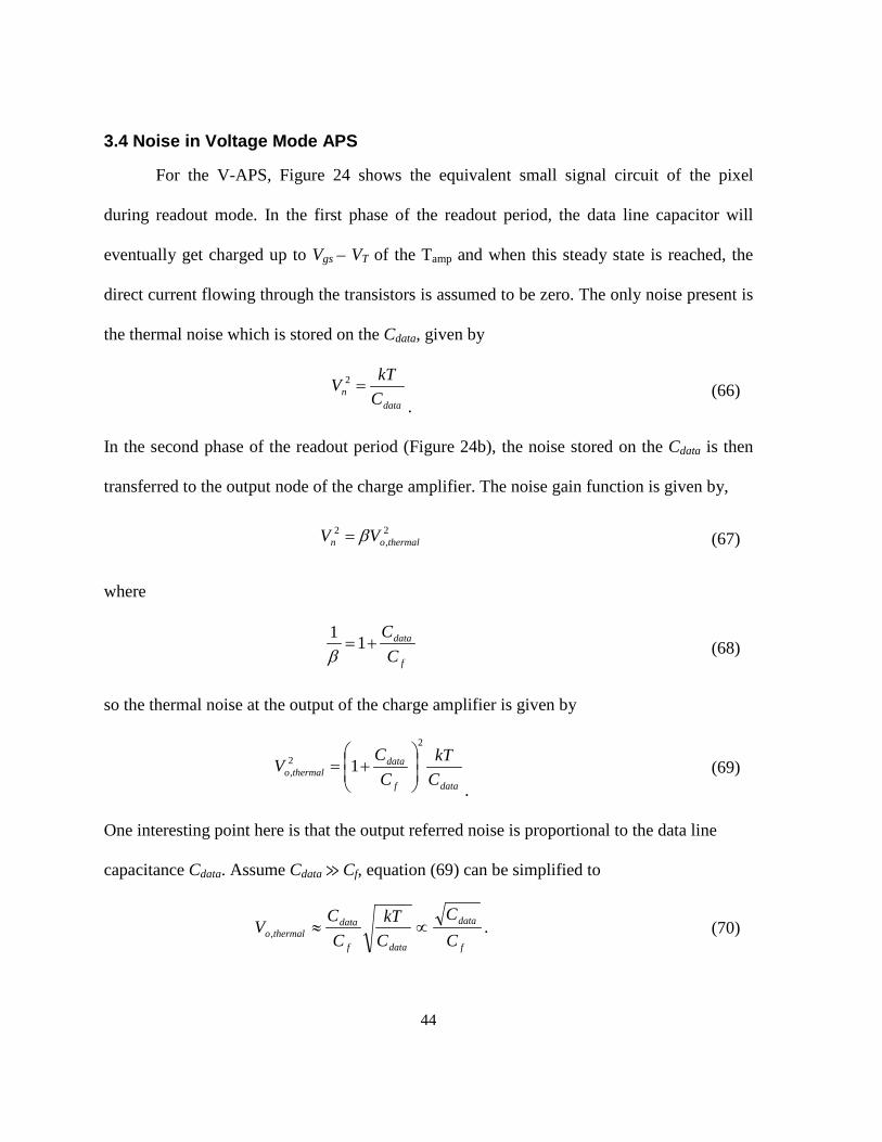
The APS pixel architectures used in this study are shown in Figure 28. The reason we
do not include Trst in our analysis is because the reset operation is common to both current
and voltage mode APS circuits, thus the reset noise associated is the same for both modes of
the operation. The a-Si TFTs used in this study were fabricated in-house at the University of
Waterloo. Tamp and Tread have W/L ratios of 400 µm/20 µm and 200 µm/20 µm, respectively.
The pixel storage capacitance is designed to be 0.5 pF. The line capacitance Cdata is modeled
by using a 400 pF discrete capacitor. Notice this is an over-estimation of the data line
capacitance for the worst case scenario. This is also one of the major reasons why the noise
measurement results presented in this study are higher than the theoretical calculations. The
charge amplifier used here is the low noise IVC 102 with the built-in feedback capacitor set
to be 30 pF.
Vdd
Cdata
S1
S2
Cf
Tamp
Tread
Vout
IVC102
(a)
52
(b)
Figure 28: (a) Circuit diagram of the device under test (DUT). (b) Micrograph of the in-house
fabricated 3 TFT structure
The experimental setup is shown in Figure 30. It consists of a Wavetek model 195 universal
wave generator and a National Instrument 6115 data acquisition card (NI card). Voltage
buffers powered by batteries are used to reduce the output noise from the wave generator.
The system is placed in a Faraday cage and the measurements are recorded under dark
conditions at room temperature. Two hundred samples were used for each output noise
variance calculation.
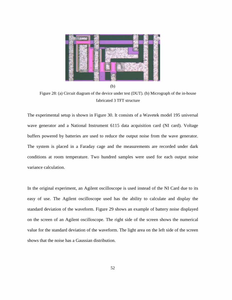
In the original experiment, an Agilent oscilloscope is used instead of the NI Card due to its
easy of use. The Agilent oscilloscope used has the ability to calculate and display the
standard deviation of the waveform. Figure 29 shows an example of battery noise displayed
on the screen of an Agilent oscilloscope. The right side of the screen shows the numerical
value for the standard deviation of the waveform. The light area on the left side of the screen
shows that the noise has a Gaussian distribution.
53
Figure 29: noise of a dc battery displayed on the Agilent oscilloscope
Unfortunately, the maximum resolution of the ADC in this oscilloscope is only 10 bits,
which is not sufficient for the proposed study.
54
DUT
Voltage Buffer
Pulse Generator
NI Card
(a)
Vdd (battery)
Cdata
S1
S2
Cf
Tamp
Tread
NI Card
IVC102
Wavetek 195 generator
Voltage Buffer
Voltage Buffer
Voltage Buffer
Voltage Buffer
(b)

55
Computer with National
Instrument 6115 data
acquisition card installed
National Instrument Interface
Card
Agilent oscilloscope
(c)

56
Copper Box
Wavetek model 195 universal wave
generatorDC power supply
(d)
Figure 30: Experimental set-up used to measure the output noise (a) block diagram. (b) detailed
schematic. (c) test setup including NI card and oscilloscope (d) test setup including the
Wavetek universal wave generator
The noise measurements are performed using the setup discussed in this section. The detailed
experiment results are presented in the next two sections.
4.2.2 Measurement Results for C-APS
The timing diagram and the output wave form for the C-APS is showing in Figure 31
and Figure 32. The period of the signal is 100 µs and the magnitude of the output voltage
decreases from around 1 V to less than 0.2 V as we decrease the integration time from 40 µs

57
to 10µs. T1 in Figure 31 is the readout time (refer to section 2) which is also the period
where the current signal is integrated on the Cf of the charge amplifier. The gate drive voltage
for both the amplifying TFT and read TFT is 9 V and the drain voltage is constantly at 9 V.
Read
S2
T1
Vout
Figure 31: Timing diagram for C-APS
-1.2
-1
-0.8
-0.6
-0.4
-0.2
0
0 50 100 150 200 250
Time (us)
Vout (V)
-0.8
-0.7
-0.6
-0.5
-0.4
-0.3
-0.2
-0.1
0
0 50 100 150 200 250 300
Time (us)
Vout (V)
(a) (b)

58
-0.45
-0.4
-0.35
-0.3
-0.25
-0.2
-0.15
-0.1
-0.05
0
0 50 100 150 200 250 300
Time (us)
Vout (V)
-0.2
-0.18
-0.16
-0.14
-0.12
-0.1
-0.08
-0.06
-0.04
-0.02
0
0 50 100 150 200 250 300
Time (us)
Vout (V)
(c) (d)
Figure 32: Output waveforms for the C-APS. (a) 40 µs readout time. (b) 30 µs readout
time. (c) 20 µs readout time (d) 10 µs readout time
The output data is acquired with the NI card and the standard deviation (σ output) of the output
voltage is calculated using the following method,
)var( outoutput V=σ (76)
Standard deviation and the input referred noise are calculated and presented in Table 4.
Table 4: Integration time vs. noise for C-APS (measured)
Integration Time ( sµ ) σ of the output voltage
(V)
Input referred noise (e-)
10 0.001248904 7.81×10⁴
20 0.001203581 3.76×10⁴
30 0.001199779 2.50×10⁴
40 0.001299241 2.03×10⁴
Due to the limitation of the NI card (which has a 12-bit ADC), to get the desire accuracy, the
output voltage level has to be sufficiently small. For example, the resolution of a 12 bit ADC

59
is 0.244 mV if the full scale output voltage is 1 V. Thus the range of the integration time is
chosen to be from 10 µs to 40 µs only. Table 4 shows that although output noise does not
change with different integration periods, the input referred noise in term of electrons
decreases as the integration time increases. This is as expected because the gain of the circuit
is directly proportional to the readout time as discussed in section 3. The input referred noise
in term of electrons shown in Table 4 seems very high. But keep in mind that the gain of the
circuit under test is not optimized due to the limitation of the ADC in the NI card and the
large default feedback capacitor available on the charge amplifier. Another contributing
factor for the low gain of the system is the low gm of the TFT fabricated which is around
0.15 µA/V. However, by simply increasing the gain of the circuit does not necessarily
guarantee the lower input noise. For example, if we blindly increase the gain by increasing
the gate drive voltage of the amplifying TFT, both the thermal and flicker noises associated
with the TFT would increase at the same time as the gain of the circuit and thus the effect on
the total input referred noise cannot be easily determined. Table 5 shows the input referred
noise with respect to different gate drive voltage, using an integration time of 40 µs.
Table 5: Gate drive voltage vs. noise for C-APS (measured)
Gate Voltage (V) σ of the output voltage
(V)
Input referred noise (e-)
9 0.001299241 2.03×10⁴
6.5 0.000791202 1.24×10⁴
3.5 0.000525523 1.54×10⁴
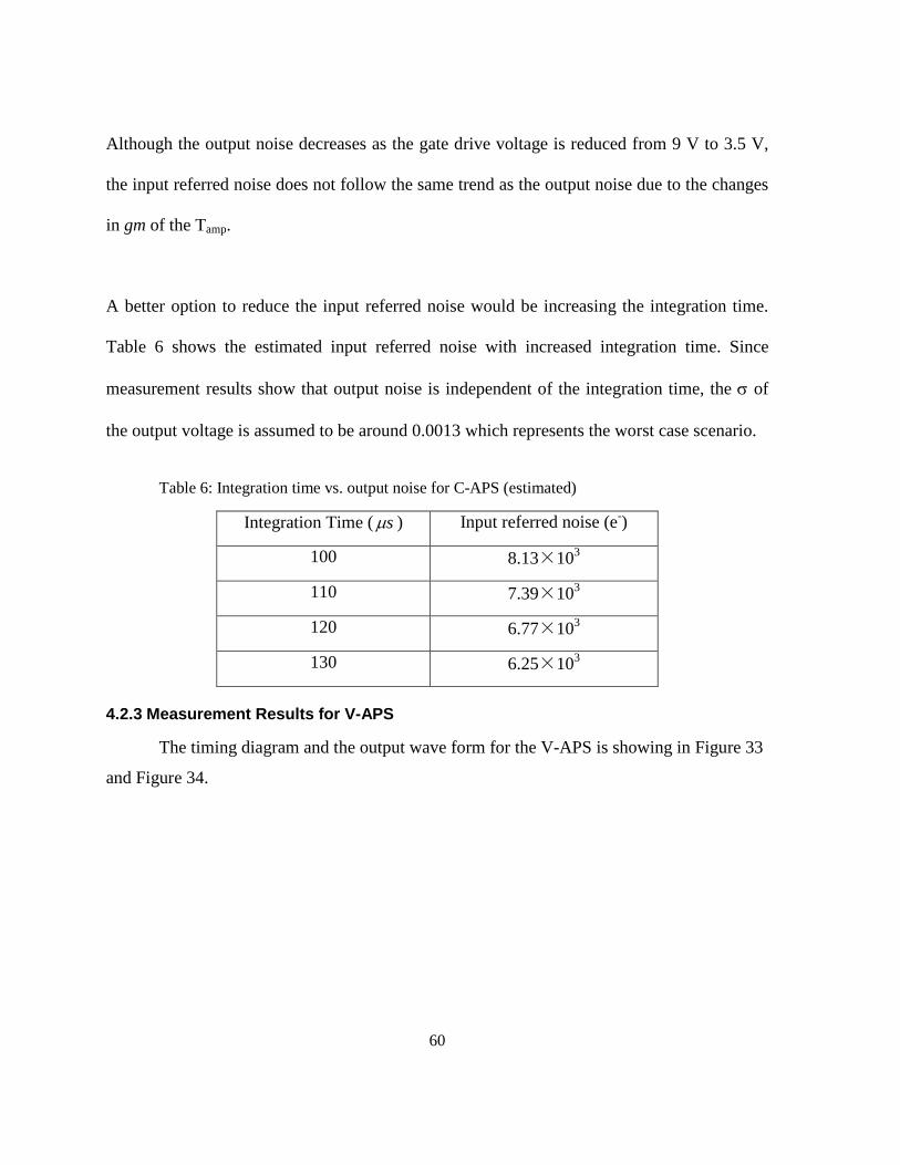
60
Although the output noise decreases as the gate drive voltage is reduced from 9 V to 3.5 V,
the input referred noise does not follow the same trend as the output noise due to the changes
in gm of the Tamp.
A better option to reduce the input referred noise would be increasing the integration time.
Table 6 shows the estimated input referred noise with increased integration time. Since
measurement results show that output noise is independent of the integration time, the σ of
the output voltage is assumed to be around 0.0013 which represents the worst case scenario.
Table 6: Integration time vs. output noise for C-APS (estimated)
Integration Time ( sµ ) Input referred noise (e-)
100 8.13×10³
110 7.39×10³
120 6.77×10³
130 6.25×10³
4.2.3 Measurement Results for V-APS
The timing diagram and the output wave form for the V-APS is showing in Figure 33
and Figure 34.
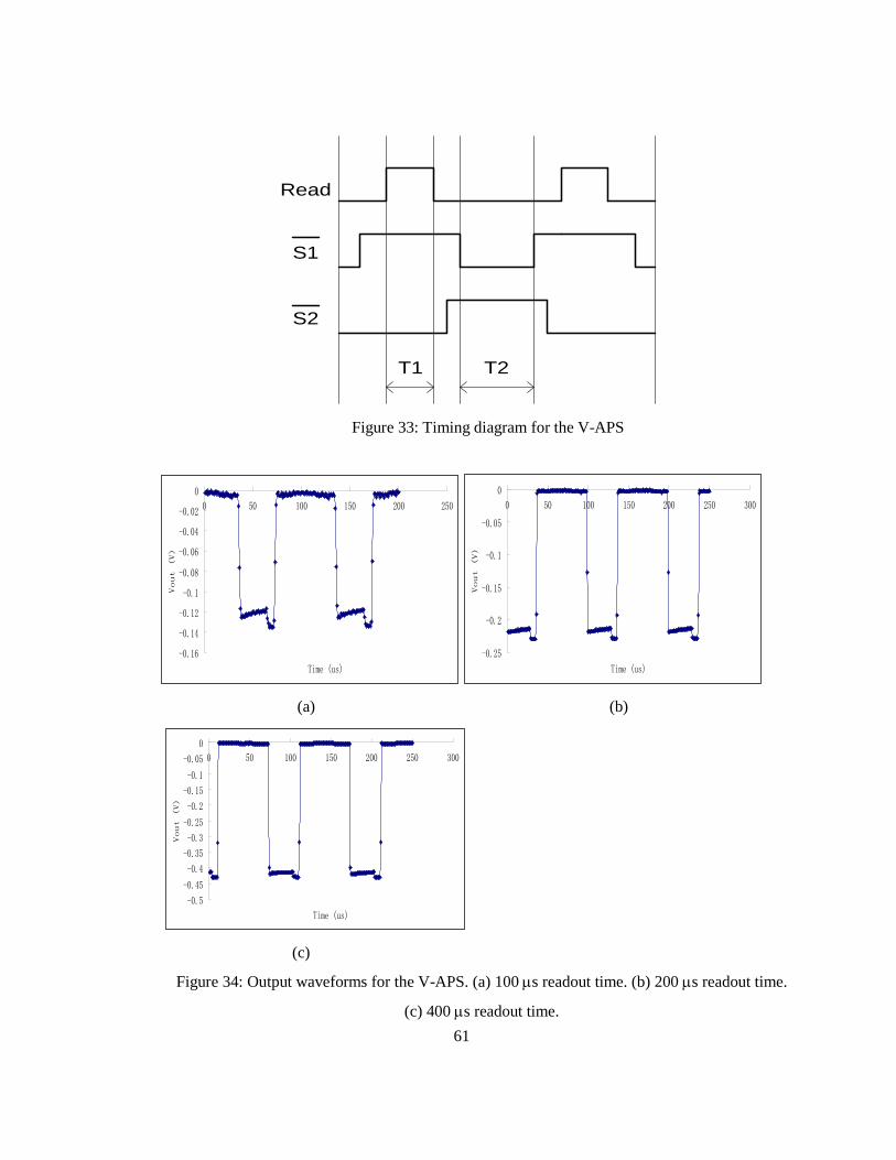
61
Read
S1
S2
T1 T2
Figure 33: Timing diagram for the V-APS
-0.16
-0.14
-0.12
-0.1
-0.08
-0.06
-0.04
-0.02
0
0 50 100 150 200 250
Time (us)
Vout (V)
-0.25
-0.2
-0.15
-0.1
-0.05
0
0 50 100 150 200 250 300
Time (us)
Vout (V)
(a) (b)
-0.5
-0.45
-0.4
-0.35
-0.3
-0.25
-0.2
-0.15
-0.1
-0.05
0
0 50 100 150 200 250 300
Time (us)
Vout (V)
(c)
Figure 34: Output waveforms for the V-APS. (a) 100 µs readout time. (b) 200 µs readout time.
(c) 400 µs readout time.
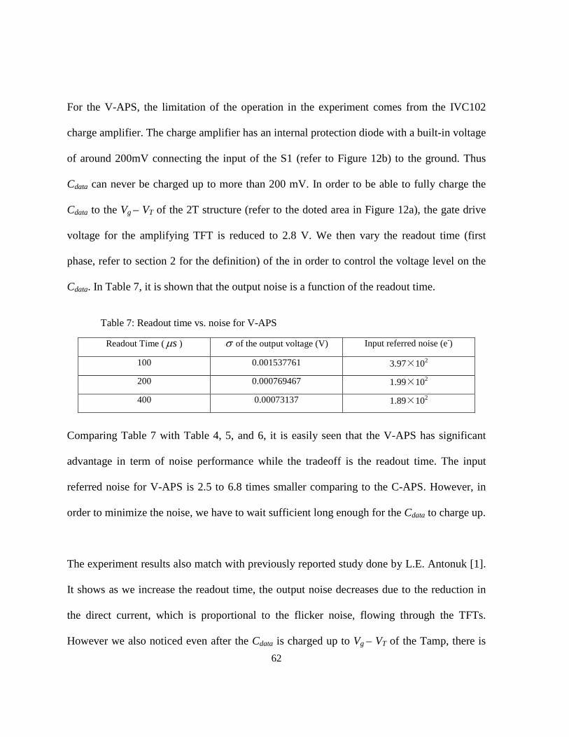
62
For the V-APS, the limitation of the operation in the experiment comes from the IVC102
charge amplifier. The charge amplifier has an internal protection diode with a built-in voltage
of around 200mV connecting the input of the S1 (refer to Figure 12b) to the ground. Thus
Cdata can never be charged up to more than 200 mV. In order to be able to fully charge the
Cdata to the Vg – VT of the 2T structure (refer to the doted area in Figure 12a), the gate drive
voltage for the amplifying TFT is reduced to 2.8 V. We then vary the readout time (first
phase, refer to section 2 for the definition) of the in order to control the voltage level on the
Cdata. In Table 7, it is shown that the output noise is a function of the readout time.
Table 7: Readout time vs. noise for V-APS
Readout Time ( sµ ) σ of the output voltage (V) Input referred noise (e-)
100 0.001537761 3.97×10²
200 0.000769467 1.99×10²
400 0.00073137 1.89×10²
Comparing Table 7 with Table 4, 5, and 6, it is easily seen that the V-APS has significant
advantage in term of noise performance while the tradeoff is the readout time. The input
referred noise for V-APS is 2.5 to 6.8 times smaller comparing to the C-APS. However, in
order to minimize the noise, we have to wait sufficient long enough for the Cdata to charge up.
The experiment results also match with previously reported study done by L.E. Antonuk [1].
It shows as we increase the readout time, the output noise decreases due to the reduction in
the direct current, which is proportional to the flicker noise, flowing through the TFTs.
However we also noticed even after the Cdata is charged up to Vg – VT of the Tamp, there is

63
still significant amount of direct current going through the TFTs. To further investigate this
problem, the 2T structure is tested using the semiconductor parameter analyzer and the result
is shown in Figure 35.
0
100
200
300
400
500
600
700
800
0 2 4 6 8 10
Vg (V)
Id (
nA
)
0
100
200
300
400
500
600
700
800
0 2 4 6 8 10
Vs (V)
Id (
nA)
(a) (b)
Figure 35: (a) Id vs. Vg (b) Id vs. Vs
Figure 35(a) shows the Id vs. Vg curve with 9V at the drain of Tamp and 9V at the gate of Tread.
VT of the structure can be extrapolated to be around 2.5 V. In, Figure 35(b), the gate of Tamp,
the drain of Tamp, and the gate of Tread is kept at the 9 V and the source of Tread is swept from
0 V to 9 V. It is shown that even when the voltage at the source of Tread reaches 7.5V, which
is around Vg – VT of the 2T structure, there is still around 2 nA of current flowing through the
transistors. This phenomenon can be explained by comparing the Id vs Vg curve of the a-Si
TFT to that of the crystalline silicon transistor shown in Figure 36. It is shown that for
crystalline silicon transistor, the ON-OFF ratio of the current is much higher and VT can be
defined. On the other hand, for a-Si TFT, aside from the high OFF or leakage current, it is
also very hard to define the VT, due to the fact that the corner on the IV curve for a-Si TFT is
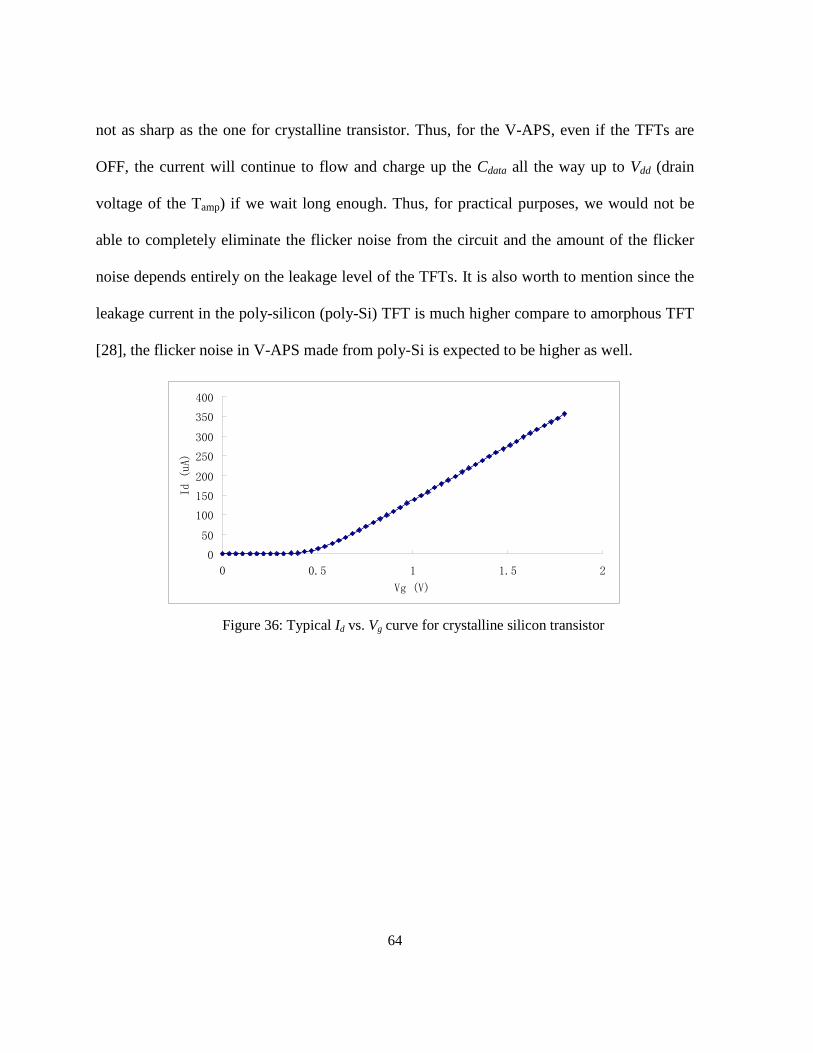
64
not as sharp as the one for crystalline transistor. Thus, for the V-APS, even if the TFTs are
OFF, the current will continue to flow and charge up the Cdata all the way up to Vdd (drain
voltage of the Tamp) if we wait long enough. Thus, for practical purposes, we would not be
able to completely eliminate the flicker noise from the circuit and the amount of the flicker
noise depends entirely on the leakage level of the TFTs. It is also worth to mention since the
leakage current in the poly-silicon (poly-Si) TFT is much higher compare to amorphous TFT
[28], the flicker noise in V-APS made from poly-Si is expected to be higher as well.
0
50
100
150
200
250
300
350
400
0 0.5 1 1.5 2
Vg (V)
Id (
uA)
Figure 36: Typical Id vs. Vg curve for crystalline silicon transistor

65
Chapter 5 Conclusion
5.1 Summary
Both detailed analytical noise analysis and experimental noise measurements are
presented in this thesis. TFT leakage noise, circuit thermal noise, circuit flicker noise, data
line noise and the charge amplifier noise are considered. Both theoretical and experimental
results obtained in this study verified that V-APS is superior compared to the C-APS circuit
in term of the noise performance due to the lower flicker noise in the V-APS circuit.
Experiment results show that the input referred noise of V-APS is significantly smaller
comparing to C-APS. It is also concluded that the noise level in V-APS is independent of the
bias voltage of the circuitry.
Although reduced in V-APS, the flicker noise is still presented and could not be easily
eliminated due to the high leakage current presented in a-Si TFTs and even worse, in poly-Si
TFTs. The tradeoff for low noise in V-APS is the long readout time, which makes it
unpractical for real time imaging system.
5.2 Projected Results
In this section, the best case noise performance and signal to noise ration (SNR) are
compared for both C-APS and V-APS made with a-Si and poly-Si technology. The
parameters used for the calculation are listed in table 8.

66
Table 8: Parameters for best case noise calculation
TFT Parameters a-Si poly-Si
Tamp width (µm) 400 400
Tamp length (µm) 20 20
Tread width (µm) 200 200
Tread length (µm) 20 20
Treset width (µm) 200 200
Treset length (µm) 20 20
Effective channel mobility (cm2/Vs) 0.5 150
Threshold voltage (V) 2.5 1
Effective pixel capacitor (pF) 1 1
The data line capacitance (Cdata) and feedback capacitance (Cf) are assumed to be 60 pf and
1 pf, respectively. For more comprehensive results, the reset TFT leakage current shot noise
and reset noise (kTC) noise are included in this section. The leakage current noise associated
with the reset TFT is given by
qTITFT
TFT =σ (77)

67
where ITFT is the TFT leakage current, T is the frame time which equals to 33 ms, and q is
the electron charge. For the calculation, we assumed a leakage current of 0.03 fA per micron
of gate width for the a-Si, and a leakage current of 1.5 fA per micron of gate width for the
poly-Si [25]. Reset noise can be calculated by
effreset C
kT=σ (78)
where Ceff is the effective detector node capacitance.
Performing the same analysis, which has been done in section 3 with the new parameters, the
new results are shown in the table 9.
Table 9: Leakage current noise and reset noise
a-Si poly-Si
Reset TFT leakage current noise (electrons) 18 125
Reset (kTC) noise (electrons) 284 284
The total noise for both a-Si and poly-Si are calculated and shown in table 10.
Table 10: Total input referred noise
Input referred noise (electrons) a-Si poly-Si
C-APS 527 348
V-APS 286 312
For the real time fluoroscopy application where the inputs signal level is about 1000
electrons. The SNR is calculated and listed in table 11.

68
Table 11: Total input referred noise
SNR (absolute) a-Si poly-Si
C-APS 1.9 2.9
V-APS 3.5 3.2
Other than better noise performance comparing to a-Si, poly-Si also has speed advantage due
to its higher electron mobility (100 times of the electron mobility in a-Si). Poly-Si also has
high hole mobility so complementary designs can also be achieved with poly-Si. (where it is
impossible with a-Si).
5.3 Potential Future Research
Some future work can be done to improve the measurement results obtained in this
study in terms of accuracy and completeness. First of all, to get more accurate results for both
C-APS and V-APS, better model of NI card with more sophisticated ADC (16bit or higher)
should be used. This allows us to have higher output voltage level with the same degree of
accuracy when taking noise measurement. Next, to make gain of the circuits higher, discrete
feedback capacitor should be used instead of the default ones attached to the IVC102 charge
amplifier used in this work. The discrete feedback capacitor should have smaller value
compare to the default ones in order to have a lower input referred noise figure. For the V-
APS noise measurement, it is necessary to find or design a charge amplifier that does not
have such a low input voltage limitation as in the case of IVC102. For more ambitious
measurement in the future, double sampling mechanism can be included. This would further
reduce the flicker noise figures measured in this study.

69
References
[1]. L.E. Antonuk, M. Koniczek, J. McDonald, Y. El-Mohri, Q. Zhao, and M. Behravan, “Noise Characterization of Polycrystalline Silicon Thin Film Transistors for X-ray Imagers Based on Active Pixel Architectures”, Mater. Res. Soc. Symp. Proc. Vol. 1066, 2008
[2]. Karim S. Karim, “Pixel Architectures for Digital Imaging Using Amorphous Silicon Technology”, PhD thesis, University of Waterloo, 2002
[3]. Farhad Taghibakhsh, “Active Pixel Sensor Architectures for High Resolution Large Area Digital Imaging”, PhD thesis, University of Waterloo, 2008
[4]. S. O. Kasap, “Crystalline and Amorphous Silicon”, Principles of Electronic Materials and Devices, 2005
[5]. Michael Shur, Michael Hack, and John G. Shaw, “A new analytic model for amorphous silicon thin-film transistors”, J.Appl.Phys., Vol.66, No.7, 1 October 1989.
[6]. Cherie R. Kagan and Paul Andry, “Hydrogenated Amorphous Silicon Thin-Film Transistors”, Thin-Film Transistor, Chapter 3.2, 2003
[7]. C. van Berkel, M.J. Powell, “The resolution of amorphous silicon thin film transistor instability mechanisms using ambipolar transistors,” Applied Physics Letters, 51, p. 1094,1987.
[8]. M.J. Powell, C. van Berkel, A.R. Franklin, S.C. Deane, W.I. Milne, “Defect Pool Model
in Amorphous Silicon Thin-Film Transistors,” Physical Review B, 45, pp. 4160-4170, 1992.
[9]. W.B. Jackson, M.D. Moyer, “Creation of near interface defects in hydrogenated
amorphous silicon-silicon nitride heterojunctions: The role of hydrogen,” Physical Review B, 36, p. 6217, 1987.
[10]. C. Chiang, J. Kanicki, K. Takechi, “Electrical Instability of Hydrogenated
Amorphous Silicon Thin-Film Transistors for Active-Matrix Liquid-Crystal Displays,” Japan Journal of Applied Physics, 37(1), Part A, p. 4704-10, 1998
70
[11]. R. Oritsuki, T. Horii, A. Sasano, K. Tsutsui, T. Koizumi, Y. Kaneko, and T. Tsukada, “Threshold Voltage Shift of Amorphous Silicon Thin-Film Transistors During Pulse Operation,” Jpn. J. Appl. Phys., 30, Part 1, No. 12B, pp. 3719-3723, 1991.
[12]. C. Huang, T. Teng, J. Tsai and H. Cheng, “The Instability Mechanisms of
Hydrogenated Amorphous Silicon Thin Film Transistors under AC Bias Stress,” Jpn. J. Appl. Phys., 39, Part 1, No. 7A, pp. 3867-3871, July 2000
[13]. Cherie R. Kagan, Paul Andry, “Thin Film Transistors”, Marcel Dekker, Inc, New
York, 2003 [14]. Y. Kuo, Editor of textbook “Amorphous Silicon Thin Film Transistors,” Kluwer
Academic Publishers, Norwell, MA, 2003 [15]. L. Hojin, L. Yen-Chung, H.-P.D. Shieh, J. Kanicki, “Current-Scaling a-Si:H TFT
Pixel-Electrode Circuit for AM-OLEDs: Electrical Properties and Stability” IEEE Transactions on Electron Devices, vol. 54, no. 9, pp. 2403-2410, September 2007.
[16]. Z. Huang, T. Ando, “A Novel Amplified Image Sensor with a-Si Photoconductor and
MOS Transistors,” IEEE Transactions on Electron Devices, 37(6), pp. 1432-1438, June 1990.
[17]. Golnaz Sanaie-Fard, “Low Noise High Dynamic Range Pixel Architecture in
Amorphous Silicon Technology for Diagnostic Medical Imaging Applications,” MASc Thesis , Simon Fraser University, 2002.
[18]. G. Sanaie, R. Sanaie, K. S. Karim, “Diagnostic X-ray Imaging Using Amorphous
Silicon Technology,” 106th Meeting of the Electrochemical Society, Hawaii, USA, October 2004.
[19]. J.M. Boudry and L.E. Antonuk, “Current-noise-power spectra of amorphous silicon
thin-film transistors,” Journal of Applied Physics, 76, pp.2529-2534, 1994. [20]. K.S. Karim, A. Nathan, J.A. Rowlands, “Feasibility of current mediated amorphous
silicon active pixel sensor readout circuits for large area diagnostic medical imaging,” in Opto-Canada: SPIE Regional Meeting on Optoelectronics, Photonics and Imaging, SPIE TD01, pp. 358-360, May 2002.
[21]. Paul R. Gray, Paul J. Hurst, Stephen H. Lewis, and Robert G. Meyer, “Analysis and
Design of Analog Integrated Circuits”, John Wiley & Sons, 2001. [22]. A.L. McWhorter, “1/f noise and germanium surface properties,” Semiconductor
Surface Physics, University of Pennsylvania Press, Philadelphia, pp. 207-228, 1956.
71
[23]. F.N. Hooge, A. Hoppenbrouwers, “Amplitude Distribution of 1/f noise,” Physica, 42, pp.331-339, 1969.
[24]. F.N. Hooge, L.K.J. Vandamme, “Lattice scattering causes 1/f noise,” Phys. Lett., 66A,
pp.316-326, 1978. [25]. M.H. Izadi, , K.S. Karim, A. Nathan, J.A. Rowlands, “Low-noise pixel architecture
for advanced diagnostic medical x-ray imaging applications”, Proc. SPIE, 6142, 2006. [26]. J. Rhayem, D. Rigaud, M. Valenza, N. Szydlo, and H. Lebrun, “1/f noise
investigations in long channel length amorphous silicon thin-film transistors,” J. Appl. Phys., 87(4), 1983–1989, 2000.
[27]. D. Rigaud , M. Valenza , J. Rhayem, “Low frequency noise in thin film transistors”,
IEE Proc. Circuits Devices Syst., 149(1), 75-82, 2002. [28]. J.B. Boyce, J.P. Lu, J. Ho, R.A. Street, K. van Schuylenbergh, and Y. Wang, “Pulsed
Laser Crystallization of Amorphous Silicon for Polysilicon Flat Panel Imagers”, Journal of Non-Crystalline Solids 299-302, 731-735, 2002.

Related Documents