NJW4750T1 - 1 - Ver.0.4 http://www.njr.com/ Please note that this device is still under the development and therefore the specifications are subject to change. Quad Channel Combination Regulator FEATURES AEC-Q100 Qualified * Operating temperature range -40~125 C Including four regulators; Ch.1: Wide input range 1.2A buck converter. Ch.2: Low voltage 0.6A synchronous buck converter. Ch.3: Selectable regulator. w voltage 0.6A synchronous buck converter / Low voltage 0.3A LDO Ch.4: Low voltage 0.3A LDO e.g. ) Ta=85 C, fosc=2Mhz DC-DC Ch.1: 12V 3.3V/1000mA( (Included supply for Ch.2, 3, 4) Ch.2: 3.3V 1.8V/500mA Ch.3: 3.3V 1.2V/500mA LDO Ch.4: 3.3V 2.8V/200mA Wide operating input voltage range 3.9V(UVLO ON: 3.35V) to 40V (Ch.1) 2.4V to 5.5V (Ch.2, Ch.3, Ch.4) Free power-on sequence - Individual Power-Good Function ( High precision -7%, + 15%) - Individual Standby Function Protection function - UVLO (Under Voltage Lockout) - Over current protection function for more safety operation (Hiccup or Latch) - Thermal shutdown Oscillating frequency 280kHz to 2.4MHz External clock synchronization Anti-phase operation between Ch.1 and Ch.2 / 3 Current mode control buck converters Built-in compensation cicuit Soft start function *Reliability test is in progress now. APPLICATION GENERAL DESCRIPTION The NJW4750 is quad channel combination regulator including one wide input range buck converter and three secondary synchronous buck converter / LDO. Ch.3 can be selectable to the synchronous buck con- verter mode or LDO mode. Therefore, the NJW4750 expands the choices when building power supply block suitable for various applications. The switching regulators are operated anti-phase opera- tion between Ch.1 and Ch.2 / 3 in order to reduce EMI noise. Every regulator has individual enable pin and pow- er-good pin. Therefore, flexible power-on sequence configuration is available. The NJW4750 has two types of over-current protection according to application demand. Furthermore, it adopts a new overcurrent protection sequence which is more safety and contributes to min- iaturization of the inductor. Small package: 2.6mm × 3.4mm QFN is adopted suit- able for small application such as camera module. TARGET APPLICATION Camera Module(Automotive) Rader(Automotive) Photoelectric sensor(FA) Small Application and other. PACKAGE EQFN26 3.4mm x 2.6mm

Welcome message from author
This document is posted to help you gain knowledge. Please leave a comment to let me know what you think about it! Share it to your friends and learn new things together.
Transcript

NJW4750T1
- 1 - Ver.0.4
http://www.njr.com/ Please note that this device is still under the development and therefore the specifications are subject to change.
Quad Channel Combination Regulator FEATURES
AEC-Q100 Qualified *
Operating temperature range -40~125C
Including four regulators;
Ch.1: Wide input range 1.2A buck converter.
Ch.2: Low voltage 0.6A synchronous buck converter.
Ch.3: Selectable regulator.
w voltage 0.6A synchronous buck converter
/ Low voltage 0.3A LDO
Ch.4: Low voltage 0.3A LDO
e.g.) Ta=85 C, fosc=2Mhz
DC-DC Ch.1: 12V 3.3V/1000mA(
(Included supply for Ch.2, 3, 4)
Ch.2: 3.3V 1.8V/500mA
Ch.3: 3.3V 1.2V/500mA
LDO Ch.4: 3.3V 2.8V/200mA
Wide operating input voltage range
3.9V(UVLO ON: 3.35V) to 40V (Ch.1)
2.4V to 5.5V (Ch.2, Ch.3, Ch.4)
Free power-on sequence
- Individual Power-Good Function
(High precision -7%, + 15%)
- Individual Standby Function
Protection function
- UVLO (Under Voltage Lockout)
- Over current protection function for more safety operation
(Hiccup or Latch)
- Thermal shutdown
Oscillating frequency 280kHz to 2.4MHz
External clock synchronization
Anti-phase operation between Ch.1 and Ch.2 / 3
Current mode control buck converters
Built-in compensation cicuit
Soft start function
*Reliability test is in progress now.
APPLICATION
GENERAL DESCRIPTION
The NJW4750 is quad channel combination regulator
including one wide input range buck converter and
three secondary synchronous buck converter / LDO.
Ch.3 can be selectable to the synchronous buck con-
verter mode or LDO mode. Therefore, the NJW4750
expands the choices when building power supply block
suitable for various applications.
The switching regulators are operated anti-phase opera-
tion between Ch.1 and Ch.2 / 3 in order to reduce EMI
noise.
Every regulator has individual enable pin and pow-
er-good pin. Therefore, flexible power-on sequence
configuration is available.
The NJW4750 has two types of over-current protection
according to application demand.
Furthermore, it adopts a new overcurrent protection
sequence which is more safety and contributes to min-
iaturization of the inductor.
Small package: 2.6mm × 3.4mm QFN is adopted suit-
able for small application such as camera module.
TARGET APPLICATION
Camera Module(Automotive)
Rader(Automotive)
Photoelectric sensor(FA)
Small Application and other.
PACKAGE
EQFN26
GND
FB
V+
CFBR2
COUT
L
SBDNJW4133
VIN
CIN
R1
VOUT
SW
EN/SYNC
EN/SYNCHigh: ONLow: OFF
(Standby)
RT
RT
CC1
RC
COMP
CC2OVP
R4
R3GND
FB
V+
CFBR2
COUT
L
SBDNJW4133
VIN
CIN
R1
VOUT
SW
EN/SYNC
EN/SYNCHigh: ONLow: OFF
(Standby)
RT
RT
CC1
RC
COMP
CC2OVP
R4
R3
3.4mm x 2.6mm
NJW4750T1
- 2 - Ver.0.4
http://www.njr.com/ Please note that this device is still under the development and therefore the specifications are subject to change.
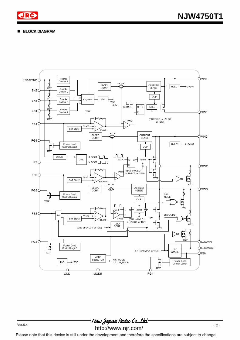
BLOCK DIAGRAM
NJW4750T1
- 3 - Ver.0.4
http://www.njr.com/ Please note that this device is still under the development and therefore the specifications are subject to change.
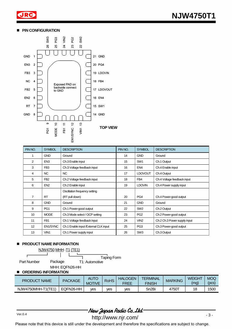
PIN CONFIGURATION
PIN NO. SYMBOL DESCRIPTION PIN NO. SYMBOL DESCRIPTION
1 GND Ground 14 GND Ground
2 EN3 Ch.3 Enable input 15 SW1 Ch.1 Output
3 FB3 Ch.3 Voltage feedback input 16 EN4 Ch.4 Enable input
4 NC NC 17 LDOVOUT Ch.4 Output
5 FB2 Ch.2 Voltage feedback input 18 FB4 Ch.4 Voltage feedback input
6 EN2 Ch.2 Enable input 19 LDOVIN Ch.4 Power supply input
7 RT
Oscillation frequency setting
(RT pull down) 20 PG4 Ch.4 Power-good output
8 GND Ground 21 GND Ground
9 PG1 Ch.1 Power-good output 22 SW2 Ch.2 Output
10 MODE Ch.3 Mode select / OCP setting 23 PG2 Ch.2 Power-good output
11 FB1 Ch.1 Voltage feedback input 24 VIN2 Ch.2 Ch.3 Power supply input
12 EN1/SYNC Ch.1 Enable input /External CLK input 25 PG3 Ch.3 Power-good output
13 VIN1 Ch.1 Power supply input 26 SW3 Ch.3 Output
PRODUCT NAME INFORMATION
ORDERING INFORMATION
PRODUCT NAME PACKAGE AUTO
MOTIVE RoHS
HALOGEN
FREE
TERMINAL
FINISH MARKING
WEIGHT (mg)
MOQ (pcs)
NJW4750MHH-T1(TE1) EQFN26-HH yes yes yes Sn2Bi 4750T 18 1500
NJW4750 MHH -T1 (TE1)
Part Number Package
MHH: EQFN26-HH
Taping Form
TOP VIEW
T1: Automotive

NJW4750T1
- 4 - Ver.0.4
http://www.njr.com/ Please note that this device is still under the development and therefore the specifications are subject to change.
ABSOLUTE MAXIMUM RATINGS
PARAMETER SYMBOL MAXIMUM RATING UNIT
Supply Voltage VVIN1 -0.3 to +45 V
VVIN2, VLDOVIN -0.3 to +7 V
Voltage between terminals
VIN1 - SW1 VVIN1–SW1 +45 V
Voltage between terminals
VIN2 - SW2/SW3
VVIN2–SW2
VVIN2–SW3 +7 V
EN/SYNC pin Voltage VEN1/SYNC -0.3 to +45 V
EN pin Voltage VEN2, VEN3 -0.3 to +7 V
VEN4 -0.3 to +45 V
FB pin Voltage VFB1, VFB2, VFB3, VFB4 -0.3 to +7 V
PG pin Voltage VPG1, VPG2, VPG3, VPG4 -0.3 to +7 V
Power Dissipation(Ta=25C) PD EQFN26-HH 850 (1)
2500 (2) mW
Junction Temperature Range Tj -40 to +150 C
Operating Temperature Range Topr -40 to +125 C
Storage Temperature Range Tstg -50 to +150 C
(1): Mounted on glass epoxy board. (101.5×114.5×1.6mm:based on EIA/JEDEC standard,2layers, with Exposed Pad) (2): Mounted on glass epoxy board. (101.5×114.5×1.6mm:based on EIA/JEDEC standard,4layers, with Exposed Pad) (For 4Layers: Applying 99.5×99.5mm inner Cu area and a thermal via hall to a board based on JEDEC standard JESD51-5)
RECOMMENDED OPERATING CONDITIONS
PARAMETER SYMBOL VALUE UNIT
Supply Voltage VVIN1 3.9 to 40 V
VVIN2, VLDOVIN 2.4 to 5.5 V
EN/SYNC pin Voltage VEN1/SYNC 0 to 40 V
EN pin Voltage VEN2, VEN3, VEN4 0 to 5.5 V
PG pin Voltage VPG1, VPG2, VPG3, VPG4 0 to 5.5 V
Timing Resistor RT 1.8 to 27 k
Oscillating Frequency fOSC 250 to 2600 kHz
External Clock fSYNC fOSC0.9 to fOSC1.7
Upper limit 2800kHz kHz
NJW4750T1
- 5 - Ver.0.4
http://www.njr.com/ Please note that this device is still under the development and therefore the specifications are subject to change.
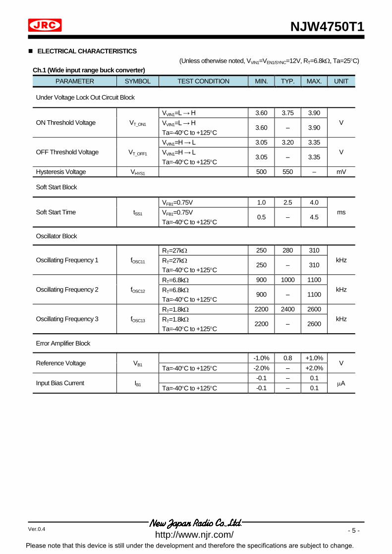
ELECTRICAL CHARACTERISTICS
(Unless otherwise noted, VVIN1=VEN1/SYNC=12V, RT=6.8k, Ta=25C)
Ch.1 (Wide input range buck converter)
PARAMETER SYMBOL TEST CONDITION MIN. TYP. MAX. UNIT
Under Voltage Lock Out Circuit Block
ON Threshold Voltage VT_ON1
VVIN1=L → H 3.60 3.75 3.90
V VVIN1=L → H
Ta=-40C to +125C 3.60 – 3.90
OFF Threshold Voltage VT_OFF1
VVIN1=H → L 3.05 3.20 3.35
V VVIN1=H → L
Ta=-40C to +125C 3.05 – 3.35
Hysteresis Voltage VHYS1 500 550 – mV
Soft Start Block
Soft Start Time tSS1
VFB1=0.75V 1.0 2.5 4.0
ms VFB1=0.75V
Ta=-40C to +125C 0.5 – 4.5
Oscillator Block
Oscillating Frequency 1 fOSC11
RT=27k 250 280 310
kHz RT=27k
Ta=-40C to +125C 250 – 310
Oscillating Frequency 2 fOSC12
RT=6.8k 900 1000 1100
kHz RT=6.8k
Ta=-40C to +125C 900 – 1100
Oscillating Frequency 3 fOSC13
RT=1.8k 2200 2400 2600
kHz RT=1.8k
Ta=-40C to +125C 2200 – 2600
Error Amplifier Block
Reference Voltage VB1 -1.0% 0.8 +1.0%
V Ta=-40C to +125C -2.0% – +2.0%
Input Bias Current IB1 -0.1 – 0.1
A Ta=-40C to +125C -0.1 – 0.1

NJW4750T1
- 6 - Ver.0.4
http://www.njr.com/ Please note that this device is still under the development and therefore the specifications are subject to change.
ELECTRICAL CHARACTERISTICS
(Unless otherwise noted, VVIN1=VEN1/SYNC=12V, RT=6.8k, Ta=25C)
Ch.1 (Wide input range buck converter)
PARAMETER SYMBOL TEST CONDITION MIN. TYP. MAX. UNIT
PWM Comparator Block
Maximum Duty Cycle MAXDUTY1
VFB1=0.7V 100 – –
% VFB1=0.7V
Ta=-40C to +125C 100 – –
Minimum OFF Time tOFF1-min – 60 – ns
Minimum ON Time tON1-min – 55 – ns
Over Current Protection Circuit Block
Cool Down Time tCOOL1 RMODE=36k or 10 k – 75 – ms
Output Block
Output ON Resistance RON1 ISW1=0.8A – 0.5 0.8
Switching Current Limit ILIM1 1.4 1.7 2.0 A
Switching Leak Current ILEAK1
VEN1/SYNC=0V, VVIN1=40V
VSW1=0V
Ta=-40C to +125C
– – 4 A
Enable Control / Sync Block (EN1/SYNC)
High Threshold Voltage VTHH_EN1/SYNC
VEN1/SYNC=L → H 1.6 – 40.0
V VEN1/SYNC=L → H
Ta=-40C to +125C 1.6 – 40.0
Low Threshold Voltage VTHL_EN1/SYNC
VEN1/SYNC=H → L 0 – 0.4
V VEN1/SYNC=H → L
Ta=-40C to +125C 0 – 0.4
Input Bias Current IEN1/SYNC
VEN1/SYNC=5V – 1 3
A VEN1/SYNC=5V
Ta=-40C to +125C – – 5

NJW4750T1
- 7 - Ver.0.4
http://www.njr.com/ Please note that this device is still under the development and therefore the specifications are subject to change.
ELECTRICAL CHARACTERISTICS
(Unless otherwise noted, VVIN1=VEN1/SYNC=12V, RT=6.8k, Ta=25C)
Ch.1 (Wide input range buck converter)
PARAMETER SYMBOL TEST CONDITION MIN. TYP. MAX. UNIT
Power Good Block(PG1)
High Level Detection
Reference Voltage VTHH_PG1
Rising 0.836 – 0.924 V
Rising, Ta=-40C to +125C 0.836 – 0.924
Low Level Detection
Reference Voltage VTHL_PG1
Rising 0.745 – 0.775 V
Rising, Ta=-40C to +125C 0.745 – 0.775
Hysteresis Voltage VHYS_PG1 – 16 – mV
Power Good ON Resistance RON_PG1 IPG1=10mA – 100 –
Leak Current at OFF State ILEAK_PG1
VPG1=5.5V – – 0.1
A VPG1=5.5V
Ta=-40C to +125C – – 0.1

NJW4750T1
- 8 - Ver.0.4
http://www.njr.com/ Please note that this device is still under the development and therefore the specifications are subject to change.
ELECTRICAL CHARACTERISTICS
(Unless otherwise noted, VVIN1=12V, VVIN2=VEN2=3.3V, RT=6.8k, Ta=25C)
Ch.2 (Low voltage synchronous buck converter)
PARAMETER SYMBOL TEST CONDITION MIN. TYP. MAX. UNIT
Under Voltage Lock Out Circuit Block
ON Threshold Voltage VT_ON2
VVIN2=L → H 2.10 2.25 2.40
V VVIN2=L → H
Ta=-40C to +125C 2.10 – 2.40
OFF Threshold Voltage VT_OFF2
VVIN2=H → L 2.00 2.15 2.30
V VVIN2=H → L
Ta=-40C to +125C 2.00 – 2.30
Hysteresis Voltage VHYS2 50 100 – mV
Soft Start Block
Soft Start Time tSS2
V FB2=0.75V 1.0 2.5 4.0
ms V FB2=0.75V
Ta=-40C to +125C 0.5 – 4.5
Oscillator Block
Oscillating Frequency 1 fOSC21
RT=27k 250 280 310
kHz RT=27k
Ta=-40C to +125C 250 – 310
Oscillating Frequency 2 fOSC22
RT=6.8k 900 1000 1100
kHz RT=6.8k
Ta=-40C to +125C 900 – 1100
Oscillating Frequency 3 fOSC23
RT=1.8k 2200 2400 2600
kHz RT=1.8k
Ta=-40C to +125C 2200 – 2600
Error Amplifier Block
Reference Voltage VB2 -1.0% 0.8 +1.0%
V Ta=-40C to +125C -2.0% – +2.0%
Input Bias Current IB2 -0.1 – 0.1
A Ta=-40C to +125C -0.1 – 0.1

NJW4750T1
- 9 - Ver.0.4
http://www.njr.com/ Please note that this device is still under the development and therefore the specifications are subject to change.
ELECTRICAL CHARACTERISTICS
(Unless otherwise noted, VVIN1=12V, VVIN2=VEN2=3.3V, RT=6.8k, Ta=25C)
Ch.2 (Low voltage synchronous buck converter)
PARAMETER SYMBOL TEST CONDITION MIN. TYP. MAX. UNIT
PWM Comparator Block
Maximum Duty Cycle MAXDUTY2
VFB2=0.7V 100 – –
% VFB2=0.7V
Ta=-40C to +125C 100 – –
Minimum OFF Time tOFF2-min – 80 – ns
Minimum ON Time tON2-min – 55 – ns
Over Current Protection Circuit Block
Cool Down Time tCOOL2 RMODE=36k or 10 k – 75 – ms
Output Block
Pch Output ON Resistance RONP2 ISW2SOURCE=0.5A – 0.5 0.8
Nch Output OFF Resistance RONN2 ISW2SINK=0.5A – 0.3 0.5
Switching Current Limit ILIM2 0.7 1.0 1.3 A
Switching Leak Current ILEAK2
VEN2=0V, VVIN2=5.5V
VSW2=0V
Ta=-40C to +125C
– – 4 A
Enable Control Block (EN2)
High Threshold Voltage VTHH_EN2
VEN2=L → H 1.0 – 5.5
V VEN2=L → H
Ta=-40C to +125C 1.0 – 5.5
Low Threshold Voltage VTHL_EN2
VEN2=H → L 0 – 0.4
V VEN2=H → L
Ta=-40C to +125C 0 – 0.4
Input Bias Current IEN2
VEN2=3.3V – 7 14
A VEN2=3.3V
Ta=-40C to +125C – – 14

NJW4750T1
- 10 - Ver.0.4
http://www.njr.com/ Please note that this device is still under the development and therefore the specifications are subject to change.
ELECTRICAL CHARACTERISTICS
(Unless otherwise noted, VVIN1=12V, VVIN2=VEN2=3.3V, RT=6.8k, Ta=25C)
Ch.2 (Low voltage synchronous buck converter)
PARAMETER SYMBOL TEST CONDITION MIN. TYP. MAX. UNIT
Power-good block (PG2)
High Level Detection
Reference Voltage VTHH_PG2
Rising 0.836 – 0.924 V
Rising, Ta=-40C to +125C 0.836 – 0.924
Low Level Detection
Reference Voltage VTHL_PG2
Rising 0.745 – 0.775 V
Rising, Ta=-40C to +125C 0.745 – 0.775
Hysteresis Voltage VHYS_PG2 – 16 – mV
Power Good ON Resistance RON_PG2 IPG2=10mA – 100 –
Leak Current at OFF State ILEAK_PG2
VPG2=5.5V – – 0.1
A VPG2=5.5V
Ta=-40C to +125C – – 0.1

NJW4750T1
- 11 - Ver.0.4
http://www.njr.com/ Please note that this device is still under the development and therefore the specifications are subject to change.
ELECTRICAL CHARACTERISTICS
(Unless otherwise noted, VVIN1=12V, VVIN2=VEN3=3.3V, RT=6.8k , Ta=25C)
Ch.3 (Selectable Regulator: Common for SW Reg. MODE and LDO MODE)
PARAMETER SYMBOL TEST CONDITION MIN. TYP. MAX. UNIT
Enable Control Block(EN3)
High Threshold Voltage VTHH_EN3
VEN3=L → H 1.0 – 5.5
V VEN3=L → H
Ta=-40C to +125C 1.0 – 5.5
Low Threshold Voltage VTHL_EN3
VEN3=H → L 0 – 0.4
V VEN3=H → L
Ta=-40C to +125C 0 – 0.4
Input Bias Current IEN3
VEN3=3.3V – 7 14
A VEN3=3.3V
Ta=-40C to +125C – – 14
Power Good Block (PG3)
High Level Detection
Reference Voltage VTHH_PG3
Rising 0.836 – 0.924 V
Rising, Ta=-40C to +125C 0.836 – 0.924
Low Level Detection
Reference Voltage VTHL_PG3
Rising 0.745 – 0.775 V
Rising, Ta=-40C to +125C 0.745 – 0.775
Hysteresis Voltage VHYS_PG3 – 16 – mV
Power Good ON Resistance RON_PG3 IPG3=10mA – 100 –
Leak Current at OFF State ILEAK_PG3
VPG3=5.5V – – 0.1
A VPG3=5.5V
Ta=-40C to +125C – – 0.1

NJW4750T1
- 12 - Ver.0.4
http://www.njr.com/ Please note that this device is still under the development and therefore the specifications are subject to change.
ELECTRICAL CHARACTERISTICS
(Unless otherwise noted, VVIN1=12V, VVIN2=VEN3=3.3V, RT=6.8k, RMODE= 82kΩ or 36kΩ, Ta=25C)
Ch.3 (Selectable Regulator: SW Reg. mode)
PARAMETER SYMBOL TEST CONDITION MIN. TYP. MAX. UNIT
Under Voltage Lock Out Circuit Block
ON Threshold Voltage VT_ON3
VVIN2=L → H 2.10 2.25 2.40
V VVIN2=L → H
Ta=-40C to +125C 2.10 – 2.40
OFF Threshold Voltage VT_OFF3
VVIN2=H → L 2.00 2.15 2.30
V VVIN2=H → L
Ta=-40C to +125C 2.00 – 2.30
Hysteresis Voltage VHYS3 50 100 – mV
Soft Start Block
Soft Start Time tSS3
V FB3=0.75V 1.0 2.5 4.0
ms V FB3=0.75V
Ta=-40C to +125C 0.5 – 4.5
Oscillator Block
Oscillating Frequency 1 fOSC31
RT=27k 250 280 310
kHz RT=27k
Ta=-40C to +125C 250 – 310
Oscillating Frequency 2 fOSC32
RT=6.8k 900 1000 1100
kHz RT=6.8k
Ta=-40C to +125C 900 – 1100
Oscillating Frequency 3 fOSC33
RT=1.8k 2200 2400 2600
kHz RT=1.8k
Ta=-40C to +125C 2200 – 2600
Error Amplifier Block
Reference Voltage VB3 -1.0% 0.8 +1.0%
V Ta=-40C to +125C -2.0% – +2.0%
Input Bias Current IB3 -0.1 – 0.1
A Ta=-40C to +125C -0.1 – 0.1

NJW4750T1
- 13 - Ver.0.4
http://www.njr.com/ Please note that this device is still under the development and therefore the specifications are subject to change.
ELECTRICAL CHARACTERISTICS
(Unless otherwise noted, VVIN1=12V, VVIN2=VEN3=3.3V, RT=6.8k, RMODE= 82kΩ or 36kΩ, Ta=25C)
Ch.3 (Selectable Regulator: SW Reg. mode)
PARAMETER SYMBOL TEST CONDITION MIN. TYP. MAX. UNIT
PWM Comparator Block
Maximum Duty Cycle MAXDUTY3
VFB3=0.7V 100 – –
% VFB3=0.7V
Ta=-40C to +125C 100 – –
Minimum OFF Time tOFF3-min – 80 – ns
Minimum ON Time tON3-min – 55 – ns
Over Current Protection Circuit Block
COOL DOWN Time tCOOL3 RMODE=36k – 75 – ms
Output Block
Pch Output ON Resistance RONP3 ISW3SOURCE=0.5A – 0.5 0.8
Nch Output ON Resistance RONN3 ISW3SINK=0.5A – 0.3 0.5
Switching Current Limit ILIM3 0.7 1.0 1.3 A
Switching Leak Current ILEAK3
VEN3=0V, VVIN2=5.5V
VSW3=0V
Ta=-40C to +125C
– – 4 A

NJW4750T1
- 14 - Ver.0.4
http://www.njr.com/ Please note that this device is still under the development and therefore the specifications are subject to change.
ELECTRICAL CHARACTERISTICS
(Unless otherwise noted, VVIN1=12V, VVIN2 =VEN3=3.3V, RT=6.8k, RMODE= OPEN or 10kΩ, Ta=25C)
Ch.3 (Selectable Regulator: LDO mode)
PARAMETER SYMBOL TEST CONDITION MIN. TYP. MAX. UNIT
Error Amplifier Block
Reference Voltage VB3 -1.0% 0.8 +1.0%
V Ta=-40C to +125C -2.0% – +2.0%
Output Current IOUT3
VOUT3×0.9 300 600 –
mA VOUT3×0.9
Ta=-40C to +125C 300 – –
Load Regulation ⊿VOUT3
/IOUT3
IOUT3=1 to 200mA – 0.003 0.009
%/mA IOUT3=1 to 200mA
Ta=-40C to +125C – – 0.020
Ripple Rejection RR3 ein=50mVrms, f=1kHz
VOUT3=2.8V, IOUT3=150mA –
TBD
(43) – dB
Dropout Voltage ⊿VIO3
IOUT3=200mA – 0.2 0.3
V IOUT3=200mA
Ta=-40C to +125C – – 0.4
Average Temperature
Coefficient of Output
Voltage
⊿VOUT3
/Ta
IOUT3=150mA
Ta=-20C to +75C – ±50 – ppm/C

NJW4750T1
- 15 - Ver.0.4
http://www.njr.com/ Please note that this device is still under the development and therefore the specifications are subject to change.
ELECTRICAL CHARACTERISTICS
(Unless otherwise noted, VVIN1=12V, VLDOVIN=VEN4 =3.3V, RT=6.8k, Ta=25C)
CH4 (LDO)
PARAMETER SYMBOL TEST CONDITION MIN. TYP. MAX. UNIT
Error Amplifier Block
Reference Voltage VB4 -1.0% 0.8 +1.0%
V Ta=-40C to +125C -2.0% – +2.0%
Output Current IOUT4
VOUT4×0.9 300 600 –
mA VOUT4×0.9
Ta=-40C to +125C 300 – –
Load Regulation ⊿VOUT4
/IOUT4
IOUT4=1 to 200mA – 0.003 0.009
%/mA IOUT4=1 to 200mA
Ta=-40C to +125C – – 0.020
Ripple Rejection RR4 ein=50mVrms, f=1kHz
VOUT4=2.8V, IOUT4=150mA –
TBD
(43) – dB
Dropout Voltage ⊿VIO4
IOUT4=200mA – 0.2 0.3
V IOUT4=200mA
Ta=-40C to +125C – – 0.4
Average Temperature
Coefficient of Output
Voltage
⊿VOUT4
/Ta
IOUT4=150mA
Ta=-20C to +75C – ±50 – ppm/C
Enable Control Block (EN4)
High Threshold Voltage VTHH_EN4
VEN4=L → H 1.0 – 5.5
V VEN4=L → H
Ta=-40C to +125C 1.0 – 5.5
Low Threshold Voltage VTHL_EN4
VEN4=H → L 0 – 0.4
V VEN4=H → L
Ta=-40C to +125C 0 – 0.4
Input Bias Current IEN4
VEN4=3.3V – 7 14
A VEN4=3.3V
Ta=-40C to +125C – – 14
Power Good Block (PG4)
High Level Detection
Reference Voltage VTHH_PG4
Rising 0.836 – 0.924 V
Rising, Ta=-40C to +125C 0.836 – 0.924
Low Level Detection
Reference Voltage VTHL_PG4
Rising 0.745 – 0.775 V
Rising, Ta=-40C to +125C 0.745 – 0.775
Hysteresis Voltage VHYS_PG4 – 16 – mV
Power Good ON Resistance RON_PG4 IPG4=10mA – 100 –
Leak Current at OFF State ILEAK_PG4
VPG4=5.5V – – 0.1
A VPG4=5.5V
Ta=-40C to +125C – – 0.1

NJW4750T1
- 16 - Ver.0.4
http://www.njr.com/ Please note that this device is still under the development and therefore the specifications are subject to change.
ELECTRICAL CHARACTERISTICS
(Unless otherwise noted, VVIN1=VEN1/SYNC=12V, VVIN2=VLDOVIN=VEN2=VEN3=VEN4=3.3V, RT=6.8k, Ta=25C)
Common Parameter
PARAMETER SYMBOL TEST CONDITION MIN. TYP. MAX. UNIT
General characteristic
Quiescent Current 1
(VIN1) IDD1
RL=no load, VFB1=0.9V – 2.3 3.5
mA RL=no load, VFB1=0.9V
Ta=-40C to +125C – – 3.5
Quiescent Current 2
(VIN2) IDD2
RL=no load
VFB2=0.9V, VFB3=0.9V – 2 3
mA RL=no load
VFB2=0.9V, VFB3=0.9V
Ta=-40C to +125C
– – 3
Quiescent Current 3
(VINLDO) IDDLDO
RL=no load, VFB4=0.9V – 0.1 0.2
mA RL=no load, VFB4=0.9V
Ta=-40C to +125C – – 0.2
Standby Current 1
(VIN1) IDD_STB1
VEN1/SYNC=0V
VEN2=0V
VEN3=0V
VEN4=0V
– – 3
A VEN1/SYNC=0V
VEN2=0V
VEN3=0V
VEN4=0V
Ta=-40C to +125C
– – 6
Standby Current 2
(VIN2) IDD_STB2
VEN1/SYNC=0V
VEN2=0V
VEN3=0V
VEN4=0V
– – 2
A VEN1/SYNC=0V
VEN2=0V
VEN3=0V
VEN4=0V
Ta=-40C to +125C
– – 4
Standby Current 3
(VINLDO) IDD_STBLDO
VEN1/SYNC=0V
VEN2=0V
VEN3=0V
VEN4=0V
– – 15
A VEN1/SYNC=0V
VEN2=0V
VEN3=0V
VEN4=0V
Ta=-40C to +125C
– – 20
NJW4750T1
- 17 - Ver.0.4
http://www.njr.com/ Please note that this device is still under the development and therefore the specifications are subject to change.
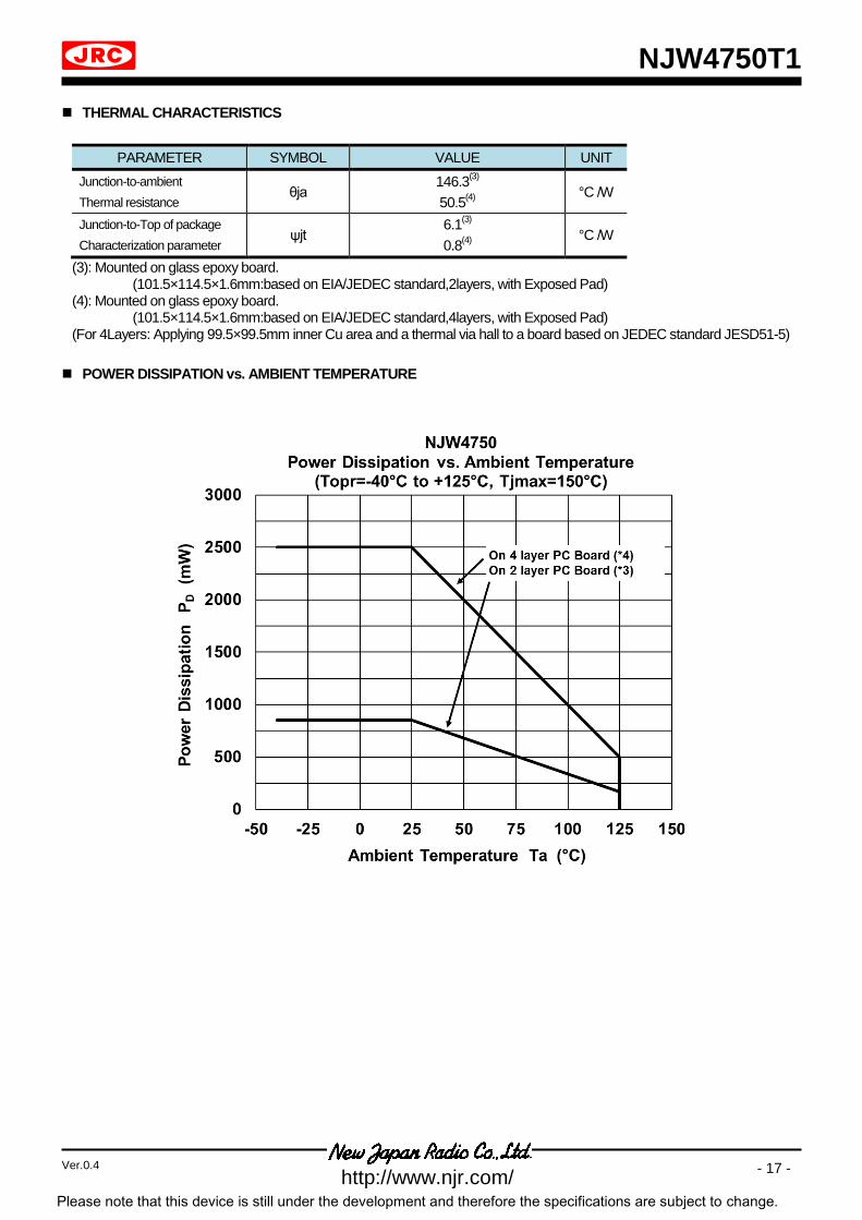
THERMAL CHARACTERISTICS
PARAMETER SYMBOL VALUE UNIT
Junction-to-ambient
Thermal resistance θja
146.3(3)
50.5(4)
°C /W
Junction-to-Top of package
Characterization parameter ψjt
6.1(3)
0.8(4)
°C /W
(3): Mounted on glass epoxy board. (101.5×114.5×1.6mm:based on EIA/JEDEC standard,2layers, with Exposed Pad) (4): Mounted on glass epoxy board. (101.5×114.5×1.6mm:based on EIA/JEDEC standard,4layers, with Exposed Pad) (For 4Layers: Applying 99.5×99.5mm inner Cu area and a thermal via hall to a board based on JEDEC standard JESD51-5)
POWER DISSIPATION vs. AMBIENT TEMPERATURE

NJW4750T1
- 18 - Ver.0.4
http://www.njr.com/ Please note that this device is still under the development and therefore the specifications are subject to change.
TYPICAL CHARACTERISTICS

NJW4750T1
- 19 - Ver.0.4
http://www.njr.com/ Please note that this device is still under the development and therefore the specifications are subject to change.
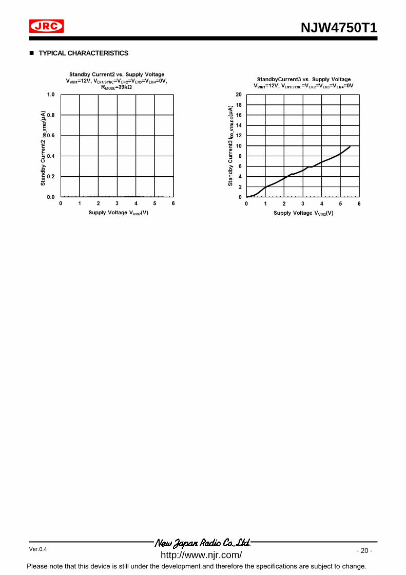
TYPICAL CHARACTERISTICS
NJW4750T1
- 20 - Ver.0.4
http://www.njr.com/ Please note that this device is still under the development and therefore the specifications are subject to change.
TYPICAL CHARACTERISTICS

NJW4750T1
- 21 - Ver.0.4
http://www.njr.com/ Please note that this device is still under the development and therefore the specifications are subject to change.
TYIPICAL CHARACTERISTICS

NJW4750T1
- 22 - Ver.0.4
http://www.njr.com/ Please note that this device is still under the development and therefore the specifications are subject to change.
TYPICAL CHARACTERISTICS

NJW4750T1
- 23 - Ver.0.4
http://www.njr.com/ Please note that this device is still under the development and therefore the specifications are subject to change.
TYPICAL CHARACTERITICS

NJW4750T1
- 24 - Ver.0.4
http://www.njr.com/ Please note that this device is still under the development and therefore the specifications are subject to change.
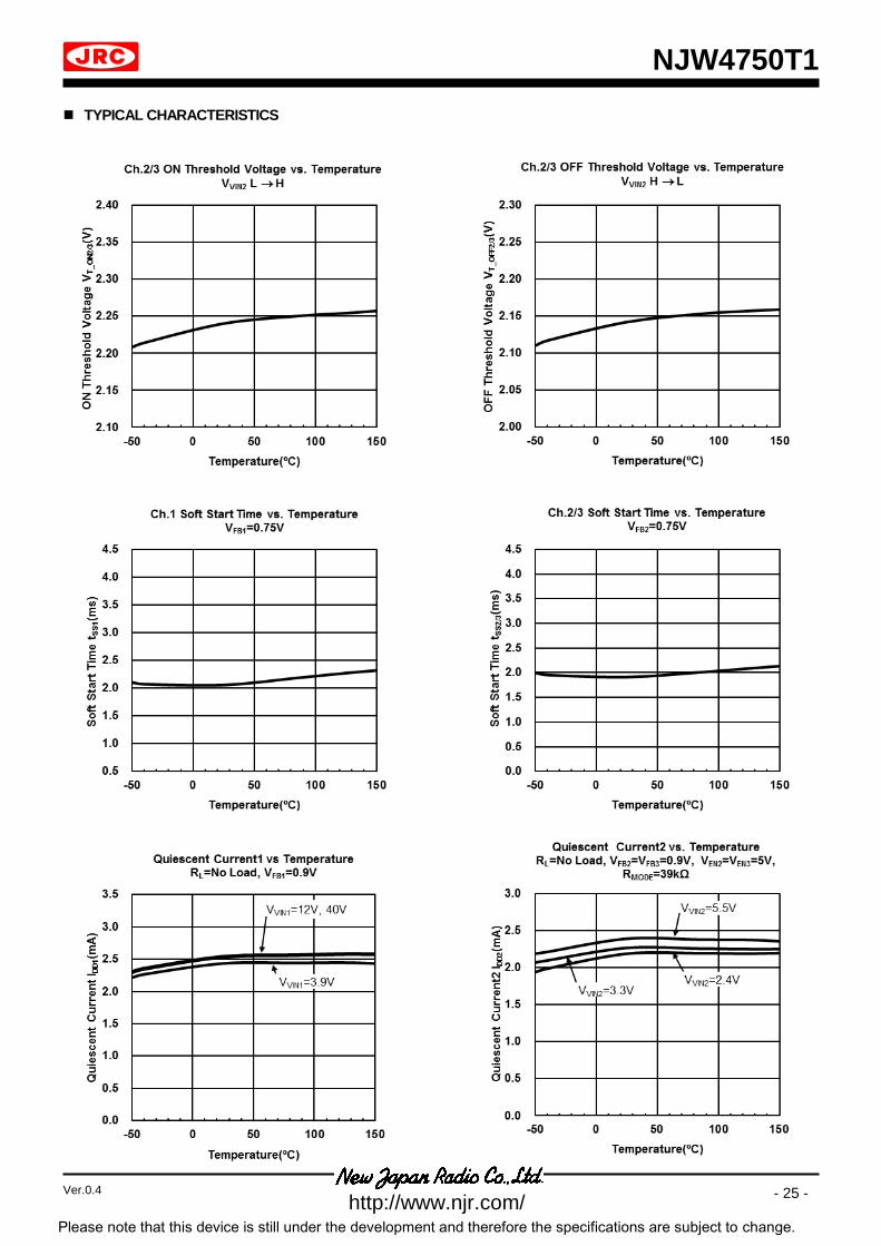
TYPICAL CHARACTERISTICS
NJW4750T1
- 25 - Ver.0.4
http://www.njr.com/ Please note that this device is still under the development and therefore the specifications are subject to change.
TYPICAL CHARACTERISTICS

NJW4750T1
- 26 - Ver.0.4
http://www.njr.com/ Please note that this device is still under the development and therefore the specifications are subject to change.
TYPICAL CHARACTERISTICS

NJW4750T1
- 27 - Ver.0.4
http://www.njr.com/ Please note that this device is still under the development and therefore the specifications are subject to change.
TYIPICAL CHARACTERISTICS
NJW4750T1
- 28 - Ver.0.4
http://www.njr.com/ Please note that this device is still under the development and therefore the specifications are subject to change.
INTRODUCTION
Please note the following when using NJW 4750.
The NJW 4750 can operate each Ch. independently.
However, even if Ch.1 is not used, it is necessary to input a power supply to VIN1.
Ch.3 (LDOMODE) and Ch.4 need to be start-up after power Ch. becomes active.
The LDO may not be start-up by the protection function.
e.g. The case of using Ch.1 as a power supply for Ch.4
It becomes the start of Ch.4 after normal start of Ch.1 by connecting PG1 of Ch.1 to EN4 of Ch.4.
PIN DESCRIPTION
PIN NO. SYMBOL DESCRIPTION
1 GND Ground pin
2 EN3 This pin controls the operation and stop of Ch.3. High Level: operation, Low level or Open level: Standby mode.
3 FB3 This pin detects the output voltage of Ch.3.
The output voltage is divided and inputted so that the FB pin voltage becomes 0.8V same as the reference voltage.
4 NC Non connection
5 FB2 This pin detects the output voltage of Ch.2.
The output voltage is divided and input so that the FB pin voltage become 0.8V same as the reference voltage.
6 EN2 This pin controls the operation and stop of Ch.2. High Level: operation, Low level or Open level: Standby mode.
7 RT Oscillation frequency setting pin by Timing Resistor. Oscillating frequency should set between 280kHz and 2.4MHz.
8 GND Ground pin
9 PG1 Power-good output of Ch.1 configured with open drain.
10 MODE This terminal is used to determine the operation mode. Connect an open or mode setting resistor.
11 FB1 This pin detects the output voltage of Ch.1.
The output voltage is divided and input so that the FB pin voltage become 0.8V same as the reference voltage.
12 EN1/SYNC This pin controls the operation and stop of Ch.1.High Level: operation, Low level or Open level: Standby mode.
By inputting the clock signal, it operates synchronized with the input signal.
13 VIN1 Power supply input for IC and Ch.1.
Since the impedance of the power supply path needs to be lowered connecting a capacitor (CIN) near the IC is required.
14 GND Ground
15 SW1 Ch.1 Output
16 EN4 This pin controls the operation and stop of Ch.4. High Level: operation, Low level or Open level: Standby mode.
17 LDOVOUT Ch.4 Output
18 FB4 This pin detects the output voltage of Ch.4.
The output voltage is divided and input so that the FB pin voltage become 0.8V same as the reference voltage.
19 LDOVIN Power supply input for Ch.4.
Since the impedance of the power supply path needs to be lowered connecting a capacitor (CIN) near the IC is required.
20 PG4 Power-good output of Ch.4 configured with open drain.
21 GND Ground
22 SW2 Ch.2 Output
23 PG2 Power-good output of Ch.2 configured with open drain.
24 VIN2 Power supply input for Ch.2 and Ch.3.
Since the impedance of the power supply path needs to be lowered connecting a capacitor (CIN) near the IC is required.
25 PG3 Power-good output of Ch.3 configured with open drain.
26 SW3 Ch.3 Output
Exposed
PAD - Exposed PAD on backside should be connected to the ground and soldered to PCB.
Technical Information

NJW4750T1
- 29 - Ver.0.4
http://www.njr.com/ Please note that this device is still under the development and therefore the specifications are subject to change.
DESCRIPTION OF BLOCK FEATURES
1. MODE SETTING
By connecting the resistor between the Mode pin and GND, the operation mode of Ch.3 and protection type of OCP are
selected.
The mode setting can be set only at startup, and the state of the mode can be checked by terminal voltage.
2. Basic Functions of switching regulator. (Ch.1,2 and Ch.3 are similar)
Error Amplifier Section (Error AMP)
0.8V±1% precise reference voltage is connected to the non-inverted input of this section.
Output voltage can be set by connection of converter's output to inverted input of this section (FB pin).
If the output voltage over 0.8V is required, a resistor divider must be inserted.
PWM Comparator Section (PWM), Oscillating Circuit Section (OSC)
Oscillating frequency can be set by inserting resistor between the RT pin and GND.
Table 1 shows example of oscillating frequency and timing resistor. The resistance is adapted to a series of E24 and a
series of E96
Please set the oscillating frequency according to Table.1
Table 1. NJW4750 oscillating frequency and timing resistor
Oscillating
Frequency
(kHz)
Timing
Resistor
(k)
Oscillating
Frequency
(kHz)
Timing
Resistor
(k)
280 27 2100 2.7
380 20 2200 2.4
500 15 2300 2.0
700 10 2400 1.8
1000 6.8
1200 5.6
1800 3.9
2000 3.0
NJW4750 is limited in minimum ON time tON-min=80ns typ. and minimum OFF time tOFF -min=100ns typ.
Max duty is 100%.
When you design the application, please refer to "Application information - Setting of the oscillating frequency".
MODE
Setting resistor
RMODE(±5%) CH3 OCP Mode
MODE PIN
Output Voltage
(±5%) Min Max
1 open LDO. Latch 2.5V
2 82kΩ 110kΩ SW reg. Latch 1.4V
3 27kΩ 39kΩ SW reg. Hiccup(SW)
Foldback(LDO) 1.2V
4 6.8kΩ 15k LDO Hiccup(SW)
Foldback(LDO) 1.0V
Technical Information

NJW4750T1
- 30 - Ver.0.4
http://www.njr.com/ Please note that this device is still under the development and therefore the specifications are subject to change.
DESCRIPTION OF BLOCK FEATURES (Continued)
Power MOSFET
The power is stored in the inductor by the switch operation of built-in power MOSFET. The output current is limited by
the overcurrent protection function.
Maximum rating of the SW terminal is defined by potential difference with the input voltage.
Power Supply, GND pin(VIN、GND)
Current flows into the IC according to drive frequency in a switching element. When impedance of a power supply line
is high, power supply will be unstably, and the performance of the IC can't be drawn out sufficiently.
Therefore, since the impedance of the power supply path needs to be lowered connecting a capacitor (CIN) near the IC
is required.
3. Additional and Protection Functions of switching regulator. (Ch.1,2 and Ch.3 are similar)
Under Voltage Lockout (UVLO)
The UVLO circuit stops the IC operation in a low power supply voltage case, and when a power supply voltage be-
comes higher voltage than threshold, then the IC operation starts.
The threshold voltage has a hysteresis voltage width at rising and falling. A flutter of detection and release of UVLO is
prevented by it.
Soft start function
The output voltage of the converter gradually rises to a set value by the soft start function. The soft start time is 4ms
(max.). It is defined with the time of the error amplifier reference voltage becoming from 0V to 0.75V.(Fig.1)
Soft start operating condition.
・ Ch.1: VVIN1≧VT_ON1、VEN1≧VTHH_EN1
・ Ch.2: VVIN1≧VT_ON1、VVIN2≧VT_ON2、VEN2≧VTHH_EN2
・ Ch.3: VVIN1≧VT_ON1、VVIN2≧VT_ON2、VEN3≧VTHH_EN3
Also thermal shutdown must be disabled.
Fig.1. Soft start timing chart
Technical Information
NJW4750T1
- 31 - Ver.0.4
http://www.njr.com/ Please note that this device is still under the development and therefore the specifications are subject to change.
DESCRIPTION OF BLOCK FEATURES (Continued)
Over Current Protection Circuit (OCP) (Ch.1,2 and Ch.3 are similar)
Switching regulator block of NJW4750 has 2 kinds of overcurrent protection function.
1. Hiccup (fig.2):
Switching operation is reduced and output is restricted. When the load state normally returns, it is reset auto-
matically.
2. Latch (Fig.3):
The function as the power supply is suspended. Manual return by re input of EN or VIN.
※ Hiccup system is each Ch. Independent control. Latch system suspends all output of IC.
Operating condition of OCP
In the soft start operating, Hiccup/Latch becomes ineffective.
The overcurrent protection function operates when one of them of 2 conditions was formed.
VFBx<0.4V and 7cycle over current detection continuously.
Overcurrent detection continuously of 1/fosc×16×15 s.
Fig.2. Hiccup mode OCP timing chart
Fig.3. Latch mode OCP timing chart
Technical Information

NJW4750T1
- 32 - Ver.0.4
http://www.njr.com/ Please note that this device is still under the development and therefore the specifications are subject to change.
DESCRIPTION OF BLOCK FEATURES (Continued)
External Clock Synchronization (Ch.1,2 and Ch.3 are similar)
By inputting a square wave to EN1/SYNC pin, the oscillator of NJW4750 can be synchronized to an external frequen-
cy.
The input square wave must be on the following specification. (Table 2.)
Table 2. The input square wave to EN1/SYNC pin.
Condition
Input Frequency fOSC0.9 to fOSC1.7
Upper limit 2,800kHz
Duty Cycle 25% to 75%
Voltage
magnitude
1.6V or more (High level)
0.4V or less (Low level)
Fig.4. Switching Operation by External Synchronized Clock
Technical Information

NJW4750T1
- 33 - Ver.0.4
http://www.njr.com/ Please note that this device is still under the development and therefore the specifications are subject to change.
DESCRIPTION OF BLOCK FEATURES (Continued)
4. Basic Functions of LDO (Ch.3 LDO mode and Ch.4)
Error Amplifier Section (Error AMP)
0.8V±1% precise reference voltage is connected to the non-inverted input of this section.
Output voltage can be set by connect converter's output to inverted input of this section (FB pin).
If requires output voltage over 0.8V, inserts resistor divider.
5. Additional and Protection Functions of LDO (Ch.3 LDO mode and Ch.4)
Over Current Protection Circuit(OCP)
LDO block of NJW4750 can choose 2 kinds of overcurrent protection function.
1. Fold back:
Limits the output current as the output voltage decreases.
2. Latch: The function as the power supply is suspended at FBpin voltage <0.4V.
Manual return by re input of EN or VIN.
※ Current limiting system is each Ch. Latch system suspends all output of IC.
6. Common Protection Function / Features
Thermal Shutdown Function (TSD)
When junction temperature of the NJW4750 exceeds the 160°C*, internal thermal shutdown circuit function stops SW
function. When junction temperature decreases to 145°C* or less, SW operation re-start from the soft start operation.
The purpose of this function is to prevent malfunctioning of IC at the high junction temperature.
Therefore it is not something that urges positive use. Please make sure to operate within the junction temperature
range rated (150°C). (* Design value)
Standby Function
Each Ch. stops the operating and becomes standby status when the ENx/(SYNC) pin becomes less than 0.4V.
The ENx/(SYNC) pins are internally pulled down with resistor (CH1 :5MΩ、CH2 :500k、CH3 :500k、CH4 :500k),
therefore the NJW4750 becomes standby mode when it is OPEN. Please connect this pin to VINx when you do not
use standby function.
Technical Information

NJW4750T1
- 34 - Ver.0.4
http://www.njr.com/ Please note that this device is still under the development and therefore the specifications are subject to change.
DESCRIPTION OF BLOCK FEATURES (Continued)
Power Good Function
It monitors the output status and outputs a signal from PG pin that is internally connected to an open drain of MOSFET.
If the FB terminal is within the range of -7% to + 15% of the error amplifier reference voltage, the PG terminal becomes
high impedance and notifies that the output voltage is normal. Otherwise the PG terminal becomes low level and tells
the output voltage is abnormal.
After soft start time, the Power Good function becomes effective in Ch.1, Ch.2, and Ch.3.
The Power Good function of Ch.4 becomes effective after passage for 150μs from ENX: H(@LDOVIN=3.3V).
Latch mode: added 1/fosc×16×2500 s delay in the Last boot Ch.
Fig.5. Power Good Function timing Chart at Hiccup mode
Fig.6. Power Good Function timing Chart at Latch mode
Technical Information
NJW4750T1
- 35 - Ver.0.4
http://www.njr.com/ Please note that this device is still under the development and therefore the specifications are subject to change.
VIN:Input voltage
VOUT:Output voltage
VSWH:High-side saturation voltage
VL:Catch Diode Vf or Lo-side saturation voltage VSWL
APPLICATION INFORMATION(Switching regulator)
Oscillating Frequency Setting
When a switching regulator uses high oscillating frequency, a small inductor and capacitor are used. If oscillating fre-
quency is high, reduction of effeciency and a limit of the minimum ON time and minimum OFF time are demerit.
The buck converter of ON time and OFF time is decided the following formula.
tON=(VOUT+VL)
(VIN-VSWH+VL)×fOSC
[s]
tOFF=1
fOSC
-tON[s]
When the ON time becomes shorter than TON-MIN or OFF time becomes shorter than TOFF-MIN, a change of duty or pulse
skip operation may be performed in order to maintain output voltage at a stable state.
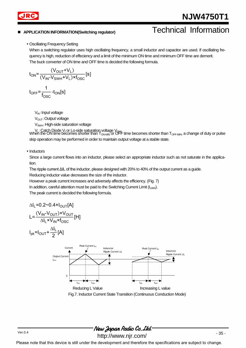
Inductors
Since a large current flows into an inductor, please select an appropriate inductor such as not saturate in the applica-
tion.
The ripple current ΔIL of the inductor, please designed with 20% to 40% of the output current as a guide.
Reducing inductor value decreases the size of the inductor.
However a peak current increases and adversely affects the efficiency. (Fig. 7)
In addition, careful attention must be paid to the Switching Current Limit (ILIMX).
The peak current is decided the following formula.
∆IL=0.2~0.4×IOUT[A]
L=(VIN-VOUT)×VOUT
∆IL×VIN×fOSC
[H]
Ipk=IOUT+∆IL
2[A]
Reducing L Value Increasing L value
Fig.7. Inductor Current State Transition (Continuous Conduction Mode)
Output Current
IOUT
Indunctor
Ripple Current IL
0
Current
tON tOFF
Peak Current IPK
Indunctor
Ripple Current IL
Peak Current IPK
tON tOFF
Technical Information
NJW4750T1
- 36 - Ver.0.4
http://www.njr.com/ Please note that this device is still under the development and therefore the specifications are subject to change.
APPLICATION INFORMATION(Switching regulator)
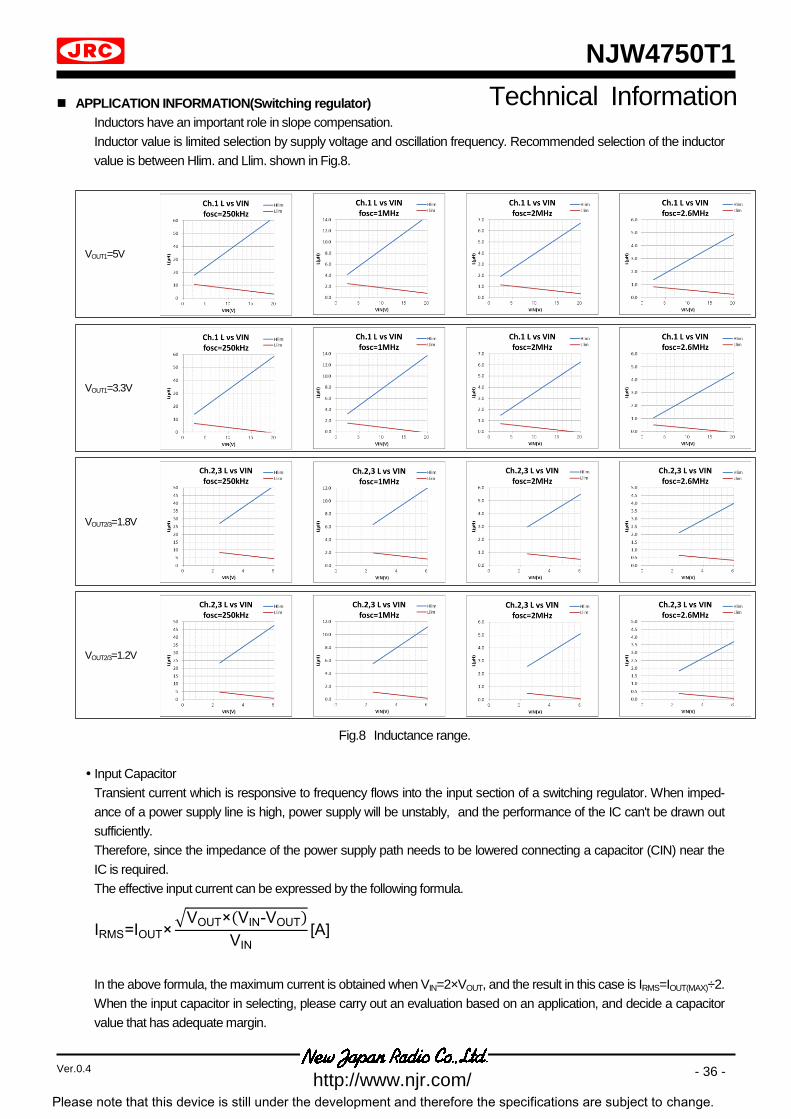
Inductors have an important role in slope compensation.
Inductor value is limited selection by supply voltage and oscillation frequency. Recommended selection of the inductor
value is between Hlim. and Llim. shown in Fig.8.
Fig.8 Inductance range.
Input Capacitor
Transient current which is responsive to frequency flows into the input section of a switching regulator. When imped-
ance of a power supply line is high, power supply will be unstably, and the performance of the IC can't be drawn out
sufficiently.
Therefore, since the impedance of the power supply path needs to be lowered connecting a capacitor (CIN) near the
IC is required.
The effective input current can be expressed by the following formula.
IRMS=IOUT×√VOUT×(VIN-VOUT)
VIN
[A]
In the above formula, the maximum current is obtained when VIN=2×VOUT, and the result in this case is IRMS=IOUT(MAX)÷2.
When the input capacitor in selecting, please carry out an evaluation based on an application, and decide a capacitor
value that has adequate margin.
Technical Information
VOUT1=5V
VOUT1=3.3V
VOUT2/3=1.8V
VOUT2/3=1.2V
NJW4750T1
- 37 - Ver.0.4
http://www.njr.com/ Please note that this device is still under the development and therefore the specifications are subject to change.
APPLICATION INFORMATION(Switching regulator)
Output Capacitor
An output capacitor stores power from the inductor, and stabilizes voltage provided to the output.
The NJW4750 is designed phase compensation so that output capacitor of low ESR can be used. Therefore a ce-
ramic capacitor is the most suitable.
Since capacity of a ceramic capacitor may decline by DC supply voltage and temperature change, please confirm it's
characteristics on specification sheet.
When selecting an output capacitor, must be considered Equivalent Series Resistance (ESR) characteristics, ripple
current, and breakdown voltage.
In case of using a low ESR capacitor, it's possible to lower the ripple voltage.
The output ripple noise can be expressed by the following formula.
Vripple(p-p)=∆IL× (ESR+1
8×fOSC×COUT
) [V]
The effective ripple current that flows in a capacitor (Irms) is obtained by the following equation.
IRMS=∆IL
2√3[ARMS]
Setting of phase compensation
The NJW 4750 has a built-in phase compensation circuit.
Table 3 shows the values of external parts based on oscillation frequency and output voltage.
Table. 3 Value of Phase compensation
* VVIN2 is 4 V or less.
If VVIN2 is set to higher than 4 V, the oscillating frequency is limited up to 1.5MHz.
Technical Information
fOSC VOUT COUT CFB RFB R2
2.5V, 2.8V, 3.3V,
3.6V, 5V 10μF or more 22pF 1kΩ 30kΩ to 75kΩ
1.8V 22μF or more 22pF 1kΩ 30kΩ to 75kΩ
1.1V*, 1.2V* 47μF or more 22pF 1kΩ 30kΩ to 75kΩ
500kHz or less ALL 100μF or more open open 30kΩ to 75kΩ
1MHz or more

NJW4750T1
- 38 - Ver.0.4
http://www.njr.com/ Please note that this device is still under the development and therefore the specifications are subject to change.
APPLICATION INFORMATION(Switching regulator)
Catch Diode
When the switch element is in OFF cycle, the power stored in the inductor flows to the output capacitor via the catch
diode. Therefore an electric current according to the load current flows to the diode every cycle. Since a diode's forward
saturation voltage and current accumulation cause power loss, a Schottky Barrier Diode (SBD), which has a low for-
ward saturation voltage, is most suitable.
When select the SBD, the reverse current at the high temperature is important, too.
The characteristic of SBD has a high reverse current than a general diode. If the reverse current is large, it leads to
the loss of the diode, so check the specification of the SBD
Setting Output Voltage, Compensation Capacitor
The output voltage VOUT is determined by the relative resistances of R1, R2.
VOUT= (R2
R1+1)×VB[A]
Fig.9. Output voltage setting(switching)
Technical Information

NJW4750T1
- 39 - Ver.0.4
http://www.njr.com/ Please note that this device is still under the development and therefore the specifications are subject to change.
APPLICATION INFORMATION(Switching regulator)
Board Layout
In the switching regulator application, since the current flow corresponds to the oscillating frequency, the substrate
(PCB) layout is very important.
Therefore, a current flowing line must be wide and short as much as possible. Fig.10. shows a current loop of a
step-down converter. (In case of synchronous rectification, SBD is changed to built-in SW.)
Especially, the loop of CIN - SW - SBD which has a high frequency switching, is necessary to consider minimize loop
at first. It is effective in reducing of spike noise caused by parasitic inductor.
(a) Buck Converter SW ON (b) Buck Converter SW OFF
Fig.10. Current Loop of Buck Converter
About concerning the GND, it is preferred to separate the power GND and the signal GND, and use single ground
point.
The voltage sensing feedback line should be away as far away as possible from the inductor. Since this line has high
impedance, it is laid out to avoid the influence noise caused by leakage flux from the inductor.
Fig. 11. shows example of wiring at buck converter.
Fig.11.Board Layout for Buck Converter
NJW4750 Built-in SW
COUT
L
SBD CIN VIN
NJW4750 Built-in SW
COUT
L
SBD CIN VIN
Since FB pin is high impedance, the
voltage detection resistance: R1/R2 is
placed from IC(FB) as near as possible.
To avoid the influence of the voltage
drop, the output voltage should be
detected near the load.
Separate Signal GND
from Power GND
Technical Information
NJW4750T1
- 40 - Ver.0.4
http://www.njr.com/ Please note that this device is still under the development and therefore the specifications are subject to change.
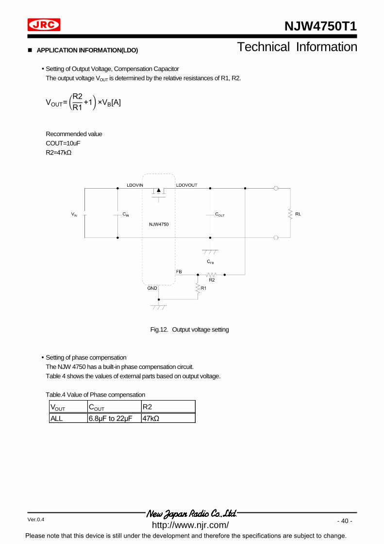
APPLICATION INFORMATION(LDO)
Setting of Output Voltage, Compensation Capacitor
The output voltage VOUT is determined by the relative resistances of R1, R2.
VOUT= (R2
R1+1)×VB[A]
Recommended value
COUT=10uF
R2=47kΩ
Fig.12. Output voltage setting
Setting of phase compensation
The NJW 4750 has a built-in phase compensation circuit.
Table 4 shows the values of external parts based on output voltage.
Table.4 Value of Phase compensation
VOUT COUT R2
ALL 6.8μF to 22μF 47kΩ
Technical Information

NJW4750T1
- 41 - Ver.0.4
http://www.njr.com/ Please note that this device is still under the development and therefore the specifications are subject to change.
CALCULATION OF PACKAGE POWER
The loss of NJW 4750 is the sum of the loss due to switching converter and the loss due to LDO.
Switching convertor
Input power :PIN = VIN IIN [W]
Output power :POUT = VOUT IOUT [W]
Diode loss :PDIODE = VF IL(avg) OFF duty [W]
Power Consumption :PLOSS = PIN POUT PDIODE [W]
Where:
VIN :Input Voltage of Converter IIN :Input Current of Converter
VOUT :Output Voltage of Converter IOUT :Output Current of Converter
VF :Diode's Forward Saturation Voltage IL(avg) :Inductor Average Current
OFF duty :Switch OFF Duty cycle
LDO
Input power :PIN = VIN IIN [W]
Output power :POUT = VOUT IOUT [W]
Power Consumption :PLOSS = PIN POUT [W]
Where:
VIN :Input Voltage of LDO IIN :Input Current of LDO
VOUT :Output Voltage of LDO IOUT :Output Current of LDO
Efficiency (η) is calculated as follows. = (POUT PIN) 100 [%]
Please consider temperature derating to the calculated power consumption: P D .
Please consider design power consumption in rated range referring to the power dissipation vs. ambient temperature
characteristics.
Technical Information

NJW4750T1
- 42 - Ver.0.4
http://www.njr.com/ Please note that this device is still under the development and therefore the specifications are subject to change.
APPLICATION DESIGN EXAMPLES
Spec
IC: NJW4750
OUTPUT: 3.3V (Ch.1)
1.8V (Ch.2)
1.2V (Ch.3)
2.8V (Ch.4)
Oscillating frequency: 2.1MHz
Schematic
Parts list
Technical Information
Ref. Part name Overview Maker
IC NJW4750MHH-T1 Quad Channel Combination Regulator NJRCCIN1 CGA4J3X5R1H475K125AB Ceramic Capacitor 2012 4.7uF, 50V TDKCIN2 GRM21BB31C106KE15L Ceramic Capacitor 2125 10uF, 16V MURATA
CLDOIN GRM21BB31C106KE15L Ceramic Capacitor 2125 10uF, 16V MURATAR3 2.4kΩ Resistor 1608 2.4kΩ, ±1%, 0.1W Std.L1 VLS4012ET-1R5N inductor 1.5uH, 2.1A TDK
SBD CMS14 Schottky Diode 60V, 2A TOSHIBACOUT1 GRM21BB31C106KE15L Ceramic Capacitor 2125, 10uF, 16V MURATACFB1 22pF Ceramic Capacitor 22pF, 50V Std.RFB1 1kΩ Resistor 1kΩ, ±1%, 0.1W Std.R11 24.3kΩ Resistor 24.3kΩ, ±1%, 0.1W Std.R12 76.8kΩ Resistor 76.8kΩ, ±1%, 0.1W Std.L2 VLS3015ET-2R2M inductor 2.2uH, 1.5A TDK
COUT2 GRM21BB30J226ME38L Ceramic Capacitor 2012 22uF, 6.3V MURATACFB2 22pF Ceramic Capacitor 22pF, 50V Std.RFB2 1kΩ Resistor 1kΩ, ±1%, 0.1W Std.R21 24kΩ Resistor 24kΩ, ±1%, 0.1W Std.R22 30kΩ Resistor 30kΩ, ±1%, 0.1W Std.L3 VLS3015ET-2R2M inductor 2.2uH, 1.5A TDK
COUT3 JMK212BBJ476MG-T Ceramic Capacitor 2012 47uF, 6.3V TAIYO YUDENCFB3 22pF Ceramic Capacitor 22pF, 50V Std.RFB3 1kΩ Resistor 1kΩ, ±1%, 0.1W Std.R31 75kΩ Resistor 75kΩ, ±1%, 0.1W Std.R32 37.4kΩ Resistor 37.4kΩ, ±1%, 0.1W Std.
CLDOOUT GRM21BB31C106KE15L Ceramic Capacitor 2125 10uF, 16V MURATAR1 18.7kΩ Resistor 18.7kΩ, ±1%, 0.1W Std.R2 47.5kΩ Resistor 47.5kΩ, ±1%, 0.1W Std.R4 10kΩ Resistor 10kΩ, ±1%, 0.1W Std.
RMODE 35.7kΩ Resistor 35.7kΩ, ±1%, 0.1W SW_Hiccup MODE
NJW4750T1
- 43 - Ver.0.4
http://www.njr.com/ Please note that this device is still under the development and therefore the specifications are subject to change.
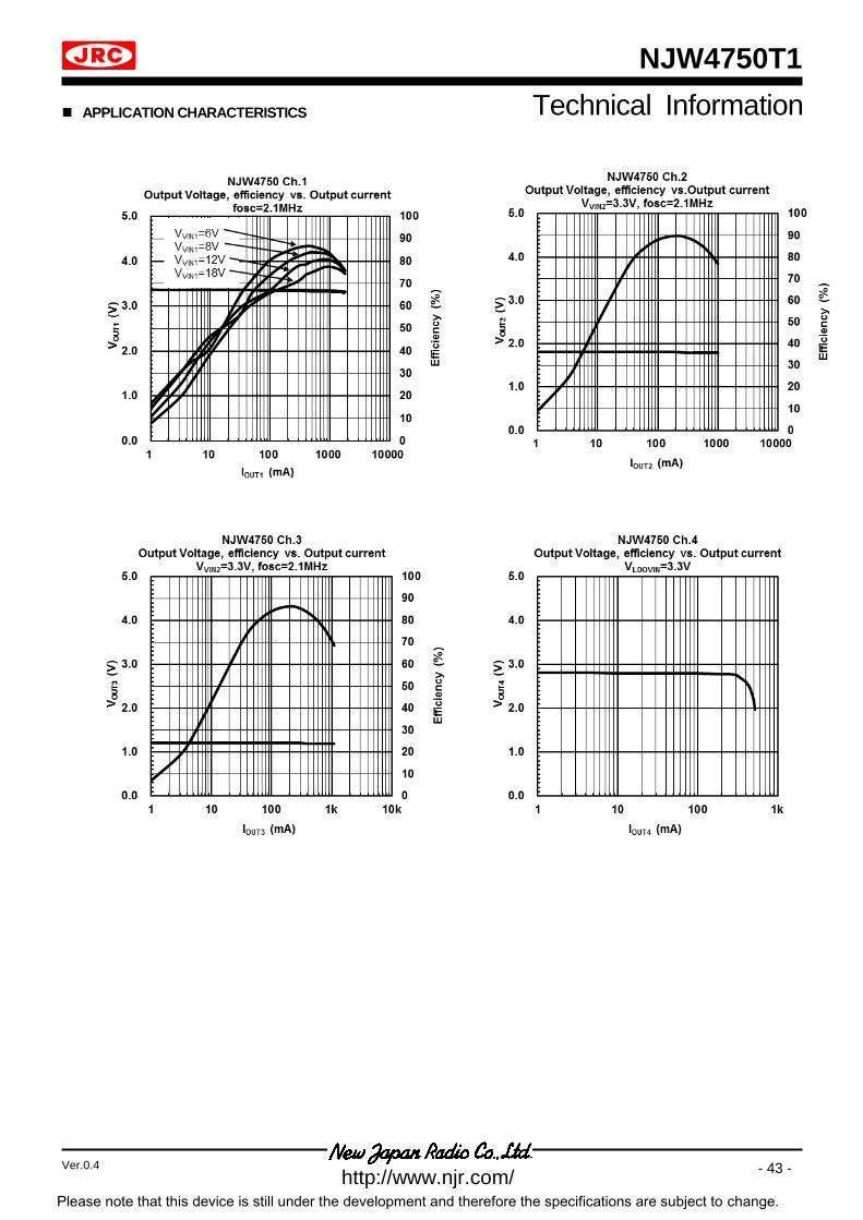
APPLICATION CHARACTERISTICS
Technical Information

NJW4750T1
- 44 - Ver.0.4
http://www.njr.com/ Please note that this device is still under the development and therefore the specifications are subject to change.
PACKAGE/ FOOTPATTERN
PACKAGE DIMENSIONS
EXAMPLE OF SOLDER PADS DIMENSIONS +0.010
-0.008
0.7±
0.05
3.4±0.05
2.6±
0.05
0.2 S
0.01
S
0.05 S
1.59±
0.05
0.21±
0.05
2.39±0.05
B
A
C0.4
3-R0.4
0.4
0.2±0.050.05 M S AB
2.32
3.6
1.52
2.8
0.4
0.2
0.1
0.1 0.2 0.4
0.31
R0.37
Unit: mm
NJW4750T1
- 45 - Ver.0.4
http://www.njr.com/ Please note that this device is still under the development and therefore the specifications are subject to change.
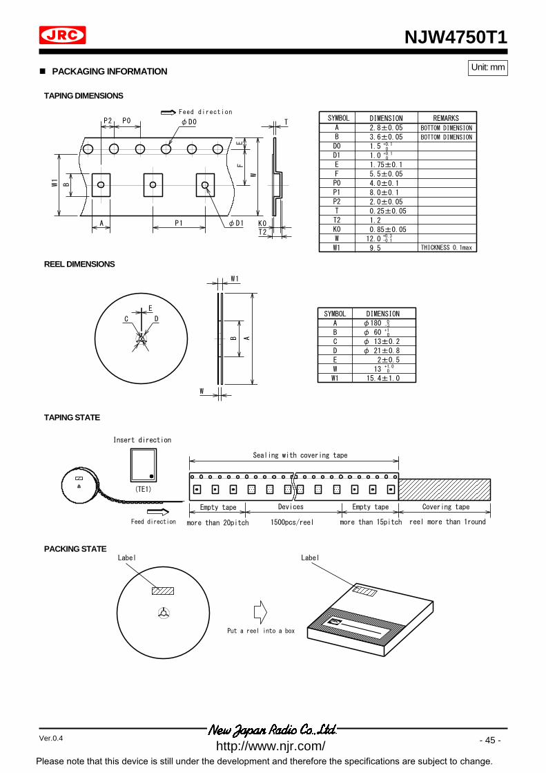
PACKAGING INFORMATION
TAPING DIMENSIONS
Feed direction
A
BW1
P2 P0 φD0
P1
EF
W
T
K0T2
φD1
SYMBOL
AB
D0D1EFP0P1P2TT2K0WW1
DIMENSION
2.8±0.053.6±0.051.51.01.75±0.15.5±0.054.0±0.18.0±0.12.0±0.050.25±0.051.20.85±0.0512.09.5
REMARKS
BOTTOM DIMENSION
BOTTOM DIMENSION
THICKNESS 0.1max
+0.10
+0.10
+0.3-0.1
REEL DIMENSIONS
A
E
C D
B
W
W1
SYMBOLA
BC
DE
WW1
DIMENSIONφ180
φ 60φ 13±0.2
φ 21±0.82±0.5
1315.4±1.0
0-3+10
+1.00
TAPING STATE
Feed direction
Sealing with covering tape
Empty tape Devices Empty tape Covering tape
more than 20pitch 1500pcs/reel more than 15pitch reel more than 1round
PACKING STATE
Put a reel into a box
LabelLabel
Insert direction
(TE1)
Unit: mm

NJW4750T1
- 46 - Ver.0.4
http://www.njr.com/ Please note that this device is still under the development and therefore the specifications are subject to change.
a:Temperature ramping rate : 1 to 4°C /s
b:Pre-heating temperature
time
: 150 to 180°C : 60 to 120s
c:Temperature ramp rate : 1 to 4°C /s
d:220℃ or higher time : Shorter than 60s
e:230℃ or higher time : Shorter than 40s
f:Peak temperature : Lower than 260°C
g:Temperature ramping rate : 1 to 6°C /s
The temperature indicates at the surface of mold package.
RECOMMENDED MOUNTING METHOD
INFRARED REFLOW SOLDERING METHOD
Recommended reflow soldering procedure
a b c
e
g
150°C
260°C
Room Temp.
f
180°C
230°C
220°C d

NJW4750T1
- 47 - Ver.0.4
http://www.njr.com/ Please note that this device is still under the development and therefore the specifications are subject to change.
REVISION HISTORY
DATE REVISION CHANGES
2017.11.7 Ver.0.1 Revise product preview
2017.12.15 Ver.0.2 Revise part list
2018.2.15 Ver.0.3
Revise ELECTRICAL CHARACTERISTICS
Page.6, 9, 13 Minimum OFF Time
Page 6, 9, 13 Minimum ON Time
Page 14, 15 Ripple Rejection
2018.2.21 Ver.0.4 Add comment to application information.
P37

NJW4750T1
- 48 - Ver.0.4
http://www.njr.com/ Please note that this device is still under the development and therefore the specifications are subject to change.
[ CAUTION ]
1. New JRC strives to produce reliable and high quality semiconductors. New JRC's semiconductors are intended for specific
applications and require proper maintenance and handling. To enhance the performance and service of New JRC's semicon-
ductors, the devices, machinery or equipment into which they are integrated should undergo preventative maintenance and in-
spection at regularly scheduled intervals. Failure to properly maintain equipment and machinery incorporating these products
can result in catastrophic system failures
2. The specifications on this datasheet are only given for information without any guarantee as regards either mistakes or omis-
sions. The application circuits in this datasheet are described only to show representative usages of the product and not in-
tended for the guarantee or permission of any right including the industrial rights.
All other trademarks mentioned herein are property of their respective companies.
3. To ensure the highest levels of reliability, New JRC products must always be properly handled.
The introduction of external contaminants (e.g. dust, oil or cosmetics) can result in failures of semiconductor products.
4. New JRC offers a variety of semiconductor products intended for particular applications. It is important that you select the
proper component for your intended application. You may contact New JRC's Sale's Office if you are uncertain about the
products listed in this catalog.
5. Special care is required in designing devices, machinery or equipment which demand high levels of reliability. This is particu-
larly important when designing critical components or systems whose failure can foreseeably result in situations that could
adversely affect health or safety. In designing such critical devices, equipment or machinery, careful consideration should be
given to amongst other things, their safety design, fail-safe design, back-up and redundancy systems, and diffusion design.
6. The products listed in the catalog may not be appropriate for use in certain equipment where reliability is critical or where the
products may be subjected to extreme conditions. You should consult our sales office before using the products in any of the
following types of equipment.
Aerospace Equipment
Equipment Used in the Deep sea
Power Generator Control Equipment (Nuclear, Steam, Hydraulic)
Life Maintenance Medical Equipment
Fire Alarm/Intruder Detector
Vehicle Control Equipment (airplane, railroad, ship, etc.)
Various Safety devices
7. New JRC's products have been designed and tested to function within controlled environmental conditions. Do not use
products under conditions that deviate from methods or applications specified in this catalog. Failure to employ New JRC
products in the proper applications can lead to deterioration, destruction or failure of the products. New JRC shall not be re-
sponsible for any bodily injury, fires or accident, property damage or any consequential damages resulting from misuse or
misapplication of its products. Products are sold without warranty of any kind, either express or implied, including but not lim-
ited to any implied warranty of merchantability or fitness for a particular purpose.
8. Warning for handling Gallium and Arsenic(GaAs) Products (Applying to GaAs MMIC, Photo Reflector). This Products uses Gal-
lium(Ga) and Arsenic(As) which are specified as poisonous chemicals by law. For the prevention of a hazard, do not burn, de-
stroy, or process chemically to make them as gas or power. When the product is disposed, please follow the related regulation
and do not mix this with general industrial waste or household waste.
9. The product specifications and descriptions listed in this catalog are subject to change at any time, without notice.
Related Documents

![Ch 10 95 [Rread-Only] [Compatibility Mode]](https://static.cupdf.com/doc/110x72/55cf8e86550346703b9311b1/ch-10-95-rread-only-compatibility-mode.jpg)

![Ch#12 Prdct [Compatibility Mode]](https://static.cupdf.com/doc/110x72/577d20171a28ab4e1e91f741/ch12-prdct-compatibility-mode.jpg)

![Ch 0 - Introduction [Compatibility Mode]](https://static.cupdf.com/doc/110x72/577d36fb1a28ab3a6b947dbf/ch-0-introduction-compatibility-mode.jpg)
![FInancial Intermediaries-Ch 3-Part I [Compatibility Mode]](https://static.cupdf.com/doc/110x72/543384f5219acd5f1a8b48c3/financial-intermediaries-ch-3-part-i-compatibility-mode.jpg)
![Ch 3. Unsur Dasar PHT [Compatibility Mode]](https://static.cupdf.com/doc/110x72/587f4db71a28abc8108b9361/ch-3-unsur-dasar-pht-compatibility-mode.jpg)
![Ch 8 95 [RRead-Only] [Compatibility Mode]](https://static.cupdf.com/doc/110x72/55cf8e86550346703b931043/ch-8-95-rread-only-compatibility-mode.jpg)

![Ch-01 [Compatibility Mode]](https://static.cupdf.com/doc/110x72/577d2dba1a28ab4e1eae2d22/ch-01-compatibility-mode.jpg)