DEVICE SPECIFICATIONS NI 6239 M Series Data Acquisition: 16-Bit, 250 kS/s, 8 AI, 2 AO, 24 DIO Sinking, Current Input/Output Bank Isolation The following specifications are typical at 25 °C, unless otherwise noted. For more information about the NI 6239, refer to the NI 6238/6239 User Manual available from ni.com/ manuals. Analog Input Number of channels 8 differential current inputs Ground reference AI GND ADC resolution 16 bits DNL No missing codes guaranteed INL Refer to the AI Absolute Accuracy section Sample rate Maximum 250 kS/s Minimum No minimum Timing accuracy 50 ppm of sample rate Timing resolution 50 ns Input coupling DC Input range ±20 mA Maximum working voltage for analog inputs Refer to the Maximum Working Voltage section Input impedance (AI+ to AI-) 92 Ω ±10% in parallel with 100 pF Maximum input impedance 100 Ω (at 55 °C) Input bias current ±100 pA Small signal bandwidth (-3 dB) 700 kHz Input FIFO size 4,095 samples Scan list memory 4,095 entries

Welcome message from author
This document is posted to help you gain knowledge. Please leave a comment to let me know what you think about it! Share it to your friends and learn new things together.
Transcript

DEVICE SPECIFICATIONS
NI 6239M Series Data Acquisition: 16-Bit, 250 kS/s, 8 AI, 2 AO, 24 DIOSinking, Current Input/Output Bank Isolation
The following specifications are typical at 25 °C, unless otherwise noted. For moreinformation about the NI 6239, refer to the NI 6238/6239 User Manual available from ni.com/manuals.
Analog InputNumber of channels 8 differential current inputs
Ground reference AI GND
ADC resolution 16 bits
DNL No missing codes guaranteed
INL Refer to the AI Absolute Accuracy section
Sample rate
Maximum 250 kS/s
Minimum No minimum
Timing accuracy 50 ppm of sample rate
Timing resolution 50 ns
Input coupling DC
Input range ±20 mA
Maximum working voltage for analoginputs
Refer to the Maximum Working Voltage section
Input impedance (AI+ to AI-) 92 Ω ±10% in parallel with 100 pF
Maximum input impedance 100 Ω (at 55 °C)
Input bias current ±100 pA
Small signal bandwidth (-3 dB) 700 kHz
Input FIFO size 4,095 samples
Scan list memory 4,095 entries

Data transfers DMA (scatter-gather), interrupts,programmed I/O
Input current during overvoltage condition ±20 mA maximum/AI pin
Overcurrent protection ±40 mA maximum1
Overvoltage protection (AI x+ or AI x- with respect to AI GND)2
Device on ±25 V for up to two AI pins
Device off ±15 V for up to two AI pins
Typical Performance GraphsFigure 1. AI Small Signal Bandwidth
Frequency (Hz)
Nor
mal
ized
Sig
nal A
mpl
itude
(dB
)
–14
–12
–10
–8
–6
–4
–2
0
2
1 k 10 k 100 k 1000 k 10000 k
1 Any voltage applied resulting in current flowing above 40 mA can damage the device permanently.2 This overvoltage protection triggers after the overcurrent protection is in effect.
2 | ni.com | NI 6239 Device Specifications
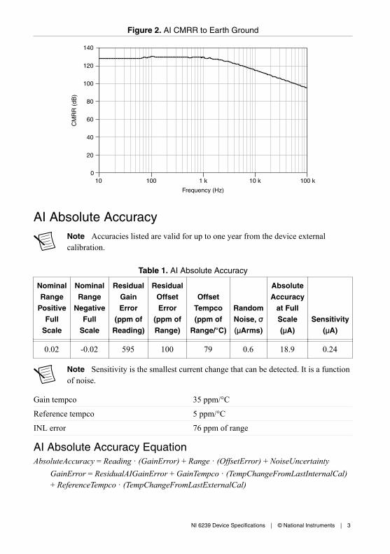
Figure 2. AI CMRR to Earth Ground
0
20
40
60
80
120
100
140
10 100 1 k 10 k 100 k
Frequency (Hz)
CM
RR
(dB
)
AI Absolute AccuracyNote Accuracies listed are valid for up to one year from the device externalcalibration.
Table 1. AI Absolute Accuracy
NominalRange
PositiveFull
Scale
NominalRange
NegativeFull
Scale
ResidualGainError
(ppm ofReading)
ResidualOffsetError
(ppm ofRange)
OffsetTempco(ppm of
Range/°C)
RandomNoise, σ(μArms)
AbsoluteAccuracy
at FullScale(μA)
Sensitivity(μA)
0.02 -0.02 595 100 79 0.6 18.9 0.24
Note Sensitivity is the smallest current change that can be detected. It is a functionof noise.
Gain tempco 35 ppm/°C
Reference tempco 5 ppm/°C
INL error 76 ppm of range
AI Absolute Accuracy EquationAbsoluteAccuracy = Reading · (GainError) + Range · (OffsetError) + NoiseUncertainty
GainError = ResidualAIGainError + GainTempco · (TempChangeFromLastInternalCal)+ ReferenceTempco · (TempChangeFromLastExternalCal)
NI 6239 Device Specifications | © National Instruments | 3

OffsetError = ResidualAIOffsetError + OffsetTempco ·(TempChangeFromLastInternalCal) + INLError
NoiseUncertainty = RandomNoise ⋅ 3100 for a coverage factor of 3 σ and averaging
100 points.
AI Absolute Accuracy ExampleAbsolute accuracy at full scale on the analog input channels is determined using the followingassumptions:• TempChangeFromLastExternalCal = 10 °C• TempChangeFromLastInternalCal = 1 °C• number_of_readings = 100• CoverageFactor = 3 σ
For example, on the 20 mA range, the absolute accuracy at full scale is as follows:GainError = 595 ppm + 35 ppm · 1 + 5 ppm · 10 = 680 ppmOffsetError = 100 ppm + 79 ppm · 1 + 76 ppm = 255 ppm
NoiseUncertainty = .6 µ ⋅ 3100 = .18 µA
AbsoluteAccuracy = 20 mA · (GainError) + 20 mA · (OffsetError) + NoiseUncertainty =18.9 µA
Analog OutputNumber of channels 2 current outputs
Ground reference AO GND
DAC resolution 16 bits
Maximum update rate
1 channel 500 kS/s
2 channels 450 kS/s per channel
Timing accuracy 50 ppm of sample rate
Timing resolution 50 ns
Output range 0 mA to 20 mA
Output coupling DC
Power-on state 0 mA
Power-on glitch None
Output FIFO size 8,191 samples shared among channels used
4 | ni.com | NI 6239 Device Specifications
Data transfers DMA (scatter-gather), interrupts,programmed I/O
AO waveform modes Non-periodic waveform, periodic waveformregeneration mode from onboard FIFO,periodic waveform regeneration from hostbuffer including dynamic update
External power supply 10 VDC to 30 VDC, refer to the figure
External power supply consumption 50 mA maximum, refer to the figure
Internal voltage drop 3 V maximum, refer to the figure
Maximum resistive load Up to 1 kΩ with 24 V power supply connected;refer to the figure
Figure 3. Analog Output
User- Provided Load
User- Provided
Power Supply
DAC
InternalVoltage
Drop
AO PowerSupply Pin
AO x
User-ProvidedAO GND
–
+
AO GND
Protection Open and short circuit
Slew rate 0.1 mA/μS
AO Absolute AccuracyAbsolute accuracy at full-scale numbers is valid immediately following internal calibrationand assumes the device is operating within 10 °C of the last external calibration.
Note Accuracies listed are valid for up to one year from the device externalcalibration.
NI 6239 Device Specifications | © National Instruments | 5

Table 2. AO Absolute Accuracy
NominalRange
PositiveFull Scale
(A)
NominalRange
NegativeFull Scale
(A)
ResidualGain Error
(% ofReading)
GainTempco(ppm/°C)
ResidualOffset
Error (ppmof Range)
OffsetTempco(ppm of
Range/°C)
AbsoluteAccuracy
at FullScale (μA)
0.02 0 0.1570 20 0.0537 8 52.3
Reference tempco 5 ppm/°C
INL error 128 ppm of range
Random noise 2 μA
AO Absolute Accuracy EquationAbsoluteAccuracy = OutputValue · (GainError) + Range · (OffsetError)
GainError = ResidualGainError + GainTempco · (TempChangeFromLastInternalCal) +ReferenceTempco · (TempChangeFromLastExternalCal)OffsetError = ResidualOffsetError + AOOffsetTempco ·(TempChangeFromLastInternalCal) + INLError
Digital I/O/PFI
Static CharacteristicsNumber of channels 10 total
Number of input channels 6 (PFI <0..5>/P0.<0..5>)
Number of output channels 4 (PFI <6..9>/P1.<0..3>)
Direction control Fixed, lines are unidirectional
PFI/Port 0/Port 1 FunctionalityPFI <0..5>/P0.<0..5> Static digital input, timing input
PFI <6..9>/P1.<0..3> Static digital output, timing output
Timing output sources Many AI, AO, counter timing signals
Debounce filter settings 125 ns, 6.425 µs, 2.56 ms, disable; high andlow transitions; selectable per input
6 | ni.com | NI 6239 Device Specifications

Digital Input (Port 0)Number of channels 6
Ground reference P0.GND
Input voltage range 0 V to 30 V
Minimum pulse width for timing signal 0.5 μs
Logic "0" level 0 V to 4 V
Logic "1" level 10 V to 30 V
Minimum input impedance 3.3 kΩ
Typical input current 7 mA at 24 V input, 2.5 mA at 8 V input
Maximum input current 9 mA
Propagation delay
Low to high 150 ns, typical
High to low 100 ns, typical
Digital Output (Port 1)Number of channels 4
Ground reference P1.GND
Device output type DO sink
The following figure shows PO.<0..5> and PI.<0..3> on the NI 6239 device.
NI 6239 Device Specifications | © National Instruments | 7

Figure 4. NI 6239 Digital I/O Connections
P1.<0..3>
P1.0
P1.VCC
P1.GND
P1.1
P1.GND
P0.0
P0.GND
P0.GND
P1.GND
Digital Isolators
Maximum external supply voltage(P1.VCC)
30 V
On state saturation voltage 1.6 V maximum at 350 mA
Off state leakage 50 µA
Maximum current 100 mA for each line for simultaneous usage,350 mA for single line usage
Minimum pulse width for timing signal(sink output)
1.25 µs
Propagation delay (sink output)
Open to close 0.4 µs
Close to open 0.4 µs
General-Purpose Counters/TimersNumber of counter/timers 2
Resolution 32 bits
Counter measurements Edge counting, pulse, semi-period, period,two-edge separation
8 | ni.com | NI 6239 Device Specifications

Position measurements X1, X2, X4 quadrature encoding withChannel Z reloading; two-pulse encoding
Output applications Pulse, pulse train with dynamic updates,frequency division, equivalent time sampling
Internal base clocks 80 MHz, 20 MHz, 0.1 MHz
External base clock frequency 0 MHz to 20 MHz
Base clock accuracy 50 ppm
Inputs Gate, Source, HW_Arm, Aux, A, B, Z,Up_Down
Routing options for inputs Any input PFI, RTSI, PXI_TRIG, PXI_STAR,many internal signals
FIFO 2 samples
Data transfers Dedicated scatter-gather DMA controller foreach counter/timer; interrupts;programmed I/O
Frequency GeneratorNumber of channels 1
Base clocks 10 MHz, 100 kHz
Divisors 1 to 16
Base clock accuracy 50 ppm
Output can be available on any output PFI or RTSI terminal.
Phase-Locked Loop (PLL)Number of PLLs 1
Reference signal PXI_STAR, PXI_CLK10, RTSI <0..7>
Output of PLL 80 MHz Timebase; other signals derived from80 MHz Timebase including 20 MHz and100 kHz Timebases
External Digital TriggersSource Any PFI, RTSI, PXI_TRIG, PXI_STAR
Polarity Software-selectable for most signals
NI 6239 Device Specifications | © National Instruments | 9

Analog input function Start Trigger, Reference Trigger,Pause Trigger, Sample Clock, Convert Clock,Sample Clock Timebase
Analog output function Start Trigger, Pause Trigger, Sample Clock,Sample Clock Timebase
Counter/timer function Gate, Source, HW_Arm, Aux, A, B, Z,Up_Down
Device-to-Device Trigger BusPCI RTSI <0..7>3
PXI PXI_TRIG <0..7>, PXI_STAR
Output selections 10 MHz Reference Clock, frequency generatoroutput, many internal signals
Debounce filter settings 125 ns, 6.425 μs, 2.56 ms, disable; high andlow transitions; selectable per input
Bus InterfacePCI/PXI 3.3 V or 5 V signal environment
The PXI device can be installed in PXI slots or PXI Express hybrid slots.
DMA channels 4, analog input, analog output, counter/timer 0,counter/timer 1
Power RequirementsCurrent draw from bus during no-load condition
+5 V 0.7 A
+12 V 20 mA
Current draw from bus during AI and AO overvoltage condition
+5 V 0.95 A
+12 V 20 mA
3 In other sections of this document, RTSI refers to RTSI <0..7> for the PCI devices orPXI_TRIG <0..7> for PXI devices.
10 | ni.com | NI 6239 Device Specifications

Physical CharacteristicsDimensions
PCI printed circuit board 9.7 cm × 15.5 cm (3.8 in. × 6.1 in.)
PXI printed circuit board Standard 3U PXI
Weight
PCI 103 g (3.6 oz)
PXI 144 g (5.1 oz)
I/O connector 37-pin D-SUB
CalibrationRecommended warm-up time 15 minutes
Calibration interval 1 year
Maximum Working VoltageMaximum working voltage refers to the signal voltage plus the common-mode voltage.
Channel-to-earth ground4
Continuous ≤30 Vrms/60 VDC Measurement Category I
Withstand ≤840 Vrms/1,200 VDC, verified by a 5 sdielectric withstand test
Channel-to-bus5
Continuous ≤30 Vrms/60 VDC Measurement Category I
Withstand ≤1,400 Vrms/1,950 VDC, verified by a 5 sdielectric withstand test
Analog channel-to-AI GND or AO GND(in the following figure, |Va - Vb|)
≤11 V, Measurement Category I
Digital channel-to-P1.GND or P0.GND (inthe following figure, |Vc - Vd| or |Ve - Vf|)
≤30 V, Measurement Category I
Measurement Category I is for measurements performed on circuits not directly connected tothe electrical distribution system referred to as MAINS voltage. MAINS is a hazardous liveelectrical supply system that powers equipment. This category is for measurements of voltages
4 In the figure, |Va – Vh|, |Vc – Vh|, and |Ve – Vh|.5 In the figure, |Va – Vg|, |Vc – Vg|, and |Ve – Vg|.
NI 6239 Device Specifications | © National Instruments | 11

from specially protected secondary circuits. Such voltage measurements include signal levels,special equipment, limited-energy parts of equipment, circuits powered by regulated low-voltage sources, and electronics.
Caution This device is rated for Measurement Category I and the voltage acrossthe isolation barrier is limited to no greater than 30 Vrms/60 VDC/42.4 Vpkcontinuous. These test and measurement circuits are not intended for directconnection to the MAINS building installations of Measurement Categories CAT II,CAT III, or CAT IV.
The following figure illustrates the maximum working voltage specifications.
Figure 5. NI 6239 Maximum Working Voltage
PXI/PCI-BusAI x/AO xVa
Vb AI GND/AO GND
Vh
VgBus
PFI <0..5>Vc
Vd P0.GND
PFI <6..9>Ve
Vf P1.GND
EnvironmentalOperating temperature 0 ºC to 55 ºC
Storage temperature -20 ºC to 70 ºC
12 | ni.com | NI 6239 Device Specifications
Humidity 10% RH to 90% RH, noncondensing
Maximum altitude 2,000 m
Pollution Degree (indoor use only) 2
Indoor use only.
Shock and Vibration (PXI Only)Operational shock 30 g peak, half-sine, 11 ms pulse (Tested in
accordance with IEC 60068-2-27. Test profiledeveloped in accordance withMIL-PRF-28800F.)
Random vibration
Operating 5 Hz to 500 Hz, 0.3 grms
Nonoperating 5 Hz to 500 Hz, 2.4 grms (Tested in accordancewith IEC 60068-2-64. Nonoperating testprofile exceeds the requirements ofMIL-PRF-28800F, Class 3.)
SafetyThis product is designed to meet the requirements of the following electrical equipment safetystandards for measurement, control, and laboratory use:• IEC 61010-1, EN 61010-1• UL 61010-1, CSA 61010-1
Note For UL and other safety certifications, refer to the product label or the OnlineProduct Certification section.
Electromagnetic CompatibilityThis product meets the requirements of the following EMC standards for electrical equipmentfor measurement, control, and laboratory use:• EN 61326-1 (IEC 61326-1): Class A emissions; Basic immunity• EN 55011 (CISPR 11): Group 1, Class A emissions• EN 55022 (CISPR 22): Class A emissions• EN 55024 (CISPR 24): Immunity• AS/NZS CISPR 11: Group 1, Class A emissions• AS/NZS CISPR 22: Class A emissions
NI 6239 Device Specifications | © National Instruments | 13

• FCC 47 CFR Part 15B: Class A emissions• ICES-001: Class A emissions
Note In the United States (per FCC 47 CFR), Class A equipment is intended foruse in commercial, light-industrial, and heavy-industrial locations. In Europe,Canada, Australia and New Zealand (per CISPR 11) Class A equipment is intendedfor use only in heavy-industrial locations.
Note Group 1 equipment (per CISPR 11) is any industrial, scientific, or medicalequipment that does not intentionally generate radio frequency energy for thetreatment of material or inspection/analysis purposes.
Note For EMC declarations and certifications, and additional information, refer tothe Online Product Certification section.
CE Compliance This product meets the essential requirements of applicable European Directives, as follows:• 2014/35/EU; Low-Voltage Directive (safety)• 2014/30/EU; Electromagnetic Compatibility Directive (EMC)• 2011/65/EU; Restriction of Hazardous Substances (RoHS)
Online Product CertificationRefer to the product Declaration of Conformity (DoC) for additional regulatory complianceinformation. To obtain product certifications and the DoC for this product, visit ni.com/certification, search by model number or product line, and click the appropriate link in theCertification column.
Environmental ManagementNI is committed to designing and manufacturing products in an environmentally responsiblemanner. NI recognizes that eliminating certain hazardous substances from our products isbeneficial to the environment and to NI customers.
For additional environmental information, refer to the Minimize Our Environmental Impactweb page at ni.com/environment. This page contains the environmental regulations anddirectives with which NI complies, as well as other environmental information not included inthis document.
14 | ni.com | NI 6239 Device Specifications

Waste Electrical and Electronic Equipment (WEEE)EU Customers At the end of the product life cycle, all NI products must bedisposed of according to local laws and regulations. For more information abouthow to recycle NI products in your region, visit ni.com/environment/weee.
电子信息产品污染控制管理办法(中国 RoHS)中国客户 National Instruments 符合中国电子信息产品中限制使用某些有害物
质指令(RoHS)。关于 National Instruments 中国 RoHS 合规性信息,请登录
ni.com/environment/rohs_china。(For information about China RoHScompliance, go to ni.com/environment/rohs_china.)
Device PinoutFigure 6. NI PCI/PXI-6239 Pinout
1
2
3
4
5
6
7
8
9
10
11
12
13
14
15
16
17
18
19
20
21
22
23
24
25
26
27
28
29
30
31
32
33
34
35
36
37
AI 0+/CAL+
AI 1–
AI GND
AI 2–
AI 3+
AI 4+
AI 5–
CAL–
AI 6–
AI 7–
NC
AO 1
PFI 0/P0.0 (Input)
P0.GND
PFI 3/P0.3 (Input)
PFI 5/P0.5 (Input)
PFI 6/P1.0 (Output)
PFI 8/P1.2 (Output)
P1.VCC
AI 0–
AI 1+
AI 2+
AI 3–
AI GND
AI 4–
AI 5+
AI 6+
AI 7+
AO POWER SUPPLY
AO 0
AO GND
PFI 1/P0.1 (Input)
PFI 2/P0.2 (Input)
PFI 4/P0.4 (Input)
P1.GND
PFI 7/P1.1 (Output)
PFI 9/P1.3 (Output)
NC = No Connect
NI 6239 Device Specifications | © National Instruments | 15

Refer to the NI Trademarks and Logo Guidelines at ni.com/trademarks for information on NI trademarks. Other product andcompany names mentioned herein are trademarks or trade names of their respective companies. For patents covering NIproducts/technology, refer to the appropriate location: Help»Patents in your software, the patents.txt file on your media, or theNational Instruments Patent Notice at ni.com/patents. You can find information about end-user license agreements (EULAs)and third-party legal notices in the readme file for your NI product. Refer to the Export Compliance Information at ni.com/legal/export-compliance for the NI global trade compliance policy and how to obtain relevant HTS codes, ECCNs, and otherimport/export data. NI MAKES NO EXPRESS OR IMPLIED WARRANTIES AS TO THE ACCURACY OF THE INFORMATIONCONTAINED HEREIN AND SHALL NOT BE LIABLE FOR ANY ERRORS. U.S. Government Customers: The data contained inthis manual was developed at private expense and is subject to the applicable limited rights and restricted data rights as set forthin FAR 52.227-14, DFAR 252.227-7014, and DFAR 252.227-7015.
© 2015—2016 National Instruments. All rights reserved.
375211C-01 Jun16
Related Documents