990624 DARPA DARPA Microsystems Technology Office MTO MTO Dr. Edgar J. Martinez Program Manager Microsystems Technology Office 3701 N. Fairfax Drive Arlington, VA 22203 Tel. (703) 696-7436 [email protected] Next Generation of Terahertz Next Generation of Terahertz Sources and Detectors Sources and Detectors

Welcome message from author
This document is posted to help you gain knowledge. Please leave a comment to let me know what you think about it! Share it to your friends and learn new things together.
Transcript
990624
DARPADARPAMicrosystems Technology Office
MTOMTO
Dr. Edgar J. MartinezProgram Manager
Microsystems Technology Office
3701 N. Fairfax Drive Arlington, VA 22203Tel. (703) 696-7436
Next Generation of Terahertz Next Generation of Terahertz Sources and DetectorsSources and Detectors
990624
DARPADARPAMicrosystems Technology Office
MTOMTO
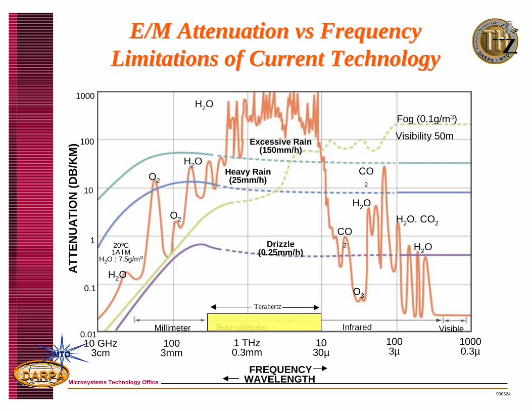
E/M Attenuation vs FrequencyE/M Attenuation vs FrequencyLimitations of Current TechnologyLimitations of Current Technology
AT
TE
NU
AT
ION
(D
B/K
M)
1000
100
10
1
0.01
0.1
10 GHz3cm
1003mm
1030µ
1 THz0.3mm
1003µ
10000.3µ
SubmillimeterMillimeter Infrared Visible
FREQUENCYWAVELENGTH
H2O
H2O
O2
CO2
O2CO
2
O3
H2O
H2O. CO2
H2O
Heavy Rain(25mm/h)
Drizzle(0.25mm/h)
H2O
20oC1ATM
H2O : 7.5g/m3
Visibility 50m
Fog (0.1g/m3)
Excessive Rain(150mm/h)
Terahertz

990624
DARPADARPAMicrosystems Technology Office
MTOMTO
Using a limitation to our advantage!!!Using a limitation to our advantage!!!
990624
DARPADARPAMicrosystems Technology Office
MTOMTO
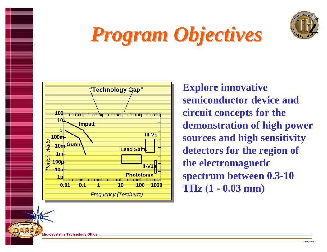
Program ObjectivesProgram Objectives
Explore innovative semiconductor device and circuit concepts for the demonstration of high power sources and high sensitivity detectors for the region of the electromagnetic spectrum between 0.3-10 THz (1 - 0.03 mm)
Frequency (Terahertz)
Pow
er, W
atts
“Technology Gap”
Lead Salts
III-Vs
II-V1s
Phototonic
0.01 0.1 1 10 100 1000
Impatt
Gunn
10010
1100m
10m
1m
100µ
10µ1µ
990624
DARPADARPAMicrosystems Technology Office
MTOMTO
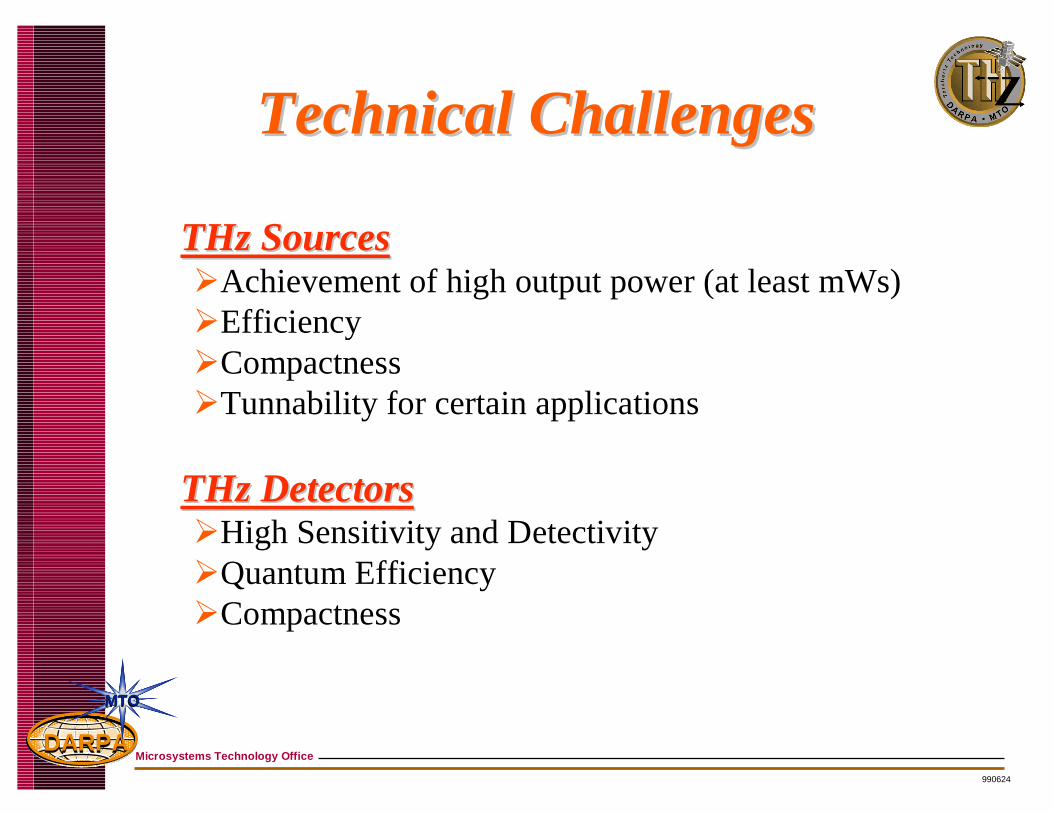
Technical ChallengesTechnical Challenges
THz SourcesTHz Sources�Achievement of high output power (at least mWs)�Efficiency�Compactness�Tunnability for certain applications
THz DetectorsTHz Detectors�High Sensitivity and Detectivity�Quantum Efficiency�Compactness

990624
DARPADARPAMicrosystems Technology Office
MTOMTO
• InP-and Sb-based HEMTs
• GaN-based Gunn diodes
• Sb-based Stark Ladders and Quasi-optic Combiners
• Passives and Wave-guides
• Optical Photomixing
• SiGe VCSELs
THz DetectorsTHz Sources
Technical ApproachesTechnical Approaches
5D\WKHRQ�6\VWHPV�&RPSDQ\
ElectricalElectrical OpticalOptical • RTD-based
• Electro-acoustic Detectors (HEMTs)
• Photon assisted tunneling in QWs
• RTD-based
• Electro-acoustic Detectors (HEMTs)
• Photon assisted tunneling in QWs

990624
DARPADARPAMicrosystems Technology Office
MTOMTO
APPROACH:• Develop high performance HEMTMMIC sources with integrated antennasfor 0.3 THz to 1 THz frequency range
• Develop novel superlattice oscillatorsand multipliers for 1 THz to 10 THz frequency range
OBJECTIVE:Develop monolithic integrated circuits capable to generate power at 0.33 THz, 0.66 THz, 1 THz and 3 THz.
APPLICATIONS:•Remote sensing•High resolution imaging•High data-rate space communication
State of the art HEMT MMIC
Quantum Device Technologies for Quantum Device Technologies for THz Communications and ImagingTHz Communications and Imaging
Quasi-optical superlattice array for harmonic generation
990624
DARPADARPAMicrosystems Technology Office
MTOMTO
0.3 THz to 1 THz SOURCES0.3 THz to 1 THz SOURCES
X2
Oscillator Amplifier ActiveDoubler
Amplifier Antenna
165 GHz 165 GHz 0.33 THz 0.33 THz 0.33 THz
X2
Oscillator Amplifier ActiveDoubler
Amplifier
165 GHz 165 GHz 0.33 THz 0.33 THz
Amplifier
0.33 THz
X3
ActiveTripler
X3
1 THz
Antenna
1 THz
CHALLENGES• MMIC design
• Low-loss passive components– Antennas
– Transmission lines– Power combiners
• Spatial power combining• Packaging
• Testing
CHALLENGES• MMIC design
• Low-loss passive components– Antennas
– Transmission lines– Power combiners
• Spatial power combining• Packaging
• Testing

990624
DARPADARPAMicrosystems Technology Office
MTOMTO
InAsInAs//AlSbAlSb//GaSbGaSbMaterials EffortMaterials Effort
HEMT MMIC
1 THz
x 3
3 THz(1-10 THz)
SuperlatticeHarmonicGenerator
Antenna
3 THz
Quasi-optical superlattice arrayfor harmonic generation
• 1-10 THz source development
- collaboration with UCSB (Allen)
- InAs/AlSb superlattice devices
- emphasis on harmonic generation
• Materials support for Raytheon (Frazier)
- RTD structures
- High Jp
- IMSC MBE Capability
• 1-10 THz source development
- collaboration with UCSB (Allen)
- InAs/AlSb superlattice devices
- emphasis on harmonic generation
• Materials support for Raytheon (Frazier)
- RTD structures
- High Jp
- IMSC MBE Capability
990624
DARPADARPAMicrosystems Technology Office
MTOMTO
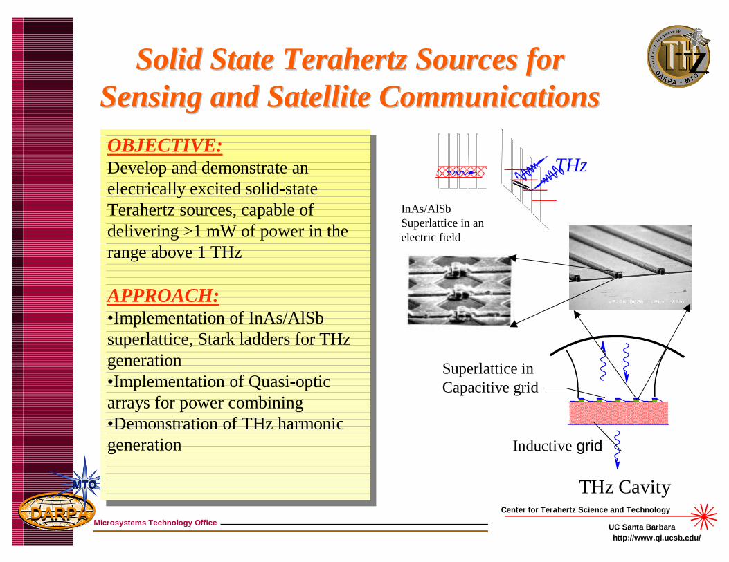
OBJECTIVE:Develop and demonstrate an electrically excited solid-state Terahertz sources, capable of delivering >1 mW of power in the range above 1 THz
APPROACH:•Implementation of InAs/AlSb superlattice, Stark ladders for THz generation•Implementation of Quasi-optic arrays for power combining•Demonstration of THz harmonic generation
Solid State Terahertz Sources for Solid State Terahertz Sources for Sensing and Satellite CommunicationsSensing and Satellite Communications
THz
InAs/AlSbSuperlattice in an electric field
THz Cavity
Inductive grid
Superlattice inCapacitive grid
Center for Terahertz Science and Technology
UC Santa Barbarahttp://www.qi.ucsb.edu/

990624
DARPADARPAMicrosystems Technology Office
MTOMTO
SolidSolid--State Terahertz Sources State Terahertz Sources
TECHNICAL APPROACH:
• Unique approach combining new semiconductor and micromachined concepts
• Semiconductor device potential for high-power fundamental or harmonic sources
• Possibility to apply micromachined concept to other sources developed under this program
TECHNICAL APPROACH:
• Unique approach combining new semiconductor and micromachined concepts
• Semiconductor device potential for high-power fundamental or harmonic sources
• Possibility to apply micromachined concept to other sources developed under this program
+ =× nGaN NDR Diodesfor THz signal Generation
Micromachined Resonator; Filter/Multiplier
Solid-State Terahertz Source
990624
DARPADARPAMicrosystems Technology Office
MTOMTO
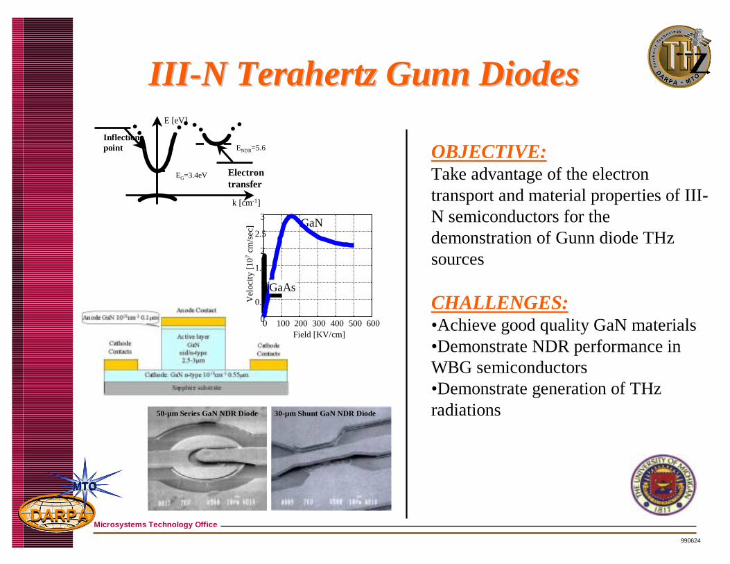
E [eV]
k [cm-1]
EG=3.4eV
ENDR=5.6Inflection point
Electron transfer
50-µm Series GaN NDR Diode 30-µm Shunt GaN NDR Diode
OBJECTIVE:Take advantage of the electron transport and material properties of III-N semiconductors for the demonstration of Gunn diode THzsources
CHALLENGES:•Achieve good quality GaN materials •Demonstrate NDR performance in WBG semiconductors•Demonstrate generation of THzradiations
IIIIII--N TerahertzN Terahertz GunnGunn DiodesDiodes
600Field [KV/cm]
Vel
ocit
y [1
07cm
/sec
]
0 100 200 300 400 5000
0.5
1
1.5
2
2.5
3GaN
GaAs
990624
DARPADARPAMicrosystems Technology Office
MTOMTO
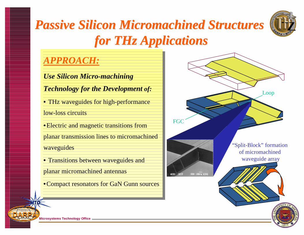
“Split-Block” formation of micromachinedwaveguide array
Loop
FGC
Passive Silicon Micromachined Structures Passive Silicon Micromachined Structures for THz Applicationsfor THz Applications
APPROACH:
Use Silicon Micro-machining
Technology for the Development of:
• THz waveguides for high-performance
low-loss circuits
•Electric and magnetic transitions from
planar transmission lines to micromachined
waveguides
• Transitions between waveguides and
planar micromachined antennas
•Compact resonators for GaN Gunn sources
990624
DARPADARPAMicrosystems Technology Office
MTOMTO
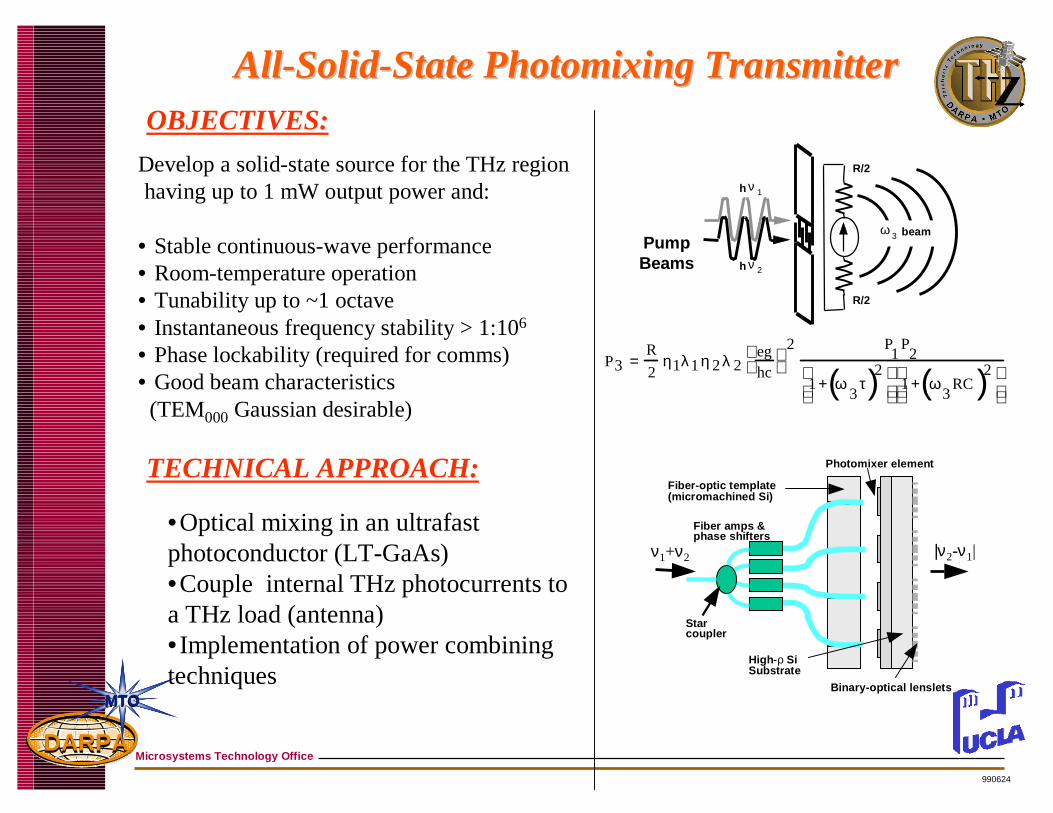
OBJECTIVES:
TECHNICAL APPROACH:
AllAll--SolidSolid--State Photomixing TransmitterState Photomixing Transmitter
Develop a solid-state source for the THz region having up to 1 mW output power and:
• Stable continuous-wave performance• Room-temperature operation• Tunability up to ~1 octave• Instantaneous frequency stability > 1:106
• Phase lockability (required for comms)• Good beam characteristics
(TEM000 Gaussian desirable)
•Optical mixing in an ultrafast photoconductor (LT-GaAs) •Couple internal THz photocurrents to a THz load (antenna)• Implementation of power combining techniques
ω 3 beamω 3 beam
h ν 1
h ν 2
R/2
R/2
PumpBeams
P3 =R
2η1λ1η 2λ 2
eghc
2 P1
P2
1+ ω3
τ( )2
1+ ω3
RC( )2
Photomixer element
High-ρ SiSubstrate
Fiber-optic template(micromachined Si)
ν1+ν2
Fiber amps &phase shifters
Starcoupler
|ν2-ν1|
Binary-optical lenslets

990624
DARPADARPAMicrosystems Technology Office
MTOMTO
OBJECTIVE:
To demonstrate a SiGe, micro-disk cavity, intersubband laser suitable for communication systems
APPROACH:
•Silicon micromachining for novel resonator design•SiGe unipolar architecture•E/M simulation for device optimization•1-10 THz operation
Quantum well transitions between E3 and E2. Proposed device will use SiGe quantum wells and hole intersubband transitions.
Pedestal
Si Substrate
WhisperingGalleryResonator
Active Layer
Radiation Radiation
Micro-disk lasers
THzTHz Sources Based onSources Based on IntersubbandIntersubbandTransitions inTransitions in SiGeSiGe Quantum WellsQuantum Wells
990624
DARPADARPAMicrosystems Technology Office
MTOMTO
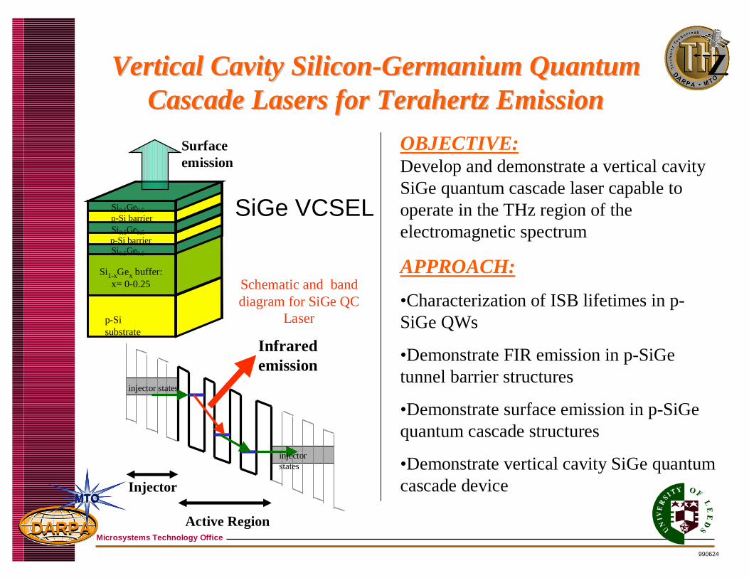
Vertical Cavity SiliconVertical Cavity Silicon--Germanium Quantum Germanium Quantum Cascade Lasers for Terahertz EmissionCascade Lasers for Terahertz Emission
OBJECTIVE:Develop and demonstrate a vertical cavitySiGe quantum cascade laser capable to operate in the THz region of the electromagnetic spectrum
APPROACH:
•Characterization of ISB lifetimes in p-SiGe QWs
•Demonstrate FIR emission in p-SiGetunnel barrier structures
•Demonstrate surface emission in p-SiGequantum cascade structures
•Demonstrate vertical cavity SiGe quantum cascade device
injector states
injector states
Active Region
Injector
Infrared emission
Schematic and band diagram for SiGe QC
Laser
SiGe VCSEL
p-Sisubstrate
Si1-xGex buffer: x= 0-0.25
Si0.5Ge0.5
Si0.5Ge0.5
Si0.5Ge0.5
p-Si barrier
p-Si barrier
Surface emission
990624
DARPADARPAMicrosystems Technology Office
MTOMTO
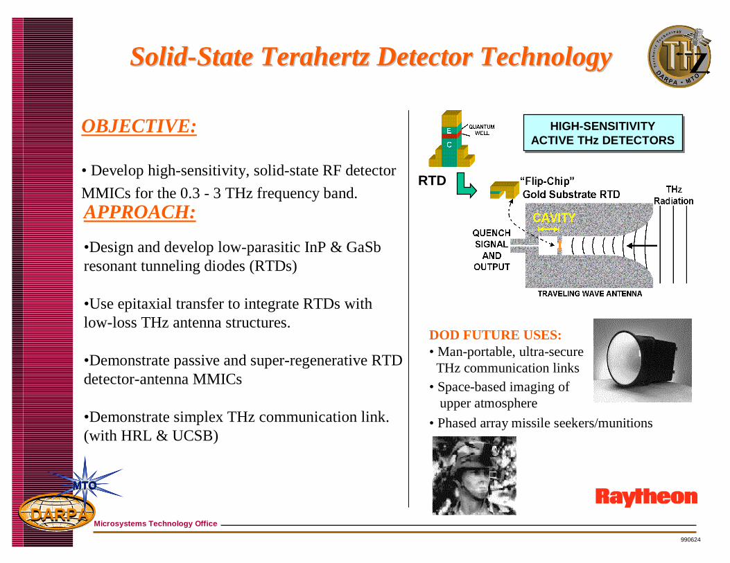
OBJECTIVE:
• Develop high-sensitivity, solid-state RF detector
MMICs for the 0.3 - 3 THz frequency band.
DOD FUTURE USES:• Man-portable, ultra-secure
THz communication links• Space-based imaging of
upper atmosphere
• Phased array missile seekers/munitions
SolidSolid--State Terahertz Detector TechnologyState Terahertz Detector Technology
APPROACH:
•Design and develop low-parasitic InP & GaSb resonant tunneling diodes (RTDs)
•Use epitaxial transfer to integrate RTDs with low-loss THz antenna structures.
•Demonstrate passive and super-regenerative RTD detector-antenna MMICs
•Demonstrate simplex THz communication link.(with HRL & UCSB)
HIGH-SENSITIVITYACTIVE THz DETECTORS
HIGH-SENSITIVITYACTIVE THz DETECTORS
RTD
990624
DARPADARPAMicrosystems Technology Office
MTOMTO
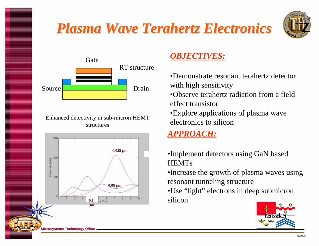
Plasma Wave Terahertz ElectronicsPlasma Wave Terahertz Electronics
OBJECTIVES:
•Demonstrate resonant terahertz detector with high sensitivity•Observe terahertz radiation from a field effect transistor•Explore applications of plasma wave electronics to silicon
APPROACH:
•Implement detectors using GaN based HEMTs•Increase the growth of plasma waves using resonant tunneling structure•Use “light” electrons in deep submicron silicon
Source Drain
GateRT structure
0.05 µm
0.1 µm
Enhanced detectivity in sub-micron HEMT structures
0.025 µm
990624
DARPADARPAMicrosystems Technology Office
MTOMTO
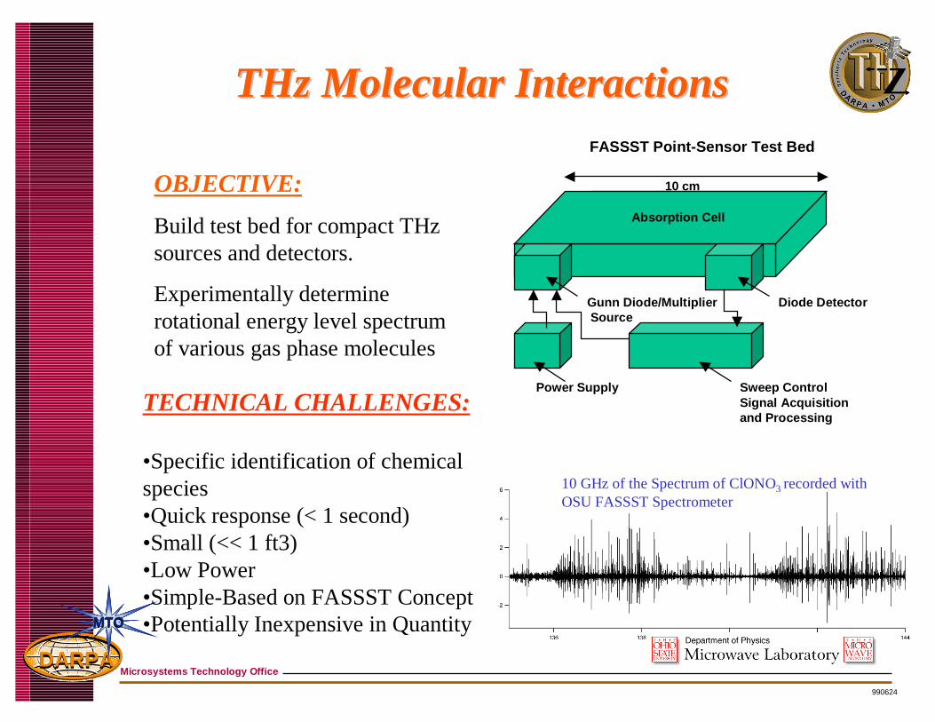
THz Molecular InteractionsTHz Molecular Interactions
TECHNICAL CHALLENGES:
•Specific identification of chemical species•Quick response (< 1 second)•Small (<< 1 ft3)•Low Power•Simple-Based on FASSST Concept•Potentially Inexpensive in Quantity
OBJECTIVE:
Build test bed for compact THz sources and detectors.
Experimentally determine rotational energy level spectrum of various gas phase molecules
Absorption Cell
Gunn Diode/MultiplierSource
Diode Detector
Power Supply Sweep ControlSignal Acquisitionand Processing
10 cm
FASSST Point-Sensor Test Bed
10 GHz of the Spectrum of ClONO3 recorded with OSU FASSST Spectrometer

990624
DARPADARPAMicrosystems Technology Office
MTOMTO
top QWcontact(source)
control gate
topdepletiongate
bottomQW
contact(drain)
bottom QW
top QWtunneling
back depletiongate
< 2 µm
quantized2D electronlayers
THz radiation
Double quantum well THz detector
concept
back control gate
top control gate
backdepletiongate
backdepletion
gate
2DEGcontact
2DEGcontact
topdepletion
gate
topdepletion
gate
Several bowtie DQW detectors have been fabricated
back control gate
top control gate
backdepletiongate
backdepletion
gate
2DEGcontact
2DEGcontact
topdepletion
gate
topdepletion
gate
Several bowtie DQW detectors have been fabricated
THz Detection Based on PhotonTHz Detection Based on Photon--assisted assisted Tunneling on Double Quantum WellsTunneling on Double Quantum Wells
kx
ky
EeVSD
µ1
µ2
photon∆E0occupiedstates
inhighdensityQW
unoccupiedstatesinlowdensityQW
photon
photonOBJECTIVE:
Demonstrate tunable, narrowband photon-assisted tunneling in double quantum well (DQW) heterostructures.
TECHNICAL APPROACH:
• Use bandgap engineering to optimize photodetectorperformance.
• Develop antenna structure compatible with THz detectors
• Bench-demonstration of THz detector system

990624
DARPADARPAMicrosystems Technology Office
MTOMTO
SummarySummary
• Environmental sensing
• Upper-atmosphere imagery
• Covert satellite communications
• Chem/Bio Detection (Near Distance)
DARPA is Creating Future Opportunities DARPA is Creating Future Opportunities forfor THzTHz Technology in:Technology in:
Related Documents