Darshan Hallur. International Journal of Engineering Research and Applications www.ijera.com ISSN: 2248-9622, Vol. 10, Issue 8, (Series-III) August 2020, pp. 29-52 www.ijera.com DOI: 10.9790/9622-1008032952 29 | Page New Switch Ladder Modified H-Bridge Multilevel Inverter with Sinusoidal Pulse Width Modulation Approach Darshan Hallur University: Bellary Institute of Technology and Management, Ballari. Designation: M. Tech in Power Electronic ABSTRACT For smaller switching losses, to reduce the strain on switches, with less PE devices, higher level of yield voltage, the systematic conversion of DC to AC is difficult task. To overcome all the above issues, changes made in recently developed bridge multilevel inverter set up, a new switch ladder modified multilevel inverter with sinusoidal PWM approach is introduced which reduces higher voltage rating on switches and also it helps to improve the switching order. This topology is differentiated with other preceding topology to convey the adequacy. --------------------------------------------------------------------------------------------------------------------------------------- Date of Submission: 06-08-2020 Date of Acceptance: 20-08-2020 --------------------------------------------------------------------------------------------------------------------------------------- I. INTRODUCTION 1.1 Introduction of multilevel inverter For transformation of DC to AC in commercial enterprise & sustainable force utilization, in a recent decade staggered MLI take part in basic ability.It can deliver yield voltage within the kind of steps, which covers and near sinusoidal waveform. In this manner, MLIs are viewed as higher in assessment with level inverters in expressions of makes use of. High efficiency and little quantity of preferred symphonious twisting (THD) are the big boundaries for the makes use of MLI. Different geographies of MLIs had been found within the previous no longer many decades. The main aim of MLI era is to produce well organised topography with little wide assortment of power introduce materials, with more number of yield voltage levels. As we go for higher voltage level with low operating branches, then the filter required at the yield can diminishes radically.By and large, MLIs are separated into three principal sorts which incorporates flying capacitors, diode clipped, and fell H-connect MLIs.In any case, all those everyday geologies have a couple of drawbacks, for instance, an increasingly important quantity of intensity electronic elements, condensers & DC supply. These elements create customary topographies ridiculous. MLI has different classifications. These are depending on DC potential sources, such as symmetric and asymmetric. Likewise, same degree of DC potential belonging named symmetric & with unequal DC potential size named as asymmetric. One of low frequency inverter is stairwell (SC). In this all operating branches operates at low frequency signal. This produces more losses due to signified grouping of electronic elements. Modified H- interface MLI as presented to direct the difficulty of symmetric and disproportionate complexities of DC assets, a currently out of the case new form is made. In any case, it solidifies of innumerable fragments and DC property whilst differentiated.To diminish the price, voltage pressure on operating branch setbacks, an immaculate symmetric topography of MLI is advanced in. This topography uses kinds of switches which include low repeat and high voltage circulate and severe repeat and unintentional voltage move. In any case, this topography has conflicting voltage scattering every unmarried through it branches. These drawbacks oppose it for excessive vlg programs.Further new geology of MLI is offered wherein has improved shape concerning variety of parts. Nevertheless, this topography has critical issue in it supervise method thinking about the lack of identity. For estimation of yield voltages, in these days out of the plastic new form is made based definitely at the chance of crossbreed MLI. Oppositely, this topography has a gigantic extensive kind of pressure electronic parts which makes it steadily conspicuous jumbled andunsuitable because of all the additionally buying and selling adversities. The operating method for device for PWM performs key limit in the presentation of new MLI. Distinctive operating procedures are superior. Additionally, MLIs solidifying small trading repeat method give practically all things taken into consideration execution appeared otherwise in terms RESEARCH ARTICLE OPEN ACCESS

Welcome message from author
This document is posted to help you gain knowledge. Please leave a comment to let me know what you think about it! Share it to your friends and learn new things together.
Transcript
Darshan Hallur. International Journal of Engineering Research and Applications
www.ijera.com
ISSN: 2248-9622, Vol. 10, Issue 8, (Series-III) August 2020, pp. 29-52
www.ijera.com DOI: 10.9790/9622-1008032952 29 | P a g e
New Switch Ladder Modified H-Bridge Multilevel Inverter with
Sinusoidal Pulse Width Modulation Approach
Darshan Hallur University: Bellary Institute of Technology and Management, Ballari.
Designation: M. Tech in Power Electronic
ABSTRACT For smaller switching losses, to reduce the strain on switches, with less PE devices, higher level of yield
voltage, the systematic conversion of DC to AC is difficult task. To overcome all the above issues, changes
made in recently developed bridge multilevel inverter set up, a new switch ladder modified multilevel inverter
with sinusoidal PWM approach is introduced which reduces higher voltage rating on switches and also it helps
to improve the switching order. This topology is differentiated with other preceding topology to convey the
adequacy.
----------------------------------------------------------------------------------------------------------------------------- ----------
Date of Submission: 06-08-2020 Date of Acceptance: 20-08-2020
----------------------------------------------------------------------------------------------------------------------------- ----------
I. INTRODUCTION 1.1 Introduction of multilevel inverter
For transformation of DC to AC in
commercial enterprise & sustainable force
utilization, in a recent decade staggered MLI take
part in basic ability.It can deliver yield voltage
within the kind of steps, which covers and near
sinusoidal waveform. In this manner, MLIs are
viewed as higher in assessment with level inverters
in expressions of makes use of. High efficiency and
little quantity of preferred symphonious twisting
(THD) are the big boundaries for the makes use of
MLI. Different geographies of MLIs had been found
within the previous no longer many decades. The
main aim of MLI era is to produce well organised
topography with little wide assortment of power
introduce materials, with more number of yield
voltage levels. As we go for higher voltage level
with low operating branches, then the filter required
at the yield can diminishes radically.By and large,
MLIs are separated into three principal sorts which
incorporates flying capacitors, diode clipped, and
fell H-connect MLIs.In any case, all those everyday
geologies have a couple of drawbacks, for instance,
an increasingly important quantity of intensity
electronic elements, condensers & DC supply.
These elements create customary topographies
ridiculous.
MLI has different classifications. These are
depending on DC potential sources, such as
symmetric and asymmetric. Likewise, same degree
of DC potential belonging named symmetric & with
unequal DC potential size named as asymmetric.
One of low frequency inverter is stairwell (SC). In
this all operating branches operates at low frequency
signal. This produces more losses due to signified
grouping of electronic elements. Modified H-
interface MLI as presented to direct the difficulty of
symmetric and disproportionate complexities of DC
assets, a currently out of the case new form is made.
In any case, it solidifies of innumerable fragments
and DC property whilst differentiated.To diminish
the price, voltage pressure on operating branch
setbacks, an immaculate symmetric topography of
MLI is advanced in.
This topography uses kinds of switches
which include low repeat and high voltage circulate
and severe repeat and unintentional voltage move.
In any case, this topography has conflicting voltage
scattering every unmarried through it branches.
These drawbacks oppose it for excessive vlg
programs.Further new geology of MLI is offered
wherein has improved shape concerning variety of
parts. Nevertheless, this topography has critical
issue in it supervise method thinking about the lack
of identity. For estimation of yield voltages, in these
days out of the plastic new form is made based
definitely at the chance of crossbreed MLI.
Oppositely, this topography has a gigantic extensive
kind of pressure electronic parts which makes it
steadily conspicuous jumbled andunsuitable because
of all the additionally buying and selling adversities.
The operating method for device for PWM
performs key limit in the presentation of new MLI.
Distinctive operating procedures are superior.
Additionally, MLIs solidifying small trading repeat
method give practically all things taken into
consideration execution appeared otherwise in terms
RESEARCH ARTICLE OPEN ACCESS
Darshan Hallur. International Journal of Engineering Research and Applications
www.ijera.com
ISSN: 2248-9622, Vol. 10, Issue 8, (Series-III) August 2020, pp. 29-52
www.ijera.com DOI: 10.9790/9622-1008032952 30 | P a g e
of MLIs with excessive switching repeat strategies.
Although, transient response is enhancing, even it
operates at excessive operating repeat approach.
Distinctive excessive trading repeat method carries
SPWM, area vector PWM (SVPWM), degree
moved PWM (LSPWM) & section moved PWM
(PSPWM).SinwavePWM, in its miles without a
doubt no longer hard to actualize and it does now no
longer want any upgrade set of policies for
smoothed out Switching. Also, because of over the
pinnacle trading repeat, SPWM causes enormous
percentage of buying and selling hardships. In
SVPWM, the proportion of THD is significantly
much less.
Moreover, the trading progressions may be
managed and progressed. On the non-obligatory
hand, taking into consideration the gap vectors the
switching plan create to be dynamically
confounding and Clarke alternate is used for a
unique level application. LSPWM method is seen
because the supportive for the minimization of
THD. In addition, this procedure doesn’t have
befuddled shape. Moreover, if the capacitors are
accessible within the geology, the administer of
operating strategy amassing will come to be being
dynamically jumbled and it is impractical for flying
capacitor (FC) topography& fell H-interface (CHB)
topography. To alleviate current issues of LSPWM,
each exquisite method presented, this is called
asPSPWM. itis far instant to alter the geologies
inclusive of capacitors, this approach is right for FC
and CHB geology. But due to phase shifting
method, it generates large THD.Because of
difficulty and unsuitable, SHE, SVC & NLC
methods are not used, even these have low THD.
Though all of those methods withleast
measure of THD. Nevertheless, such methodologies
have gotten stunning and preposterous, at whatever
point used for a large diploma. In this project, to
cope with the troubles of maximum outrageous
voltage rating at the switches, kind of components,
share of THD, & measure of yield voltage levels, a
modified H-interface MLI is suggested in this
project. Additionally, operating branches within the
suggested geology are all through unidirectional. In
addition, a sinusoidal PWM method is moved, that
is used to propel the converting direction of
movement of the MLI to lessen the trading setbacks
and most noteworthy voltage pressure on the
operating branches.Also anded PWM method is
introduced, by this voltage proportions can alter as
per requirement.
1.2 Literature survey
Darshan Hallur. International Journal of Engineering Research and Applications
www.ijera.com
ISSN: 2248-9622, Vol. 10, Issue 8, (Series-III) August 2020, pp. 29-52
www.ijera.com DOI: 10.9790/9622-1008032952 31 | P a g e
1.3 Problem statement
To control the difficulty of maximum
excessive voltage range on switches, no. of parts,
measure of THD, and no. Of yield potential levels,
an altered H-connect MLI is proposed.
Switches utilized within the proposed
geography are commonly unidirectional.
Further, a sinusoidal PWM approach is
created, which is applied to enhance the
exchanging arrangement of MLI to restriction the
voltage weights on switches.
Also, for variant of yield voltage
significance, AND gate is used with PWM
technique, it is then combined with sinusoidal
PWM method.
The growth of AND pastime of regular
PWM signal isthat, it is easy to estimation of
inverter yield voltage.
Yield RMS worth can be differedby
converting commitment sample of PWM.
Alongside these traces it is simple to
synchronize the yield voltage with matrix a decent
approach to attach the inverter to the grid
II. EXISTING MULTILEVEL
INVERTERS AND PROPOSED MLI 2.1 Existing multilevel inverters
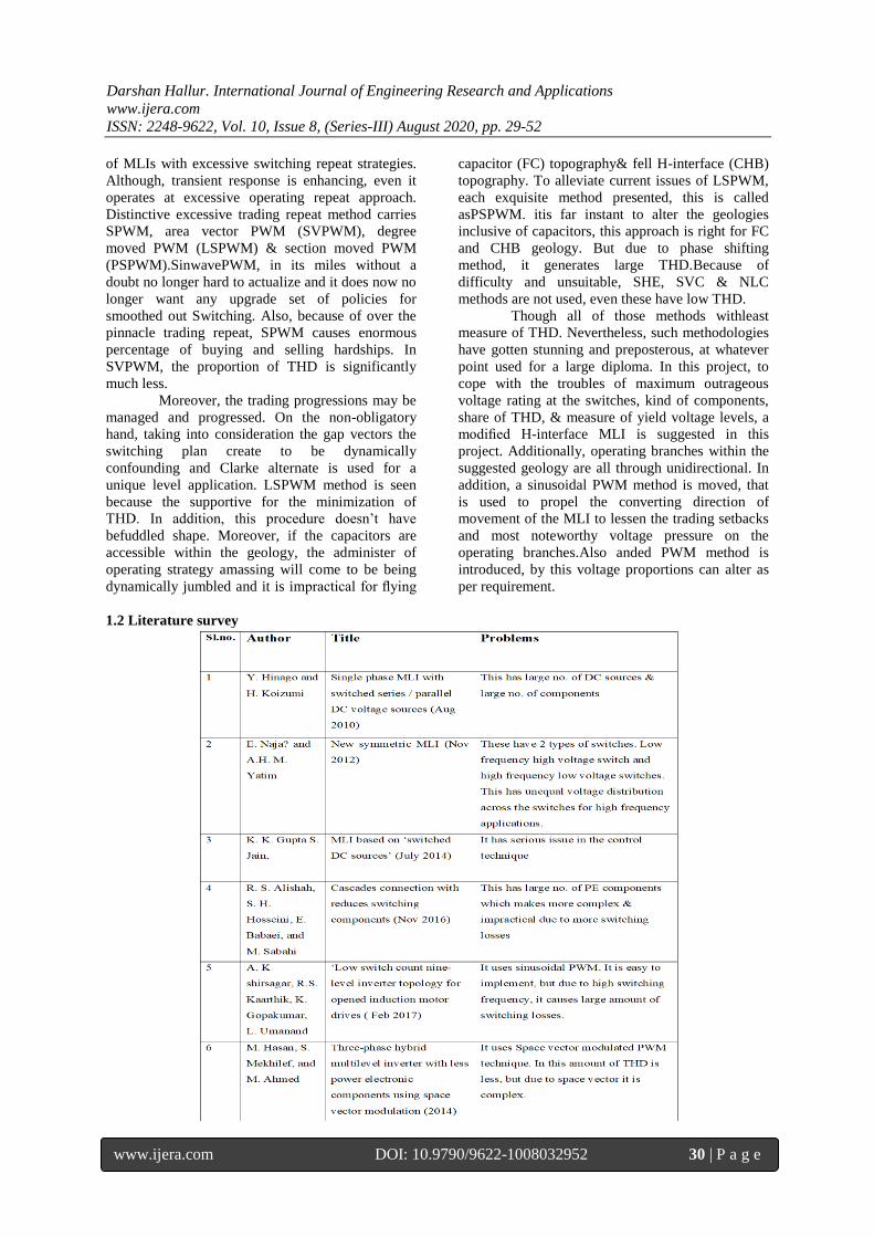
Figure 2.1back to back connected MLI
Above Figure 2.1 indicatesback to back connected
multilevel inverter.
Each basic cell has 4 switches
Each basic cell is called stage. Each stage
produces 3-levels output voltage.
For generation of 17-level output voltage
(n-1)/ 2 stages required. i.e. 32 switches are
required, 32 freewheeling diodes are required and 8
Dc voltage sources required.
Figure 2.2 switch ladder inverter
A recently developed new multi level inverter is
indicated in above Figure 2.2. It is modification of
cascaded H-bridge MLI
Here S1 and T1 switch is used, it can
conduct in two direction
It has six unidirectional switches. Hence
total 10 switches are required and 4 Dc sources are
required.
2.2 suggested switch ladder modified h-bridge
multilevelinverter
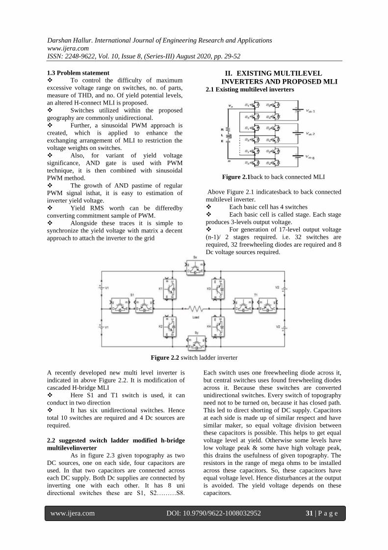
As in figure 2.3 given topography as two
DC sources, one on each side, four capacitors are
used. In that two capacitors are connected across
each DC supply. Both Dc supplies are connected by
inverting one with each other. It has 8 uni
directional switches these are S1, S2………S8.
Each switch uses one freewheeling diode across it,
but central switches uses found freewheeling diodes
across it. Because these switches are converted
unidirectional switches. Every switch of topography
need not to be turned on, because it has closed path.
This led to direct shorting of DC supply. Capacitors
at each side is made up of similar respect and have
similar maker, so equal voltage division between
these capacitors is possible. This helps to get equal
voltage level at yield. Otherwise some levels have
low voltage peak & some have high voltage peak,
this drains the usefulness of given topography. The
resistors in the range of mega ohms to be installed
across these capacitors. So, these capacitors have
equal voltage level. Hence disturbances at the output
is avoided. The yield voltage depends on these
capacitors.
Darshan Hallur. International Journal of Engineering Research and Applications
www.ijera.com
ISSN: 2248-9622, Vol. 10, Issue 8, (Series-III) August 2020, pp. 29-52
www.ijera.com DOI: 10.9790/9622-1008032952 32 | P a g e
FIGURE 2.3. SLMHBMLI circuit appearance
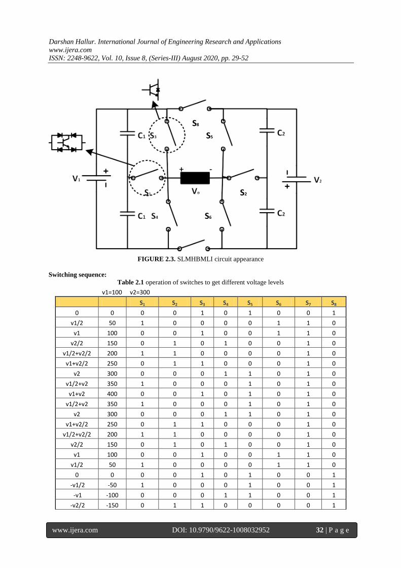
Switching sequence:
Table 2.1 operation of switches to get different voltage levels
v1=100 v2=300 S1 S2 S3 S4 S5 S6 S7 S8
0 0 0 0 1 0 1 0 0 1
v1/2 50 1 0 0 0 0 1 1 0
v1 100 0 0 1 0 0 1 1 0
v2/2 150 0 1 0 1 0 0 1 0
v1/2+v2/2 200 1 1 0 0 0 0 1 0
v1+v2/2 250 0 1 1 0 0 0 1 0
v2 300 0 0 0 1 1 0 1 0
v1/2+v2 350 1 0 0 0 1 0 1 0
v1+v2 400 0 0 1 0 1 0 1 0
v1/2+v2 350 1 0 0 0 1 0 1 0
v2 300 0 0 0 1 1 0 1 0
v1+v2/2 250 0 1 1 0 0 0 1 0
v1/2+v2/2 200 1 1 0 0 0 0 1 0
v2/2 150 0 1 0 1 0 0 1 0
v1 100 0 0 1 0 0 1 1 0
v1/2 50 1 0 0 0 0 1 1 0
0 0 0 0 1 0 1 0 0 1
-v1/2 -50 1 0 0 0 1 0 0 1
-v1 -100 0 0 0 1 1 0 0 1
-v2/2 -150 0 1 1 0 0 0 0 1
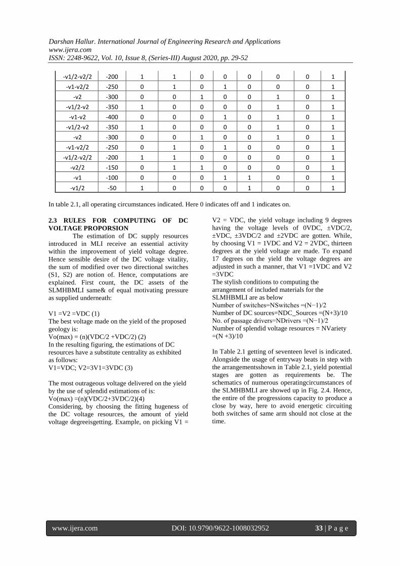
Darshan Hallur. International Journal of Engineering Research and Applications
www.ijera.com
ISSN: 2248-9622, Vol. 10, Issue 8, (Series-III) August 2020, pp. 29-52
www.ijera.com DOI: 10.9790/9622-1008032952 33 | P a g e
-v1/2-v2/2 -200 1 1 0 0 0 0 0 1
-v1-v2/2 -250 0 1 0 1 0 0 0 1
-v2 -300 0 0 1 0 0 1 0 1
-v1/2-v2 -350 1 0 0 0 0 1 0 1
-v1-v2 -400 0 0 0 1 0 1 0 1
-v1/2-v2 -350 1 0 0 0 0 1 0 1
-v2 -300 0 0 1 0 0 1 0 1
-v1-v2/2 -250 0 1 0 1 0 0 0 1
-v1/2-v2/2 -200 1 1 0 0 0 0 0 1
-v2/2 -150 0 1 1 0 0 0 0 1
-v1 -100 0 0 0 1 1 0 0 1
-v1/2 -50 1 0 0 0 1 0 0 1
In table 2.1, all operating circumstances indicated. Here 0 indicates off and 1 indicates on.
2.3 RULES FOR COMPUTING OF DC
VOLTAGE PROPORSION
The estimation of DC supply resources
introduced in MLI receive an essential activity
within the improvement of yield voltage degree.
Hence sensible desire of the DC voltage vitality,
the sum of modified over two directional switches
(S1, S2) are notion of. Hence, computations are
explained. First count, the DC assets of the
SLMHBMLI same& of equal motivating pressure
as supplied underneath:
V1 =V2 =VDC (1)
The best voltage made on the yield of the proposed
geology is:
Vo(max) = (n)(VDC/2 +VDC/2) (2)
In the resulting figuring, the estimations of DC
resources have a substitute centrality as exhibited
as follows:
V1=VDC; V2=3V1=3VDC (3)
The most outrageous voltage delivered on the yield
by the use of splendid estimations of is:
Vo(max) =(n)(VDC/2+3VDC/2)(4)
Considering, by choosing the fitting hugeness of
the DC voltage resources, the amount of yield
voltage degreeisgetting. Example, on picking V1 =
V2 = VDC, the yield voltage including 9 degrees
having the voltage levels of 0VDC, ±VDC/2,
±VDC, ±3VDC/2 and ±2VDC are gotten. While,
by choosing V1 = 1VDC and V2 = 2VDC, thirteen
degrees at the yield voltage are made. To expand
17 degrees on the yield the voltage degrees are
adjusted in such a manner, that V1 =1VDC and V2
=3VDC
The stylish conditions to computing the
arrangement of included materials for the
SLMHBMLI are as below
Number of switches=NSwitches =(N−1)/2
Number of DC sources=NDC_Sources =(N+3)/10
No. of passage drivers=NDrivers =(N−1)/2
Number of splendid voltage resources = NVariety
=(N +3)/10
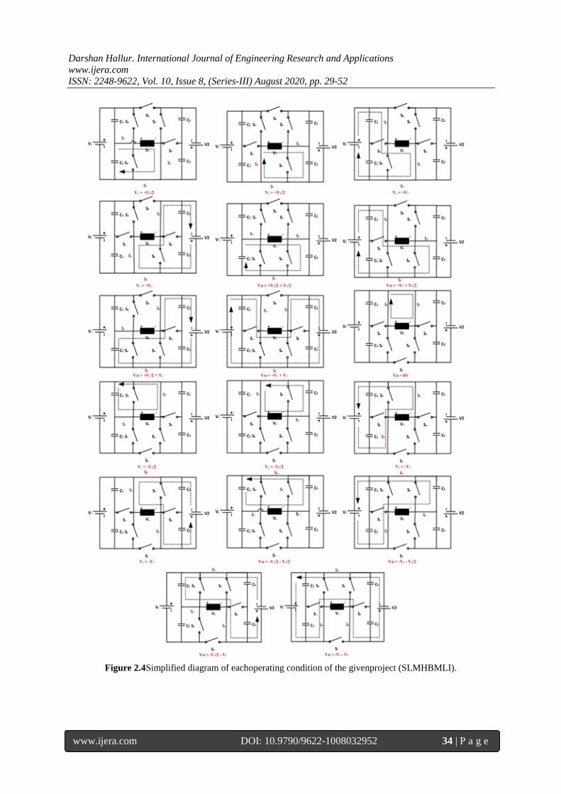
In Table 2.1 getting of seventeen level is indicated.
Alongside the usage of entryway beats in step with
the arrangementsshown in Table 2.1, yield potential
stages are gotten as requirements be. The
schematics of numerous operatingcircumstances of
the SLMHBMLI are showed up in Fig. 2.4. Hence,
the entire of the progressions capacity to produce a
close by way, here to avoid energetic circuiting
both switches of same arm should not close at the
time.
Darshan Hallur. International Journal of Engineering Research and Applications
www.ijera.com
ISSN: 2248-9622, Vol. 10, Issue 8, (Series-III) August 2020, pp. 29-52
www.ijera.com DOI: 10.9790/9622-1008032952 34 | P a g e
Figure 2.4Simplified diagram of eachoperating condition of the givenproject (SLMHBMLI).
Darshan Hallur. International Journal of Engineering Research and Applications
www.ijera.com
ISSN: 2248-9622, Vol. 10, Issue 8, (Series-III) August 2020, pp. 29-52
www.ijera.com DOI: 10.9790/9622-1008032952 35 | P a g e
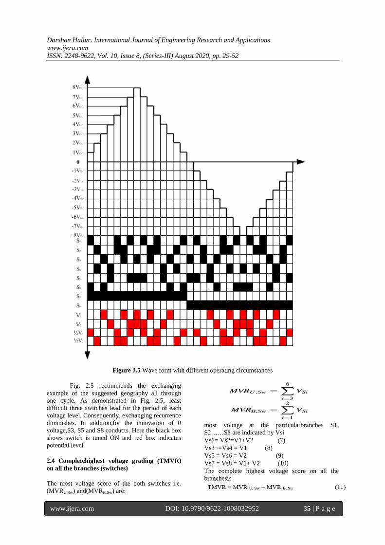
Figure 2.5 Wave form with different operating circumstances
Fig. 2.5 recommends the exchanging
example of the suggested geography all through
one cycle. As demonstrated in Fig. 2.5, least
difficult three switches lead for the period of each
voltage level. Consequently, exchanging recurrence
diminishes. In addition,for the innovation of 0
voltage,S3, S5 and S8 conducts. Here the black box
shows switch is tuned ON and red box indicates
potential level
2.4 Completehighest voltage grading (TMVR)
on all the branches (switches)
The most voltage score of the both switches i.e.
(MVRU.Sw) and(MVRB,Sw) are:
most voltage at the particularbranches S1,
S2……S8 are indicated by Vsi
Vs1= Vs2=V1+V2 (7)
Vs3¬=Vs4 = V1 (8)
Vs5 = Vs6 = V2 (9)
Vs7 = Vs8 = V1+ V2 (10)
The complete highest voltage score on all the
branchesis
Darshan Hallur. International Journal of Engineering Research and Applications
www.ijera.com
ISSN: 2248-9622, Vol. 10, Issue 8, (Series-III) August 2020, pp. 29-52
www.ijera.com DOI: 10.9790/9622-1008032952 36 | P a g e
Combining above equations,
TMVR = 6V1 + 6V2(12)
TMVR = 24V1 = 24VDC (13)
2.5 Losses occurrence in given topography
During MLI operation different losses
takes place. These are conduction and switching
incidents. During upward push even as the MLI is
in movement, conduction failure (Ploss, c)happens.
Due to present of branch controller like MOSFET,
diodes, these disasters happens. These are
delineated below
Pswitch (t) = [Vswitch+Rswitch I в (t)]* i(t) (14)
Pdiode (t) = [Vdiode+Rdiodei(t)]i(t) (15)
The potential drop across operating branches &
diodes are indicated by Vswitch and Vdiode.
Likewise, Rdiode&Rswitch are resistance of diode
and operating branch independently. Β addresses,
switch reliable. During the functioningof turning
ON & turning OFF of operating branches, the
operating adversities (Pswitching) happens. These
are delineated underneath.
Where, Vsw speaks to the Voltage at the transfer,
while it isn’t directing. Be that as it may, Ion and
Ioff speaks to the bleeding edge on the switch at
some point of and before its conduction
individually. The all-out misfortune (Ploss) of the
SLMHB-MLI will be:
Ploss = Ploss, c+Pswitching (20)
Ploss= (Pswitch (t)+Pdiode (t)) +(Ploss,
turn−on+Ploss,turn−off) (21)
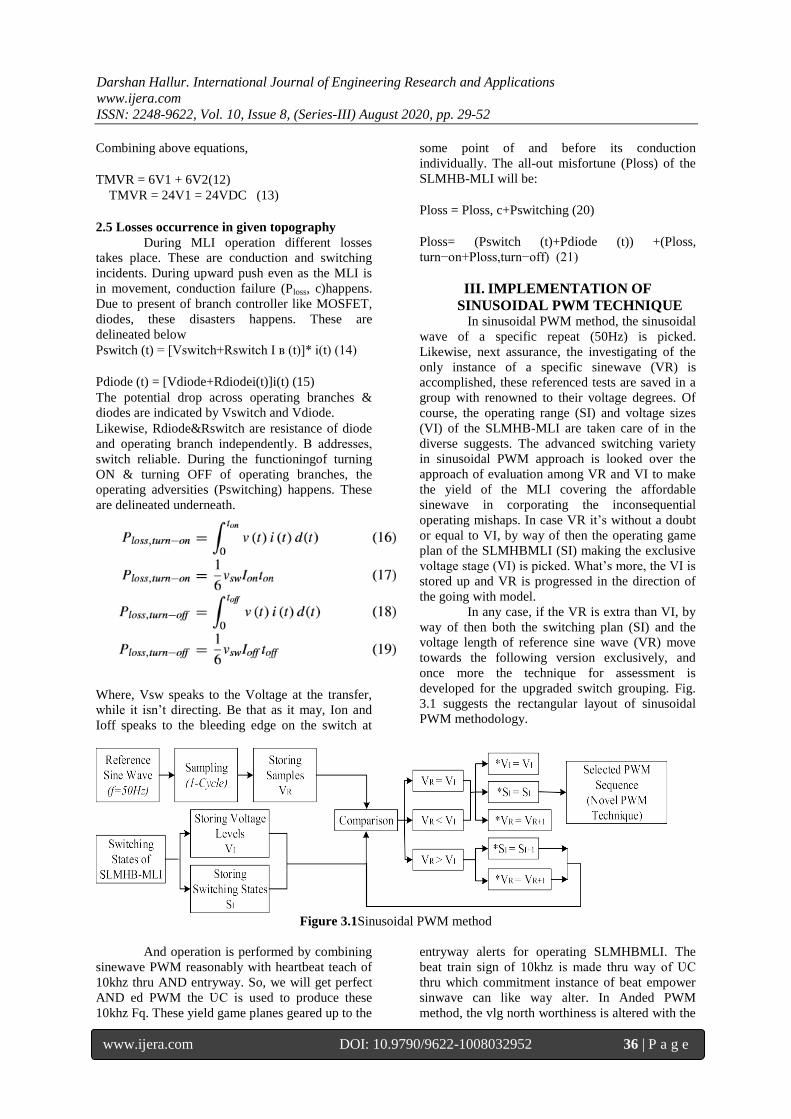
III. IMPLEMENTATION OF
SINUSOIDAL PWM TECHNIQUE In sinusoidal PWM method, the sinusoidal
wave of a specific repeat (50Hz) is picked.
Likewise, next assurance, the investigating of the
only instance of a specific sinewave (VR) is
accomplished, these referenced tests are saved in a
group with renowned to their voltage degrees. Of
course, the operating range (SI) and voltage sizes
(VI) of the SLMHB-MLI are taken care of in the
diverse suggests. The advanced switching variety
in sinusoidal PWM approach is looked over the
approach of evaluation among VR and VI to make
the yield of the MLI covering the affordable
sinewave in corporating the inconsequential
operating mishaps. In case VR it’s without a doubt
or equal to VI, by way of then the operating game
plan of the SLMHBMLI (SI) making the exclusive
voltage stage (VI) is picked. What’s more, the VI is
stored up and VR is progressed in the direction of
the going with model.
In any case, if the VR is extra than VI, by
way of then both the switching plan (SI) and the
voltage length of reference sine wave (VR) move
towards the following version exclusively, and
once more the technique for assessment is
developed for the upgraded switch grouping. Fig.
3.1 suggests the rectangular layout of sinusoidal
PWM methodology.
Figure 3.1Sinusoidal PWM method
And operation is performed by combining
sinewave PWM reasonably with heartbeat teach of
10khz thru AND entryway. So, we will get perfect
AND ed PWM the ƲC is used to produce these
10khz Fq. These yield game planes geared up to the
entryway alerts for operating SLMHBMLI. The
beat train sign of 10khz is made thru way of ƲC
thru which commitment instance of beat empower
sinwave can like way alter. In Anded PWM
method, the vlg north worthiness is altered with the
Darshan Hallur. International Journal of Engineering Research and Applications
www.ijera.com
ISSN: 2248-9622, Vol. 10, Issue 8, (Series-III) August 2020, pp. 29-52
www.ijera.com DOI: 10.9790/9622-1008032952 37 | P a g e
aid of strategies for converting the responsibility
instance of beat beat tech signal, in this manner, it
will in perfect to employ speed manipulate of
acknowledgement motor. This is shown in figure
3.2.
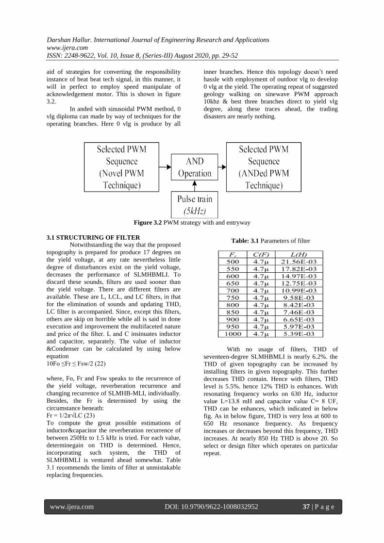
In anded with sinusoidal PWM method, 0
vlg diploma can made by way of techniques for the
operating branches. Here 0 vlg is produce by all
inner branches. Hence this topology doesn’t need
hassle with employment of outdoor vlg to develop
0 vlg at the yield. The operating repeat of suggested
geology walking on sinewave PWM approach
10khz & best three branches direct to yield vlg
degree, along these traces ahead, the trading
disasters are nearly nothing.
Figure 3.2 PWM strategy with and entryway
3.1 STRUCTURING OF FILTER
Notwithstanding the way that the proposed
topography is prepared for produce 17 degrees on
the yield voltage, at any rate nevertheless little
degree of disturbances exist on the yield voltage,
decreases the performance of SLMHBMLI. To
discard these sounds, filters are used sooner than
the yield voltage. There are different filters are
available. These are L, LCL, and LC filters, in that
for the elimination of sounds and updating THD,
LC filter is accompanied. Since, except this filters,
others are skip on horrible while all is said in done
execution and improvement the multifaceted nature
and price of the filter. L and C insinuates inductor
and capacitor, separately. The value of inductor
&Condenser can be calculated by using below
equation
10Fo ≤Fr ≤ Fsw/2 (22)
where, Fo, Fr and Fsw speaks to the recurrence of
the yield voltage, reverberation recurrence and
changing recurrence of SLMHB-MLI, individually.
Besides, the Fr is determined by using the
circumstance beneath:
Fr = 1/2π√LC (23)
To compute the great possible estimations of
inductor&capacitor the reverberation recurrence of
between 250Hz to 1.5 kHz is tried. For each value,
determinegain on THD is determined. Hence,
incorporating such system, the THD of
SLMHBMLI is ventured ahead somewhat. Table
3.1 recommends the limits of filter at unmistakable
replacing frequencies.
Table: 3.1 Parameters of filter
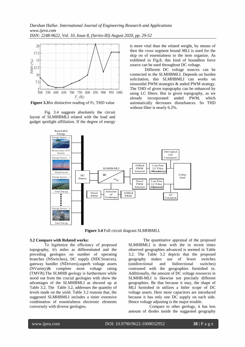
With no usage of filters, THD of
seventeen-degree SLMHBMLI is nearly 6.2%. the
THD of given topography can be increased by
installing filters in given topography. This further
decreases THD contain. Hence with filters, THD
level is 5.5%. hence 12% THD is enhances. With
resonating frequency works on 630 Hz, inductor
value L=13.8 mH and capacitor value C= 8 ƲF,
THD can be enhances, which indicated in below
fig. As in below figure, THD is very less at 600 to
650 Hz resonance frequency. As frequency
increases or decreases beyond this frequency, THD
increases. At nearly 850 Hz THD is above 20. So
select or design filter which operates on particular
repeat.
Darshan Hallur. International Journal of Engineering Research and Applications
www.ijera.com
ISSN: 2248-9622, Vol. 10, Issue 8, (Series-III) August 2020, pp. 29-52
www.ijera.com DOI: 10.9790/9622-1008032952 38 | P a g e
Figure 3.3for distinctive reading of Fr, THD value
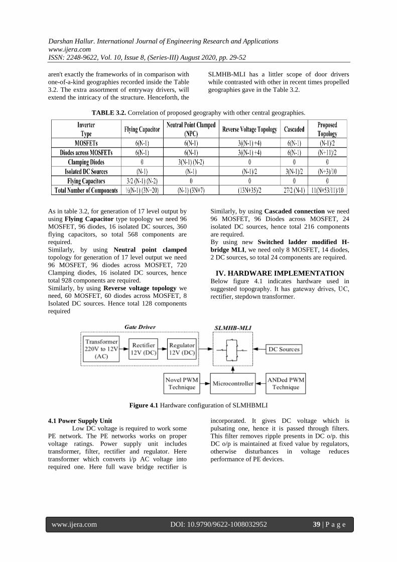
Fig. 3.4 suggests absolutely the circuit
layout of SLMHBMLI related with the load and
gadget spotlight affiliation. If the degree of energy
is more vital than the related weight, by means of
then the cross segment bound MLI is used for the
skip on of essentialness to the item organize. As
exhibited in Fig.8, this kind of boundless force
source can be used throughout DC voltage.
Different DC voltage sources can be
connected to the SLMHBMLI. Depends on burden
solicitation, this SLMHBMLI can works on
sinusoidal PWM strategies & anded PWM strategy.
The THD of given topography can be enhanced by
using LC filters. But in given topography, as we
already incorporated anded PWM, which
automatically decreases disturbances. So THD
without filter is nearly 6.2%.
Figure 3.4 Full circuit diagram SLMHBMLI.
3.2 Compare with Related works:
To legitimize the efficiency of proposed
topography, it's miles as differentiated and the
preceding geologies on number of operating
branches (NSwitches), DC supply (NDCSources),
gateway handler (NDrivers),superb voltage assets
(NVariety)& complete most voltage rating
(TMVR).The SLMHB geology is furthermore while
stood out from the crucial geologies with show the
advantages of the SLMHBMLI as showed up at
Table 3.2. The Table 3.2, addresses the quantity of
levels made on the yield. Table 3.2 reasons that, the
suggested SLMHBMLI includes a tinier extensive
combination of essentialness electronic elements
conversely with diverse geologies.
The quantitative appraisal of the proposed
SLMHBMLI is done with the in recent times
observed geographies advanced is seemed in Table
3.2. The Table 3.2 depicts that the proposed
geography makes use of fewer switches
(unidirectional and bidirectional switches)
contrasted with the geographies furnished in.
Additionally, the amount of DC voltage resources in
SLMHB-MLI is likewise not precisely different
geographies. Be that because it may, the shape of
MLI furnished in utilizes a littler scope of DC
voltage assets. Here more capacitors are introduced
because it has only one DC supply on each side.
Hence voltage adjusting is the major trouble.
Compare to other geology, it has less
amount of diodes inside the suggested geography
Darshan Hallur. International Journal of Engineering Research and Applications
www.ijera.com
ISSN: 2248-9622, Vol. 10, Issue 8, (Series-III) August 2020, pp. 29-52
www.ijera.com DOI: 10.9790/9622-1008032952 39 | P a g e
aren't exactly the frameworks of in comparison with
one-of-a-kind geographies recorded inside the Table
3.2. The extra assortment of entryway drivers, will
extend the intricacy of the structure. Henceforth, the
SLMHB-MLI has a littler scope of door drivers
while contrasted with other in recent times propelled
geographies gave in the Table 3.2.
TABLE 3.2. Correlation of proposed geography with other central geographies.
As in table 3.2, for generation of 17 level output by
using Flying Capacitor type topology we need 96
MOSFET, 96 diodes, 16 isolated DC sources, 360
flying capacitors, so total 568 components are
required.
Similarly, by using Neutral point clamped
topology for generation of 17 level output we need
96 MOSFET, 96 diodes across MOSFET, 720
Clamping diodes, 16 isolated DC sources, hence
total 928 components are required.
Similarly, by using Reverse voltage topology we
need, 60 MOSFET, 60 diodes across MOSFET, 8
Isolated DC sources. Hence total 128 components
required
Similarly, by using Cascaded connection we need
96 MOSFET, 96 Diodes across MOSFET, 24
isolated DC sources, hence total 216 components
are required.
By using new Switched ladder modified H-
bridge MLI, we need only 8 MOSFET, 14 diodes,
2 DC sources, so total 24 components are required.
IV. HARDWARE IMPLEMENTATION Below figure 4.1 indicates hardware used in
suggested topography. It has gateway drives, ƲC,
rectifier, stepdown transformer.
Figure 4.1 Hardware configuration of SLMHBMLI
4.1 Power Supply Unit
Low DC voltage is required to work some
PE network. The PE networks works on proper
voltage ratings. Power supply unit includes
transformer, filter, rectifier and regulator. Here
transformer which converts i/p AC voltage into
required one. Here full wave bridge rectifier is
incorporated. It gives DC voltage which is
pulsating one, hence it is passed through filters.
This filter removes ripple presents in DC o/p. this
DC o/p is maintained at fixed value by regulators,
otherwise disturbances in voltage reduces
performance of PE devices.
Darshan Hallur. International Journal of Engineering Research and Applications
www.ijera.com
ISSN: 2248-9622, Vol. 10, Issue 8, (Series-III) August 2020, pp. 29-52
www.ijera.com DOI: 10.9790/9622-1008032952 40 | P a g e
Figure 4.2Block diagram indicates flow of power
4.1.1 Transformer
A transformer is a static devicewhich
transforms electric first-rate in a single circuit is
moved into electric nature of same repeat in some
other circuit. The voltage enhancement or
educement cab be yield with this. It works on
faradays law.In my work, step down transformer is
used, which step downs the voltage to 12 V.
4.1.2 Rectifier
Rectifiers are used to convert AC to DC, because
some circuits work on DC. This rectifierhas diodes
for conversion. To get maximum DC level, we use
bridge rectifier. There are many different alterable
are available. These are IN4001, IN4003, IN4007
likewise. However, IN4007 is used considering the
way that could gaze upward to has great deal as
1000V.
In my work I have using DB107 and AN4007
diodes, which gives 12V output voltage. This
voltage is given to Voltage regulator after filtering
it.
Figure 4.3 DB107 bridge rectifier
Figure4.3 shows bridge rectifier. It is made by
Rectron semiconductor manufacturer. Its voltage
rating is 50V to 1000V, forward output current is 1
Amp. It can operate at -55 to +150-degree Celsius.
IN4007 Diode is used for driver circuit. It is
manufactured by Fairchild semiconductor. It has
less onward voltage drop, high peak withstandable
current capability. Its current rating s 1 Amp and
operates at -55 to +150 °C.
Figure 4.4 IN4007 diode
4.1.3 Filters
Filters are used to eliminate the content of AC from
DC. Here condenser is connected across rectifier
o/p. This capacitor passes AC and blocks DC, hence
we get pure DC o/p. this o/p has less ripple, so it can
be useful to connect for loads, hence disturbances
eliminated
4.1.4 Regulators
Here regulators are used to maintain constant vlg. It
does not change even of i/p vlg changes. Its o/p does
not alter if external variables like load, temperature
alter.
In my work, LM7805 vlg regulator is used. It is +5V
regulator. It is used for ƲC.
Figure 4.5 LM7805 Voltage regulator IC
Darshan Hallur. International Journal of Engineering Research and Applications
www.ijera.com
ISSN: 2248-9622, Vol. 10, Issue 8, (Series-III) August 2020, pp. 29-52
www.ijera.com DOI: 10.9790/9622-1008032952 41 | P a g e
LM78XX series is the 3-terminal regulator,
available in TO 220 modules. It gives a fixed o/p
voltage. It is useful in a wide range of applications.
Each type performs internal current limiting. It has
thermal shutdown and safe operating area
protection. It is unbreakable. By providing extra
heat sink, it can give 1A output current. It is
basically adapted a fixed voltage regulator.
LM7805is made by 3
pinsandthepindetailsareasfollow:
1: The rectified output voltage after filtering is
connected to this pin
2: this is ground pin. This makes ground
connection to regulator
3: this pin gives a 5V regulated DC supply to the
controller
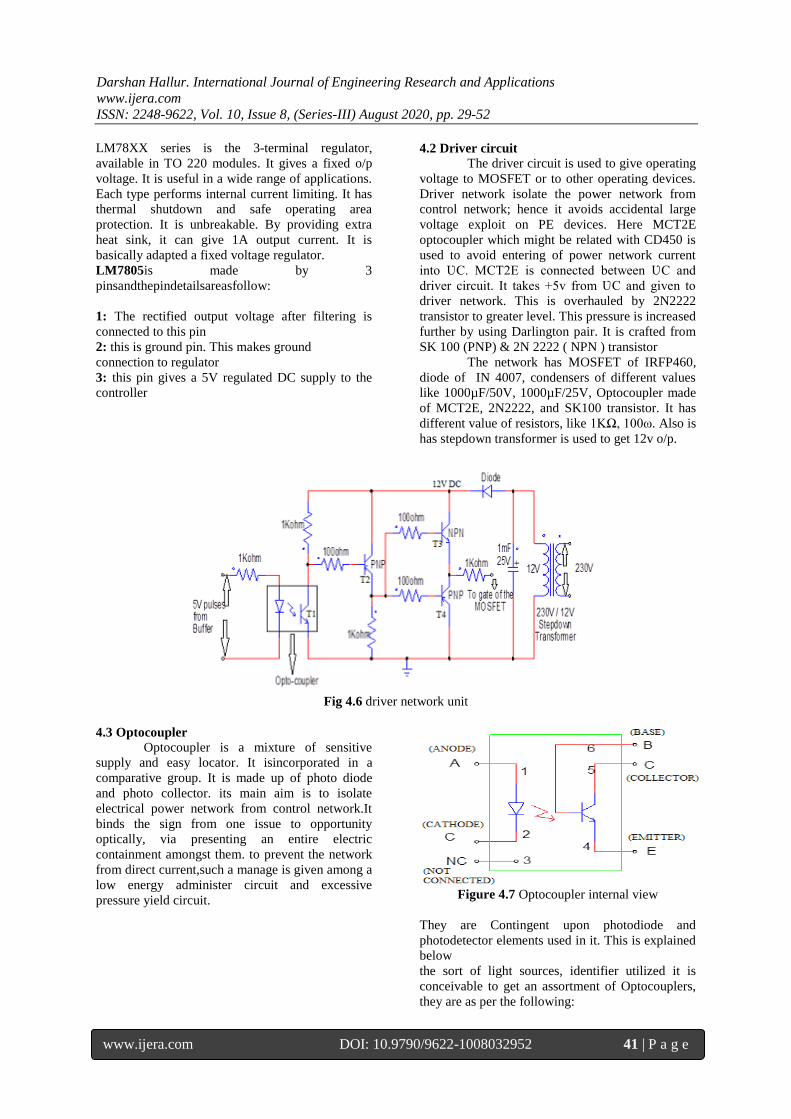
4.2 Driver circuit
The driver circuit is used to give operating
voltage to MOSFET or to other operating devices.
Driver network isolate the power network from
control network; hence it avoids accidental large
voltage exploit on PE devices. Here MCT2E
optocoupler which might be related with CD450 is
used to avoid entering of power network current
into ƲC. MCT2E is connected between ƲC and
driver circuit. It takes +5v from ƲC and given to
driver network. This is overhauled by 2N2222
transistor to greater level. This pressure is increased
further by using Darlington pair. It is crafted from
SK 100 (PNP) & 2N 2222 ( NPN ) transistor
The network has MOSFET of IRFP460,
diode of IN 4007, condensers of different values
like 1000µF/50V, 1000µF/25V, Optocoupler made
of MCT2E, 2N2222, and SK100 transistor. It has
different value of resistors, like 1KΩ, 100ω. Also is
has stepdown transformer is used to get 12v o/p.
Fig 4.6 driver network unit
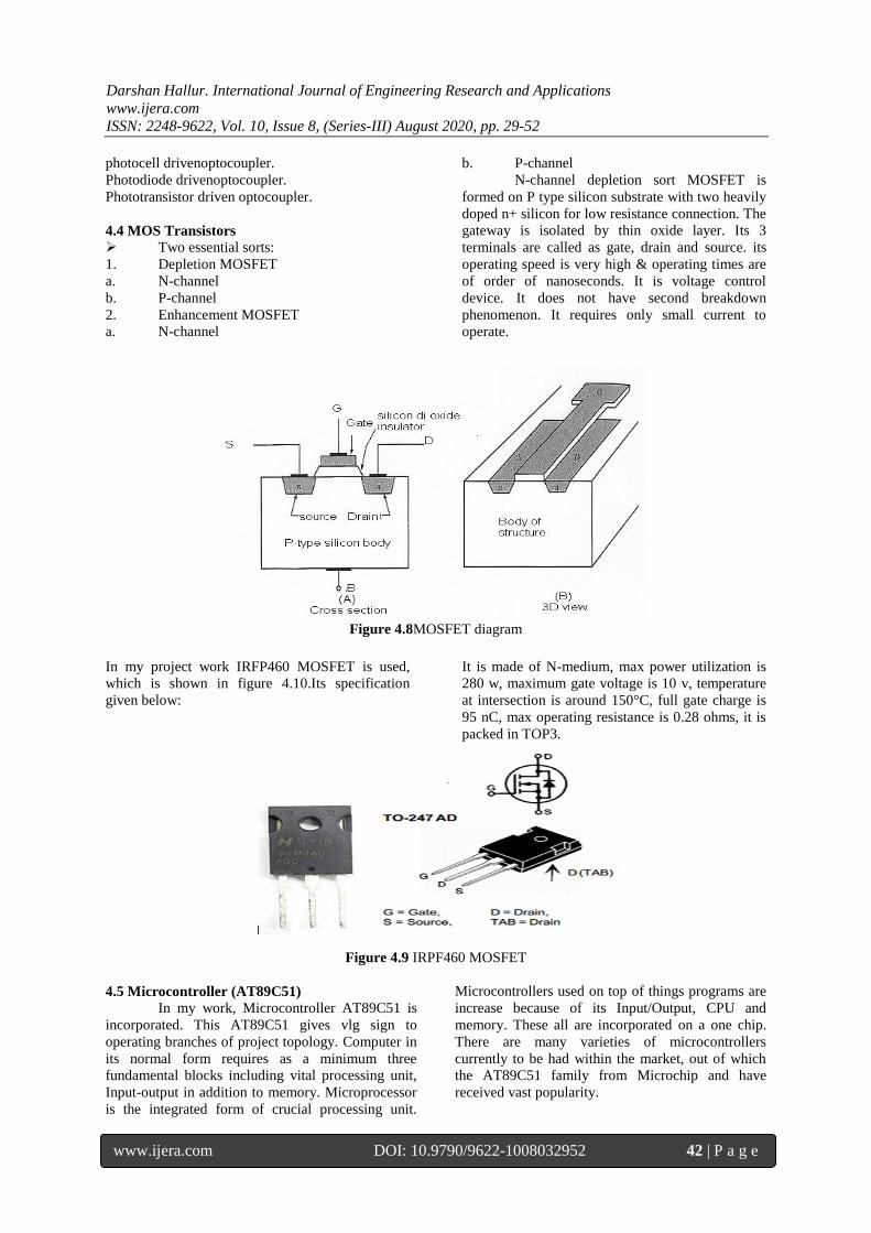
4.3 Optocoupler
Optocoupler is a mixture of sensitive
supply and easy locator. It isincorporated in a
comparative group. It is made up of photo diode
and photo collector. its main aim is to isolate
electrical power network from control network.It
binds the sign from one issue to opportunity
optically, via presenting an entire electric
containment amongst them. to prevent the network
from direct current,such a manage is given among a
low energy administer circuit and excessive
pressure yield circuit.
Figure 4.7 Optocoupler internal view
They are Contingent upon photodiode and
photodetector elements used in it. This is explained
below
the sort of light sources, identifier utilized it is
conceivable to get an assortment of Optocouplers,
they are as per the following:
Darshan Hallur. International Journal of Engineering Research and Applications
www.ijera.com
ISSN: 2248-9622, Vol. 10, Issue 8, (Series-III) August 2020, pp. 29-52
www.ijera.com DOI: 10.9790/9622-1008032952 42 | P a g e
photocell drivenoptocoupler.
Photodiode drivenoptocoupler.
Phototransistor driven optocoupler.
4.4 MOS Transistors
Two essential sorts:
1. Depletion MOSFET
a. N-channel
b. P-channel
2. Enhancement MOSFET
a. N-channel
b. P-channel
N-channel depletion sort MOSFET is
formed on P type silicon substrate with two heavily
doped n+ silicon for low resistance connection. The
gateway is isolated by thin oxide layer. Its 3
terminals are called as gate, drain and source. its
operating speed is very high & operating times are
of order of nanoseconds. It is voltage control
device. It does not have second breakdown
phenomenon. It requires only small current to
operate.
Figure 4.8MOSFET diagram
In my project work IRFP460 MOSFET is used,
which is shown in figure 4.10.Its specification
given below:
It is made of N-medium, max power utilization is
280 w, maximum gate voltage is 10 v, temperature
at intersection is around 150°C, full gate charge is
95 nC, max operating resistance is 0.28 ohms, it is
packed in TOP3.
Figure 4.9 IRPF460 MOSFET
4.5 Microcontroller (AT89C51)
In my work, Microcontroller AT89C51 is
incorporated. This AT89C51 gives vlg sign to
operating branches of project topology. Computer in
its normal form requires as a minimum three
fundamental blocks including vital processing unit,
Input-output in addition to memory. Microprocessor
is the integrated form of crucial processing unit.
Microcontrollers used on top of things programs are
increase because of its Input/Output, CPU and
memory. These all are incorporated on a one chip.
There are many varieties of microcontrollers
currently to be had within the market, out of which
the AT89C51 family from Microchip and have
received vast popularity.
Darshan Hallur. International Journal of Engineering Research and Applications
www.ijera.com
ISSN: 2248-9622, Vol. 10, Issue 8, (Series-III) August 2020, pp. 29-52
www.ijera.com DOI: 10.9790/9622-1008032952 43 | P a g e
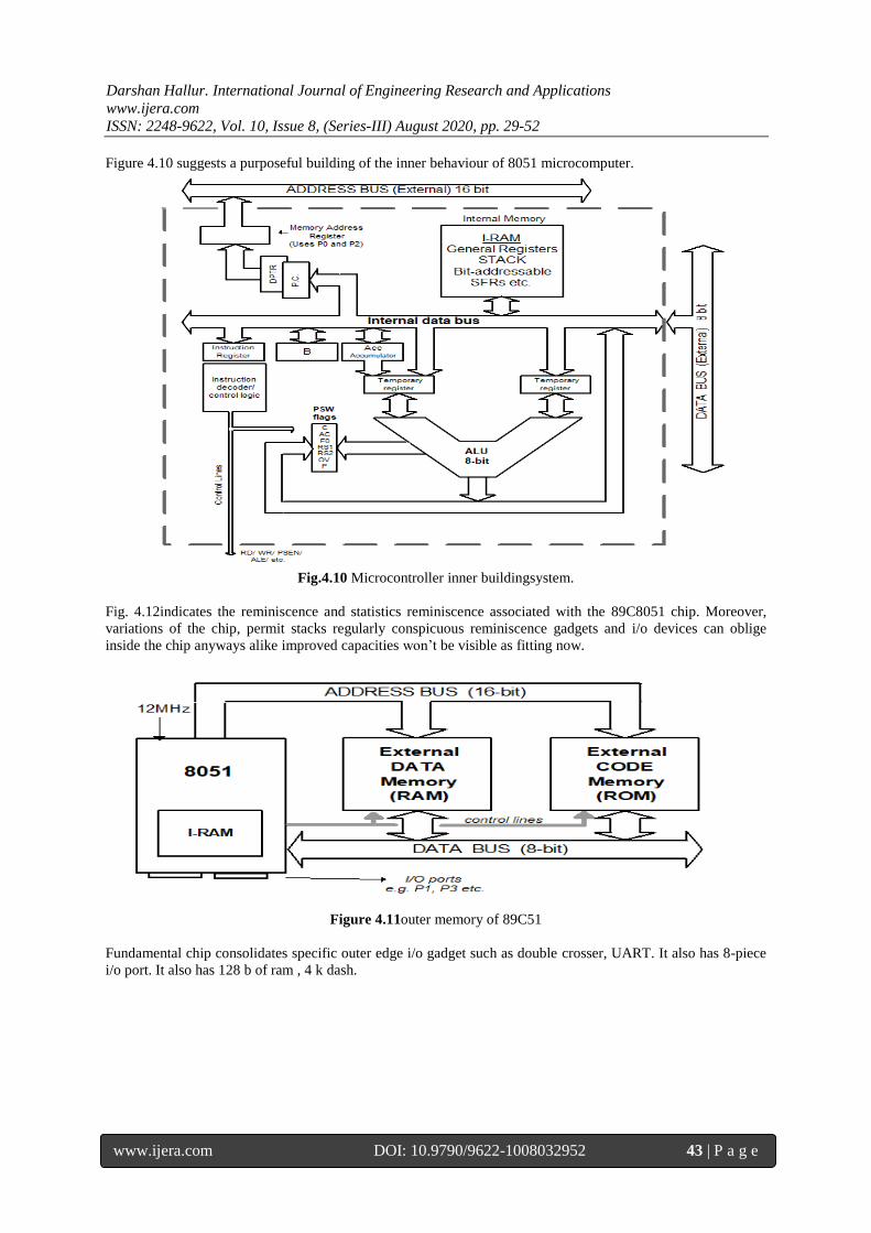
Figure 4.10 suggests a purposeful building of the inner behaviour of 8051 microcomputer.
Fig.4.10 Microcontroller inner buildingsystem.
Fig. 4.12indicates the reminiscence and statistics reminiscence associated with the 89C8051 chip. Moreover,
variations of the chip, permit stacks regularly conspicuous reminiscence gadgets and i/o devices can oblige
inside the chip anyways alike improved capacities won’t be visible as fitting now.
Figure 4.11outer memory of 89C51
Fundamental chip consolidates specific outer edge i/o gadget such as double crosser, UART. It also has 8-piece
i/o port. It also has 128 b of ram , 4 k dash.
Darshan Hallur. International Journal of Engineering Research and Applications
www.ijera.com
ISSN: 2248-9622, Vol. 10, Issue 8, (Series-III) August 2020, pp. 29-52
www.ijera.com DOI: 10.9790/9622-1008032952 44 | P a g e
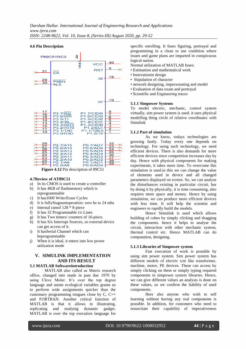
4.6 Pin Description
Figure 4.12 Pin description of 89C51
4.7Review of AT89C51
a) In its CMOS is used to create a controller
b) It has 4KB of flashmemory which is
reprogrammable
c) It has1000 Write/Erase Cycles
d) It is fullyStagnantoperation: zero hz to 24 mhz
e) Internal ramof 128 * 8-piece
f) It has 32 Programmable i/o Lines
g) It has Two timers/ counters of 16-piece.
h) It has Six Interrupt Sources, so external device
can get access of it.
i) It hasSerial Channel which can
beprogrammable
j) When it is ideal, it enters into low power
utilization mode
V. SIMULINK IMPLEMENTATION
AND ITS RESULT 5.1 MATLAB Softwareintroduction
MATLAB also called as Matrix research
office, changed into made in past due 1970 by
using Cleve Moler. It’s over the top degree
language and astute ecological variables grants us
to perform wide assignments quicker than the
customary programming tongues close by C, C++
and FORTRAN. Another critical function of
MATLAB is that it allows in illustrating,
replicating and studying dynamic gadget.
MATLAB is over the top execution language for
specific enrolling. It fuses figuring, portrayal and
programming in a clean to use condition where
issues and game plans are imparted in conspicuous
logical nation.
Normal utilization of MATLAB fuses:
• Estimation and mathematical work
• Innovationin design
• Stipulation of character
• network designing, impersonating and model
• Evaluation of data exam and portrayal
• Scientific and Engineering traces
5.1.1 Simpower Systems
To model electric, mechanic, control system
virtually, sim power system is used. it uses physical
modelling thing circle of relative coordinates with
Simulink
5.1.2 Part of simulation
As we know, todays technologies are
growing fastly. Today every one depends on
technology. For using such technology, we need
efficient devices. There is also demands for more
efficient devices since competition increases day by
day. Hence with physical components for making
experiments, it takes more time. To overcome this
simulation is used.in this we can change the value
of elements used in device and all changed
parameters displayed on screen. So, we can analyse
the disturbances existing in particular circuit, bur
by doing it by physically, it is time consuming, also
requires more space and money. Hence by using
simulation, we can produce more efficient devices
with less time. It will help the scientist and
engineers to rapidly build the models.
Hence Simulink is used which allows
building of cubes by simply clicking and dragging
the components. hence it helps to analyse the
circuit, interaction with other mechanic system,
thermal control etc. Hence MATLAB can do
computation, designing.
5.1.3 Libraries of Simpower system
Fast execution of work is possible by
using sim power system. Sim power system has
different models of electric s/m like transformer,
machine, motor, PE devices. These can access by
simply clicking on them or simply typing required
components in simpower system libraries. Hence,
we can give different values an analysis is done on
these values, so we confirm the liability of used
components.
Here also anyone who wish to self
learning without having any real components is
possible. In addition, for customers who need to
resuscitate their capability of imperativeness
Darshan Hallur. International Journal of Engineering Research and Applications
www.ijera.com
ISSN: 2248-9622, Vol. 10, Issue 8, (Series-III) August 2020, pp. 29-52
www.ijera.com DOI: 10.9790/9622-1008032952 45 | P a g e
system speculation, there moreover are self getting
progressively familiar with related examinations.
5.2 Sample circuit designing
As we already know by previous that sim power
system can be used to analyse linear and non linear
elements. For sample circuit designing follow the
following procedures
1. Open the power lib library of sim power
system
2. Get knowledge to build simple network
3. Connect your network to Simulink
Here we can discuss some topics:
1. By using power lib build electrical
2. Connection of electrical network with
Simulink
3. How to measure current and voltage
5.3 Electric network designing
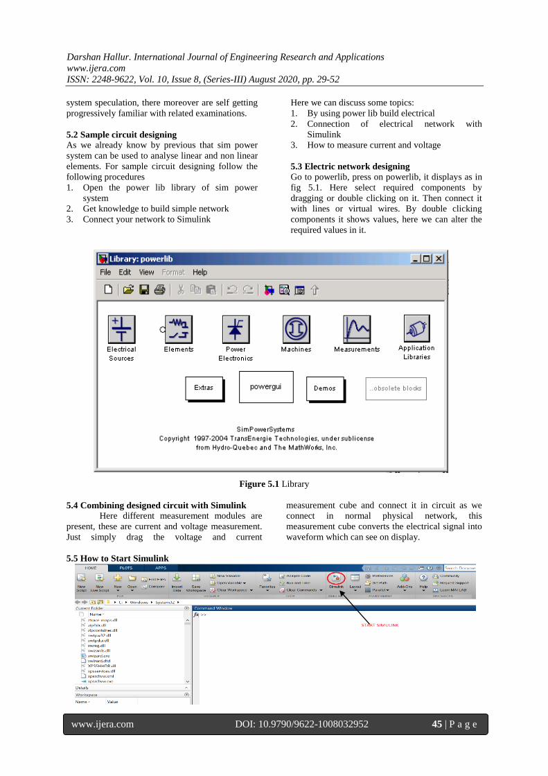
Go to powerlib, press on powerlib, it displays as in
fig 5.1. Here select required components by
dragging or double clicking on it. Then connect it
with lines or virtual wires. By double clicking
components it shows values, here we can alter the
required values in it.
Figure 5.1 Library
5.4 Combining designed circuit with Simulink
Here different measurement modules are
present, these are current and voltage measurement.
Just simply drag the voltage and current
measurement cube and connect it in circuit as we
connect in normal physical network, this
measurement cube converts the electrical signal into
waveform which can see on display.
5.5 How to Start Simulink
Darshan Hallur. International Journal of Engineering Research and Applications
www.ijera.com
ISSN: 2248-9622, Vol. 10, Issue 8, (Series-III) August 2020, pp. 29-52
www.ijera.com DOI: 10.9790/9622-1008032952 46 | P a g e
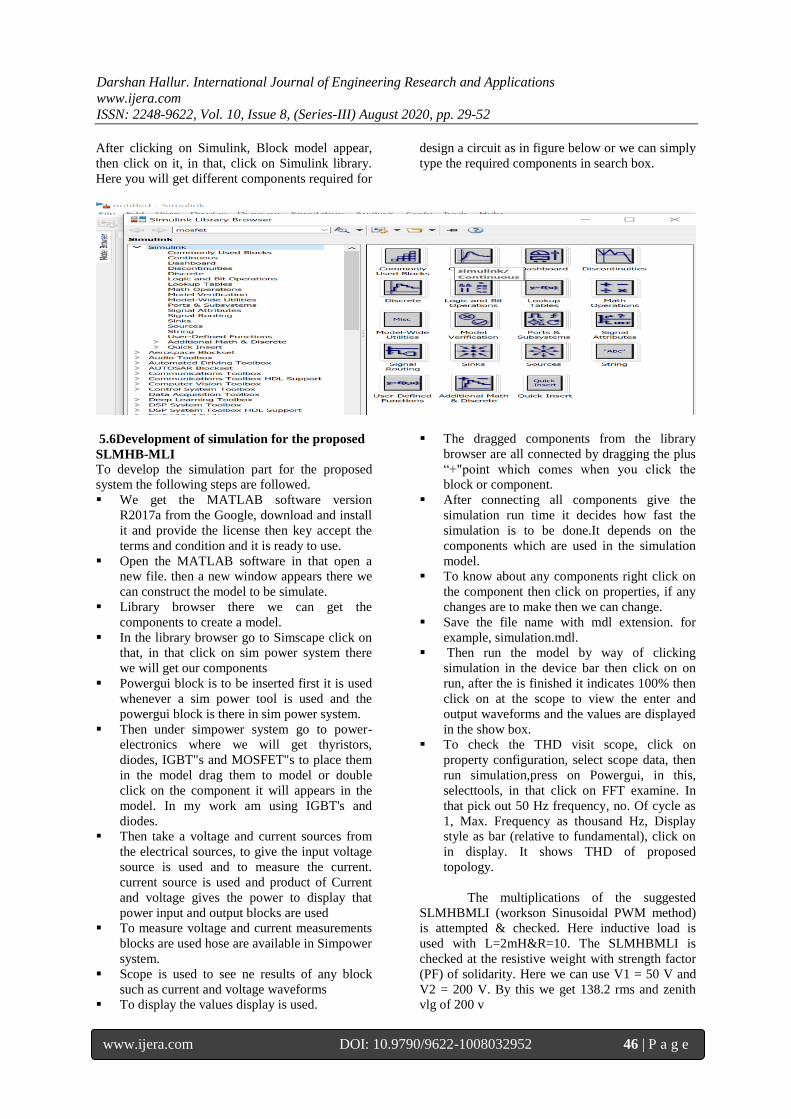
After clicking on Simulink, Block model appear,
then click on it, in that, click on Simulink library.
Here you will get different components required for
design a circuit as in figure below or we can simply
type the required components in search box.
5.6Development of simulation for the proposed
SLMHB-MLI
To develop the simulation part for the proposed
system the following steps are followed.
We get the MATLAB software version
R2017a from the Google, download and install
it and provide the license then key accept the
terms and condition and it is ready to use.
Open the MATLAB software in that open a
new file. then a new window appears there we
can construct the model to be simulate.
Library browser there we can get the
components to create a model.
In the library browser go to Simscape click on
that, in that click on sim power system there
we will get our components
Powergui block is to be inserted first it is used
whenever a sim power tool is used and the
powergui block is there in sim power system.
Then under simpower system go to power-
electronics where we will get thyristors,
diodes, IGBT"s and MOSFET"s to place them
in the model drag them to model or double
click on the component it will appears in the
model. In my work am using IGBT's and
diodes.
Then take a voltage and current sources from
the electrical sources, to give the input voltage
source is used and to measure the current.
current source is used and product of Current
and voltage gives the power to display that
power input and output blocks are used
To measure voltage and current measurements
blocks are used hose are available in Simpower
system.
Scope is used to see ne results of any block
such as current and voltage waveforms
To display the values display is used.
The dragged components from the library
browser are all connected by dragging the plus
―+"point which comes when you click the
block or component.
After connecting all components give the
simulation run time it decides how fast the
simulation is to be done.It depends on the
components which are used in the simulation
model.
To know about any components right click on
the component then click on properties, if any
changes are to make then we can change.
Save the file name with mdl extension. for
example, simulation.mdl.
Then run the model by way of clicking
simulation in the device bar then click on on
run, after the is finished it indicates 100% then
click on at the scope to view the enter and
output waveforms and the values are displayed
in the show box.
To check the THD visit scope, click on
property configuration, select scope data, then
run simulation,press on Powergui, in this,
selecttools, in that click on FFT examine. In
that pick out 50 Hz frequency, no. Of cycle as
1, Max. Frequency as thousand Hz, Display
style as bar (relative to fundamental), click on
in display. It shows THD of proposed
topology.
The multiplications of the suggested
SLMHBMLI (workson Sinusoidal PWM method)
is attempted & checked. Here inductive load is
used with L=2mH&R=10. The SLMHBMLI is
checked at the resistive weight with strength factor
(PF) of solidarity. Here we can use V1 = 50 V and
V2 = 200 V. By this we get 138.2 rms and zenith
vlg of 200 v
Darshan Hallur. International Journal of Engineering Research and Applications
www.ijera.com
ISSN: 2248-9622, Vol. 10, Issue 8, (Series-III) August 2020, pp. 29-52
www.ijera.com DOI: 10.9790/9622-1008032952 47 | P a g e
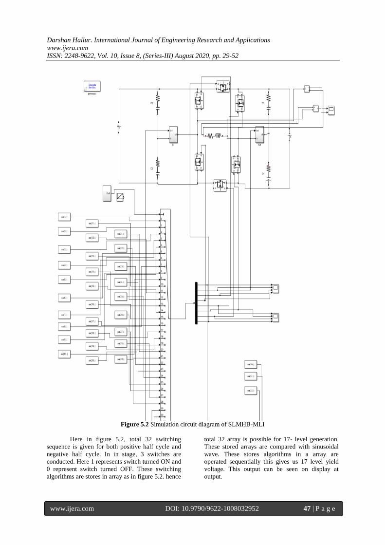
Figure 5.2 Simulation circuit diagram of SLMHB-MLI
Here in figure 5.2, total 32 switching
sequence is given for both positive half cycle and
negative half cycle. In in stage, 3 switches are
conducted. Here 1 represents switch turned ON and
0 represent switch turned OFF. These switching
algorithms are stores in array as in figure 5.2. hence
total 32 array is possible for 17- level generation.
These stored arrays are compared with sinusoidal
wave. These stores algorithms in a array are
operated sequentially this gives us 17 level yield
voltage. This output can be seen on display at
output.
Darshan Hallur. International Journal of Engineering Research and Applications
www.ijera.com
ISSN: 2248-9622, Vol. 10, Issue 8, (Series-III) August 2020, pp. 29-52
www.ijera.com DOI: 10.9790/9622-1008032952 48 | P a g e
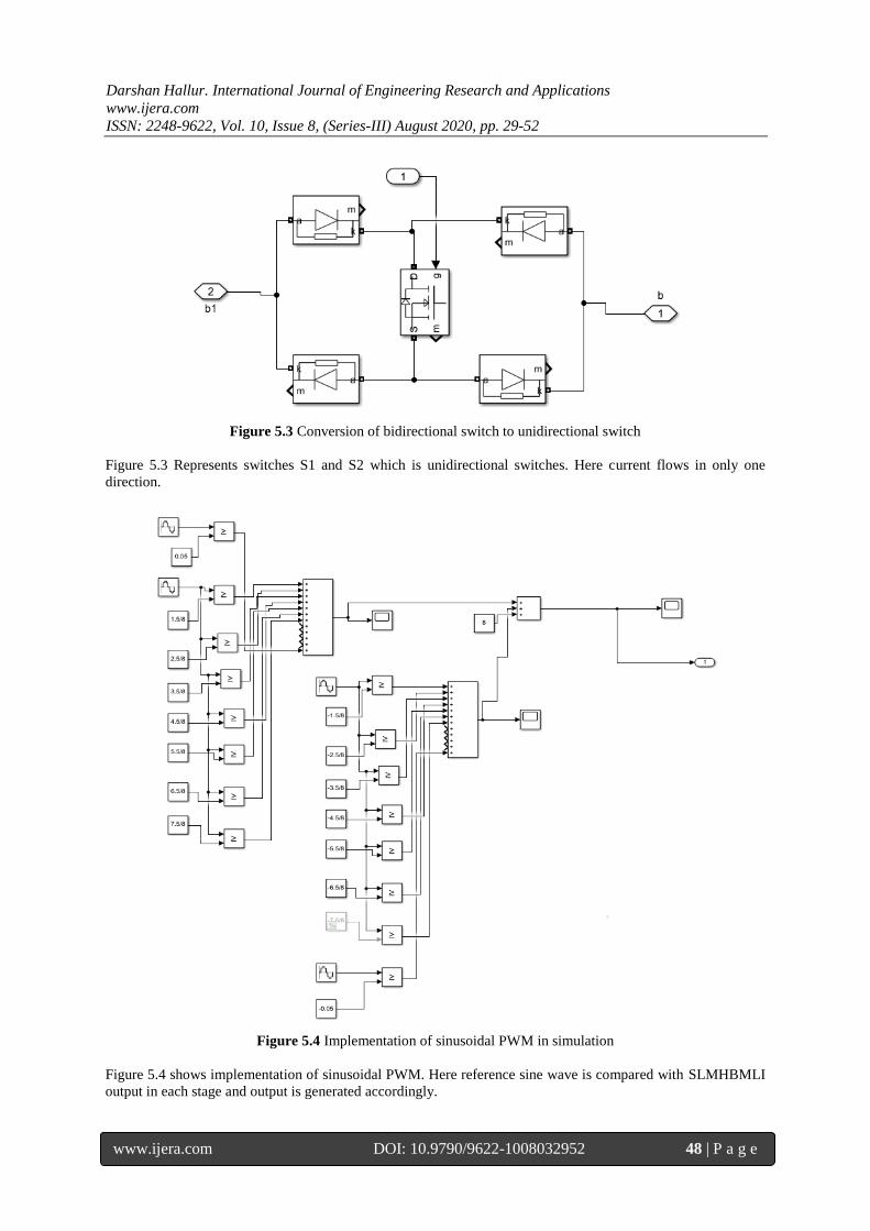
Figure 5.3 Conversion of bidirectional switch to unidirectional switch
Figure 5.3 Represents switches S1 and S2 which is unidirectional switches. Here current flows in only one
direction.
Figure 5.4 Implementation of sinusoidal PWM in simulation
Figure 5.4 shows implementation of sinusoidal PWM. Here reference sine wave is compared with SLMHBMLI
output in each stage and output is generated accordingly.
Darshan Hallur. International Journal of Engineering Research and Applications
www.ijera.com
ISSN: 2248-9622, Vol. 10, Issue 8, (Series-III) August 2020, pp. 29-52
www.ijera.com DOI: 10.9790/9622-1008032952 49 | P a g e
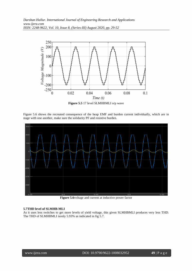
Figure 5.5 17 level SLMHBMLI o/p wave
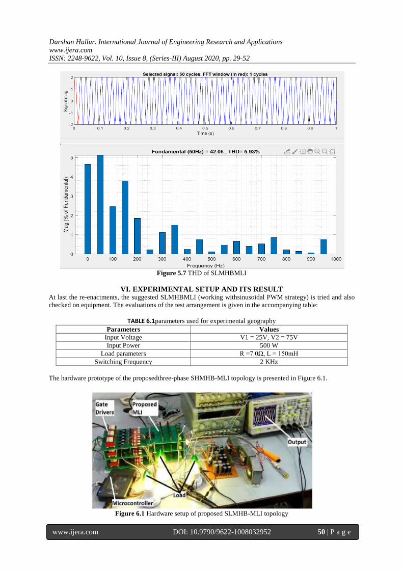
Figure 5.6 shows the recreated consequence of the heap EMF and burden current individually, which are in
stage with one another, make sure the solidarity PF and resistive burden.
Figure 5.6voltage and current at inductive power factor
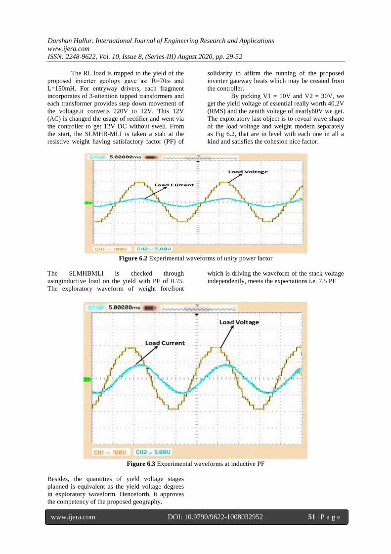
5.7THD level of SLMHB-MLI
As it uses less switches to get more levels of yield voltage, this given SLMHBMLI produces very less THD.
The THD of SLMHBMLI isonly 5.93% as indicated in fig 5.7.
Darshan Hallur. International Journal of Engineering Research and Applications
www.ijera.com
ISSN: 2248-9622, Vol. 10, Issue 8, (Series-III) August 2020, pp. 29-52
www.ijera.com DOI: 10.9790/9622-1008032952 50 | P a g e
Figure 5.7 THD of SLMHBMLI
VI. EXPERIMENTAL SETUP AND ITS RESULT At last the re-enactments, the suggested SLMHBMLI (working withsinusoidal PWM strategy) is tried and also
checked on equipment. The evaluations of the test arrangement is given in the accompanying table:
TABLE 6.1parameters used for experimental geography
Parameters Values
Input Voltage V1 = 25V, V2 = 75V
Input Power 500 W
Load parameters R =7 0Ω, L = 150mH
Switching Frequency 2 KHz
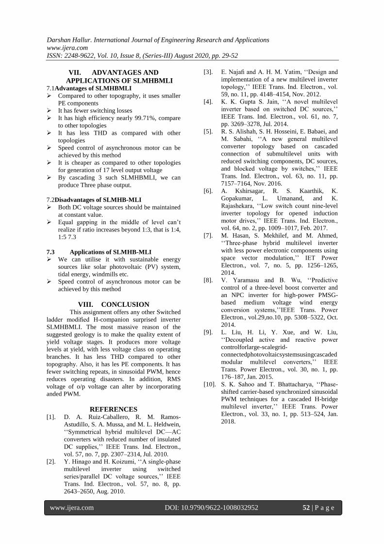
The hardware prototype of the proposedthree-phase SHMHB-MLI topology is presented in Figure 6.1.
Figure 6.1 Hardware setup of proposed SLMHB-MLI topology
Darshan Hallur. International Journal of Engineering Research and Applications
www.ijera.com
ISSN: 2248-9622, Vol. 10, Issue 8, (Series-III) August 2020, pp. 29-52
www.ijera.com DOI: 10.9790/9622-1008032952 51 | P a g e
The RL load is trapped to the yield of the
proposed inverter geology gave as: R=70ω and
L=150mH. For entryway drivers, each fragment
incorporates of 3-attention tapped transformers and
each transformer provides step down movement of
the voltage.it converts 220V to 12V. This 12V
(AC) is changed the usage of rectifier and went via
the controller to get 12V DC without swell. From
the start, the SLMHB-MLI is taken a stab at the
resistive weight having satisfactory factor (PF) of
solidarity to affirm the running of the proposed
inverter gateway beats which may be created from
the controller.
By picking V1 = 10V and V2 = 30V, we
get the yield voltage of essential really worth 40.2V
(RMS) and the zenith voltage of nearly60V we get.
The exploratory last object is to reveal wave shape
of the load voltage and weight modern separately
as Fig 6.2, that are in level with each one in all a
kind and satisfies the cohesion nice factor.
Figure 6.2 Experimental waveforms of unity power factor
The SLMHBMLI is checked through
usinginductive load on the yield with PF of 0.75.
The exploratory waveform of weight forefront
which is driving the waveform of the stack voltage
independently, meets the expectations i.e. 7.5 PF
Figure 6.3 Experimental waveforms at inductive PF
Besides, the quantities of yield voltage stages
planned is equivalent as the yield voltage degrees
in exploratory waveform. Henceforth, it approves
the competency of the proposed geography.
Darshan Hallur. International Journal of Engineering Research and Applications
www.ijera.com
ISSN: 2248-9622, Vol. 10, Issue 8, (Series-III) August 2020, pp. 29-52
www.ijera.com DOI: 10.9790/9622-1008032952 52 | P a g e
VII. ADVANTAGES AND
APPLICATIONS OF SLMHBMLI 7.1Advantages of SLMHBMLI
Compared to other topography, it uses smaller
PE components
It has fewer switching losses
It has high efficiency nearly 99.71%, compare
to other topologies
It has less THD as compared with other
topologies
Speed control of asynchronous motor can be
achieved by this method
It is cheaper as compared to other topologies
for generation of 17 level output voltage
By cascading 3 such SLMHBMLI, we can
produce Three phase output.
7.2Disadvantages of SLMHB-MLI
Both DC voltage sources should be maintained
at constant value.
Equal gapping in the middle of level can’t
realize if ratio increases beyond 1:3, that is 1:4,
1:5 7.3
7.3 Applications of SLMHB-MLI We can utilise it with sustainable energy
sources like solar photovoltaic (PV) system,
tidal energy, windmills etc.
Speed control of asynchronous motor can be
achieved by this method
VIII. CONCLUSION This assignment offers any other Switched
ladder modified H-companion surprised inverter
SLMHBMLI. The most massive reason of the
suggested geology is to make the quality extent of
yield voltage stages. It produces more voltage
levels at yield, with less voltage class on operating
branches. It has less THD compared to other
topography. Also, it has les PE components. It has
fewer switching repeats, in sinusoidal PWM, hence
reduces operating disasters. In addition, RMS
voltage of o/p voltage can alter by incorporating
anded PWM.
REFERENCES [1]. D. A. Ruiz-Caballero, R. M. Ramos-
Astudillo, S. A. Mussa, and M. L. Heldwein,
‘‘Symmetrical hybrid multilevel DC—AC
converters with reduced number of insulated
DC supplies,’’ IEEE Trans. Ind. Electron.,
vol. 57, no. 7, pp. 2307–2314, Jul. 2010.
[2]. Y. Hinago and H. Koizumi, ‘‘A single-phase
multilevel inverter using switched
series/parallel DC voltage sources,’’ IEEE
Trans. Ind. Electron., vol. 57, no. 8, pp.
2643–2650, Aug. 2010.
[3]. E. Najafi and A. H. M. Yatim, ‘‘Design and
implementation of a new multilevel inverter
topology,’’ IEEE Trans. Ind. Electron., vol.
59, no. 11, pp. 4148–4154, Nov. 2012.
[4]. K. K. Gupta S. Jain, ‘‘A novel multilevel
inverter based on switched DC sources,’’
IEEE Trans. Ind. Electron., vol. 61, no. 7,
pp. 3269–3278, Jul. 2014.
[5]. R. S. Alishah, S. H. Hosseini, E. Babaei, and
M. Sabahi, ‘‘A new general multilevel
converter topology based on cascaded
connection of submultilevel units with
reduced switching components, DC sources,
and blocked voltage by switches,’’ IEEE
Trans. Ind. Electron., vol. 63, no. 11, pp.
7157–7164, Nov. 2016.
[6]. A. Kshirsagar, R. S. Kaarthik, K.
Gopakumar, L. Umanand, and K.
Rajashekara, ‘‘Low switch count nine-level
inverter topology for opened induction
motor drives,’’ IEEE Trans. Ind. Electron.,
vol. 64, no. 2, pp. 1009–1017, Feb. 2017.
[7]. M. Hasan, S. Mekhilef, and M. Ahmed,
‘‘Three-phase hybrid multilevel inverter
with less power electronic components using
space vector modulation,’’ IET Power
Electron., vol. 7, no. 5, pp. 1256–1265,
2014.
[8]. V. Yaramasu and B. Wu, ‘‘Predictive
control of a three-level boost converter and
an NPC inverter for high-power PMSG-
based medium voltage wind energy
conversion systems,’’IEEE Trans. Power
Electron., vol.29,no.10, pp. 5308–5322, Oct.
2014.
[9]. L. Liu, H. Li, Y. Xue, and W. Liu,
‘‘Decoupled active and reactive power
controlforlarge-scalegrid-
connectedphotovoltaicsystemsusingcascaded
modular multilevel converters,’’ IEEE
Trans. Power Electron., vol. 30, no. 1, pp.
176–187, Jan. 2015.
[10]. S. K. Sahoo and T. Bhattacharya, ‘‘Phase-
shifted carrier-based synchronized sinusoidal
PWM techniques for a cascaded H-bridge
multilevel inverter,’’ IEEE Trans. Power
Electron., vol. 33, no. 1, pp. 513–524, Jan.
2018.
Related Documents


