GaN for Green Future CONFIDENTIAL 1 New GaN Platform enabling High-efficiency and Small-size High-power Electronic Systems Yuanshan Advanced Material Technologies Inc.

Welcome message from author
This document is posted to help you gain knowledge. Please leave a comment to let me know what you think about it! Share it to your friends and learn new things together.
Transcript
GaN for Green Future
CONFIDENTIAL 1
New GaN Platform
enabling
High-efficiency and Small-size
High-power Electronic Systems
Yuanshan Advanced Material Technologies Inc.
GaN for Green Future
CONFIDENTIAL 2
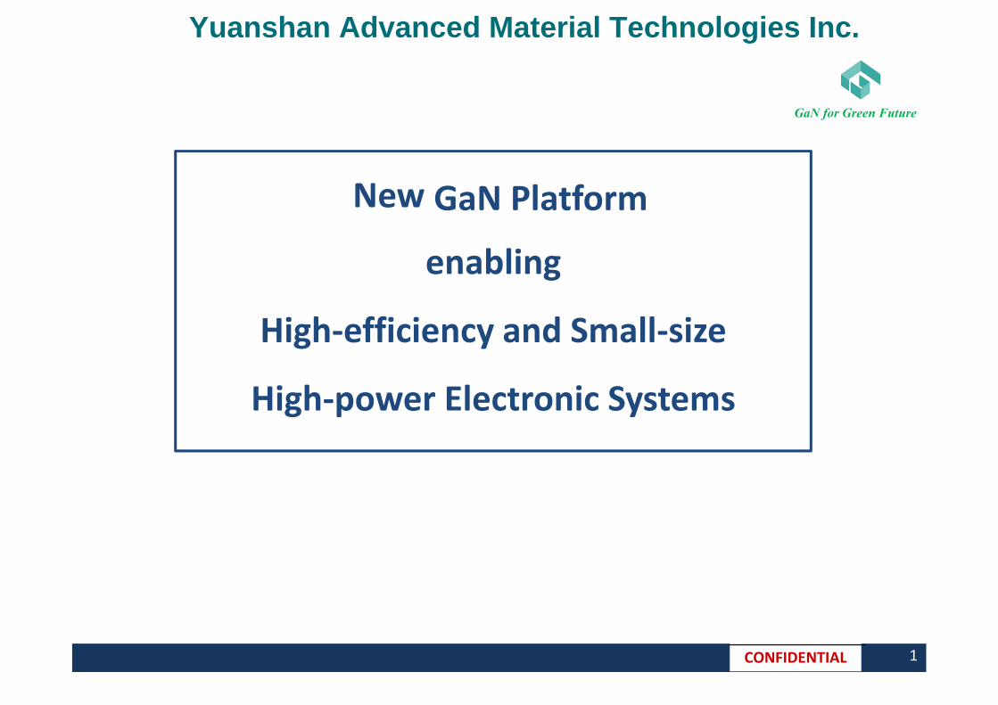
Established:Location:Capital: ¥200MEmployee :
Business: GaN epitaxial wafers, Developing GaN electronic devices
上海
October 2017Jining City, 272000 Shandong, China
50
Yuanshan Advanced Material Technologies Inc.
GaN for Green Future
CONFIDENTIAL 3
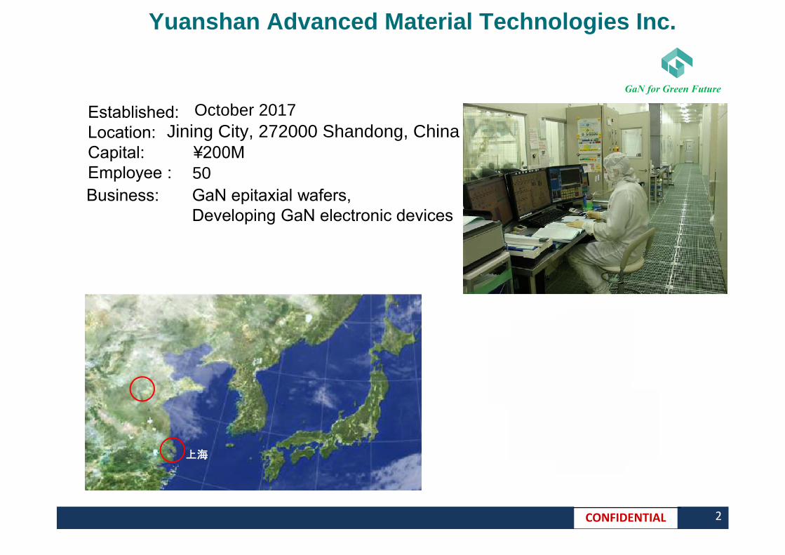
World first F100 mm GaN HEMT wafer
World first 600 [V] vertical GaN Shottky diode
Invention of Polarization Super-junction Transistor
World first 1,000 [V] switching
New vertical 8-inch multi-wafer MOCVD reactor
3,300 [V] GaN PSJ power transistor
10,000 [V] power transistor and 8,000 [V] Schottky diode
Developing GaN power modlues
Wind-turbine
Achievement
GaN MOCVD Reactor
52 mm
32 mm
HV LVOUT
1,650 V
GaN chip
Yuanshan Advanced Material Technologies Inc.
GaN for Green Future
CONFIDENTIAL 4
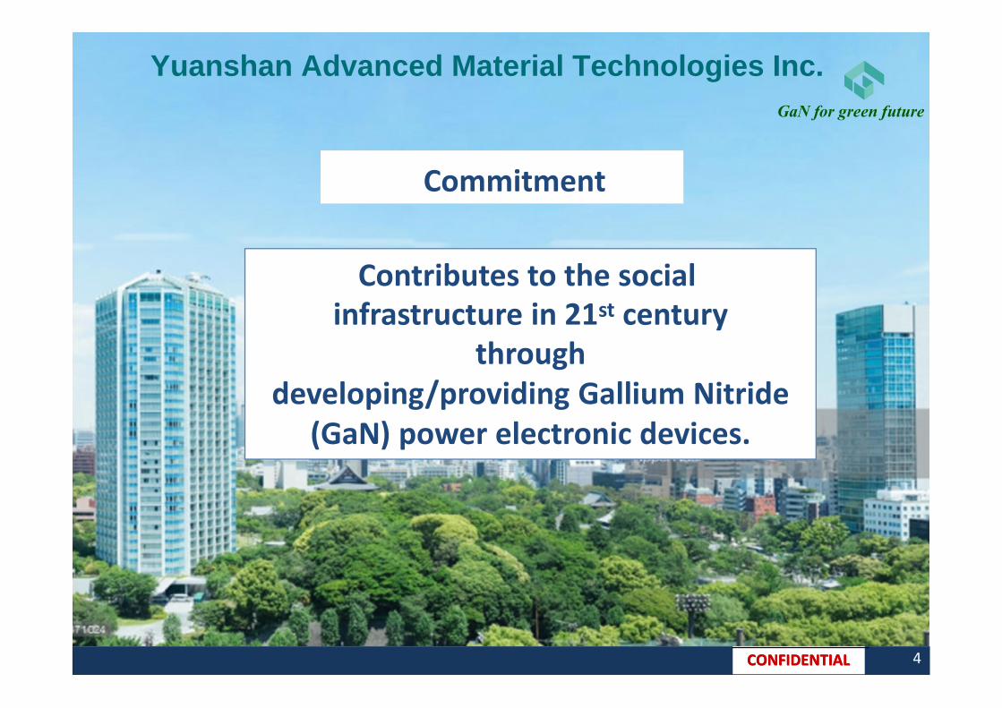
Contributes to the social infrastructure in 21st century
through developing/providing Gallium Nitride
(GaN) power electronic devices.
Commitment
GaN for green future
CONFIDENTIAL
Yuanshan Advanced Material Technologies Inc.
GaN for Green Future
CONFIDENTIAL 5
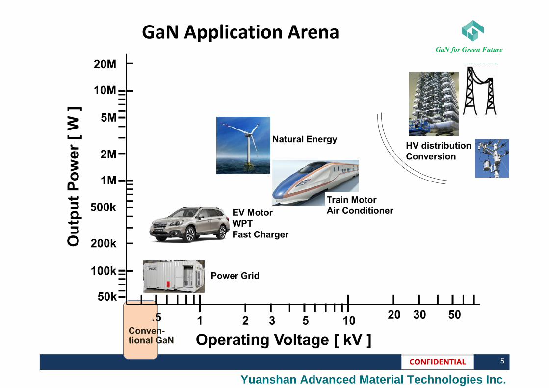
.5 1 2 3 105 20 30 50
Operating Voltage [ kV ]
50k
500k
200k
100k
1M
2M
5M
10M
20MO
utp
ut
Po
wer
[ W
]
GaN Application Arena
Power Grid
EV MotorWPTFast Charger
Natural Energy
Train MotorAir Conditioner
HV distributionConversion
Conven-tional GaN
Yuanshan Advanced Material Technologies Inc.
GaN for Green Future
CONFIDENTIAL 6
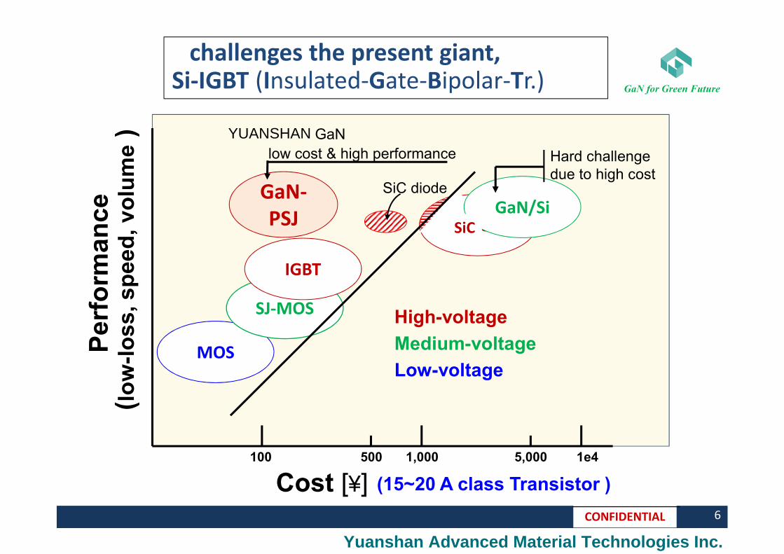
challenges the present giant, Si-IGBT (Insulated-Gate-Bipolar-Tr.)
Perf
orm
an
ce
( lo
w-l
oss, sp
eed
, vo
lum
e)
Cost [¥]
GaN-PSJ
MOS
SJ-MOS
SiC
Low-voltage
High-voltage
Hard challenge due to high cost
GaN
low cost & high performance
Medium-voltage
SiC diode
1,000 5,000500100 1e4
(15~20 A class Transistor )
IGBT
GaN/SiSiC
Yuanshan Advanced Material Technologies Inc.
YUANSHAN
GaN for Green Future
CONFIDENTIAL 7
10-9
10-8
10-7
10-6
10-5
10-4
0 2 4 6 8 10
off state
Dra
in C
urr
en
t [A
]
Drain Voltage [kV]
Vg : -10 V
Lpsj : 100 mmWg : 100 mm
today’s Achievement
D(排出)S(源)
G(扉)
VGS(扉電圧)
0
1
2
3
4
5
6
7
0 2 4 6 8 10
IdVd
Dra
in C
urr
en
t [A
]
Drain Voltage [V]
Vg : +2 V
0 V
-2 V
-4, -6 V
Lpsj : 100 mmWg : 100 mm
Ron :
805 m
D(排出)S(源)
G(扉)
VDS = 印加電圧
(I) GaN Transistor : Breakdown voltage > 10 kV
Yuanshan Advanced Material Technologies Inc.
GaN for Green Future
CONFIDENTIAL 8
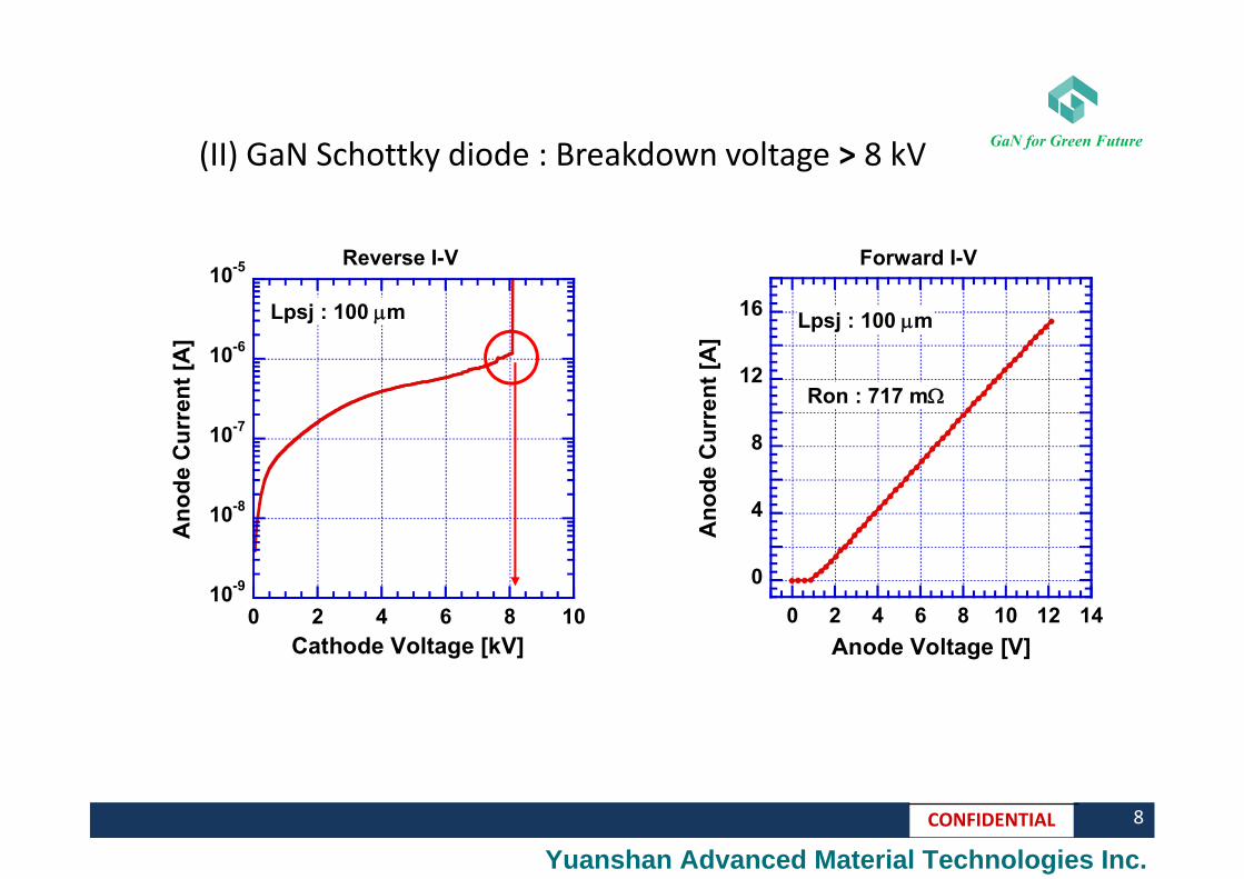
(II) GaN Schottky diode : Breakdown voltage > 8 kV
10-9
10-8
10-7
10-6
10-5
0 2 4 6 8 10
Reverse I-V
An
od
e C
urr
en
t [A
]
Cathode Voltage [kV]
Lpsj : 100 mm
0
4
8
12
16
0 2 4 6 8 10 12 14
Forward I-V
An
od
e C
urr
en
t [A
]
Anode Voltage [V]
Ron : 717 m
Lpsj : 100 mm
Yuanshan Advanced Material Technologies Inc.
GaN for Green Future
CONFIDENTIAL 10
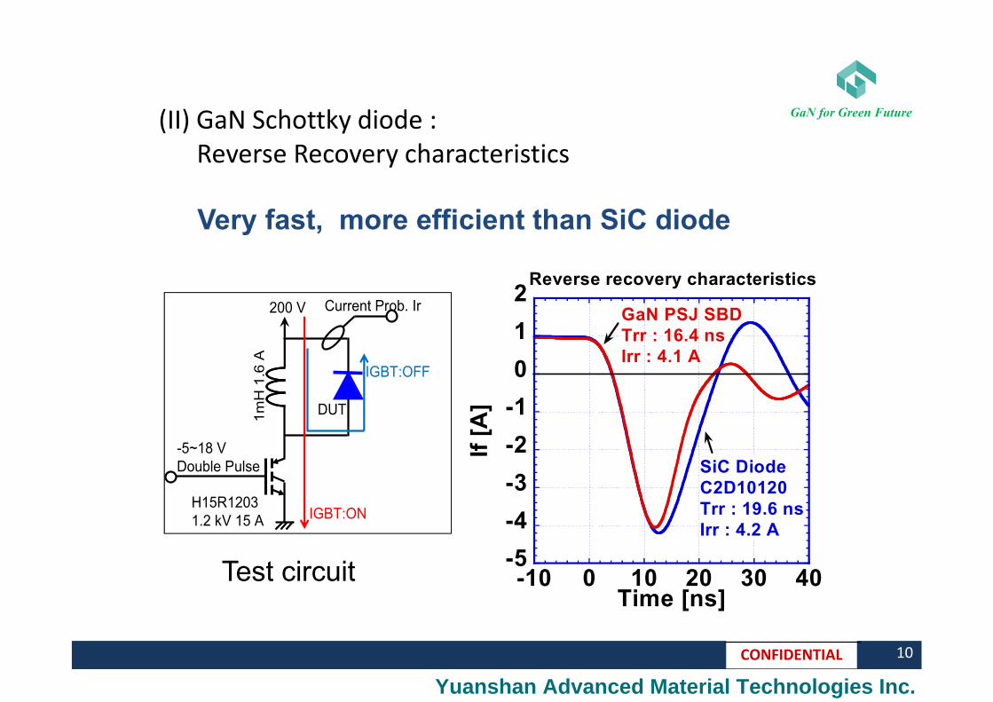
(II) GaN Schottky diode : Reverse Recovery characteristics
-5~18 VDouble Pulse
DUT
1m
H 1
.6 A
200 V
IGBT:ON
IGBT:OFF
Current Prob. Ir
H15R12031.2 kV 15 A
-5
-4
-3
-2
-1
0
1
2
-10 0 10 20 30 40
Reverse recovery characteristics
If [
A]
Time [ns]
GaN PSJ SBDTrr : 16.4 nsIrr : 4.1 A
SiC DiodeC2D10120Trr : 19.6 nsIrr : 4.2 A
Very fast, more efficient than SiC diode
Test circuit
Yuanshan Advanced Material Technologies Inc.
GaN for Green Future
CONFIDENTIAL
IGBT
GaN-FET
GaN FET : 1650 V / 5 A
(III) GaN FET : Comparison of switching-loss with IGBT
1,650 V
Double-pulse method
16501200900600
Input voltage [V]S
wit
ch
ing
lo
ss [m
J]
Yuanshan Advanced Material Technologies Inc.
GaN for Green Future
CONFIDENTIAL 12
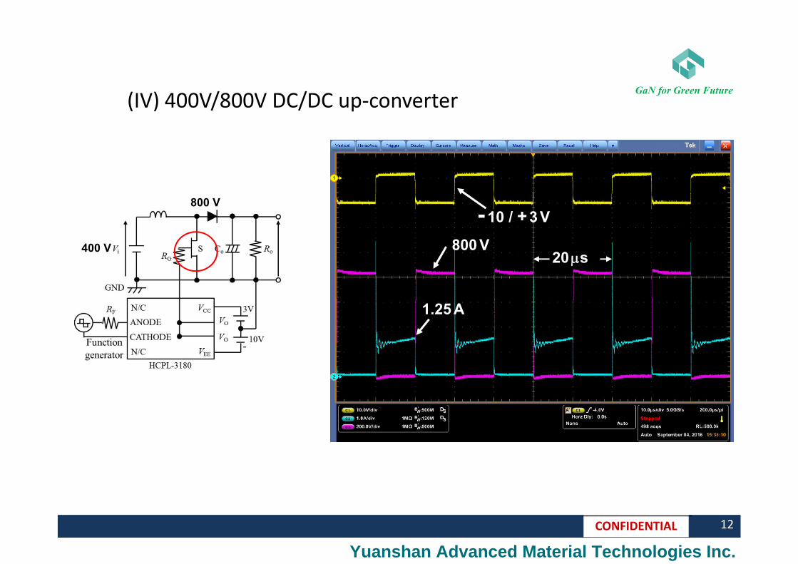
(IV) 400V/800V DC/DC up-converter
400 V
800 V
1.25 A
800 V
-10 / +3 V
20ms
Yuanshan Advanced Material Technologies Inc.
GaN for Green Future
CONFIDENTIAL
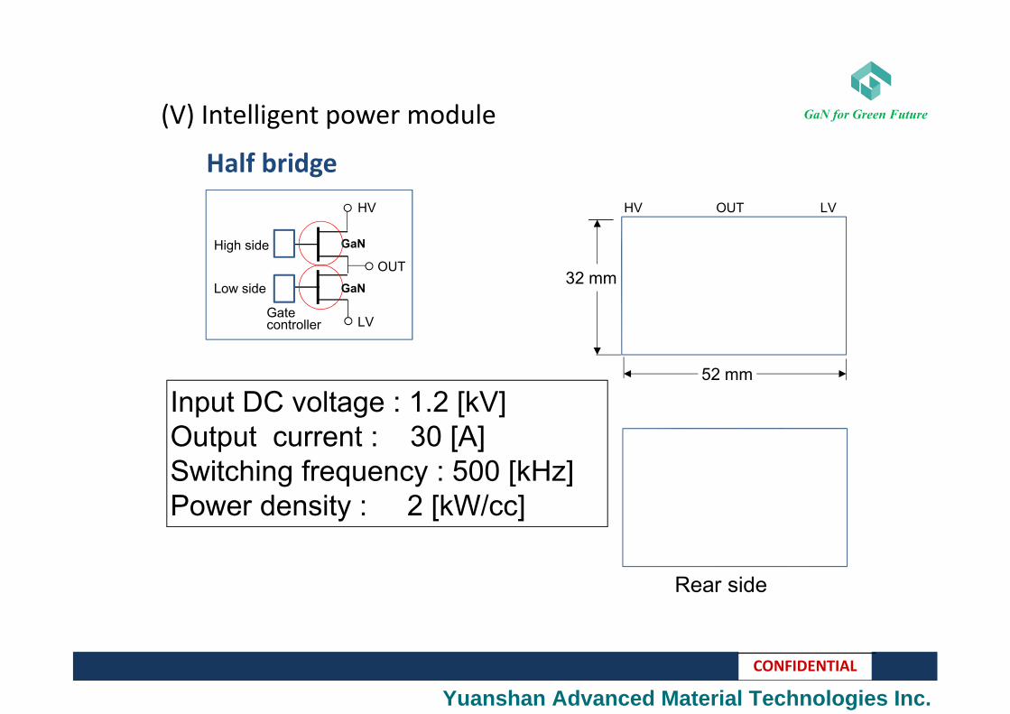
(V) Intelligent power module
Half bridge
Input DC voltage : 1.2 [kV]Output current : 30 [A]Switching frequency : 500 [kHz]Power density : 2 [kW/cc]
Rear side
High side
Low side
HV
LV
OUT
Gate controller
GaN
GaN
52 mm
32 mm
HV LVOUT
Yuanshan Advanced Material Technologies Inc.
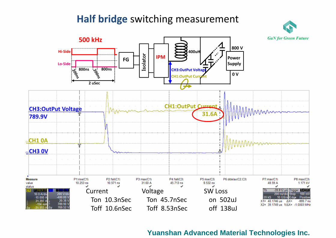
Half bridge switching measurement
CurrentTon 10.3nSecToff 10.6nSec
VoltageTon 45.7nSecToff 8.53nSec
CH1:OutPut Current31.6A
CH3:OutPut Voltage789.9V
SW Losson 502uJoff 138uJ
500 kHz
Hi-Side
Lo-Side
800ns 800ns
2 uSec
CH3 0V
CH1 0AIsolator
FG
400uH
CH3:OutPut Voltage
CH1:OutPut Current
800 V
0 V
Power Supply
IPM
GaN for Green Future
Yuanshan Advanced Material Technologies Inc.
GaN for Green Future
CONFIDENTIAL 15
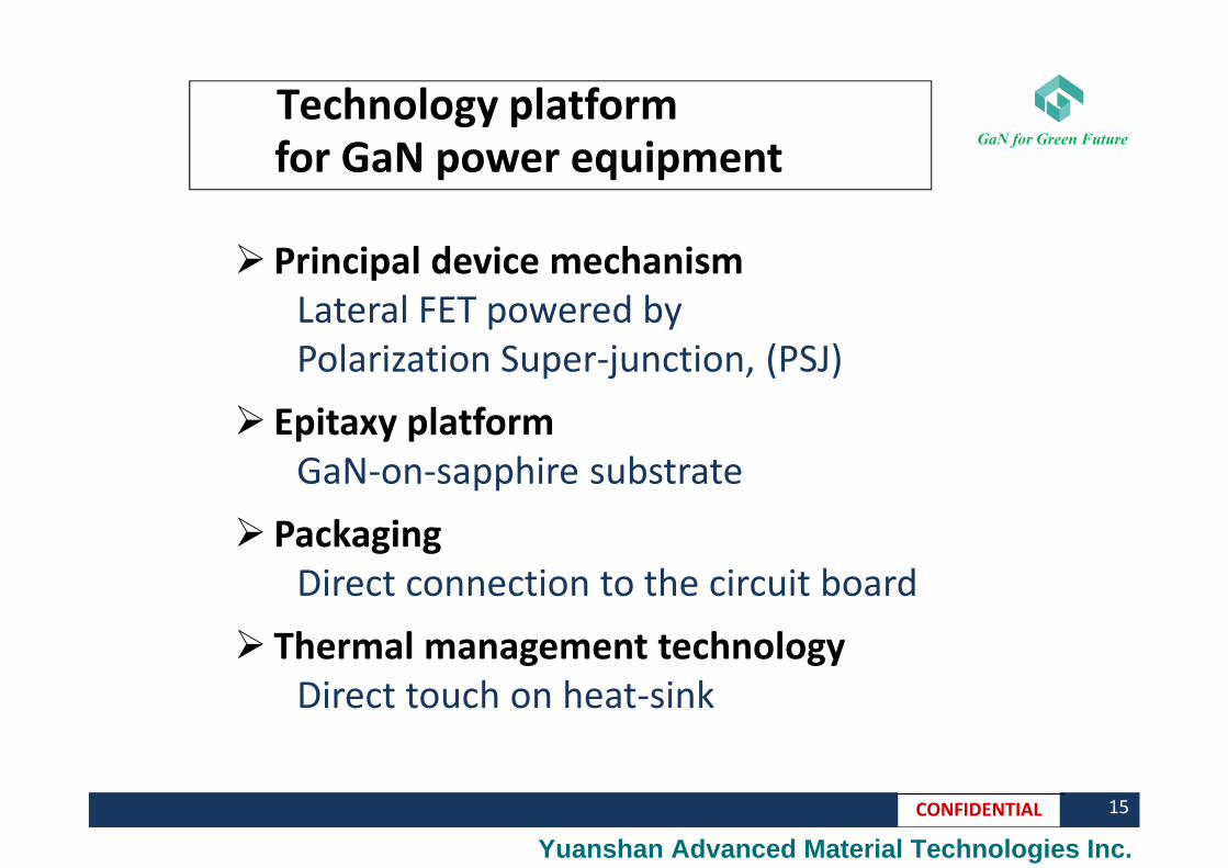
Technology platform for GaN power equipment
Principal device mechanismLateral FET powered by Polarization Super-junction, (PSJ)
Epitaxy platformGaN-on-sapphire substrate
PackagingDirect connection to the circuit board
Thermal management technologyDirect touch on heat-sink
Yuanshan Advanced Material Technologies Inc.
GaN for Green Future
CONFIDENTIAL 16
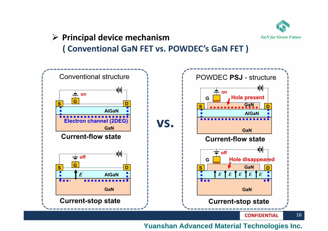
Principal device mechanism( Conventional GaN FET vs. POWDEC’s GaN FET )
S D
AlGaN
GaN
G
Conventional structure POWDEC PSJ - structure
vs.Electron channel (2DEG)
on
Current-flow state
S D
AlGaN
GaN
G
off
E
Current-stop state
S
GaN
G
D
AlGaN
GaN
Hole presenton
S
GaN
G
DGaN
Hole disappeared
off
E E E E E
Current-flow state
Current-stop state
Yuanshan Advanced Material Technologies Inc.
GaN for Green Future
CONFIDENTIAL 17
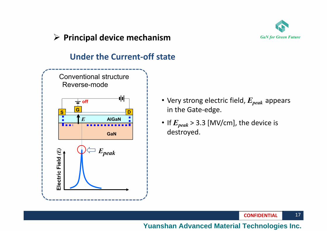
Principal device mechanism
Ele
ctr
ic F
ield
(E
)
Conventional structure
S D
AlGaN
GaN
G
off
E
Reverse-mode
Epeak
Under the Current-off state
• Very strong electric field, Epeak appears in the Gate-edge.
• If Epeak > 3.3 [MV/cm], the device is destroyed.
Yuanshan Advanced Material Technologies Inc.
GaN for Green Future
CONFIDENTIAL 18
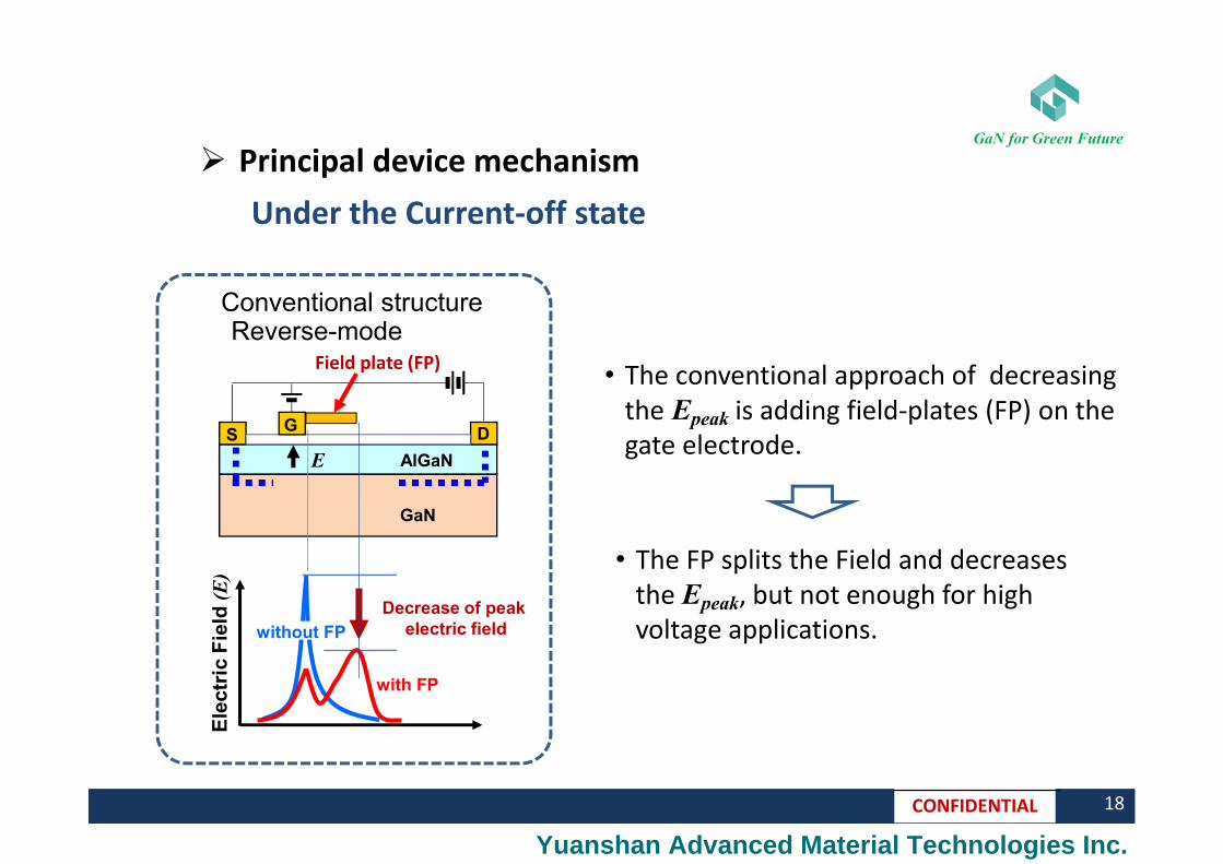
Principal device mechanism
Field plate (FP)
Ele
ctr
ic F
ield
(E
)
without FP
with FP
Decrease of peak electric field
Conventional structureReverse-mode
S D
AlGaN
GaN
G
E
Under the Current-off state
• The conventional approach of decreasing the Epeak is adding field-plates (FP) on the gate electrode.
• The FP splits the Field and decreases the Epeak, but not enough for high voltage applications.
Yuanshan Advanced Material Technologies Inc.
GaN for Green Future
CONFIDENTIAL 19
Field plate (FP)
Ele
ctr
ic F
ield
(E
)
without FP
with FP
Decrease of peak electric field
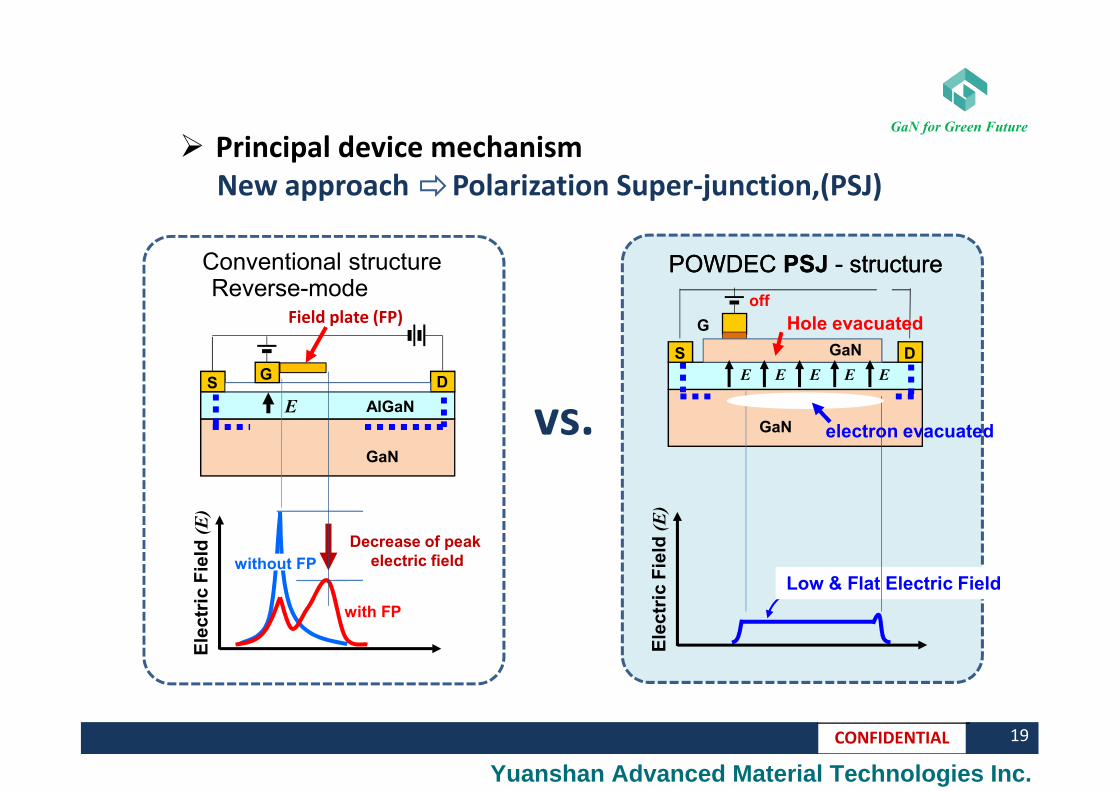
Conventional structure
vs.
Reverse-mode
S D
AlGaN
GaN
G
E
Principal device mechanismNew approach Polarization Super-junction,(PSJ)
POWDEC PSJ - structure
Ele
ctr
ic F
ield
(E
)
POWDEC PSJ - structure
Low & Flat Electric Field
S
GaN
G
DGaN
Hole evacuated
off
E E E E E
electron evacuated
Yuanshan Advanced Material Technologies Inc.
GaN for Green Future
CONFIDENTIAL 20
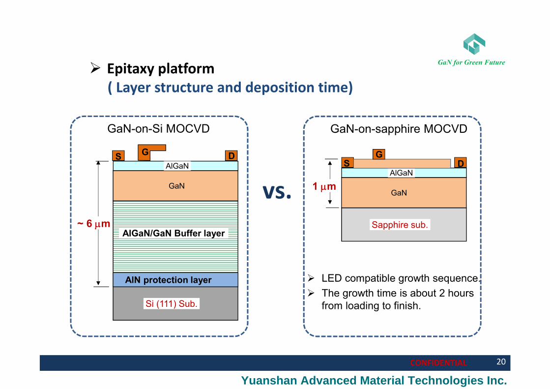
Epitaxy platform( Layer structure and deposition time)
~ 6 mm
GaN
AlGaN/GaN Buffer layer
Si (111) Sub.
AlN protection layer
AlGaNS DG
Sapphire sub.
GaN
AlGaNS D
G
1 mm
GaN-on-Si MOCVD GaN-on-sapphire MOCVD
LED compatible growth sequence.
The growth time is about 2 hours from loading to finish.
vs.
Yuanshan Advanced Material Technologies Inc.
GaN for Green Future
CONFIDENTIAL 21
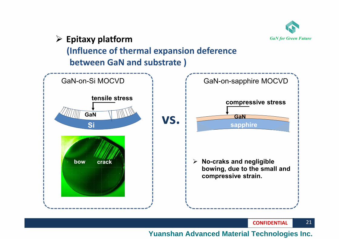
Epitaxy platform(Influence of thermal expansion deference between GaN and substrate )
Si
GaN vs.
crackbow
GaN-on-Si MOCVD GaN-on-sapphire MOCVD
GaN
sapphire
tensile stresscompressive stress
No-craks and negligible bowing, due to the small and compressive strain.
Yuanshan Advanced Material Technologies Inc.
GaN for Green Future
CONFIDENTIAL
repeat
22
Epitaxy platform(MOCVD deposition sequence)
Si wafer setting GaN deposition
Cleaning
(Out-situ)
Baking
(In-situ)
GaN depo-ed
Carrier ‘ finished’
wafers
repeat +
GaN-on-Si
Sapphire wafer setting GaN deposition
+
GaN depo-ed
Carrier
‘ finished’wafers
GaN-on-Sapphire
vs.
The growth can run consecutively many times without interruption.
Yuanshan Advanced Material Technologies Inc.
GaN for Green Future
CONFIDENTIAL 23
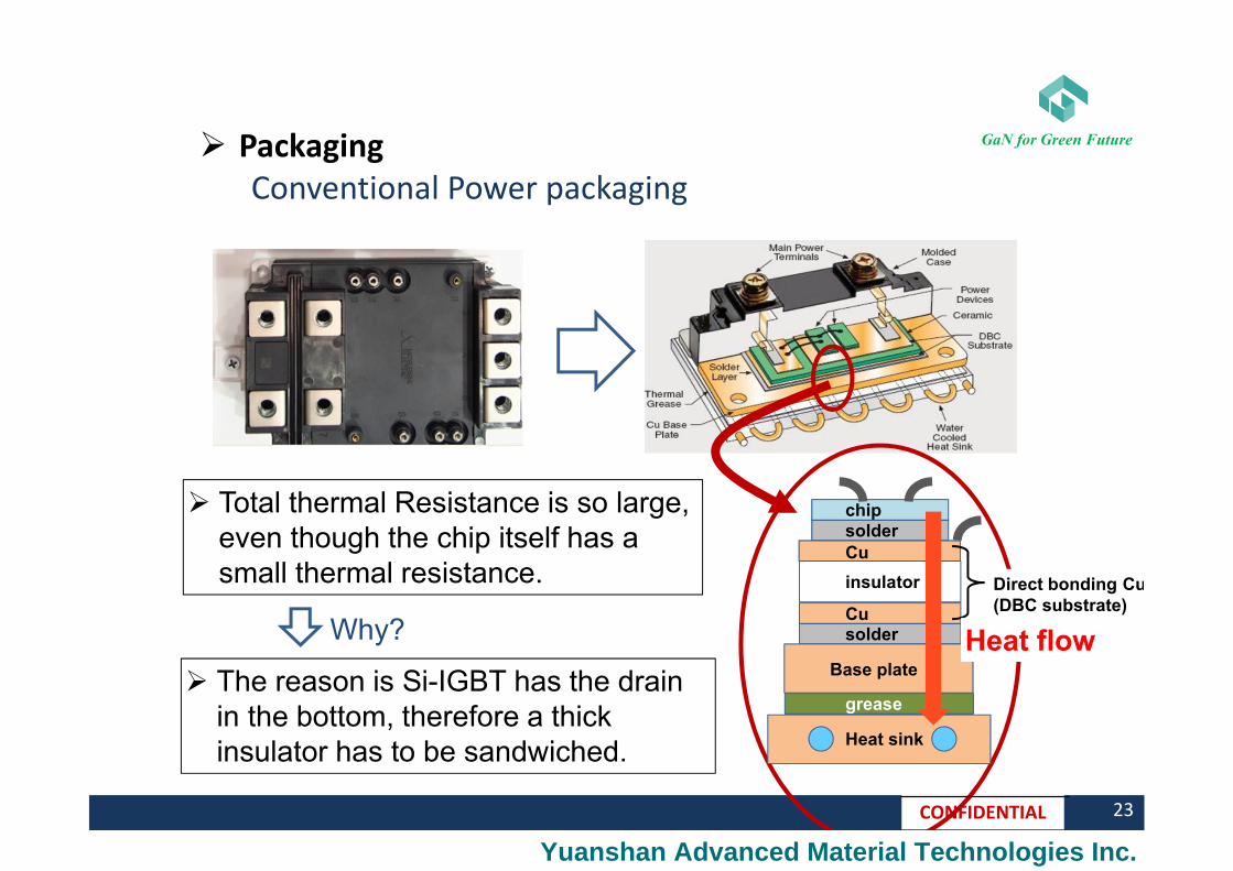
PackagingConventional Power packaging
Total thermal Resistance is so large, even though the chip itself has a small thermal resistance.
The reason is Si-IGBT has the drain in the bottom, therefore a thick insulator has to be sandwiched.
Why?
Direct bonding Cu (DBC substrate)
chipsolderCu
insulator
solder
Base plate
grease
Cu
Heat sink
Heat flow
Yuanshan Advanced Material Technologies Inc.
GaN for Green Future
CONFIDENTIAL
Un-disclosed, todaySorry!
24
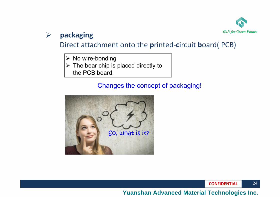
packaging Direct attachment onto the printed-circuit board( PCB)
Changes the concept of packaging!
No wire-bonding The bear chip is placed directly to
the PCB board.
So, what is it?
Yuanshan Advanced Material Technologies Inc.
GaN for Green Future
CONFIDENTIAL 25
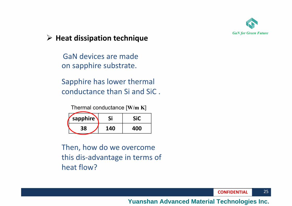
Heat dissipation technique
Sapphire has lower thermal conductance than Si and SiC .
sapphire Si SiC
38 140 400
Thermal conductance [W/m K]
Then, how do we overcome this dis-advantage in terms of heat flow?
GaN devices are made on sapphire substrate.
Yuanshan Advanced Material Technologies Inc.
GaN for Green Future
CONFIDENTIAL
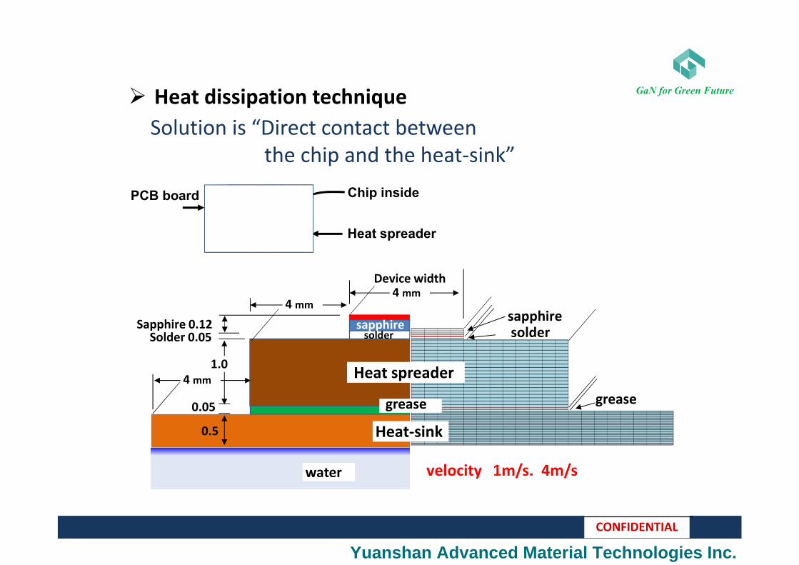
Heat dissipation technique
Solution is “Direct contact between the chip and the heat-sink”
Heat spreader
0.5
Solder 0.05
1.0
0.05
Sapphire 0.12
4 mm4 mm
grease
soldersapphire
velocity 1m/s. 4m/s
4 mm
water
Heat spreader
Heat-sink
sapphire
grease
Device width
solder
Chip insidePCB board
Yuanshan Advanced Material Technologies Inc.
GaN for Green Future
CONFIDENTIAL
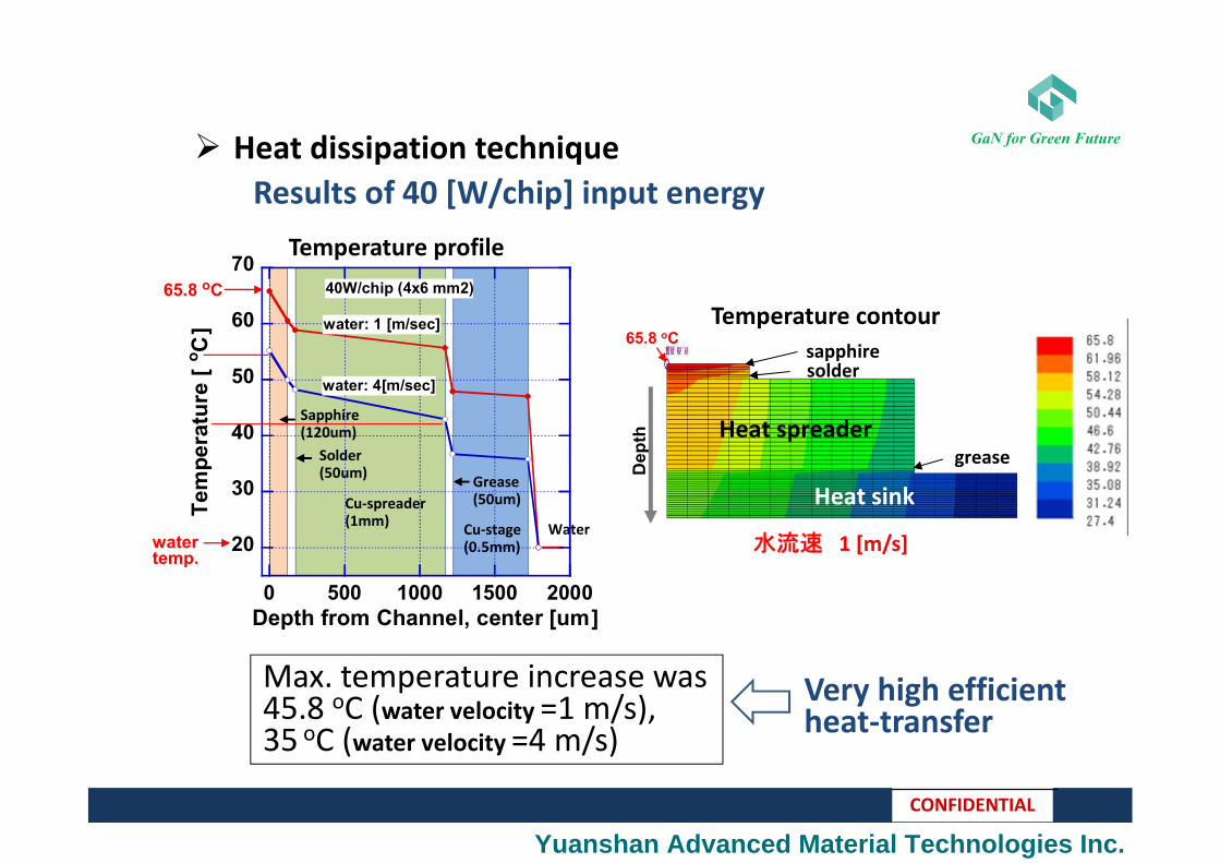
Cu-stage(0.5mm)
Sapphire(120um)
Grease(50um)Cu-spreader
(1mm)
Solder(50um)
Water 20
30
40
50
60
70
0 500 1000 1500 2000
40W/chip (4x6 mm2)
Tem
pera
ture
[ o
C ]
Depth from Channel, center [ um ]
water: 1 [m/sec]
water: 4[m/sec]
Temperature profile
Results of 40 [W/chip] input energy
grease
soldersapphire
水流速 1 [m/s]
Heat dissipation technique
Temperature contour
Dep
th
65.8 oC
65.8 oC
Max. temperature increase was 45.8 oC (water velocity =1 m/s), 35 oC (water velocity =4 m/s)
Very high efficient heat-transfer
Heat spreader
Heat sink
water temp.
Yuanshan Advanced Material Technologies Inc.
GaN for Green Future
CONFIDENTIAL 28
3
4
5
6
7
8
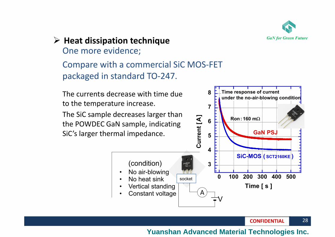
0 100 200 300 400 500
Time response of currentunder the no-air-blowing condition
Cu
rre
nt
[ A ]
Time [ s ]
Ron : 160 m
GaN PSJ
SiC-MOS ( SCT2160KE )
Heat dissipation techniqueOne more evidence;
Compare with a commercial SiC MOS-FET packaged in standard TO-247.
A
socket
V
• No air-blowing• No heat sink• Vertical standing• Constant voltage
The currents decrease with time due to the temperature increase.
The SiC sample decreases larger than the POWDEC GaN sample, indicating SiC’s larger thermal impedance.
(condition)
Yuanshan Advanced Material Technologies Inc.
GaN for Green Future
CONFIDENTIAL 29
Summary
Today’s main stream GaN power technology,(Field-plate GaN-FET on Si substrate) is being encountered sever challenges in terms of high-voltage and mass-productivity.
GaN PSJ technology platform has a
potential to replace the present Silicon counterparts due not only to the performance but also the production cost.
謝謝
Yuanshan Advanced Material Technologies Inc.
Related Documents