SPECIFICATIONS Delivering the market’s cleanest signal integrity at 28+ Gbps, Molex’s modular NeoScale™ Mezzanine System features a high-speed triad wafer design with Solder-Charge Technology™ for customized PCB routing in high-density system applications Ideal for space-constrained designs with limited PCB real estate, the modular NeoScale mezzanine system provides a durable and easily customizable design tool for high-density system applications. Each NeoScale triad wafer is an independent element in the housing and can be customized to a design layout. With four triad wafer configurations, customers can mix and match components to build a mezzanine solution to meet their requirements for signals supporting high-speed differential pairs (85 and 100 ohm), high-speed single-ended transmissions, low- speed single-ended signals and power contacts. For more information visit: www.molex.com/link/neoscale.html. NeoScale™ High-Speed Mezzanine System 170807 Vertical Plug 170814 Vertical Receptacle FEATURES AND BENEFITS NeoScale™ High-Speed Mezzanine System Left: Plug, Right: Receptacle 6-by-20 (120 triads) • Patent-pending modular triad wafer design with four triad configurations and high-speed differential pairs (in both 85 and 100 Ohm impedance), high-speed single-ended traces, low- speed single-ended lines and power contacts provides a customized system for design flexibility • Housing design based on honeycomb construction isolates each differential pair for optimal performance and customization • High-speed triad wafers comprise three pins per differential pair (two signal pins and one shielded ground pin) providing stand-alone 28+ Gbps fully shielded differential pairs with dedicated grounds • Connectors feature 246 circuits with a density of 82 differential pairs per square inch offers ultra-high-density signal solution with optimal signal integrity performance • Mirror-image triad layout enables the PCB routing in one or two layers for four- and six-row housings respectively providing ease in PCB routing and lowers overall system costs by decreasing the number of PCB layers required for signal routing • Tombstone structures incorporated within the receptacle housing prevents terminal damage by protecting the mating contact interface • Innovative PCB connection using patented Solder-Charge Technology™; proven surface mount technology (SMT) attach method for highly reliable and robust solder joints • Available in 12.00 to 42.00mm stack heights, circuit sizes of 8 to 300 triad wafers in 2-, 4-, 6-, 8- and 10-rows and 85 or 100 Ohm impedance provides design flexibility to address engineering constraints in system envelopes • Reliable mating interface with 2.00mm wipe gives sufficient conductive wipe for clean signal transmission and enhanced performance • Durable housing material provides a robust system with mechanical stability Reference Information Packaging: Tray Mates With: NeoScale Vertical Plug (Series 170807) mates with NeoScale Vertical Receptacle (Series 170814) Designed In: Millimeters RoHS: Yes Halogen Free: Yes Electrical Voltage (max.): 30V AC RMS max. Current (max.): 1.0A Contact Resistance: 30 Milliohms max. Dielectric Withstanding Voltage: 200V AC RMS Insulation Resistance: 1000 Megohms min. Mechanical Contact Retention to Housing: 1N Mating Force: 0.75N max. Unmating Force: 0.25N min. Durability (min.): 100 cycles Physical Housing: High-temperature LCP Contact: Copper (Cu) Plating: Contact Area — 30µ" Gold (Au) Solder Tail Area —15µ" Gold (Au) Underplating — 45µ" Nickel (Ni) Operating Temperature: -55 to +85°C

Welcome message from author
This document is posted to help you gain knowledge. Please leave a comment to let me know what you think about it! Share it to your friends and learn new things together.
Transcript

SPECIFICATIONS
Delivering the market’s cleanest signal integrity at 28+ Gbps, Molex’s modular NeoScale™ Mezzanine System features a high-speed triad wafer design with Solder-Charge Technology™ for customized PCB routing in high-density system applications
Ideal for space-constrained designs with limited PCB real estate, the modular NeoScale mezzanine system provides a durable and easily customizable design tool for high-density system applications. Each NeoScale triad wafer is an independent element in the housing and can be customized to a design layout. With four triad wafer configurations, customers can mix and match components to build a mezzanine solution to meet their requirements for signals supporting high-speed differential pairs (85 and 100 ohm), high-speed single-ended transmissions, low-speed single-ended signals and power contacts.
For more information visit: www.molex.com/link/neoscale.html.
NeoScale™ High-Speed Mezzanine System170807 Vertical Plug170814 Vertical Receptacle
FEATURES AND BENEFITS
NeoScale™ High-Speed Mezzanine System Left: Plug, Right: Receptacle
6-by-20 (120 triads)
• Patent-pending modular triad wafer design with four triad configurations and high-speed differential pairs (in both 85 and 100 Ohm impedance), high-speed single-ended traces, low-speed single-ended lines and power contacts provides a customized system for design flexibility
• Housing design based on honeycomb construction isolates each differential pair for optimal performance and customization
• High-speed triad wafers comprise three pins per differential pair (two signal pins and one shielded ground pin) providing stand-alone 28+ Gbps fully shielded differential pairs with dedicated grounds
• Connectors feature 246 circuits with a density of 82 differential pairs per square inch offers ultra-high-density signal solution with optimal signal integrity performance
• Mirror-image triad layout enables the PCB routing in one or two layers for four- and six-row housings respectively providing ease in PCB routing and lowers overall system costs by decreasing the number of PCB layers required for signal routing
• Tombstone structures incorporated within the receptacle housing prevents terminal damage by protecting the mating contact interface
• Innovative PCB connection using patented Solder-Charge Technology™; proven surface mount technology (SMT) attach method for highly reliable and robust solder joints
• Available in 12.00 to 42.00mm stack heights, circuit sizes of 8 to 300 triad wafers in 2-, 4-, 6-, 8- and 10-rows and 85 or 100 Ohm impedance provides design flexibility to address engineering constraints in system envelopes
• Reliable mating interface with 2.00mm wipe gives sufficient conductive wipe for clean signal transmission and enhanced performance
• Durable housing material provides a robust system with mechanical stability
Reference InformationPackaging: Tray
Mates With: NeoScale Vertical Plug (Series
170807) mates with NeoScale Vertical Receptacle (Series 170814)
Designed In: Millimeters
RoHS: Yes
Halogen Free: Yes
ElectricalVoltage (max.): 30V AC RMS max.
Current (max.): 1.0A
Contact Resistance: 30 Milliohms max.
Dielectric Withstanding Voltage: 200V AC RMS
Insulation Resistance: 1000 Megohms min.
MechanicalContact Retention to Housing: 1N
Mating Force: 0.75N max.
Unmating Force: 0.25N min.
Durability (min.): 100 cycles
PhysicalHousing: High-temperature LCP
Contact: Copper (Cu)
Plating: Contact Area — 30µ" Gold (Au) Solder Tail Area —15µ" Gold (Au) Underplating — 45µ" Nickel (Ni)
Operating Temperature: -55 to +85°C
ADDITIONAL PRODUCT FEATURES
APPLICATIONS
ORDERING INFORMATION
Plug
Order No. Plating Connector HeightTriad Wafer Configuration
(row-by-column)
170807-001130µ" Gold
8.00mm 4-by-18
170807-0015 12.00mm 6-by-8
Receptacle
Order No. Plating Connector HeightTriad Wafer Configuration
(row-by-column)
170814-000930µ" Gold
8.00mm 4-by-18
170814-0015 12.00mm 6-by-8
www.molex.com/link/neoscale.html
Order No. 987650-6991 Rev. 0.1 Printed in USA/KC/2012.06 © 2012, Molex
NeoScale™ High-Speed Mezzanine System170807 Vertical Plug170814 Vertical Receptacle
• Plug assembly features one differential pair with a 2.80mm pitch
• Receptacle assembly housing includes polarization and keying features
• Ground pin has two SMT attachment points, with four solder charge joints per triad wafer
• The orientation of the NeoScale plug and receptacle provides a mirrored configuration with a dividing line of back-to-back shields. The resulting mirror line bisects the triad pair to facilitate PCB routing and RX/TX pin-out management for optimal signal integrity and mechanical stability.
Unique, patent-pending triad wafer design (individual
triad close-up)
Triad wafer configuration Dense mechanicalenvelope of mated
system
Honeycomb housing structure for improved
signal clarity
Tombstone feature inhousing to preventterminal damage
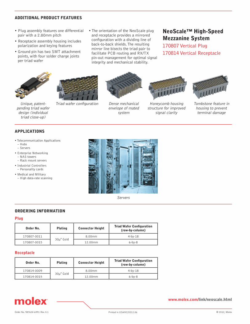
• Telecommunication Applications – Hubs – Servers
• Enterprise Networking – NAS towers – Rack mount servers
• Industrial Controllers – Personality cards
• Medical and Military – High data-rate scanning
Servers
Related Documents