Neo_WM620 WCDMA Module Hardware User Guide Version 1.4

Welcome message from author
This document is posted to help you gain knowledge. Please leave a comment to let me know what you think about it! Share it to your friends and learn new things together.
Transcript
Neo_WM620 WCDMA Module
Hardware User Guide
Version 1.4

Neo_M680 GPRS Module Hardware User Guide
Copyright © Neoway Technology Co., Ltd i
Copyright © Neoway Technology Co., Ltd 2014. All rights reserved.
No part of this document may be reproduced or transmitted in any form or by any means without prior
written consent of Shenzhen Neoway Technology Co., Ltd.
is the trademark of Neoway Technology Co., Ltd.
All other trademarks and trade names mentioned in this document are the property of their respective
holders.
Notice
This document is intended for system engineers (SEs), development engineers, and test engineers.
The information in this document is subject to change without notice due to product version update or
other reasons.
Every effort has been made in preparation of this document to ensure accuracy of the contents, but all
statements, information, and recommendations in this document do not constitute a warranty of any
kind, express or implied.
Neoway provides customers complete technical support. If you have any question, please contact
your account manager or email to the following email addresses:
Website: http://www.neoway.com.cn

Copyright © Neoway Technology Co., Ltd ii
Revision Record
Issue Changes Revised By Date
V1.0 Initial draft Tang Kefu 2013-09
V1.1 Added UART description Tang Kefu 2013-10
V1.2 Modified the description of the USB interfaces Tang Kefu 2013-12
V1.3 Modified the description of some pins Li Qiusheng 2014-02
V1.4 Adjusted the structure of this guide
Added sections 3.6 Sleep Mode and 3.8 RF
Interface, chapters 4 RF Features, and 5 Electric
Features and Reliability
Li Qiusheng
2014-06

Copyright © Neoway Technology Co., Ltd iii
Contents
1 Introduction to WM620 .................................................................................................... 1
1.1 Overview ..................................................................................................................................... 1
1.2 Block Diagram ............................................................................................................................ 1
1.3 Specifications .............................................................................................................................. 2
2 Pin Description and PCB Foot Print .............................................................................. 4
2.1 Specifications .............................................................................................................................. 4
2.2 Pin Definition .............................................................................................................................. 5
2.3 PCB Foot Print ............................................................................................................................ 7
3 Interface Design................................................................................................................. 8
3.1 Power Supply and Switch Interfaces ........................................................................................... 8
3.1.1 VBAT ................................................................................................................................. 8
3.1.2 VRTC ............................................................................................................................... 10
3.1.3 VDD ................................................................................................................................. 11
3.1.4 ON_OFF Pin and Power-on Procedure ............................................................................ 11
3.1.5 RESET .............................................................................................................................. 13
3.2 Running Status Indication ......................................................................................................... 14
3.2.1 LED Indicator ................................................................................................................... 14
3.2.2 RING Pin .......................................................................................................................... 15
3.3 USIM Card Interface ................................................................................................................. 15
3.4 USB Interfaces .......................................................................................................................... 17
3.5 UART ........................................................................................................................................ 18
3.5.1 Basic Descriptions of UART ............................................................................................ 18
3.5.2 Level Shifting for UART .................................................................................................. 20
3.6 Sleep Mode ................................................................................................................................ 21
3.6.1 UART Control .................................................................................................................. 21
3.6.2 USB Control ..................................................................................................................... 22
3.7 Audio Interface .......................................................................................................................... 23
3.8 RF Interface ............................................................................................................................... 25
3.8.1 RF Design and PCB Layout ............................................................................................. 25
4 RF Features ....................................................................................................................... 27
4.1 Work Band ................................................................................................................................. 27
4.2 Transmitting Power and Receiving Sensitivity ......................................................................... 27
4.2.1 Transmitting Power .......................................................................................................... 27
4.2.2 Receiving Sensitivity ........................................................................................................ 28
5 Electric Features and Reliability................................................................................... 29
5.1 Electric Feature ......................................................................................................................... 29
5.2 Temperature ............................................................................................................................... 29
5.3 Current....................................................................................................................................... 29

Copyright © Neoway Technology Co., Ltd iv
5.4 ESD Protection .......................................................................................................................... 31
6 Typical Circuits ................................................................................................................ 32
7 Mounting the Module onto the Application Board.................................................. 34
8 Package .............................................................................................................................. 34
9 Abbreviations ................................................................................................................... 35

Copyright © Neoway Technology Co., Ltd v
Table of Figures
Figure 2-1 Bottom view of the WM620 module...................................................................................... 4
Figure 2-2 PCB foot print recommended for WM620 (unit: mm) ........................................................... 7
Figure 3-1 Current peaks and voltage drops ............................................................................................ 8
Figure 3-2 Power supply design .............................................................................................................. 9
Figure 3-3 Reference design of power supply controlled by MIC29302 ................................................. 9
Figure 3-4 Reference design of power supply controlled by p-MOSFET ............................................. 10
Figure 3-5 RTC reference design ............................................................................................................11
Figure 3-6 Reference circuit of ON_OFF controlled by high level ....................................................... 12
Figure 3-7 Power-on procedure ............................................................................................................. 13
Figure 3-8 Reset circuit ......................................................................................................................... 13
Figure 3-9 LED indicator....................................................................................................................... 14
Figure 3-10 RING indicator for incoming call ...................................................................................... 15
Figure 3-11 RING indicator for SMS .................................................................................................... 15
Figure 3-12 Reference design of USIM card interface .......................................................................... 16
Figure 3-13 Recommended ESD diode array ........................................................................................ 16
Figure 3-14 Reference of SIM card socket ............................................................................................ 16
Figure 3-15 Reference USB circuit ....................................................................................................... 18
Figure 3-16 Signal connection between DCE and DTE ........................................................................ 19
Figure 3-17 Recommended circuit between 3.3V MCU and UART ..................................................... 20
Figure 3-18 Recommended circuit between 5V MCU and UART ........................................................ 20
Figure 3-19 Sleep mode controlled by UART ....................................................................................... 21
Figure 3-20 Sleep mode controlled by USB (a) ..................................................................................... 22
Figure 3-21 Sleep mode controlled by USB (b) .................................................................................... 22
Figure 3-22 Reference design of MIC differential connections ............................................................. 23
Figure 3-23 Reference design of single-end input MIC interface .......................................................... 24
Figure 3-24 Reference design for speaker differential output ............................................................... 24
Figure 3-25 Reference design for speaker single-ended output ............................................................. 24
Figure 3-26 Reference design for antenna interface .............................................................................. 26
Figure 3-27 RF layout reference ............................................................................................................ 26

Copyright © Neoway Technology Co., Ltd vi
Table of Tables
Table 1-1 WM620 specifications ............................................................................................................. 2
Table 2-1 WM620 pin definition ............................................................................................................. 5
Table 3-1 Power supply and switch interface .......................................................................................... 8
Table 3-2 Capacity matching power failure duration .............................................................................11
Table 3-3 LED indicator ........................................................................................................................ 14
Table 3-4 SIM Card Interface ................................................................................................................ 15
Table 3-5 USB interface ........................................................................................................................ 17
Table 3-6 UART .................................................................................................................................... 18
Table 3-7 Audio interface ...................................................................................................................... 23
Table 3-8 MIC voltage and current ........................................................................................................ 24
Table 3-9 EAR parameter ...................................................................................................................... 25
Table 3-10 SPK parameter ..................................................................................................................... 25
Table 4-1 Work band ............................................................................................................................. 27
Table 4-2 Transmitting power (unit: dBm) ............................................................................................ 27
Table 4-3 Receiving sensitivity (Unit: dBm) ......................................................................................... 28
Table 5-1 Electric feature of the module ............................................................................................... 29
Table 5-2 Temperature Feature (Unit: ºC) ............................................................................................. 29
Table 5-3 Operating current (Unit: mA) ................................................................................................ 30
Table 5-4 Current in sleep mode ............................................................................................................ 30
Table 5-5 ESD feature of the module .................................................................................................... 31

Neo_WM620 WCDMA Module Hardware User Guide
Copyright © Neoway Technology Co., Ltd 1
1 Introduction to WM620
1.1 Overview
WM620 is a WCDMA module that supports multiple network modes including HSDPA, UMTS, EDGE,
GPRS, and GSM. For HSDPA, this module supports 3.6 Mbit/s for downlink data and 384 Kbit/s for uplink
data. WM620 provides high-quality data and voice communication, SMS and other functions, and is widely
applied to electricity, Internet of Vehicle (IoV), video monitoring, handset devices, etc.
WM620 is an SMT module in LCC compact package. It can be easily adopted for standard Mini PCI-E
interface. WM620 includes the following product series.
Band
Model
UMTS 2100
UMTS 1900
UMTS 900
UMTS 850
PCS 1900
DCS 1800
EGSM 900
GSM 850
WM620-A √ √ √ √ √ √
WM620-B √ √ √ √ √ √
This user guide details the features, indicators, and testing standards of WM620.
1.2 Block Diagram
WM620 module consists of power supply management, baseband controller, MCP, power amplifier (PA),
19.2 MHz transistor, 32.768 KHz transistor, various application interfaces, etc. All sections coordinate
with each other to provide such communication functions as data and voice services.
The following figure shows the block diagram of WM620.

Neo_WM620 WCDMA Module Hardware User Guide
Copyright © Neoway Technology Co., Ltd 2
1.3 Specifications
Table 1-1 WM620 specifications
Specification Description
Frequency Band WM620-A: UMTS2100/900 MHz GSM850/900/1800/1900 MHz
WM620-B: UMTS1900/850 MHz GSM850/900/1800/1900 MHz
Sensitivity -107 dBm
Max. Transmit Power
GSM/GPRS 850M/900 MHz: +33 dBm (Power Class 4)
GSM/GPRS 1800 MHz/1900 MHz: +30 dBm (Power Class 1)
EDGE 850M/900 MHz: +27 dBm (Power Class E2)
EDGE1800 MHz/1900 MHz: +26 dBm (Power Class E2)
WCDMA/HSDPA: +23 dBm (Power Class 3)
Transient Current Max 2 A
Standby Current (Idle) <5.0 mA
Operating Temperature –30°C to + 80°C
Storage Temperature –40°C to + 85°C
Dimension 30 mm x 30 mm x 2.7 mm
Operating Voltage 3.3 V to 4.2 V DC (recommended 3.9 V, 25°C)
AT Command
GSM07.07
Neoway extended AT commands (Refer to Neo_WM620 WCDMA Module AT Command Set)
Driver Supporting Windows XP, Windows 7, Linux(2.6.1), Android
Audio GSM: FR, EFR, HR, AMR Voice Coding, DTMF
WCDMA: AMR, ARM-WB
SMS TEXT/PDU
Point of Point / Cell Broadcast
Technical Standard
UMTS/WCDMA/GSM/GPRS/EDGE Specification Release 99 (3GPP R99)
UMTS/WCDMA Specification Release 5 (3GPP R5)
HSDPA DL: 3.6 Mbit/s
GSM/GPRS/EDGE Specification Release 4 (3GPP R4)
GPRS/EDGE Multislot Class 12, Release 4
DTM Multislot Class 11
Data Rate
GSM CS: UL 14.4 Kbit/s / DL 14.4 Kbit/s
GPRS: UL 85.6 Kbit/s / DL 85.6 Kbit/s
EDGE: DL 236.8 Kbit/s / UL: 236.8 Kbit/s
WCDMA CS: UL 64 Kbit/s / DL 64 Kbit/s
WCDMA PS: UL 384 Kbit/s / DL 384 Kbit/s

Neo_WM620 WCDMA Module Hardware User Guide
Copyright © Neoway Technology Co., Ltd 3
HSDPA: DL 3.6 Mbit/s / UL 384 Kbit/s
Circuit Switched Data Support CSD
Support USSD
Supplementary Service
Call Transfer (CFB, CFNA, CFU)
Call Waiting
Three-Way Calling

Neo_WM620 WCDMA Module Hardware User Guide
Copyright © Neoway Technology Co., Ltd 4
2 Pin Description and PCB Foot Print
2.1 Specifications
Specifications WM620
Dimensions 30 mm x 30 mm x 2.7 mm (H x W x D)
Weight 5 g
Encapsulation 62-pin LGA
Figure 2-1 Bottom view of the WM620 module
MIC
_1P
SPK_N
RE
SE
T
V_B
US
US
IM _
CL
K
TX
D
RIN
G
ANT_M
SPK_P
MIC
_1N
EA
R_N
EA
R_P
VD
D_2
.6V
VD
D_1
.8V
VB
AT
VB
AT
US
B_D
-
US
B_D
+
US
IM _
DA
TA
US
IM _
RS
T
US
IM_
VC
C
SL
EE
P_IN
RX
D
RT
S
CT
S
SIG
_L
ED
ON
_O
FF
POWER
GND
USB Audio UIM UART Reserved
JTAG RF_ANT Empty
VR
TC
MIC_2P
MIC_2N
AD
C
Others

Neo_WM620 WCDMA Module Hardware User Guide
Copyright © Neoway Technology Co., Ltd 5
The figure shows main application pins. Select pins based on your product requirements and
leave pins that you do not use not connected.
For more details about pins, see the pin description.
JTAG pins have not be open to customers.
2.2 Pin Definition
Table 2-1 WM620 pin definition
Pin No. Pin Name I/O Function Level Feature (V)
Remarks
Power Supply and Switch Interfaces
22, 23 VBAT PWR Main power supply 3.3 V to 4.2 V
26 VDD_1.8V PWR 1.8 V power supply
output Continuous voltage
output after the
module is on 27 VDD_2.6V PWR 2.6 V power supply
output
47 VRTC PWR RTC power supply I/O 1.5 V to 3.25 V DC
Typical value: 3.0 V
46 ON_OFF I On/Off control Internally pulled up
to 1.8 V by 200K
25 RESET DI Reset pin VDD_1.8V
1, 12, 17,
21, 24,
34, 43,
45, 50, 61
GND PWR Ground
Audio Interface
28 EAR_P AO Earphone amplifier
output (+)
Keep not connected
(NC) if not used 29 EAR_N AO
Earphone amplifier
output (-)
30 MIC_1N AI Microphone #1 input (-)
Keep NC if not used
31 MIC_1P AI Microphone #1 input (+)
32 MIC_2P AI Microphone #2 input (-)
Keep NC if not used
33 MIC_2N AI Microphone #2 input (+)
35 SPK_P AO Speaker amplifier output
(+) Keep NC if not used
36 SPK_N AO Speaker amplifier output
(-) Keep NC if not used
UART Interface

Neo_WM620 WCDMA Module Hardware User Guide
Copyright © Neoway Technology Co., Ltd 6
52 CTS I UART to send data VDD_2.6V
At most 3 V input
Not support
firmware update
53 RTS O UART ready for receiving
data VDD_2.6V
54 RXD I High-speed UART
receive data input VDD_2.6V
55 TXD O High-speed UART
transmit data output VDD_2.6V
SIM Card
13 USIM_VCC PWR USIM card power supply 1.8V/3V
14 USIM_RST O USIM card reset 1.8V/3V
15 USIM_DATA I/O USIM card data 1.8V/3V
Externally pulled up
to USIM_VCC by
10K
16 USIM _CLK I/O USIM card clock 1.8V/3V
USB Interfaces
18 USB_D+ I/O High-speed USB
differential USB data (+)
Used for firmware
updating 19 USB_D- I/O
High-speed USB
differential USB data (-)
20 V_BUS PWR USB power supply Voltage range: 3.3 V
to 5.25 V
Antenna
44 ANT_M AI/AO RF I/O
LED Indicator
48 SIG_LED O Network indicator VDD_2.6V
SMS and Incoming Call Ring
51 RING O Indicating an incoming
call or message VDD_2.6V
Sleep Mode Controlling
60 SLEEP_IN DI Controlling the sleep
mode VDD_1.8V
ADC
49 ADC AI 12-bit ADC input Voltage range: 0 V
to 2.2 V
Reserved Pins
2-11,
37-42,
56-59, 62 NC
NC

Neo_WM620 WCDMA Module Hardware User Guide
Copyright © Neoway Technology Co., Ltd 7
2.3 PCB Foot Print
LGA packaging is adopted to package the pins of the WM620 module. Figure 2-2 shows the recommended
PCB foot print.
Figure 2-2 PCB foot print recommended for WM620 (unit: mm)

Neo_WM620 WCDMA Module Hardware User Guide
Copyright © Neoway Technology Co., Ltd 8
3 Interface Design
3.1 Power Supply and Switch Interfaces
Table 3-1 Power supply and switch interface
Pin Name I/O Function Remarks
22, 23 VBAT PWR Main power supply 3.3 V to 4.2 V (3.9 V is recommended)
26 VDD_1.8V PWR 1.8 V power supply output
27 VDD_2.6V PWR 2.6 V power supply output
47 VRTC PWR RTC power supply input/output Not used for any other functions
Ensure that the VBAT never exceeds 4.5 V DC. Voltage higher than 4.5 V DC may damage the WM620
module.
3.1.1 VBAT
VBAT is the main power supply of the module. Its input voltage ranges from 3.3 V to 4.2 V and the
preferable value is 3.9V. The average current is lower than 500 mA. In addition to digital signals and analog
signals, it supplies power for RF power amplifier.
The performance of the VBAT power supply is a critical path to module's performance and stability. The
peak input current at the VBAT pin can be up to 2 A when the signal is weak and the module works at the
maximum transmitting power. The voltage will encounter a drop in such a situation. The module might
restart if the voltage drops lower than 3.3 V. Thus a large capacitor (e.g. 100 μF tantalum capacitor or 470
μF aluminum capacitor) with low ESR must be installed near the VBAT to avoid or reduce the voltage drop
caused by the RF power amplifier. Figure 3-1 shows the burst current and the voltage drops.
Figure 3-1 Current peaks and voltage drops
Keep above 3.3 V3.3 V
0 ms 3.7 ms 7.4 ms 10.7 ms T
2 A
Voltage
Input
Current
3.9 V

Neo_WM620 WCDMA Module Hardware User Guide
Copyright © Neoway Technology Co., Ltd 9
Figure 3-2 shows a recommended power supply design for the module.
Figure 3-2 Power supply design
The current test results vary with the internal impedance of the ESR capacitors and power supply. In the
above circuit, you can use TVS diode at D1 to enhance the performance of the module during a burst. A 100
μF capacitor with low ESR or 470 μF aluminum capacitor is expected at C1 to reduce voltage drops during
bursts. In case of Li-ion cell battery used, a 220 μF tantalum capacitor may be applicable because the battery
has low internal impedance. In addition, you need to add 0.1 μF, 100 pF, and 33 pF filter capacitors to filter
high frequency interference.
A controllable power supply is preferable if the module is used in harsh conditions. The WM620 module
might fail to reset in remote or unattended applications, or in an environment with great electromagnetic
interference (EMI). You can use the EN pin on the LDO or DC/DC chipset to control the power supply as
shown in Figure 3-3 if you adopt 5 V power supply.
MIC29302WU in the following figure is an LDO and it can output 3 A current to ensure the performance
of the module.
Figure 3-3 Reference design of power supply controlled by MIC29302
The alternative way is to use a p-MOSFET to control the module's power supply, as shown in Figure 3-4.
This way is used if the power supply system does not consist of an EN pin. When the MCU detects the exceptions such as no response from the module or GPRS disconnection, power-off/on can rectify the
module exceptions thoroughly. In Figure 3-4, the module is powered on when VCC_EN is set to high level.
Power Supply WM620
Close to the pins
D1 C1 C2 C3 C4
VBAT
Current testing
point
I_max
C1 I_max
10uF
100uF
470uF
1000uF
2A
1.1A
0.8A
0.6A
VCCIN
VCC_EN VCC_MAIN
100uF
TAN0.1uF
TVS
5V
0.1uF470uF
TAN
EN
VIN
VOUT
ADJ
MIC29302WU 10K
4.75KC1 C2
R1
R2
C3 C4 T1
Neo_WM620 WCDMA Module Hardware User Guide
Copyright © Neoway Technology Co., Ltd 10
Figure 3-4 Reference design of power supply controlled by p-MOSFET
VDD_3.9V VBAT
10K
100K TVS
5V
33 pF10 uF470 uF
VCC_EN 2K
10K
0.1 uF
Q1
Q2
R4C1 C2 C3 C4 C5 C6
R1
10 uF 0.1 uF
R3
INPUT OUTPUT
D1 +
R2
In the above circuit, Q2 is added to eliminate the need for a high enough voltage level of the host GPIO. In
case that the GPIO can output a high voltage greater than VDD_3.9V - |VGS(th)|, where VGS(th) is the Gate
Threshold Voltage, Q2 is not needed.
Reference components:
Q1 can be IRML6401 or Rds(on) p-MOSFET which has higher withstand voltage and drain current.
Q2: a common NPN transistor, e.g. MMBT3904; or a digital NPN transistor, e.g. DTC123. If digital
transistor is used, delete R1 and R2.
C4: 100 μF tantalum capacitor rated at 6.3V; or 470 μF aluminum capacitor.
Protection
It is strongly recommended that you add a TVS diode (VRWM=5 V) to the VBAT power supply. For some
stable power supplies, zener diodes can decrease the power supply overshoot. SMAJ5.0A/C, SMBJ5.0A/C,
MMSZ5231B1T1G from ONSEMI, and PZ3D4V2 from Prisemi are options.
Trace
The primary loop lines for VBAT on PCB must support the safe transmission of 2 A current and ensure no
obvious loop voltage decrease. Therefore, the trace width is required greater than 1.5 mm and the ground
should be as complete as possible.
3.1.2 VRTC
VRTC is the power supply pin of RTC inside the module to ensure that the clock works properly even
though the module encounters exceptional power failure. It can be connected to external battery or
supercapacitor. When VBAT works properly, VRTC outputs 2 mA current to charge the backup battery or
the capacitor. When VBAT is disconnected, the battery or capacitor will supply power for RTC in short time.
If you use a capacitor rather than a backup battery, connect the capacitor to the VRTC and then ground the capacitor. The capacitor must be charged before it supplies power for RTC in an exceptional situation.

Neo_WM620 WCDMA Module Hardware User Guide
Copyright © Neoway Technology Co., Ltd 11
Figure 3-5 shows the reference design of the VRTC power supply.
Figure 3-5 RTC reference design
The capacity of the supercapacitor is dependent on the duration of exceptional power failures. Table 3-2
shows the capacity matching the power failure duration.
Table 3-2 Capacity matching power failure duration
Power Failure Duration Capacity Encapsulation (X7R)
0.5 s 1.5 µF 0805
1.0 s 3.3 µF 0805
1.5 s 4.7 µF 0805
2.0 s 6.8 µF 1206
3.1.3 VDD
VDD_1.8V and VDD_2.6V are two power supply output pins, which can bear 20 mA in normal situation. It
is recommended that you use them only for level shifting. These two pins do not stop output after the
module enters the sleep mode.
3.1.4 ON_OFF Pin and Power-on Procedure
Prior to turning on the module, start the host MCU and complete the UART initialization. Otherwise
conflictions may occur during initialization due to unstable conditions.
ON/OFF is a low level pulse active input, used to turn on or off the module. It is pulled up to 1.8V internally
by a 200KΩ resistor and controlled by external OC. Figure 3-7 shows its pulse width and power-on
procedure.
When the WM620 is powered on, the VDD_2.6V pin will be pulled up and keep 2.6 V DC output. The
UART will send +EIND:8 after the module is powered on properly and send +EUSIM:1 after the USIM
card is identified. Then the module is ready to response AT commands. If the module does not identify the
USIM card, the UART will send +EIND:8+EUSIM:ERROR.
Backup
Battery
WM620
RTC
Circuit
2K
Capacitor
VRTCR1
C1
Neo_WM620 WCDMA Module Hardware User Guide
Copyright © Neoway Technology Co., Ltd 12
While the module is on, keep the ON_OFF pin low level for 2 seconds. Then the module enters shutdown
procedure and will be off in 5 seconds. Another approach to turn off the module is using AT commands.
For details, see Neo_WM620 WCDMA Module AT Command.
Keep ON_OFF low level or connecting to GND, and WM620 can start automatically when it is powered
on.
Figure 3-6 shows the circuit of ON_OFF controlled by high level pulse.
Figure 3-6 Reference circuit of ON_OFF controlled by high level
The ON_OFF pin might encounter pulse interference generated by ESD. It is recommended that you
parallel a 10 nF capacitor connected to the ground to protect the ON_OFF pin.
It is not recommended that you connect the ON_OFF pin to ground to start the module because it will
affect the ESD feature of the module.
The ON_OFF pin can control the module startup and shutdown. Do not repeat triggering this pin.
Otherwise, the startup or shutdown might fail. For example, the user plans to start up the module but gives
low level pulse for twice, resulting in shutdown.
The shutdown function of the ON_OFF pin is controlled by the software. If the software is not running
properly, the module cannot shut down properly.
Figure 3-7 shows the power-on procedure of the WM620 module.
WM620
ON_OFF
2K
10K
VT2
MCU ON_OFF 10 nF
C3
C3 is close to the pin.

Neo_WM620 WCDMA Module Hardware User Guide
Copyright © Neoway Technology Co., Ltd 13
Figure 3-7 Power-on procedure
3.1.5 RESET
RESET is a hard reset input pin that is pulled up internally by a resistance and activated by low level signal.
Low level pulse longer than 20 ms can reset the WM620 module. After resetting the module, you must
power on the module again. The recommended reset pulse is 50 ms, and cannot exceed 2 seconds.
Otherwise, the WM620 module will be powered off.
If you keep the ON_OFF pin low level or connecting to GND, the WM620 can restart automatically once
you reset the module. Figure 3-8 shows the reference design of reset circuit.
Figure 3-8 Reset circuit
The RESET pin is sensitive to pulse. Place a 10 nF filter capacitor close to the pin to filter natural
interference. Ensure complete ground around the trace of this pin and dig holes on both side of the trace.
If the level from the external MCU exceeds 1.8 V, OC control is recommended. Leave the pin not
connected if you do not use it.
VBAT
ON_OFF
RESET_N
0.5s<t<1s 1.6V<VH
VL<0.5V
USB_DP
2.5s<t<5s
Power-on
Procedure
Power-off
Procedure
4s 4.6s
VT2
MCU RESET 10nF
C3
R6 and C3 are close to the pin.
R5
R6
R6
100
WM620
RESET
10K
2K

Neo_WM620 WCDMA Module Hardware User Guide
Copyright © Neoway Technology Co., Ltd 14
The module works in complicated environment. It might encounter halt or other abnormities. Therefore,
you must take automatic restore into consideration when designing your products. The following two
methods are recommended:
Control the RESET pin (emergency shutdown) so that you can set low level for hard shutdown.
Perform the soft shutdown process by referring to Neo_WM620 WCDMA Module AT Command Set.
Five seconds later, power off or reset the module. Otherwise, the program might be damaged during
the hard shutdown if the module is reading or writing information in the memory.
3.2 Running Status Indication
3.2.1 LED Indicator
Table 3-3 LED indicator
Pin Name I/O Function Remarks
SIG_LED O Indicates running status Min Typical Max
-0.3 2.6 2.9
When the module is running, the LED indicator is driven by the SIG_LED to indicate different running
status with its various blink behaviors. For details, see Neo_WM620 WCDMA Module AT Command Set.
Module Status LED Status
1 Have registered 2G network and been idle Blink (500ms ON / 1500ms OFF)
2 Have registered 3G network and been idle Blink (100ms ON / 2900ms OFF)
3 Searching networks Blink twice (100 ms ON/100 ms OFF/100 ms
ON/2700 ms OFF)
4 Service (Voice or data) Blink (125ms ON /125ms OFF)
The LED can be directly connected to this pin with a resistor in series. For better luminance, drive the LED
with a transistor instead. The LED's brightness depends on the value of R1 and VCC.
Figure 3-9 LED indicator
SIG_LED
WM620 1K
SIG_LED
WM62010K
VCC
470
2K
R1

Neo_WM620 WCDMA Module Hardware User Guide
Copyright © Neoway Technology Co., Ltd 15
3.2.2 RING Pin
PIN Name I/O Function DC Characteristics (V)
51 RING O Ring output Min Typical Max
-0.3 2.6 2.9
Calling: Once a voice call is coming, UART output "RING" character strings and meanwhile the
RING pin outputs 250 ms low level pulses at 4s period. After the call is answered, the high level
restores.
Figure 3-10 RING indicator for incoming call
SMS: Upon receipt of SMS, the module outputs one 600 ms low level pulse.
Figure 3-11 RING indicator for SMS
You can change the pulse periods via AT commands. For details, see Neo_WM620 WCDMA Module
AT Command Set.
3.3 USIM Card Interface
Table 3-4 SIM Card Interface
PIN Name I/O Function Remarks
13 V_SIM PWR SIM card power output 1.8/3.0 V
14 SIM_RST DO SIM card clock output 1.8/3.0 V
15 SIM_DATA DO SIM card reset output 1.8/3.0 V
16 SIM_CLK I/O SIM card data input/output 1.8/3.0 V
250ms 250ms
4S
600 ms

Neo_WM620 WCDMA Module Hardware User Guide
Copyright © Neoway Technology Co., Ltd 16
WM620 supports 3.0 V and 1.8 V USIM cards. USIM_DATA need to be externally pulled up to
USIM_VCC by a 10 KΩ resistor. USIM_CLK works at 3.25MHz typically.
Figure 3-12 Reference design of USIM card interface
Figure 3-12 shows reference circuit design of the USIM card. ESD protectors, such as ESD diodes (lower
than 33 pF) or ESD varistors, are recommended on the USIM signals, especially in automotive electronics
or other applications with badly ESD. In Figure 3-12, T1 to T4 should be placed close to the USIM socket.
In other applications, replace ESD diodes with 22 pF to 33 pF grounding capacitors. The total distributed
capacitance, including the junction capacitance of the ESD diode or other devices, cannot be greater than
120 pF.
Figure 3-13 Recommended ESD diode array
If you use 6-pin SIM card sockets, MCP-C713(H2.8) is recommended. Figure 3-14 shows its
encapsulation.
Figure 3-14 Reference of SIM card socket
20
20
20
1 uF
USIM_DATA
USIM_CLK
USIM_RST
USIM_VCC
WM620
CLK
RST
VCC
VPP
GND
DATA
T1 T2 T3 T4C1
10K
USIM Card
L1
GND
L2
L3
L4
1
2
3
4
5
USIM_RST
USIM_CLK
USIM_DATA
USIM_VCC

Neo_WM620 WCDMA Module Hardware User Guide
Copyright © Neoway Technology Co., Ltd 17
The pins of USIM card socket:
Pin 1 USIM_CLK
Pin 2 USIM_ DATA
Pin 3 USIM_RST
Pin 4 USIM_VPP
Pin 5 USIM_VCC
Pin 6 GND
USIM signal is sensitive to GSM TDD noise and RF interference. So, the PCB design should meet the
following requirements:
Avoid bifurcation at PCB trace of SIM_CLK.
Ensure as short PCB traces of USIM_DATA and USIM CLK as possible and surround the traces
with GND copper.
RF traces or RF connector should be far away from the USIM card and USIM card traces.
Ensure that the USIM traces are as smooth as possible.
Place ESD diodes or filter capacitors close to the USIM card.
3.4 USB Interfaces
Table 3-5 USB interface
Pin Signal I/O Function Remarks
18 USB D+ I/O High-speed USB differential data, (+)
19 USB D- I/O High-speed USB differential data, (-)
20 V_USB PWR USB Power Input voltage 3.3 to 5.5 V.
The WM620 module is compliant with USB 2.0 full speed device. The USB 2.0 specification requires that
the hosts such as computers support three USB speeds: low-speed (1.5 Mbit/s), full-speed (12 Mbit/s) and
high-speed (480 Mbit/s).
The V_USB pin is a USB power supply input. Parallel ESD diodes respectively close to the three signals.
The following circuit between the module and a computer is recommended.

Neo_WM620 WCDMA Module Hardware User Guide
Copyright © Neoway Technology Co., Ltd 18
Figure 3-15 Reference USB circuit
The USB circuit design should comply with the USB 2.0.
The traces of USB_D+ and USB_D- must be routed as a group of differential pair with 90 Ω differential
impedance.
The USB differential pair should be routed side-by-side and on the same layer.
USB_D+ and USB_D- is a pair of high speed signals, so the trace lengths should match as well as
possible.
USB interface must be connected or set aside the relevant test points to facilitate subsequent firmware
upgrade or debugging.
3.5 UART
Table 3-6 UART
Pin Signal I/O Function Remarks
52 CTS I High-speed UART to send data
53 RTS O High-speed UART ready for receiving data
54 RXD I High-speed UART receive data input (allow 3 V input at most)
55 TXD O High-speed UART transmit data output
3.5.1 Basic Descriptions of UART
UART is used for AT commands, data sending/receiving, etc.
DCE
V_USB
USB_D
USB_D+
GND
DTE
UTXD
URXD
RTS
CTS
VBUS
USB_DM
USB_DP
GND
20
20
Neo_WM620 WCDMA Module Hardware User Guide
Copyright © Neoway Technology Co., Ltd 19
The UART of WM620 works at 2.6 V CMOS logic level. The voltages for input high level should not
exceed 3.0 V. Supported baud rates are 300, 600, 1200, 2400, 4800, 9600, 14400, 19200, 38400, 57600,
115200, 230400, 460800, 921600 bit/s, and the default rate is 115200 bit/s.
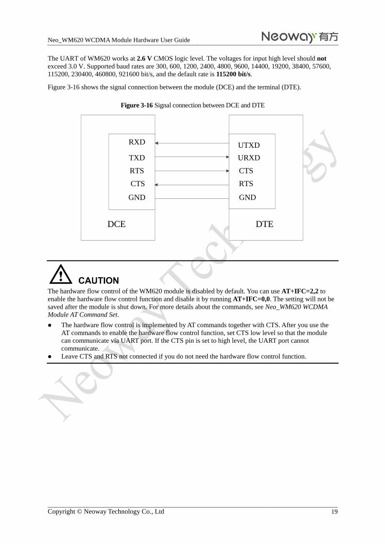
Figure 3-16 shows the signal connection between the module (DCE) and the terminal (DTE).
Figure 3-16 Signal connection between DCE and DTE
The hardware flow control of the WM620 module is disabled by default. You can use AT+IFC=2,2 to
enable the hardware flow control function and disable it by running AT+IFC=0,0. The setting will not be
saved after the module is shut down. For more details about the commands, see Neo_WM620 WCDMA Module AT Command Set.
The hardware flow control is implemented by AT commands together with CTS. After you use the
AT commands to enable the hardware flow control function, set CTS low level so that the module
can communicate via UART port. If the CTS pin is set to high level, the UART port cannot
communicate.
Leave CTS and RTS not connected if you do not need the hardware flow control function.
RXD
TXD
RTS
CTS
UTXD
URXD
CTS
RTS
GND GND
DTEDCE

Neo_WM620 WCDMA Module Hardware User Guide
Copyright © Neoway Technology Co., Ltd 20
3.5.2 Level Shifting for UART
If the UART is interfacing with a MCU that has 3.3 V logic levels, a resistor should be connected in series
with the signals.
Figure 3-17 Recommended circuit between 3.3V MCU and UART
If the UART is interfaced with an MCU that has 5 V logic levels, level shifting is required for both UART
receive and transmit. Figure 3-18 shows a reference circuit.
Figure 3-18 Recommended circuit between 5V MCU and UART
Reference components:
R2: 2K-10K. The higher rate the UART works at, the smaller value used.
R3: 4.7K-10K. The higher rate the UART works at, the smaller value used.
Q1: MMBT3904 or MMBT2222. High-speed transistors are preferred.
Logic level: DTE 5 V—>DCE 2.6 V
200
33 pF
33 pF
MCU_UTXD
MCU_URXD
RXD
TXD
200
OUTPUT
VCC_IN VCC_OUT
4.7K 10KR2 R3
INPUT Q1

Neo_WM620 WCDMA Module Hardware User Guide
Copyright © Neoway Technology Co., Ltd 21
INPUT is connected to TXD of the MCU and VCC_IN is connected to the 5 V power supply of the external
device. OUTPUT is connected to RXD of the module and VCC_OUT is connected to VDD_2.6V of the
module.
Level shifting between RXD of the MCU and TXD of the module can be implemented in the same way.
This design can be also used for RING.
Avoid spark or fault on UART during the power-on procedure of the module.
Do not send any data to UART within 5 seconds after the module is turned on.
3.6 Sleep Mode
The sleep mode of WM620 is controlled in two ways: UART and USB. The module can receive voice and
SMS message in sleep mode controlled by UART or USB. Upon receiving SMS messages, voice, or data,
the module is woken up automatically. Then you can execute AT commands and the module will enter the
sleep mode after the service is end.
3.6.1 UART Control
If the module (DCE) communicate with DTE via UART, connect them as shown in Figure 3-19 to control
the sleep mode. SLEEP_IN controls the status of the sleep mode and can be used to wake up the module
from the sleep mode.
Figure 3-19 Sleep mode controlled by UART
When the V_BUS pin of USB is not connected, send AT+ENPWRSAVE=0 via UART to allow the
module to enter the sleep mode. If the SLEEP_IN pin is set to low level, the module enters sleep mode;
if SLEEP_IN is set to high level, the module is woken up.
To disable the sleep mode, execute AT+ENPWRSAVE=1. Then, the module will never enter the
sleep mode.
RXD
TXD
RTS
CTS
UTXD
URXD
CTS
RTS
GND GND
DTEDCE
SLEEP_IN GPIO

Neo_WM620 WCDMA Module Hardware User Guide
Copyright © Neoway Technology Co., Ltd 22
3.6.2 USB Control
If the module (DCE) communicates with DTE via USB port, the following two methods are
recommended to bring the module into the sleep mode.
1. When the DTE supports the Suspend state of USB ports, you can use the design in Figure 3-20.
Figure 3-20 Sleep mode controlled by USB (a)
Send AT+ENPWRSAVE=0 via USB port to allow the module to enter the sleep mode.
Enable the USB Suspend state on the DTE. Then the module enters the sleep mode.
2. When the DTE does not support the Suspend state of USB ports, adopt the design in Figure 3-21.
Figure 3-21 Sleep mode controlled by USB (b)
Send AT+ENPWRSAVE=0 via USB to allow the module to enter the sleep mode.
V_BUS
USB_D+
USB_D-
VCC
USB_D+
USB_D-
GND GND
DTEDCE
V_BUS
USB_D+
USB_D-
VCC
USB_D+
USB_D-
GND GND
DTEDCE
GPIOPOWER
SWITCH

Neo_WM620 WCDMA Module Hardware User Guide
Copyright © Neoway Technology Co., Ltd 23
The DTE controls the sleep mode of the module by controlling the power supply via GPIO. If the
power supply is switched off, the module enters the sleep mode; if the power supply is on, the
module will be woken up.
3.7 Audio Interface
Table 3-7 Audio interface
Pin Signal I/O Function Remarks
28 EAR_P AO Earphone amplifier output (+) Receiver or 32Ω earphone
driving output 29 EAR_N AO Earphone amplifier output (-)
30 MIC_1N AI Microphone #1 input (-) Vpp≤200 mV
31 MIC_1P AI Microphone #1 input (+) Vpp≤200 mV
32 MIC_2P AI Microphone #2 input (-) Vpp≤200 mV
33 MIC_2N AI Microphone #2 input (+) Vpp≤200 mV
35 SPK_P AO Speaker amplifier output (+)
36 SPK_N AO Speaker amplifier output (-)
Audio channels are switched by executing AT+HANDFREE commands: AT+HANDFREE=0 for
receiver mode; AT+HANDFREE=1 for speaker mode. For more details about audio channel switch, see
Neo_WM620 WCDMA Module AT Command Set.
The following figures shows typical audio interfaces of WM620. The earphone output pins are directly
connected to the receiver. Parallel a bypass capacitor for each pin. The capacitor of 100 pF or less is
expected to optimize performance in each design. The output power for the different earphones is typically
35 mW for a full-scale +3 dBm sine wave into a 32 Ω speaker.
Figure 3-22 Reference design of MIC differential connections
WM620
MIC1P
MIC1N
100 pF
33 pF
100 pF
100 pF
EAR_P
EAR_N
Earpiece
32-Ohms
MIC 33 pF
ES
D P
rote
ctio
n

Neo_WM620 WCDMA Module Hardware User Guide
Copyright © Neoway Technology Co., Ltd 24
Figure 3-23 Reference design of single-end input MIC interface
Figure 3-24 Reference design for speaker differential output
Figure 3-25 Reference design for speaker single-ended output
Table 3-8 MIC voltage and current
MIC Min. Typical Max. Unit
MIC voltage 1.75 1.8 1.85 V
WM620
MIC1P
MIC1N0.1 uF
100 pF
100 pF
EAR_P
EAR_N
Earpiece
32-Ohms
MIC 100 pF
ES
D P
rote
ct
WM620
33 pF
33 pF
SPK_P
SPK_N
Speaker
8-Ohms
10 pF
10 pF
ES
D P
rote
ctio
n
WM620
33 pF
SPK_P
SPK_N
Speaker
8-Ohms
10 pF
ES
D P
rote
ctio
n
GND

Neo_WM620 WCDMA Module Hardware User Guide
Copyright © Neoway Technology Co., Ltd 25
MIC current 0.020 - 1.5 mA
Mute mode - 50 100 uA
Idle status - 10 100 uA
Table 3-9 EAR parameter
EAR Min. Typical Max. Unit
Power supply
voltage
2.0 2.1 2.2 V
Impedance
between EAR_P
and EAR_N
25.6 32 – Ω
Output power 50 mW
Table 3-10 SPK parameter
SPK Min. Typical Max. Unit
Power supply
voltage
2.0 2.1 2.2 V
Impedance
between SPK_P
and SPK_N
12 16 – Ω
Output power 50 mW
Audio signals are analog and should be protected from interference and ESD.
Differential signal trace is required for dual-ended signals.
You can add audio amplifier to output circuits to enhance the audio signals.
Do not ground the audio output pin directly. Otherwise, some abnormity might occur to the
module.
3.8 RF Interface
3.8.1 RF Design and PCB Layout
A 50 Ω antenna is required. VSWR ranges from 1.1 to 1.5. The antenna should be well matched to achieve
best performance. It should be installed far away from high speed logic circuits, DC/DC power, or any other
strong disturbing sources.
For multiple-layer PCB, the trace between the antenna pad of module and the antenna connector, should
have a 50 Ω characteristic impedance, and be as short as possible. The trace should be surrounded by ground
copper. Dig plenty of via holes to connect this ground copper to main ground plane.
If the trace between the module and connector has to be longer, or built-in antenna is used, a π-type
matching circuit should be added, as shown in Figure 3-26. The types and values of C1, L1, and L2 should
be verified by test using network analyzer instrument. If the characteristic impedance is well matched, and
VSWR requirement is met, just use a 0 Ω resistor for C1 and leave L1, L2 un-installed.

Neo_WM620 WCDMA Module Hardware User Guide
Copyright © Neoway Technology Co., Ltd 26
Avoid any other traces crossing the antenna trace on neighboring layer.
Figure 3-26 Reference design for antenna interface
On two-layer boards which cannot control impedance properly, the RF route should be as short and smooth
as possible and at a width of 0.8 mm to 1.0 mm; the RF is 1 mm away from the ground.
Figure 3-27 shows a two-layer board application. The RF is connected to GSC RF connector through traces
on PCB, which is connected to the antenna via cable.
Figure 3-27 RF layout reference
On the PCB, keep the RF signals and RF components away from high-speed circuits, power supplies,
transformers, great inductors, the clock circuit of single-chip host, etc.
WM620
RF_ANT
ANT
L2L1
C1

Neo_WM620 WCDMA Module Hardware User Guide
Copyright © Neoway Technology Co., Ltd 27
4 RF Features
4.1 Work Band
Table 4-1 Work band
Work Band Uplink Downlink
UMTS 2100 (Band I) 1920–1980 MHz 2110–2170 MHz
UMTS 1900 (Band II) 1850–1910 MHz 1930–1990 MHz
UMTS 850 (Band V) 824–849 MHz 869–894 MHz
UMTS 900 (Band VIII) 880–915 MHz 925–960 MHz
GSM 850 824–849 MHz 869–894 MHz
GSM 900 880–915 MHz 925–960 MHz
GSM 1800 (DCS) 1770–1785MHz 1805–1880 MHz
GSM 1900 (PCS) 1850–1910 MHz 1930–1990 MHz
4.2 Transmitting Power and Receiving Sensitivity
4.2.1 Transmitting Power
Transmitting power is an important indicator of the module performance. Table 4-2 shows the maximum
working power of WM620 and the corresponding 3GPP standards.
Table 4-2 Transmitting power (unit: dBm)
Work Band 3GPP (dBm) Testing Value (dBm)
Min. Typical Max.
GSM850 GMSK(1Tx Slot) 31~35 31 32.5 34
8PSK(1Tx Slot) 24~30 25.5 27 28.5
GSM900 GMSK(1Tx Slot) 31~35 31 32.5 34
8PSK(1Tx Slot) 24~30 25.5 27 28.5
GSM1800 GMSK(1Tx Slot) 28~32 28 29.5 31
8PSK(1Tx Slot) 23~29 24.5 26 27.5
GSM1900 GMSK(1Tx Slot) 28~32 28 29.5 31
8PSK(1Tx Slot) 23~29 24.5 26 27.5
Band I (2100 MHz) 21~25 21.5 23 24.5
Band II (1900 MHz) 21~25 21.5 23 24.5

Neo_WM620 WCDMA Module Hardware User Guide
Copyright © Neoway Technology Co., Ltd 28
Band V (850 MHz) 21~25 21.5 23 24.5
Band VIII (900 MHz) 21~25 21.5 23 24.5
4.2.2 Receiving Sensitivity
Receiving sensitivity is another important performance indicator of the wireless modules. It measures the
module's capability to receive weak signals. Table 4-3 lists WM620 data obtained in lab tests for different
bands and corresponding 3GPP standards.
Table 4-3 Receiving sensitivity (Unit: dBm)
Work Band 3GPP (dBm) Testing Value (dBm)
Min. Typical Max.
GSM850
GMSK
(BER<2.43%) < -102 - -109 -107
8PSK (MCS5,
BLER<10%) < -98 - -103 -100
GSM900
GMSK
(BER<2.43%) < -102 - -109 -107
8PSK (MCS5,
BLER<10%) < -98 - -103 -100
GSM1800
GMSK
(BER<2.43%) < -102 - -109 -107
8PSK (MCS5,
BLER<10%) < -98 - -103 -100
GSM1900
GMSK
(BER<2.43%) < -102 - -109 -107
8PSK (MCS5,
BLER<10%) < -98 - -103 -100
Band I (BER<0.1%) < -106.7 - -109 -106
Band II (BER<0.1%) < -104.7 - -108 -106
Band V (BER<0.1%) < -103.7 - -109 -108
Band VIII (BER<0.1%) < -104.7 - -109 -108
The data in the above tables is obtained by connecting the module to RF test instrument (e.g.
CMU200, CWM500, or Agilent8960) in lab tests. It is for reference only.

Neo_WM620 WCDMA Module Hardware User Guide
Copyright © Neoway Technology Co., Ltd 29
5 Electric Features and Reliability
5.1 Electric Feature
Table 5-1 Electric feature of the module
Parameter Minimum Value Typical Value Maximum Value
VBAT 3.3 3.9 4.2
V_BUS 3.3 5 5.25
IMAX - - 2
ADC 0 - 2.2
VRTC 1.5 3 3.25
VDD_1.8V 1.6 1.8 2.1
VDD_2.6V 1.7 2.6 2.9
Refer to the level design circuits for the output pins of the module.
For input pins, design their circuits strictly complying with their voltage ranges. Ensure that the level at
the input pin is not greater than 0.5 V. Otherwise, the module cannot identify the level correctly.
5.2 Temperature
Table 5-2 Temperature Feature (Unit: ºC)
Module Status Minimum Value Typical Value Maximum Value
Working -30 25 +80
Storage -40 25 +85
If the module works in temperature exceeding the thresholds, its RF performance (e.g. frequency
deviation or phase deviation) might be worse.
5.3 Current
Table 5-3 and Table 5-4 lists the current of WM620 in different modes at 25 ºC and 3.9V. During the test,
the USB is disconnected.

Neo_WM620 WCDMA Module Hardware User Guide
Copyright © Neoway Technology Co., Ltd 30
Table 5-3 Operating current (Unit: mA)
Band Current
GSM (full speed)
GSM850 (PCL=5) 245
GSM900 (PCL=5) 232
GSM1800 (PCL=0) 121
GSM1900 (PCL=0) 132
GPRS (Gamma=3, CS4, class12)
GSM850 (4 up/1down) 692
(1 up/4 down) 234
GSM900 (4 up/1down) 632
(1 up/4 down) 223
GSM1800 (4 up/1down) 500
(1 up/4 down) 178
GSM1900 (4 up/1down) 520
(1 up/4 down) 190
WCDMA (full speed@24dBm)
Band I 512
Band II 521
Band V 476
Band VIII 485
HSDPA
Band I 534
Band II 541
Band V 498
Band VIII 503
EDGE (full speed, Gamma=3)
EDGE900 368
EDGE850 405
EDGE1800 346
EDGE1900 297
Table 5-4 Current in sleep mode
Band Current
GSM/GPRS/EDGE Sleep&DRX=2 4
Sleep&DRX=9 3
Neo_WM620 WCDMA Module Hardware User Guide
Copyright © Neoway Technology Co., Ltd 31
WCDMA/HSDPA Sleep 3
The data in the above tables is typical values obtained during tests in lab. It might be a little bit different in
manufacturing. Also, the test results might be various due to different settings or testing methods.
5.4 ESD Protection
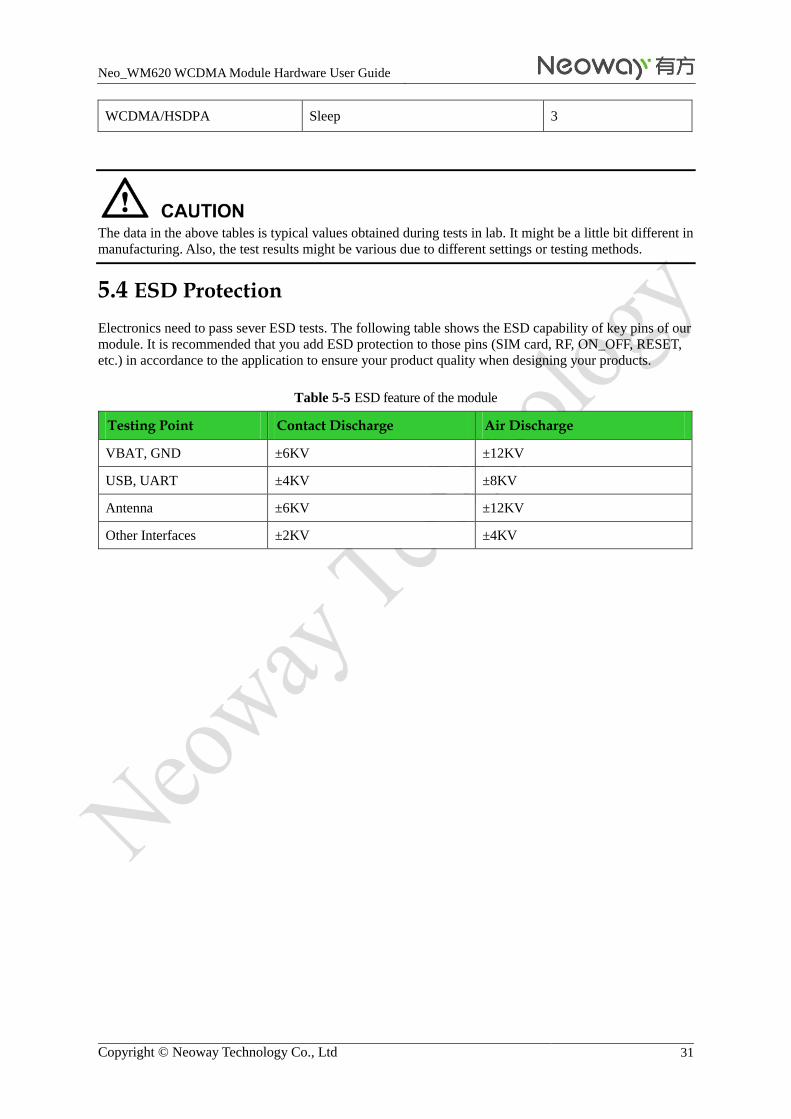
Electronics need to pass sever ESD tests. The following table shows the ESD capability of key pins of our
module. It is recommended that you add ESD protection to those pins (SIM card, RF, ON_OFF, RESET,
etc.) in accordance to the application to ensure your product quality when designing your products.
Table 5-5 ESD feature of the module
Testing Point Contact Discharge Air Discharge
VBAT, GND ±6KV ±12KV
USB, UART ±4KV ±8KV
Antenna ±6KV ±12KV
Other Interfaces ±2KV ±4KV

Neo_WM620 WCDMA Module Hardware User Guide
Copyright © Neoway Technology Co., Ltd 32
6 Typical Circuits
WM620
ON_OFF
2K
10K
VT2
MCU ON_OFF 10 nF
C3
C3 is close to the pin.
VT2
MCU RESET 10nF
C3
R6 and C3 are close to the pin.
R5
R6
R6
100
WM620
RESET
10K
2K
1
2
3
4
L5
L1
L3
L4
C14
100 pF
C13 C15
100 pF 100 pF
C16
100 pF
C18 C19
100 pF 100 pF
X26
CON-RJ11
MIC1_P
MIC1_N
EAR_P
EAR_N

Neo_WM620 WCDMA Module Hardware User Guide
Copyright © Neoway Technology Co., Ltd 33
V_MAIN
C9
1000 uF
C1
100 uF
C23
0.1 uF
C2
100 pFVBAT
R18
1K
R2
1K
D4
D2
RING
SIG_LED
UIM
_V
CC
UIM
_R
ST
UIM
_D
AT
A
UIM
_C
LK
GN
D
US
B_
D+
US
B_
D-
V_B
US
GN
D
VB
AT
1
VB
AT
2
GN
D
RE
SE
T
V_
MS
ME
_1
.8V
V_
MS
MP
_2.6
V
EA
R_
1P
EA
R_1
N
MIC
_1
N
MIC
_1P
MIC2_P
MIC2_N
GND
SPKR_P
SPKR_N
NC
NC
NC
NC
RF_ANT_F
NC
GND
GN
D
ON
_O
FF
SIG
_L
ED
HK
AIN
O
GN
D
RIN
G
CT
S
RT
S
RX
D
TX
D
NC
NC
NC
SL
EE
P
GN
D
NCNC
GND
NC
NC
NC
NC
NC
NC
NC
NC
NC
NC
GND
1
2
3
4
5
6
7
8
9
10
11
12
13
14 15
16
17
1819
20
21
22
23
24
25
26
27
28
29
30
31
32
33
34
35
36
37
38
39
40
41
42
43
4445
46
47
48
49
50
51
52
53
54
55
56
57
58
59
60
61
62
VC
ION
C17
2.0pF
C24
2.0pF
C8 100 pF
V_
UIM
_3V
UIM
_R
ST
UIM
_D
AT
A
UIM
_C
LK
US
B_D
+
US
B_
D-
VC
C5
V
RE
SE
T_IN
V_
MS
ME
_1
.8V
V_
MS
ME
_2
.6V
EA
R1
P
EA
R1N
MIC
1_
N
MIC
1_
P
V_
MA
IN
C1 1000 uF
C2 100 uF
C3 0.1 uF
C4 100 pF
MIC2_P
MIC2_N
SL
EE
P_
IN
TX
D_
1
RX
D_
1
RIN
G
SIG
_L
ED
ON
_O
FF
C25 4.7 uF
1
2
3
4
NC
SPKR_N
SPKR_P

Neo_WM620 WCDMA Module Hardware User Guide
Copyright © Neoway Technology Co., Ltd 34
7 Mounting the Module onto the
Application Board
WM620 is compatible with industrial standard reflow profile for lead-free SMT process.
The reflow profile is process dependent, so the following recommendation is just a start point guideline:
Only one flow is supported.
Quality of the solder joint depends on the solder volume. Minimum of 0.15mm stencil thickness is
recommended.
Use bigger aperture size of the stencil than actual pad size.
Use a low-residue, no-clean type solder paste.
8 Package
WM620 modules are packaged in sealed bags on delivery to guarantee a long shelf life. Package the
modules again in case of opening for any reasons.
If exposed in air for more than 48 hours at conditions not worse than 30°C/60% RH, a baking procedure
should be done before SMT. Or, if the indication card shows humidity greater than 20%, the baking
procedure is also required.
The baking should last for at least 12 hours at 90.
Neo_WM620 WCDMA Module Hardware User Guide
Copyright © Neoway Technology Co., Ltd 35
9 Abbreviations
ADC Analog-Digital Converter
AFC Automatic Frequency Control
AGC Automatic Gain Control
AMR Acknowledged multirate (speech coder)
CSD Circuit Switched Data
CPU Central Processing Unit
DAI Digital Audio interface
DAC Digital-to-Analog Converter
DCE Data Communication Equipment
DSP Digital Signal Processor
DTE Data Terminal Equipment
DTMF Dual Tone Multi-Frequency
DTR Data Terminal Ready
EFR Enhanced Full Rate
EGSM Enhanced GSM
EMC Electromagnetic Compatibility
EMI Electro Magnetic Interference
ESD Electronic Static Discharge
ETS European Telecommunication Standard
FDMA Frequency Division Multiple Access
FR Full Rate
GPRS General Packet Radio Service
GSM Global Standard for Mobile Communications
HR Half Rate
IC Integrated Circuit
IMEI International Mobile Equipment Identity
LCD Liquid Crystal Display
LED Light Emitting Diode
MS Mobile Station
PCB Printed Circuit Board
PCS Personal Communication System

Neo_WM620 WCDMA Module Hardware User Guide
Copyright © Neoway Technology Co., Ltd 36
RAM Random Access Memory
RF Radio Frequency
ROM Read-only Memory
RMS Root Mean Square
RTC Real Time Clock
SIM Subscriber Identification Module
SMS Short Message Service
SRAM Static Random Access Memory
TA Terminal adapter
TDMA Time Division Multiple Access
UART Universal asynchronous receiver-transmitter
VSWR Voltage Standing Wave Ratio
Related Documents