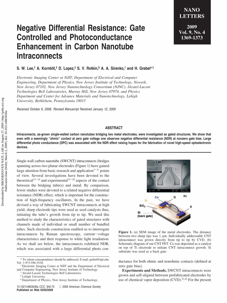
Negative Differential Resistance: Gate Controlled and Photoconductance Enhancement in Carbon Nanotube Intraconnects S. W. Lee, † A. Kornblit, ‡ D. Lopez, ‡ S. V. Rotkin, § A. A. Sirenko, | and H. Grebel* ,† Electronic Imaging Center at NJIT, Department of Electrical and Computer Engineering, Department of Physics, New Jersey Institute of Technology, Newark, New Jersey 07102, New Jersey Nanotechnology Consortium (NJNC), Alcatel-Lucent Technologies Bell Laboratories, Murray Hill, New Jersey 07974, and Physics Department and Center for AdVance Materials and Nanotechnology, Lehigh UniVersity, Bethlehem, PennsylVania 18015 Received October 6, 2008; Revised Manuscript Received January 12, 2009 ABSTRACT Intraconnects, as-grown single-walled carbon nanotubes bridging two metal electrodes, were investigated as gated structures. We show that even with a seemingly “ohmic” contact at zero gate voltage one observes negative differential resistance (NDR) at nonzero gate bias. Large differential photo conductance (DPC) was associated with the NDR effect raising hopes for the fabrication of novel high-speed optoelectronic devices. Single-wall carbon nanotube (SWCNT) intraconnects (bridges spanning across two planar electrodes (Figure 1) have gained large attention from basic research and application 1-11 points of view. Several investigations have been devoted to the theoretical 12-14 and experimental 15-20 aspects of the contact between the bridging tube(s) and metal. By comparison, fewer studies were devoted to a related negative differential resistance (NDR) effect, which is important for the construc- tion of high-frequency oscillators. In the past, we have devised a way of fabricating SWCNT intraconnects at high yield; sharp electrode tips were used as seed catalysts thus, initiating the tube’s growth from tip to tip. We used this method to study the characteristics of gated structures with channels made of individual or small number of bundled tubes. Such electrode construction enabled us to interrogate intraconnects by Raman spectroscopy, current-voltage characteristics and their response to white light irradiation. As we shall see below, the intraconnects exhibited NDR, which was associated with a large differential photo con- ductance for both ohmic and nonohmic contacts (defined at zero gate bias). Experiments and Methods. SWCNT intraconnects were grown and self-aligned between prefabricated electrodes by use of chemical vapor deposition (CVD). 21,22 For the present * To whom correspondence should be addressed. E-mail: [email protected]. Tel: 1-973-596-3538. † Electronic Imaging Center at NJIT and the Department of Electrical and Computer Engineering, New Jersey Institute of Technology. ‡ Alcatel-Lucent Technologies Bell Laboratories. § Lehigh University. | Department of Physics, New Jersey Institute of Technology. Figure 1. (a) SEM image of the metal electrodes. The distance between two sharp tips was 1 µm. Individually addressable CNT intraconnect was grown directly from tip to tip by CVD. (b) Schematic diagram of our CNT FET. Co was deposited as a catalyst on top of Ti electrode to initiate CNT intraconnect growth. Si substrate was used as a back gate. NANO LETTERS 2009 Vol. 9, No. 4 1369-1373 10.1021/nl803036a CCC: $40.75 2009 American Chemical Society Published on Web 03/02/2009 Downloaded by BROOKHAVEN NATL LAB on August 27, 2009 | http://pubs.acs.org Publication Date (Web): March 2, 2009 | doi: 10.1021/nl803036a

Welcome message from author
This document is posted to help you gain knowledge. Please leave a comment to let me know what you think about it! Share it to your friends and learn new things together.
Transcript
Negative Differential Resistance: GateControlled and PhotoconductanceEnhancement in Carbon NanotubeIntraconnectsS. W. Lee,† A. Kornblit,‡ D. Lopez,‡ S. V. Rotkin,§ A. A. Sirenko,| and H. Grebel*,†
Electronic Imaging Center at NJIT, Department of Electrical and ComputerEngineering, Department of Physics, New Jersey Institute of Technology, Newark,New Jersey 07102, New Jersey Nanotechnology Consortium (NJNC), Alcatel-LucentTechnologies Bell Laboratories, Murray Hill, New Jersey 07974, and PhysicsDepartment and Center for AdVance Materials and Nanotechnology, LehighUniVersity, Bethlehem, PennsylVania 18015
Received October 6, 2008; Revised Manuscript Received January 12, 2009
ABSTRACT
Intraconnects, as-grown single-walled carbon nanotubes bridging two metal electrodes, were investigated as gated structures. We show thateven with a seemingly “ohmic” contact at zero gate voltage one observes negative differential resistance (NDR) at nonzero gate bias. Largedifferential photo conductance (DPC) was associated with the NDR effect raising hopes for the fabrication of novel high-speed optoelectronicdevices.
Single-wall carbon nanotube (SWCNT) intraconnects (bridgesspanning across two planar electrodes (Figure 1) have gainedlarge attention from basic research and application1-11 pointsof view. Several investigations have been devoted to thetheoretical12-14 and experimental15-20 aspects of the contactbetween the bridging tube(s) and metal. By comparison,fewer studies were devoted to a related negative differentialresistance (NDR) effect, which is important for the construc-tion of high-frequency oscillators. In the past, we havedevised a way of fabricating SWCNT intraconnects at highyield; sharp electrode tips were used as seed catalysts thus,initiating the tube’s growth from tip to tip. We used thismethod to study the characteristics of gated structures withchannels made of individual or small number of bundledtubes. Such electrode construction enabled us to interrogateintraconnects by Raman spectroscopy, current-voltagecharacteristics and their response to white light irradiation.As we shall see below, the intraconnects exhibited NDR,which was associated with a large differential photo con-
ductance for both ohmic and nonohmic contacts (defined atzero gate bias).
Experiments and Methods. SWCNT intraconnects weregrown and self-aligned between prefabricated electrodes byuse of chemical vapor deposition (CVD).21,22 For the present
* To whom correspondence should be addressed. E-mail: [email protected]: 1-973-596-3538.
† Electronic Imaging Center at NJIT and the Department of Electricaland Computer Engineering, New Jersey Institute of Technology.
‡ Alcatel-Lucent Technologies Bell Laboratories.§ Lehigh University.| Department of Physics, New Jersey Institute of Technology.
Figure 1. (a) SEM image of the metal electrodes. The distancebetween two sharp tips was 1 µm. Individually addressable CNTintraconnect was grown directly from tip to tip by CVD. (b)Schematic diagram of our CNT FET. Co was deposited as a catalyston top of Ti electrode to initiate CNT intraconnect growth. Sisubstrate was used as a back gate.
NANOLETTERS
2009Vol. 9, No. 41369-1373
10.1021/nl803036a CCC: $40.75 2009 American Chemical SocietyPublished on Web 03/02/2009
Dow
nloa
ded
by B
RO
OK
HA
VE
N N
AT
L L
AB
on
Aug
ust 2
7, 2
009
| http
://pu
bs.a
cs.o
rg
Pub
licat
ion
Dat
e (W
eb):
Mar
ch 2
, 200
9 | d
oi: 1
0.10
21/n
l803
036a

study we replaced the CO precursor gas with methane/hydrogen mixture at elevated temperatures.23 While someof the intraconnects could not be observed by scanningelectron microscope (SEM), nonetheless they had a clearcurrent-voltage (I-V) and Raman scattering characteristics.The electrode construction and labeling made it easy to assessthe tubes even one year after fabrication. We made sure thatnonmetalized surfaces, away from the electrode region, didnot contribute to the electrical path. In addition, the electrodeshape enabled focusing of the laser beam, used for Ramanspectroscopy, right in-between the electrodes (see SupportingInformation). All electrical and optical measurements wereperformed at room temperature.
Figure 1 shows an SEM image of the electrodes. Here,the distance between the two electrode tips was 1 µm, thoughthe electrode layout had coaligned and laterally shiftedpatterns (Figure 1a inset). The schematic of a gated structure,made of CNT intraconnect, is shown in Figure 1b. The twometal electrodes were used as source and drain electrodes,respectively. A silicon substrate was used as a back gateelectrode. The silicon surface was oxidized to a thicknessof 20 nm prior to the electrode deposition.
Raman spectra were measured using the 514.5 nm line ofan ion Ar+ laser, a single grating spectrometer, which wasequipped with two notch filters for laser line rejection and aN2 cooled CCD detector. The system was equipped with a×50 microscope to aid focusing of the laser light betweenthe sharp tips of the electrodes. The Raman spectra of SiO2
and Si away from the bridge were used as reference andwere subtracted from the spectra of the CNT intraconnect.Broadband light illumination was made with a white-lighttungsten source, which had a high energy cutoff at 3 eV.The white-light source intensity was 0.25 mW/cm2, and itwas illuminating the entire structure.
Results. Figure 2 shows two examples, one exhibitingnonlinear and the other linear electrical characteristics. Figure2a-c shows SEM, Ids-Vds, and Raman spectra of Sample1. The nonlinear I-V curve at zero gate voltage indicates apresence of potential barrier between the tube and metalcontact(s). The asymmetry in the curve points to onedominant barrier (otherwise, the curve would have beensymmetric). Its Raman spectra are shown in Figure 2c. Thelow frequency spectra exhibit a narrow single peak (5 cm-1
wide and limited only by the system resolution) for the radialbreathing mode (RBM) at 191.9 cm-1. The peak may indicatea metallic tube (12,6) with an average diameter of 1.252nm.24 It exhibits a very large graphitic line at 1355 cm-1,which may indicate defects or, large stress. The high-frequency region exhibits two peaks at 1594 and 1567 cm-1,respectively. Their frequency difference 27 cm-1 correspondsto a tube diameter d ) 1.716 nm if we follow25 and assumea metallic type tube. It corresponds to a tube diameter d )1.329 nm assuming semiconductor type. Sample 2 exhibitslinear I-V characteristics at zero gate bias (Figure 2e). Itslow frequency Raman spectrum consists of a broader singleRBM peak (30 cm-1 wide) centered at 176.2 cm-1, whichimplies semiconductor tube(s) (11,9) with an average diam-eter of 1.365 nm. It exhibits a large defect line at 1352 cm-1.
The high-frequency frequency exhibits two peaks at 1596and 1578 cm-1, respectively. Their difference 18 cm-1
implying tube diameters d ) 2.101 nm and d ) 1.628 nmfor metallic or semiconductor type tubes, respectively.
Electrical properties in the dark and under white lightillumination were measured for Sample 1 (Figure 3) andSample 2 (Figure 4). The channel formed by the intracon-nects exhibited a natural p-type characteristics owing to thepresence of oxygen in the tubes. Figure 3a shows a map ofVgs vs Vds for the nonilluminated intraconnect. Two negativedifferential resistance (NDR) regions may be observed inthe Ids-Vgs plot: one, in the range between -3 and -6 Vand the other, around -9 V (Figure 3b-c). The NDR peakfor the first region was shifting to the negative side as theVds value increased from 0.25 to 0.75 V (Figure 3c). Thesecond NDR region was stable around -9 V. Characteristicsof the same intraconnect under illumination are shown inFigure 3d-f. Surprisingly, the light did not mask the NDReffect (Figure 3f) but locked it to the same Vgs range for all
Figure 2. Sample 1: (a) SEM image of CNT intraconnect; (b)nonlinear Ids-Vds characteristic; (c) Raman spectra with RBM at191.9 cm-1. Sample 2: (d) SEM image of CNT intraconnect; (e)linear Ids-Vds characteristic; (f) Raman spectra with RBM at 176.2cm-1.
1370 Nano Lett., Vol. 9, No. 4, 2009
Dow
nloa
ded
by B
RO
OK
HA
VE
N N
AT
L L
AB
on
Aug
ust 2
7, 2
009
| http
://pu
bs.a
cs.o
rg
Pub
licat
ion
Dat
e (W
eb):
Mar
ch 2
, 200
9 | d
oi: 1
0.10
21/n
l803
036a
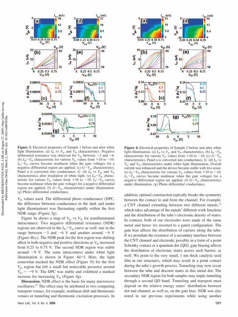
Vds values used. The differential photo conductance (DPC,the difference between conductance in the dark and underlight illumination) was fluctuating rapidly within the firstNDR range (Figure 3g).
Figure 4a shows a map of Vgs vs Vds for nonilluminatedintraconnect. Two negative differential resistance (NDR)regions are observed in the Ids-Vgs curve as well: one in therange between -3 and -6 V and another around -9 V(Figure 4b,c). The NDR peak for the first region was shiftingalbeit in both negative and positive directions as Vds increasedfrom 0.25 to 0.75 V. The second NDR region was stablearound -9 V. The same intraconnect under white lightillumination is shown in Figure 4d-f. Here, the lightsomewhat masked the NDR effect (Figure 3f) for the firstVgs region but left a small but noticeable presence aroundVgs ∼ -9 V. The DPC was stable and exhibited a markedincrease for increasing Vds (Figure 4g).
Discussion. NDR effect is the basis for many microwaveoscillators.27 The effect may be attributed to two competingtransport venues, for example, nonlinear drift and thermionicvenues or tunneling and thermionic excitation processes. In
addition, optimal construction typically breaks the symmetrybetween the contact to and from the channel. For example,a CNT channel extending between two different metals,13
which takes advantage of the metals’ different work functionsand the distribution of the tube’s electronic density of states.In contrast, both of our electrodes were made of the samemetal and hence we resorted to a gated configuration. Thegate bias affects the distribution of carriers along the tube.If we postulate the existence of a secondary interface betweenthe CNT channel and electrode, possibly in a form of a pointSchottky contact or a quantum dot (QD), gate biasing affectsthe distribution of electronic states across such barrier, aswell. We point to the very small, 1 nm thick catalytic seedfilm in our structures, which may result in a point contactduring the tube’s growth process. Tunneling may now occurbetween the tube and discrete states in this metal dot. Thesecondary NDR region for both samples may imply tunnelingthrough a second QD band. Tunneling and transport mustdepend on the relative energy states’ distribution betweendot and channel, as well as, on the gate bias. NDR was alsonoted in our previous experiments while using another
Figure 3. Electrical properties of Sample 1 before and after whitelight illumination. (a) Ids vs Vgs and Vds characteristics. Negativedifferential resistance was observed for Vgs between -2 and -6.(b) Ids-Vds characteristic for various Vgs values from +10 to -10.Ids-Vds curves become nonlinear when the gate voltages for anegative differential region are applied. (c) G-Vgs characteristics.Panel a is converted into conductance, G. (d) Ids vs Vgs and Vds
characteristics after irradiation of white light. (e) Ids-Vds charac-teristic for various Vgs values from +10 to -10. Ids-Vds curvesbecome nonlinear when the gate voltages for a negative differentialregion are applied. (f) G-Vgs characteristics under illumination.(g) Photo differential conductance.
Figure 4. Electrical properties of Sample 2 before and after whitelight illumination. (a) Ids vs Vgs and Vds characteristics. (b) Ids-Vds
characteristic for various Vgs values from +10 to -10. (c) G-Vgs
characteristics. Panel a is converted into conductance, G. (d) Ids vsVgs and Vds characteristics under white light illumination. Overallcurrent was enhanced and the device became stable with less noise.(e) Ids-Vds characteristic for various Vgs values from +10 to -10.Ids-Vds curves become nonlinear when the gate voltages for anegative differential region are applied. (f) G-Vgs characteristicsunder illumination. (g) Photo differential conductance.
Nano Lett., Vol. 9, No. 4, 2009 1371
Dow
nloa
ded
by B
RO
OK
HA
VE
N N
AT
L L
AB
on
Aug
ust 2
7, 2
009
| http
://pu
bs.a
cs.o
rg
Pub
licat
ion
Dat
e (W
eb):
Mar
ch 2
, 200
9 | d
oi: 1
0.10
21/n
l803
036a
growth technique [ref 21, Figure 3] albeit at larger gatebias.
Sample 1 is probably made of individual or of a few tubesas judged by the narrow Raman RBM spectra; its currentonly weakly dependent on gate voltage and one may attributeits behavior to mostly the Schottky point interface. Itssensitivity to the contact with electrodes led to the asymmetryin the Ids-Vds curve. In contrast, sample 2 is probably madeof a small bundle thus is more likely to portray ohmic contactat zero gate bias. Sample 2 is more responsive to the gatebias as expected of a semiconductor channel.
Raman classification of the tubes may be distorted by stressand contact to the substrate.26 In addition and despite carefulalignment (see Supporting Information), the laser spot maycover tubes, which do not contribute to electrical conductionyet, may be at resonance with the laser line thus, affectingthe Raman spectra. This could imply that both samples wereof semiconductor type if we mainly base our conclusion ona self-consistent value for the tube’s diameter. In that case,the samples differ only by the number of tubes in theirrespective bundles. Nevertheless, Raman spectroscopy is animportant characterization tool, which corroborates theexistence of nanotubes between electrodes and helps deter-mine their type, thus complementing conductance measure-ments.
The characteristics of the channel under broadband opticalexcitation corroborated these findings, as well. Opticalinduced carriers in the channel overcame the tunnelingprocess, hence the marked conductivity change for the firstNDR region (around -5 V). The optical effect is smallerfor the “nonlinear” sample 1 because of the interfering effectfrom the contact barrier. Moreover, since photoexcitedcarriers are composed of both types (holes and electrons),n-type characteristics at large positive gate voltages oughtto be exhibited. Indications to such behavior are providedin Figure 4g. Furthermore, when the graphs are plotted aslog plots (not shown) such characteristics are greatly ac-centuated. Both panels c and f of Figure 3 indicate arelatively sharp “ON” transition, which implies large channelmobility with back-to-back leaky Schottky diodes.28 The ONtransition in Figure 4c,f tends to have quadratic behavior asexpected from an ordinary semiconducting channel.
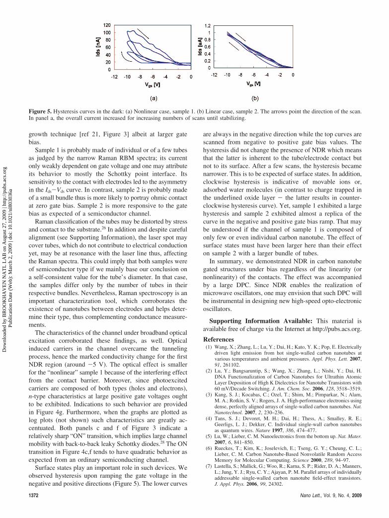
Surface states play an important role in such devices. Weobserved hysteresis upon ramping the gate voltage in thenegative and positive directions (Figure 5). The lower curves
are always in the negative direction while the top curves arescanned from negative to positive gate bias values. Thehysteresis did not change the presence of NDR which meansthat the latter is inherent to the tube/electrode contact butnot to its surface. After a few scans, the hysteresis becamenarrower. This is to be expected of surface states. In addition,clockwise hysteresis is indicative of movable ions or,adsorbed water molecules (in contrast to charge trapped inthe underlined oxide layer - the latter results in counter-clockwise hysteresis curve). Yet, sample 1 exhibited a largehysteresis and sample 2 exhibited almost a replica of thecurve in the negative and positive gate bias ramp. That maybe understood if the channel of sample 1 is composed ofonly few or even individual carbon nanotube. The effect ofsurface states must have been larger here than their effecton sample 2 with a larger bundle of tubes.
In summary, we demonstrated NDR in carbon nanotubegated structures under bias regardless of the linearity (ornonlinearity) of the contacts. The effect was accompaniedby a large DPC. Since NDR enables the realization ofmicrowave oscillators, one may envision that such DPC willbe instrumental in designing new high-speed opto-electronicoscillators.
Supporting Information Available: This material isavailable free of charge via the Internet at http://pubs.acs.org.
References(1) Wang, X.; Zhang, L.; Lu, Y.; Dai, H.; Kato, Y. K.; Pop, E. Electrically
driven light emission from hot single-walled carbon nanotubes atvarious temperatures and ambient pressures. Appl. Phys. Lett. 2007,91, 261102.
(2) Lu, Y.; Bangsaruntip, S.; Wang, X.; Zhang, L.; Nishi, Y.; Dai, H.DNA Functionalization of Carbon Nanotubes for Ultrathin AtomicLayer Deposition of High K Dielectrics for Nanotube Transistors with60 mV/Decade Switching. J. Am. Chem. Soc. 2006, 128, 3518–3519.
(3) Kang, S. J.; Kocabas, C.; Ozel, T.; Shim, M.; Pimparkar, N.; Alam,M. A.; Rotkin, S. V.; Rogers, J. A. High-performance electronics usingdense, perfectly aligned arrays of single-walled carbon nanotubes. Nat.Nanotechnol. 2007, 2, 230–236.
(4) Tans, S. J.; Devoret, M. H.; Dai, H.; Thess, A.; Smalley, R. E.;Geerligs, L. J.; Dekker, C. Individual single-wall carbon nanotubesas quantum wires. Nature 1997, 386, 474–477.
(5) Lu, W.; Lieber, C. M. Nanoelectronics from the bottom up. Nat. Mater.2007, 6, 841–850.
(6) Rueckes, T.; Kim, K.; Joselevich, E.; Tseng, G. Y.; Cheung, C. L.;Lieber, C. M. Carbon Nanotube-Based Nonvolatile Random AccessMemory for Molecular Computing. Science 2000, 289, 94–97.
(7) Lastella, S.; Mallick, G.; Woo, R.; Karna, S. P.; Rider, D. A.; Manners,L.; Jung, Y. J.; Ryu, C. Y.; Ajayan, P. M. Parallel arrays of individuallyaddressable single-walled carbon nanotube field-effect transistors.J. Appl. Phys. 2006, 99, 24302.
Figure 5. Hysteresis curves in the dark: (a) Nonlinear case, sample 1. (b) Linear case, sample 2. The arrows point the direction of the scan.In panel a, the overall current increased for increasing numbers of scans until stabilizing.
1372 Nano Lett., Vol. 9, No. 4, 2009
Dow
nloa
ded
by B
RO
OK
HA
VE
N N
AT
L L
AB
on
Aug
ust 2
7, 2
009
| http
://pu
bs.a
cs.o
rg
Pub
licat
ion
Dat
e (W
eb):
Mar
ch 2
, 200
9 | d
oi: 1
0.10
21/n
l803
036a

(8) Kish, L. B.; Ajayan, P. M. Terrabyte flash memory with carbonnanotubes. Appl. Phys. Lett. 2005, 86, 93106.
(9) Bosnick, K.; Gabor, N.; McEuen, P. L. Transport in carbon nanotubep-i-n diodes. Appl. Phys. Lett. 2006, 89, 163121.
(10) Rosenblatt, S.; Yaish, Y; Park, J.; Gore, J.; Sazonova, V.; McEuen,P. L. High performance electrolyte gated carbon nanotube transistors.Nano Lett. 2002, 2, 869.
(11) Chen, Z.; Appenzeller, J.; Lin, Y.-M.; Sippel-Oakley, J.; Rinzler, A. G.;Tang, J.; Wind, S. J.; Solomon, P. M.; Avouris, P. An Integrated LogicCircuit Assembled on a Single Carbon Nanotube. Science 2006, 311,1735.
(12) Leonard, F.; Tersoff, J. Multiple Functionality in Nanotube Transistors.Phys. ReV. Lett. 2002, 88, 258302.
(13) Leonard, F.; Tersoff, J. Negative Differential Resistance in NanotubeDevices. Phys. ReV. Lett. 2000, 85, 4767.
(14) Farajian, A. A.; Esfarjani, K.; Kawazoe, Y. Nonlinear CoherentTransport Through Doped Nanotube Junctions. Phys. ReV. Lett. 1999,92, 5084.
(15) Zhou, C.; Kong, J.; Yenilmez, E.; Dai, H. Modulated Chemical Dopingof Individual Carbon Nanotubes. Science 2000, 290, 1552.
(16) Yuzvinsky, T. D.; Mickelson, W.; Aloni, S.; Begtrup, G. E.; Kis, A.;Zettl, A. Shrinking a Carbon Nanotube. Nano Lett 2006, 6, 2718–2722.
(17) Iliea, A.; Egger, S.; Friedrichs, S.; Kang, D.-J.; Green, M. L. H.Correlated transport and high resolution transmission electron mi-croscopy investigations on inorganic-filled single-walled carbon nano-tubes showing negative differential resistance. App. Phys. Lett. 2007,91, 253124.
(18) Li, X-F.; Chen, K.-Q.; Wang, L.; Long, M.-Q.; Zou, B. S.; Shuai, Z.Effect of length and size of heterojunction on the transport propertiesof carbon-nanotube devices. App. Phys. Lett. 2007, 91, 133511.
(19) Javey, A.; Guo, J.; Wang, Q.; Lundstrom, M.; Dai, H. Ballistic carbonnanotube field-effect transistors. Nature 2003, 424, 654.
(20) Heinze, S.; Tersoff, J.; Martel, R.; Derycke, V.; Appenzeller, J.;Avouris, P. Carbon Nanotubes as Schottky Barrier Transistors. Phys.ReV. Lett. 2002, 89, 106801.
(21) Katz, D.; Lopez, D.; Kornblit, A.; Grebel, H. Electrical and OpticalProperties of Individual Carbon Nanotubes Bridging Addressable MetalElectrode Tips. J. Nanosci. Nanotechnol. 2008, 8, 1–5.
(22) Katz, D.; Lee, S.-W.; Lopez, D.; Kornblit, A.; Grebel, H. Synthesisof Carbon Nanotubes: Controlled Interconnects Growth. J. Vac. Sci.and Tech., B 2007, B25, 1191.
(23) Kong, J.; Soh, H. T.; Cassell, A.; Quate, C. F.; Dai, H. Synthesis ofIndividual Single-Walled Carbon Nanotubes on Patterned SiliconWafers. Nature 1998, 395, 878.
(24) Krupke, R.; Hennrich, F.; Lohneysen, H. V.; Kappes, M. M. Separationof Metallic from Semiconducting Single-walled Carbon Nanotubes.Science 2003, 301, 344–347.
(25) Jorio, A.; Filho, A. G. S.; Dresselhaus, G.; Dresselhaus, M. S.; Swan,A. K.; Unlu, M. S.; Goldberg, B. B.; Pimenta, M. A.; Hafner, J. H.;Lieber, C. M.; Saito, R. G-band resonant Raman study of 62 isolatedsingle-wall carbon nanotubes. Phys. ReV B 2002, 65, 155412.
(26) Zhang, Y.; Son, H.; Zhang, J.; Dresselhaus, M. S.; Kong, J.; Liu, Z.Raman Spectra Variation of Partially Suspended Individual Single-Walled Carbon Nanotubes. J. Phys. Chem. C. 2007, 111, 1983–1987.
(27) Sze, S. M. Physics of Semiconductor DeVices; Wiley-Interscience, NewYork, 1981.
(28) Lee, S. W., Grebel, H.; Kornblit, A.; Lopez, D. Electrical and opticalproperties of carbon nanotube/polypyrrole addressable intra-connects.Synth. Met. [Online early access]. DOI: 10.1016/j.synthmet.2008.11.015.Published online: January 11, 2009.
NL803036A
Nano Lett., Vol. 9, No. 4, 2009 1373
Dow
nloa
ded
by B
RO
OK
HA
VE
N N
AT
L L
AB
on
Aug
ust 2
7, 2
009
| http
://pu
bs.a
cs.o
rg
Pub
licat
ion
Dat
e (W
eb):
Mar
ch 2
, 200
9 | d
oi: 1
0.10
21/n
l803
036a
Related Documents