ISSN 1541-308X, Physics of Wave Phenomena, 2009, Vol. 17, No. 2, pp. 77–91. c Allerton Press, Inc., 2009. LASER SPECTROSCOPY Nd 3+ :GGG and Cr 4+ :GGG Epitaxial Films for Neodymium Lasers G. A. Bufetova 1* , M. Yu. Gusev 2 , I. A. Ivanov 2 , N. S. Neustroev 2 , D. A. Nikolaev 1 , V. F. Seregin 1 , V. B. Tsvetkov 1 , and I. A. Shcherbakov 1 1 Research Center for Laser Materials and Technologies, Prokhorov General Physics Institute, Russian Academy of Sciences, ul. Vavilova 38, Moscow, 119991 Russia 2 Research Institute of Materials Science and Technology, Zelenograd, Moscow, 124460 Russia Received November 18, 2008 Abstract—An efficient technology was developed for growing the gadolinium gallium garnet (GGG) single-crystal films doped with Nd 3+ or Cr and Ca ions. The films with thickness up to 100 μm have been grown by liquid-phase epitaxy method on undoped GGG substrates of small and big sizes (5−8 mm and up to 76 mm in diameter, respectively). The dependence of absorption, luminescence spectra and optical losses at the wavelength of 1 μm on growth temperature and melt-solution composition was studied. We demonstrated that Cr 4+ centers have been implemented in epitaxial films and these films may be used as passive Q-switches for laser systems. PACS numbers : 42.55.Px, 42.60.Gd, 42.70.Hj, 81.15.Lm DOI: 10.3103/S1541308X09020010 1. INTRODUCTION Great progress has been made in the development of high-efficiency solid-state diode-pumped lasers during the last 20 years [1−6]. Commercial lasers of this type are widely used, for example, in laser rangefinders and lidars [7], labeling tools [8], and medicine [9]. This is due to a great extent to the progress in diode pump systems operating in a wide power range (from 10 −3 to 10 4 W). At the same time, the use of active elements of conventional shape meets serious difficulties, related to the formation of a pump beam of necessary geometry (strongly divergent pump radiation must be transformed into a long narrow beam). As a result, such systems become not only more complicated and expensive but also less efficient in many cases. Lasers and amplifiers with optical (diode) pumping are most effective when the waveguide geometry is used, in which pump radiation is strongly overlapped with cavity modes, the volume of laser modes is min- imized, and the product of the pump intensity with the interaction length may exceed the corresponding values for the bulk active elements by several orders of magnitude. This concept is implemented in erbium fiber amplifiers, ytterbium fiber lasers, etc. Currently, * E-mail: [email protected] the average lasing power of a fiber laser with a core di- ameter of about 8 μm reaches 1.5 kW, and the lasing pulse energy is limited by several microjoules. The lasing power in planar elements is limited by several hundreds of watts, and the lasing energies in the Q- switched mode are at a level of 0.5 J. Another ad- vantage of planar active elements over classical ones is smaller thermo-optical beam distortions [10, 11]. Therefore, the researchers all over the world pay much attention to the methods for fabricating both fiber and planar active elements. The studies devoted to design of planar optical waveguides based on garnet crystals doped with rare earth ions have been under way since the 1970s [12, 13]. However, the films obtained by different methods in the first studies were of low crystalline and optical quality, and it was fairly difficult to obtain lasing even on neodymium active elements [14]. Moreover, the luminescence spectra of neodymium ions differed from those of Czochralski-grown bulk single crystals. The methods of ion implantation [15, 16] and thermal diffusion [16], which have been thoroughly elaborated in electronic technology and production of electronic devices, make it possible to easily obtain waveguide structures in glasses and crystals of different types, including nonlinear. The thus 77

Welcome message from author
This document is posted to help you gain knowledge. Please leave a comment to let me know what you think about it! Share it to your friends and learn new things together.
Transcript
ISSN 1541-308X, Physics of Wave Phenomena, 2009, Vol. 17, No. 2, pp. 77–91. c© Allerton Press, Inc., 2009.
LASER SPECTROSCOPY
Nd3+:GGG and Cr4+:GGG Epitaxial Filmsfor Neodymium Lasers
G. A. Bufetova1*, M. Yu. Gusev2, I. A. Ivanov2, N. S. Neustroev2,D. A. Nikolaev1, V. F. Seregin1, V. B. Tsvetkov1, and I. A. Shcherbakov1
1Research Center for Laser Materials and Technologies, Prokhorov General Physics Institute,Russian Academy of Sciences, ul. Vavilova 38, Moscow, 119991 Russia
2Research Institute of Materials Science and Technology, Zelenograd, Moscow, 124460 Russia
Received November 18, 2008
Abstract—An efficient technology was developed for growing the gadolinium gallium garnet (GGG)single-crystal films doped with Nd3+ or Cr and Ca ions. The films with thickness up to 100 μm have beengrown by liquid-phase epitaxy method on undoped GGG substrates of small and big sizes (5−8 mm andup to 76 mm in diameter, respectively). The dependence of absorption, luminescence spectra and opticallosses at the wavelength of 1 μm on growth temperature and melt-solution composition was studied. Wedemonstrated that Cr4+ centers have been implemented in epitaxial films and these films may be used aspassive Q-switches for laser systems.
PACS numbers : 42.55.Px, 42.60.Gd, 42.70.Hj, 81.15.LmDOI: 10.3103/S1541308X09020010
1. INTRODUCTION
Great progress has been made in the developmentof high-efficiency solid-state diode-pumped lasersduring the last 20 years [1−6]. Commercial lasersof this type are widely used, for example, in laserrangefinders and lidars [7], labeling tools [8], andmedicine [9]. This is due to a great extent to theprogress in diode pump systems operating in a widepower range (from 10−3 to 104 W). At the sametime, the use of active elements of conventional shapemeets serious difficulties, related to the formationof a pump beam of necessary geometry (stronglydivergent pump radiation must be transformed into along narrow beam). As a result, such systems becomenot only more complicated and expensive but also lessefficient in many cases.
Lasers and amplifiers with optical (diode) pumpingare most effective when the waveguide geometry isused, in which pump radiation is strongly overlappedwith cavity modes, the volume of laser modes is min-imized, and the product of the pump intensity withthe interaction length may exceed the correspondingvalues for the bulk active elements by several ordersof magnitude. This concept is implemented in erbiumfiber amplifiers, ytterbium fiber lasers, etc. Currently,
*E-mail: [email protected]
the average lasing power of a fiber laser with a core di-ameter of about 8 μm reaches 1.5 kW, and the lasingpulse energy is limited by several microjoules. Thelasing power in planar elements is limited by severalhundreds of watts, and the lasing energies in the Q-switched mode are at a level of 0.5 J. Another ad-vantage of planar active elements over classical onesis smaller thermo-optical beam distortions [10, 11].Therefore, the researchers all over the world pay muchattention to the methods for fabricating both fiber andplanar active elements.
The studies devoted to design of planar opticalwaveguides based on garnet crystals doped with rareearth ions have been under way since the 1970s[12, 13]. However, the films obtained by differentmethods in the first studies were of low crystallineand optical quality, and it was fairly difficult to obtainlasing even on neodymium active elements [14].Moreover, the luminescence spectra of neodymiumions differed from those of Czochralski-grown bulksingle crystals.
The methods of ion implantation [15, 16] andthermal diffusion [16], which have been thoroughlyelaborated in electronic technology and productionof electronic devices, make it possible to easilyobtain waveguide structures in glasses and crystalsof different types, including nonlinear. The thus
77

78 BUFETOVA et al.
obtained structures have high optical character-istics but relatively large loss at a wavelength of1 μm (∼1 dB cm−1). The neodymium- and erbium-activated structures, obtained by the above-men-tioned methods, exhibited lasing at wavelengths of1 and 3 μm. In particular, in a 20-μm Nd:YAG planarwaveguide prepared by ion implantation, the lasingthreshold was ∼1 mW at 808-nm laser-diode pump-ing. The lasing efficiency was ∼15%. The poor lasercharacteristics were explained by both the low pumpefficiency and high loss at the lasing wavelength. Theloss source was not exactly determined. However, themost likely reason was the damage of the substratecrystalline structure, induced by an ion beam.
The method for obtaining planar structures bylaser sputtering with subsequent deposition on a sub-strate [14, 17] may be optimal for preparing multi-component thin films due to the possibility of con-gruent target-to-substrate transport of material. Inaddition, this technique does not require to matchthe film and substrate lattice parameters. Moreover,single-crystal films can be deposited even on glasssubstrates [21]. The loss at a lasing wavelengthof 1 μm in the structures fabricated in this way isalso high (2−6 dB cm−1). Nevertheless, lasing wasobtained on neodymium planar structures producedby this method. However, the lasing efficiency did notexceed 20% of the absorbed pump power.
The methods of vapor-phase epitaxy (VPE) [18]and liquid-phase epitaxy (LPE) [19, 20] are morecomplex in comparison with those considered above,because growth of high-quality films requires carefulmatching of the substrate and film lattice parametersand choice of appropriate thermal growth conditions.However, specifically these methods make it possibleto obtain planar structures of the highest quality withthe least loss at the lasing wavelength. For example,samples of Yb:YAG planar structures with a lossless than 0.05 dB cm−1 (i.e., about 0.12 cm−1) at awavelength of 1 μm have been implemented. Thisvalue exceeds the loss in commercial crystals grownby the Czochralski method by a factor of only two.In this case, the lasing efficiency under laser-diodepumping was about 77% of the diode power [22]. Adrawback of VPE is the low growth rate and smallfilm thickness.
The interest in garnet crystals activated with Cr4+
ions is caused by their wide practical application inQ-switches for 1-μm lasers and in tunable near-IR(1.2−1.5 μm) lasers. The growth technique of bulkCr4+:YAG and Cr4+:GGG crystals has been devel-oped for more than 15 years [23]. Currently, thestudies aimed at improving the optical characteristicsof Cr-containing garnets and developing a physicalmodel to explain the mechanism of formation of Cr4+
ions in crystals are under way [24−26]. Compactlaser systems are of particular interest: they mustbe based on effective (simple, reliable, and inexpen-sive) short-pulse lasers with stable single-mode las-ing [27]. A possible design is a single block composedof a crystalline active element and an epitaxial single-crystal layer on its surface, operating as a Q-switch[28, 29]. This is a complex technological problem tobe solved in several stages.
The purpose of this study was to search for the op-timal conditions for obtaining high-quality homoge-neous single-crystal gadolinium gallium garnet films,doped with neodymium and chromium ions, on sub-strates of large diameter (more than 70 mm), anddetermine the spectroscopic characteristics for theiruse as active elements and Q-switches in compactlaser systems.
2. DEVELOPMENT OF THE METHODSFOR GROWING SINGLE-CRYSTALEPITAXIAL FILMS WITH GARNETSTRUCTURE AND OPTIMIZATION
OF GROWTH CONDITIONS
An analysis of the data in the literature showsthat VPE and LPE make it possible to obtain planarstructures of the highest quality and least loss at alasing wavelength. However, VPE barely makes itpossible to grow films up to 100 μm thick. Therefore,we chose LPE to grow laser garnet films for planaractive elements. Growth of epitaxial films from melt-solution allows one to vary the growth temperature ina certain range in order to optimize the film param-eters. We used immersion in a supersaturated melt-solution with garnet components.
As a substrate and film material, we chose crystalswith garnet structure (in particular, gadolinium gal-lium garnet (GGG)) for the following reasons:
(i) modern technology makes it possible to growcrystals up to 150 mm in diameter, due to which notonly optical elements with a large aperture can beprepared but also elements of smaller sizes with moreuniform properties;
(ii) chemical (thermodynamic) stability and me-chanical strength of these crystals facilitate their use;
(iii) high thermal conductivity allows high-powerapplications;
(iv) the presence of ions of different size in thegarnet composition facilitates doping with differentelements.
In this study, the emphasis was on the growthof two epitaxial films of different composition, dopedwith Nd3+ ions or Ca2+, Cr3+, and Cr4+ ions, withminimization of optical loss at a wavelength of 1 μm.
PHYSICS OF WAVE PHENOMENA Vol. 17 No. 2 2009

Nd3+:GGG AND Cr4+:GGG EPITAXIAL FILMS 79
The melt-solution composition, dopant concen-tration, and growth conditions differed upon dopingwith Nd3+ ions or with Ca2+, Cr3+, and Cr4+ ions.However, there are general regularities of doped filmgrowth on undoped substrates, including the meth-ods for eliminating lattice parameter mismatch.
The melt contains the corresponding garnet-forming oxides of rare earth elements (RE2O3), en-tering the dodecahedral sublattice, and oxides of met-als (M2O3) entering the octahedral and tetrahedralgarnet crystal sublattices, along with a mixture of lead(PbO) and boron (B2O3) oxides. The garnet domainin the phase diagram of the PbO−M2O3−RE2O3
pseudoternary system is fairly limited. To providegarnet growth, the M2O3 content in the melt-solution should exceed the stoichiometric (for garnet)value. At lower M2O3 contents, a nongarnet phase issynthesized. Initially, the mixture of starting oxides ismolten at a temperature of about 1200◦C for 6 h. Togrow a film, the melt-solution temperature (tg) shouldbe maintained below the liquidus temperature tL andthe saturation temperature ts. Thus, the growthtemperature tg = tL − Δt, where Δt = 0.5−150◦C.
First, substrates are slowly heated to the growthtemperature in the heating zone to exclude PbOdeposition on the cold substrates. Then the sub-strates are immersed in the melt-solution located inthe growth zone. Simultaneously, the substrates arerotated with the rate ω = 30−200 rpm. The growthrate is very sensitive to the substrate rotation rate andsupercooling; it is generally proportional to Δt and ω.When the grown layer reaches the specified thicknessh, the substrates are extracted from the melt andbrought into rotation at a high (ω � 800 rpm) rateto remove the residual melt from the film or holder,with subsequent slow lift (for more than 2 min) toprevent a heat shock and cracking upon rapid cooling.The entire set is washed in warm diluted nitric acidand deionized water, after which the substrates areremoved from the holder.
The critical LPE factors are the composition andtemperature of the melt and the constancy of tem-perature and rotation rate. When growing films, itis necessary to take special measures to provide ahigh degree of purity of the substrates and holder andexclude the presence of particular contaminations.It is also necessary to use sufficiently long expo-sures upon heating and cooling to ensure thermalequilibrium and prevent a heat shock. If these fac-tors are not properly controlled, the film compositionand/or thickness may differ from the specified values.In addition, even when all necessary conditions areprovided, defects caused by nonuniform growth orfaceting may arise in the film.
Thus, we can select four main factors in epitaxialfilm growth, which must be carefully controlled:
(i) phase equilibrium in the continuously chang-ing garnet melt-solution composition;
(ii) epitaxial crystallization from a supercooledmelt;
(iii) depletion and feeding of the boundary layer;(iv) distribution of elements in the melt−film
system.The melt-solution composition changes during
crystallization. Naturally, crystallization occurs atthe crystal/melt-solution interface; thus, depletionof the garnet components is observed in this regionduring growth, which is compensated for by feedingfrom the melt-solution. The physical processesresponsible for feeding lead to a continuous change inthe concentration in the boundary layer of thicknessδ; i.e., C = C(x, t) in this layer. The concentrationCg at the interface is determined by the relative ratesof crystallization and transport of melt-solution com-ponents to the crystallization front. Crystallizationdepends on the concentration Cg and temperature.Thus, the crystallization rate is limited by diffusionand convection in the melt-solution; this fact leads (inthe first-order approximation) to a linear dependenceof the film growth rate on the supercooling Δt (Fig. 1)and a square-root dependence on the rotation rate,ω1/2 (Fig. 2).
Along with the effect of process parameters on thegrowth rate, it is also necessary to take into accounttheir effect on the film composition. The ratio of dif-ferent components in the melt-solution significantlydiffers from that in the film grown. To determinethe boundaries of the primary (garnet) phase field,melt-solution characteristics, and some properties of
Fig. 1. Temperature dependences of the growth rate forgarnet melts with different concentrations CL (g cm−3)and liquidus temperatures tL (◦C).
PHYSICS OF WAVE PHENOMENA Vol. 17 No. 2 2009

80 BUFETOVA et al.
Table 1. Compositions and main characteristics of the melt-solutions used to optimize the growth technique of Nd-activated films
No. Molar fractions R1 R3 R4 ts, ◦C
PbO B2O3 Gd2O3 Ga2O3 Nd2O3
1 87.400 7.400 1.2000 4.0000 — 3.33 11.8 0.052 9702 84.100 7.070 0.5000 8.3300 — 16.67 11.8 0.0833 9703 87.300 7.350 0.3150 5.2500 — 25 11.8 0.05565 8624 83.200 7.050 0.3750 9.3750 — 25 11.8 0.0975 9415 92.950 2.000 0.4589 4.5890 — 10 46.5 0.0505 10426 91.500 2.000 0.2500 6.2600 — 25 46 0.065 9907 97.360 0 2.4000 0.2400 — 10 — 0.0268 10028 98.240 0 1.6000 0.1600 — 10 — 0.0176 9009 92.085 3.070 0.4600 4.3850 — 9.5 30 0.04845 900
10 87.210 5.814 0.4360 6.5395 — 15 15 0.0698 98211 87.206 5.814 0.4359 6.5410 0.0036 15 15 0.0699 98212 87.203 5.813 0.4359 6.5406 0.0072 15 15 0.06995 98213 87.200 5.813 0.4359 6.5404 0.0108 15 15 0.0700 970
crystallizing garnets, molar ratios were introducedinto practice [30]. We use only the following ratios:
M2O3∑RE2O3
≡ R1,
M2O3
M2O3+MO2≡ R2,
PbOB2O3
≡ R3,
∑RE2O3+M2O3+MO2
PbO+B2O3+∑
RE2O3+M2O3+MO2≡ R4,
MOMO+MO2
≡ R5,MO
∑RE2O3
≡ R6,
Fig. 2. Dependences of the growth rate on the substraterotation rate for compositions 1 and 2 (see notation inFig. 1).
where ΣRE2O3 is the sum of molar concentrations ofrare earth oxides; M2O3 and MO2 are the molar con-centrations of oxides of tri- and tetravalent metals,entering the octahedral and tetrahedral sublattices;and MO is the molar concentration of the oxide of thedivalent metal, which enters the rare earth sublattice(dodecahedron).
The relative amounts of the elements forming agarnet film depend on their contents in the melt-solution and the growth conditions. Therefore, therelation between the melt-solution and film compo-sitions is a complex function.
3. GROWTH OF SINGLE-CRYSTALEPITAXIAL FILMS
DOPED WITH Nd3+ IONSAND OPTIMIZATION
OF GROWTH CONDITIONS
The melt-solution composition and growth condi-tions that are most appropriate for growth of GGGepitaxial structures doped with Nd3+ ions weresought for within the system formed by PbO−B2O3
(solvent) and Gd2O3− Ga2O3 (garnet-forming com-ponents). The melt-solution compositions used in theoptimization stage and their characteristics are listedin Table 1.
Epitaxial films were doped with Nd3+ ions bymeans of additional introduction of Nd2O3 oxide intothe most efficient melt-solution No. 10 (compositions11−13).
Gd3Ga5O12 (GGG) and NdxGd3−xGa5O12
(Nd:GGG) films were grown on 76-mm GGG sub-strates. To determine the kinetic features of the
PHYSICS OF WAVE PHENOMENA Vol. 17 No. 2 2009

Nd3+:GGG AND Cr4+:GGG EPITAXIAL FILMS 81
Table 2. Characteristics of the samples of garnet epitaxialstructures obtained in the optimization stage
Sample∗ Sample size Δt, h, Nd3+ ionsdiameters, ◦C μm concentration∗∗,
mm cm−3
7-1 76 53 25 —
7-2 76 12 15 —
10-3 76 62 20 —
10-4 76 8 11.6 —
11-5 76 8 13.6 1×10²⁰
12-6 76 8 13.2 2×10²⁰
13-7 76 8 12.8 3×10²⁰
N o t e s: ∗ the first number indicates the melt-solution compo-sition from Table 1 and the second is the sample serial number;∗∗ calculated value.
solutions, along with the film growth at tg < ts, weperformed experiments at temperatures exceeding thesaturation temperature ts. In this case, dissolution(melting) of substrate was observed (the so-callednegative growth). The thicknesses of the film anddissolved (etched) substrate layer were determined byweighing the wafers before and after the process, withfurther calculation taking into account the single-crystal GGG density (7.068 g cm−3). Under thesealing zone conditions and with provided necessarysample purity, the data obtained correlated well withthe method for determining the film thickness froma cleavage: ±1−3% (for thicknesses of 2 μm andmore). Since cleavage preparation leads to sampledestruction, this method cannot be used for 100%monitoring.
Table 2 contains the data on the series of sam-ples grown from melt-solution for further study[7, 10−13]. The substrates were wafers cut fromthe same GGG crystal (orientation (111) ±2′′) andhaving the same (up to the fifth decimal place whichis measurement error in our case) substrate latticeparameter: as = 12.38254 A.
The results obtained suggest that melt-solutionsNos. 1, 2, 6, 7, and 10 are most appropriate forgrowing epitaxial Nd3+-doped GGG films on GGGsubstrates. These melt-solutions are characterizedby the most effective parameters: moderate slope ofthe temperature dependence of the growth rate, opti-mal saturation temperature (950 � ts < 1000◦C), andlow solvent (PbO) evaporation. It was experimentallyfound that addition of Nd2O3 to melt-solution No. 10in amounts necessary for obtaining Nd3+ concentra-tions of 1×10²⁰, 2×10²⁰, and 3×1020 cm−3 in the
films barely affects the liquidus temperature of the so-lution. This circumstance is favorable for the processpurity.
To determine the effect of melt-solution composi-tion on the film−substrate lattice mismatch, we per-formed a series of experiments on Nd3Ga5O12 garnetepitaxial growth on a Gd3Ga5O12 substrate. Themain purpose was to analyze the effect of variation inthe garnet-forming ion ratios in the solution.
First charge composition (Nd 1):0.872 mol%Nd2O3−8.968 mol%Ga2O3−86.95 mol%PbO−3.48 mol%B2O3,
[Ga2O3][Nd2O3]
= 10.
In these experiments, we obtained samples with afaceted surface (Fig. 3(a)). X-ray diffraction analysisshowed stress relaxation; i.e., the measured film lat-tice parameter a⊥f = 12.516 A only slightly differs fromthe equilibrium value a⊥f = 12.509 A for Nd3Ga5O12.
An important difference between the films ob-tained and those investigated previously (undoped
Fig. 3. Surface morphology of the Nd3Ga5O12/Gd3Ga5O12 films grown under optimal conditions:(a) melt Nd 1, tg = 840◦C and (b) melt Nd 2, tg = 837◦C
PHYSICS OF WAVE PHENOMENA Vol. 17 No. 2 2009
82 BUFETOVA et al.
garnets) is the presence of coarser surface structures(with a larger period of surface irregularities). Thedifferences in the growth conditions are as follows:
(i) another chemical composition of the epitaxialfilm;
(ii) large lattice mismatch (at the growthtemperature):
Δa
a
(Nd3Ga5O12
GGG
)
= 1.01%,
Δa
a
(Gd3Ga5O12
GGG
)
= 0.06%;
(iii) higher (by a factor of 2−3) relative and ab-solute concentrations of the rare earth componentRE2O3 in the melt-solution.
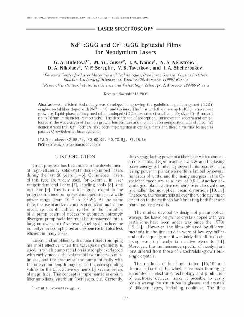
At a higher epitaxial growth temperature, a sam-ple with isolated islands was obtained. All nucleihad pronounced faceting and clearly observed first-and second-order faces, {110} and {211}, respectively(Fig. 4).
Second charge composition (Nd 2):
0.462 mol%Nd2O3−27.81 mol%Ga2O3−69.5 mol%PbO−2.22 mol%B2O3,
[Ga2O3][Nd2O3]
= 60.
The main difference from the previous melt is alower Nd2O3 concentration.
As a result, as in the previous experiments, weobtained samples reflecting different crystallizationconditions: from isolated faceted nuclei to a contin-uous faceted film (Fig. 3(b)).
The main result was a shallower texture. Thefilm lattice parameter was close to the equilibriumvalue for a single crystal of the same composition (asituation typical of faceted films).
The experiments on growth of homogeneous(in composition and lattice parameter) films witha film−substrate lattice mismatch showed someregularities common for different compositions.
(i) The temperature dependence of the growth ratehas a characteristic step at t = tcr (film grows att � tcr, while at t > tcr the growth is absent). In thiscase, the step height depends on the lattice mis-match (the larger the mismatch Δa =af − as, thelarger δt = ts − tcr).
(ii) The inclined portion of the temperature de-pendence of the growth rate is independent of thefilm strain; i.e., the points corresponding to faceted(with relaxed mismath), single-crystal strained, andsingle-crystal unstrained films lie in a straight line,
Fig. 4. Crystallization of Nd3Ga5O12/ Gd3Ga5O12:(a) isolated and (b) outgrown nuclei.
which characterizes the temperature dependence ofthe growth rate.
(iii) At the critical temperature (corresponding tothe kink in the dependence V (T )), individual nucleigrow instead of a continuous film; in this case, thefaceting of nuclei corresponds to the garnet habit.Growth is absent at temperatures above critical.
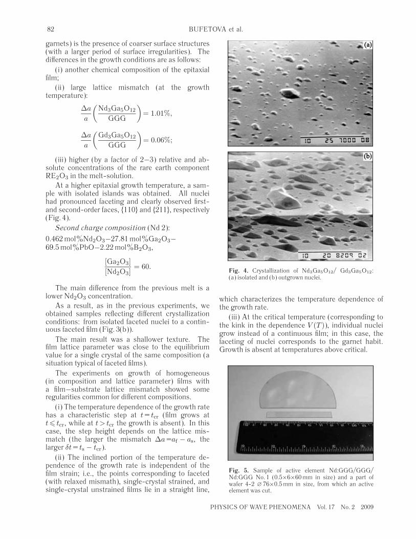
Fig. 5. Sample of active element Nd:GGG/GGG/Nd:GGG No. 1 (0.5×6×60 mm in size) and a part ofwafer 4-2 ∅ 76×0.5 mm in size, from which an activeelement was cut.
PHYSICS OF WAVE PHENOMENA Vol. 17 No. 2 2009

Nd3+:GGG AND Cr4+:GGG EPITAXIAL FILMS 83
Table 3. Characteristics of garnet epitaxial structures activated with Nd ions
Sample Sample size, Substrate Film Concentrationmm orientation thickness, of Nd3+ ions, cm−3
μm (calculation)
1-1 ∅ 30×0.3 (111)± 20′ 5.0 1×10²³
2-1 ∅ 30×0.5 (100)± 20′ 8.0 1×10²³
5-2 ∅ 76×0.3 (100)± 20′ 5.0 6×10²⁰
3-1 ∅ 76×0.5 (111)± 20′ 25.0 1.5×10²⁰
4-1 ∅ 76×0.46 (111)± 20′ 14.8 3×10²⁰
4-2 ∅ 76×0.54 (111)± 20′ 50.0 2×10²⁰
5-3 ∅ 76×0.51 (100)± 20′ 20.0 6×10²⁰
(iv) At growth temperatures directly below criti-cal, the film has an irregular (faceted) surface. Thelattice parameter corresponds to equilibrium for agiven composition; X-ray data indicate the presenceof defects in the film structure.
(v) At lower growth temperatures (i.e., at highersupercoolings), smooth films of high structural qual-ity are obtained; the lattice strain corresponds tothat calculated on the assumption of dislocation-freeinterface.
The temperature of the transition from faceted tosmooth film epitaxy depends on the film−substratelattice mismatch.
The LPE technique and requirements for thegrown-film parameters impose certain limitations(sometimes contradictory) on the crystallization con-ditions (maximum supercooling, allowable for a givencomposition; film composition; etc.). Therefore, theoptimal (compromise) process parameters are deter-mined experimentally in each specific case.
The experimental data on the film growth arelisted in Table 3. All samples (both Nd:GGG/GGG/Nd:GGG and GGG/Nd:GGG/GGG) had low-stressepitaxial films and could be subjected to mechanicaltreatment (Fig. 5).
4. STUDY OF OPTICALAND LASING CHARACTERISTICSOF Nd3+-CONTAINING FILMS
Nd3+ ions in garnet crystals have narrow absorp-tion lines in the visible and near-IR spectral regionsand narrow luminescence lines. The absorption andluminescence spectra were recorded, respectively, ona Shimadzu UV 3101PC spectrophotometer and anARC InSpectrum spectrofluorimeter. A comparisonof the absorption and luminescence spectra of thesamples of Nd3+:GGG epitaxial films and bulk crys-tals grown by the Czochralski method (Fig. 6 and 7),
showed that the films and bulk crystals have nearlyidentical spectra. A very important result is the ab-sence of any broadening of the luminescence lines ofNd ions in the films, which suggests high structuralquality of the films grown and regular incorporation ofdoping ions.
Fig. 6. Comparison of the absorption spectra of theCzochralski- and LPE-grown Nd:GGG samples ((a) and(b), respectively).
PHYSICS OF WAVE PHENOMENA Vol. 17 No. 2 2009

84 BUFETOVA et al.
Fig. 7. Comparison of the luminescence spectra of theCzochralski- and LPE-grown Nd:GGG samples.
Along with the spectral characteristics, we alsostudied the luminescence lifetime of Nd ions. ActiveNd3+ ions were excited by 532-nm radiation. The ra-diation pulse width was 15 ns, which is much shorterthan the lifetime of the Nd ion excited state, and thepulse energy was 5 mJ.
The luminescence from the sample face was fo-cused on the entrance slit of the monochromator bymeans of a convex lens. We used an interferencelight filter with a transmission of less than 0.1% at awavelength of 532 nm to prevent the scattered probelaser radiation from falling on the monochromator.
A photodetector was installed behind the exit slit ofthe monochromator. A high-speed InGaAs DET410detector (Thorlabs) with a time resolution of 5 ns wasused to measure radiation in the range from 800 to1800 nm. The experimental data on the lifetimes ofactive ions in the samples studied are shown in Fig. 8.An important result of these measurements is thatthe lifetimes of the excited state of Nd3+ ions in thesamples of epitaxial gadolinium films (200 and 230 μs
Fig. 8. Luminescence decay in samples 2-1 and 4-1 afterexcitation by a short light pulse.
for samples 2-1 and 4-1, respectively) correspond tothe lifetimes of these ions in the Czochralski-grownbulk samples [31].
Two active GGG/GGG:Nd/GGG elements(Nos. 1 and 2), in which an undoped film was LPE-grown on a neodymium-doped substrate, were usedin the lasing experiments. The active elements(AEs) were fabricated from film samples 4-2 and 5-3 (elements 1 and 2, respectively). The AEs wereinstalled perpendicularly to the cavity optical axis.The sample working planes did not have any an-tireflection coatings, and the samples were mountedon a water-cooled holder. The hemispherical lasercavity was formed by a plane mirror and a sphericalmirror with a radius of curvature of 100 mm. Thetransmittance of the rear plane mirror at a lasingwavelength of 1.06 μm was less than 0.2%, whileat a pump wavelength (808 nm) it was 90%. Thetransmittance of the cavity output mirror at a lasingwavelength of 1.06 μm was 12%.
The optical pump source for the active elementwas an F25-808-6 cw laser diode (Apollo Instru-ments) with a central wavelength of 808 nm. The line-width at a level of 0.5 was 1 nm. The minimum trans-verse size of the pump beam at the diode output wasabout 600 μm; the beam divergence was about 25◦.The pump radiation was directed on the input samplesurface by two convex lenses with focal lengths of 50and 100 mm. The pump beam diameter on the activeelement surface, optimized for each power, was about1.2 mm.
We experimentally investigated the lasing powerat different diode pump powers. Figure 9 shows thedependence of the lasing power on the pump powerabsorbed in an AE. The absorbed power could beeasily calculated using the known values of power atthe sample input and the sample transmittance. The
Fig. 9. Dependence of the lasing power on the diode pumppower absorbed in the active element which is orientedperpendicularly to the cavity optical axis.
PHYSICS OF WAVE PHENOMENA Vol. 17 No. 2 2009

Nd3+:GGG AND Cr4+:GGG EPITAXIAL FILMS 85
Fig. 10. Absorption in the lasing range of an Nd:GGGepitaxial film (sample 5-3).
pump transmittances for AE Nos. 1 and 2 were 61 and66%, respectively.
With allowance for the absence of antireflectioncoatings on the sample surfaces, the lasing efficien-cies with respect to the absorbed pump power were10.1 and 10.6% for sample Nos. 1 and 2, respec-tively. The differential efficiencies were higher (12.2and 12% for sample Nos. 1 and 2, respectively). Therelatively low lasing efficiency is explained by the highloss on reflection from the AE surface and on absorp-tion in the epitaxial film (Fig. 10). The absorption inthe film is due to the Pb2+/Pb4+ centers which areformed as a result of incorporation of Pb ions frommelt-solution into the epitaxial film.
5. DEVELOPMENT OF METHODSFOR GROWING SINGLE-CRYSTAL
EPITAXIAL FILMS DOPED WITH Cr4+IONS AND OPTIMIZATION
OF GROWTH CONDITIONS
To fabricate compact single-block laser systems,it is necessary to grow epitaxial high-quality filmswith specified parameters. We chose a GGG crystalas a substrate and film material, because the growthtechnique of high-quality GGG substrate crystals iswell-developed. Flux LPE method was used in theexperiments. The complete technological process forobtaining garnet epitaxial structures was describedabove for Nd-doped films.
The study was performed at different melt-solutioncompositions and temperature conditions (t = 830−1010◦C) for growing GGG films. Substrates 76 mmin diameter were wafers cut from the same undopedGGG crystal (orientation (111) ±2′′) with the same(up to the fifth decimal place) lattice parameter: as =12.38254 A. We experimentally grew a series of 37
Fig. 11. Temperature dependences of the film growth ratefor different melt-solution compositions.
Cr, Ca:GGG/GGG samples from melt-solutions offive different compositions (I−V). The PbO−B2O3
system was used as a melt-solution solvent.When optimizing the growth conditions for each
composition, we determined the saturation temper-atures ts and the dependences of the growth rate fg
on the supercooling Δt. The saturation temperaturewas experimentally determined by extrapolating thetemperature dependence of the growth rate fg downto zero; i.e., the saturation temperature is equal to theprocess temperature at which the film growth rate iszero (Fig. 11).
The dependence of the growth rate on supercool-ing has the same shape for all melt-solutions. It islinear at small Δt. The linear portion is followed by aplateau and then the rate decreases (this decrease iscaused by spontaneous garnet crystallization on thecrucible walls and in the melt-solution volume). Themelt-solution was a mixture of PbO−B2O3 oxideswith added salts of divalent Ca ions. During growth,
Fig. 12. Appearance of the 76-mm Cr4+:GGG/GGG/Cr4+:GGG sample (A16-25).
PHYSICS OF WAVE PHENOMENA Vol. 17 No. 2 2009
86 BUFETOVA et al.
Fig. 13. Dependences of the contents of (�) Cr and (•) Caions on their content in the melt-solution.
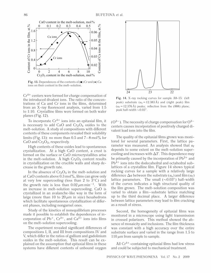
Cr4+ centers were formed for charge compensation ofthe introduced divalent ions. The ratio of the concen-trations of Ca and Cr ions in the films, determinedfrom an X-ray fluorescent analysis, varied from 1:5to 1:10. Crystalline films were formed on both waferplanes (Fig. 12).
To incorporate Cr4+ ions into an epitaxial film, itis necessary to add CaO and Cr2O3 oxides to themelt-solution. A study of compositions with differentcontents of these components revealed their solubilitylimits (Fig. 13): no more than 0.5 and 7−8 mol% forCaO and Cr2O3, respectively.
High contents of these oxides lead to spontaneouscrystallization. At a high CaO content, a crust isformed on the surface or CaO microcrystallites arisein the melt-solution. A high Cr2O3 content resultsin crystallization on the crucible walls and sharp de-crease in the growth rate.
In the absence of Cr2O3 in the melt-solution andat CaO contents above 0.3 mol%, films can grow onlyat very low supercooling (less than 2 to 3◦C) andthe growth rate is less than 0.02 μm min−1. Withan increase in melt-solution supercooling, CaO iscrystallized in an avalanche-like way in the form oflarge (more than 10 to 20 μm in size) hexahedronswhich facilitate spontaneous crystallization of differ-ent phases, including nongarnet ones.
Study of the kinetics of nonequilibrium processesmade it possible to establish the dependences of in-corporation of Pb+, Cr3+, and Ca2+ ions into filmson the melt-solution supercooling.
The experiment revealed significant differences ofcompositions I, II, and III from compositions IV andV, which differ in the ratios of gallium and gadoliniumoxides in the melt-solution. This result can be ex-plained on the assumption that epitaxial films in thesesystems have different contents of unbound oxygen
Fig. 14. X-ray rocking curves for sample A8-15: (leftpeak) substrate (as = 12.383 A) and (right peak) film(af = 12.376 A) peaks; reflection from the (888) plane;peak half-width ∼0.03◦.
(O2−). The necessity of charge compensation for O2−
centers causes incorporation of positively charged di-valent lead ions into the film.
The quality of the epitaxial films grown was moni-tored for several parameters. First, the lattice pa-rameter was measured. An analysis showed that af
depends to some extent on the melt-solution super-cooling and increases with ΔT . This dependence maybe primarily caused by the incorporation of Pb2+ andPb4+ ions into the dodecahedral and octahedral sub-lattices of a crystalline film. Figure 14 shows typicalrocking curves for a sample with a relatively largedifference Δa between the substrate (as) and film (af)lattice parameters. The small (∼0.03◦) half-widthof the curves indicates a high structural quality ofthe film grown. The melt-solution composition wasvaried to obtain a film−substrate lattice matchingup to the third decimal place. A larger differencebetween lattice parameters may lead to film crackingas a result of stress.
Second, the homogeneity of epitaxial films wasmonitored in a microscope using light transmissionin crossed polarizers. This method showed the ab-sence of mosaicity and inclusions. The film thicknesswas constant with a high accuracy over the entiresubstrate surface and varied in the range from 1.5 to110 μm from sample to sample.
All Cr4+-containing epitaxial films had low stressand could be subjected to mechanical treatment.
PHYSICS OF WAVE PHENOMENA Vol. 17 No. 2 2009
Nd3+:GGG AND Cr4+:GGG EPITAXIAL FILMS 87
Fig. 15. Absorption coefficients of different samplesof Cr, Ca:GGG/GGG epitaxial films (composition IV):A17-26 (film thickness 2h = 24 μm, tg = 1000◦C), A17-29 (2h = 25 μm, tg = 1005◦C), and A16-25 (2h = 65 μm,tg = 1008◦C). The inset shows the absorption spectrumof A16-25 in the near-IR region.
6. STUDY OF OPTICALAND LASING CHARACTERISTICS
OF Cr4+-CONTAINING FILMS
Cr4+ ions have broad absorption bands in the red(600−800 nm) and near-IR (about 1 μm) spectral re-gions. Annealing of bulk crystals in an oxygen atmo-sphere increases the intensity of these bands. The ab-sorption coefficient of Cr4+-containing crystals andepitaxial films depends on the annealing temperatureand atmosphere.
Along with the structural analysis, we investi-gated the absorption and luminescence spectra ofthe epitaxial films to determine the oxidation stateof chromium ions. The absorption and lumines-cence spectra were studied using a Shimadzu UV3101PC spectrophotometer and an ARC InSpectrumspectrofluorimeter, respectively. The absorption spec-tra contained complex bands. The measurements ofthe luminescence excitation spectra showed that thecomplex spectrum in the range from 600 to 800 μmcan be decomposed into components correspondingto the absorption bands of Cr3+ and Cr4+ ions. Inaddition, the absorption in epitaxial films that is due toCr ions, is summed with the additional absorption dueto the color centers formed as a result of incorporationof lead oxides into the film composition during growthfrom melt-solution. Thus, the absorption bands of Crions in a film are summed with the background of theso-called gray loss. During absorption saturation inCr4+-containing films, this background gives resid-ual absorption.
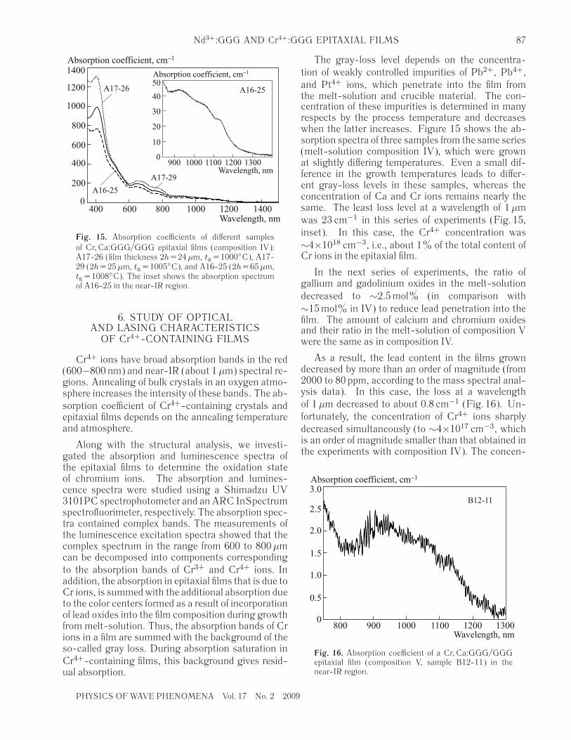
The gray-loss level depends on the concentra-tion of weakly controlled impurities of Pb2+, Pb4+,and Pt4+ ions, which penetrate into the film fromthe melt-solution and crucible material. The con-centration of these impurities is determined in manyrespects by the process temperature and decreaseswhen the latter increases. Figure 15 shows the ab-sorption spectra of three samples from the same series(melt-solution composition IV), which were grownat slightly differing temperatures. Even a small dif-ference in the growth temperatures leads to differ-ent gray-loss levels in these samples, whereas theconcentration of Ca and Cr ions remains nearly thesame. The least loss level at a wavelength of 1 μmwas 23 cm−1 in this series of experiments (Fig. 15,inset). In this case, the Cr4+ concentration was∼4×1018 cm−3, i.e., about 1% of the total content ofCr ions in the epitaxial film.
In the next series of experiments, the ratio ofgallium and gadolinium oxides in the melt-solutiondecreased to ∼2.5 mol% (in comparison with∼15 mol% in IV) to reduce lead penetration into thefilm. The amount of calcium and chromium oxidesand their ratio in the melt-solution of composition Vwere the same as in composition IV.
As a result, the lead content in the films growndecreased by more than an order of magnitude (from2000 to 80 ppm, according to the mass spectral anal-ysis data). In this case, the loss at a wavelengthof 1 μm decreased to about 0.8 cm−1 (Fig. 16). Un-fortunately, the concentration of Cr4+ ions sharplydecreased simultaneously (to ∼4×1017 cm−3, whichis an order of magnitude smaller than that obtained inthe experiments with composition IV). The concen-
Fig. 16. Absorption coefficient of a Cr, Ca:GGG/GGGepitaxial film (composition V, sample B12-11) in thenear-IR region.
PHYSICS OF WAVE PHENOMENA Vol. 17 No. 2 2009

88 BUFETOVA et al.
Table 4. Absorption saturation in the Cr4+-containing films
Sample Film Initial Residual Residual Absorption coefficientthickness transmittance transmittance loss δ, of Cr4+ ions,2h, μm T0 Tres cm−1 cm−1
A15-19 48 0.87 0.927 15.8 13.2A15-21 48.35 0.916 0.955 9.5 8.6
A15-22 32 0.91 0.966 10.8 18.7
A15-23 53.4 0.83 0.91 17.7 17.2
A16-25 65 0.83 0.91 14.5 14.2
A17-26 23.8 0.917 0.964 15.4 21
A17-27 39.1 0.88 0.922 20.7 12
A17-28 25.3 0.927 0.97 12.2 17.5
A17-29 25.6 0.914 0.98 8.7 26.3
trations of Cr and Ca ions in the film turned out to bethe same in both series of experiments.
Annealing of the samples obtained in these exper-iments showed that the Cr4+ concentration increasesduring annealing in oxygen, while the gray loss re-mains the same.
We measured the absorption saturation at a wave-length of 1 μm in the films grown. The experimentalsetup included a multimode Nd:YAG laser with diodepumping and passive Q-switching. A sample waslocated on the optical axis of the system behind thewaist of the probe laser beam. The sample couldbe moved along the axis and the laser pulse energydensity on the sample surface was a function of theelement coordinate on the optical axis. The diver-gence and diameter of the probe beam were about3 mrad and 2 mm, respectively. The pulse-repetitionfrequency at a pump power of 19 W was 11.76 kHz.Since the lifetime of a Cr4+ ion in the excited stateis 1.3 μs and the probe pulse width was 50 ns, the
Fig. 17. Dependences of the epitaxial film (sample A16-25) transmittance on the probe pulse energy density.
absorption saturation of Cr4+ ions in the films wasmeasured as a function of the energy density of theprobe pulse [32]. Figure 17 shows the dependenceof transmission of a gate cut from an epitaxial film(sample A16-25) on the energy density of the probepulse. The data obtained show that absorption issaturated in this film with a residual loss of about8%. The results for some other samples are listedin Table 4. The character of absorption saturationsuggests that the sample can be used as a Q-switch.
To reveal homogeneity of spectroscopic character-istics of the epitaxial films grown, we measured thesample transmission at low probe beam powers andsaturated absorption at a high power and a wave-length of 1 μm over the entire plane for a series ofchosen samples. Figure 18 shows the results ob-tained for sample A15-23. The measurements were
Fig. 18. Dependence of the transmittance of the epitaxialfilm (sample A15-23) (1) at low probe beam powers and(2) at absorption saturation on the transverse scanningcoordinate X (the points X = 0 and 38 mm correspond tothe sample edge and center, respectively).
PHYSICS OF WAVE PHENOMENA Vol. 17 No. 2 2009

Nd3+:GGG AND Cr4+:GGG EPITAXIAL FILMS 89
Fig. 19. Time dependence of the multimode lasing of apassive Q-switch laser based on a Cr4+:GGG epitaxialfilm at a large excess above the threshold pump power.
performed at several points along the sample diame-ter (the measurement direction coincides with the Xcoordinate axis in the plot). The points X = 0 and38 mm correspond to the sample edge and center,respectively. The measurement error was about 1%.This study showed a high homogeneity of the epitaxialfilms.
To analyze the possibility of using chromium-containing epitaxial films as passive gates, a sam-ple was mounted in the cavity of a diode-pumpedNd:YAG laser at the Brewster angle. The exper-imental film samples were not additionally treated(after growth) and no antireflection coatings weredeposited on them. The experimental conditionswere as follows: laser pulse width 500−800 ns, pulserepetition frequency ∼100 kHz, and radiation power∼0.5 W at a pump power of 7 W. When the laseroperated near the threshold pump power, the TEM00
Fig. 20. Combined (microchip) LPE-grown Cr4+:GGG/Nd3+:GGG active element.
Fig. 21. TEM00-lasing pulse of a laser based on on thecombined Q-switched active element (Fig. 20).
mode was generated with a highly stable amplitudeof giant pulses and their repetition frequency. Asignificant excess above the lasing threshold led togeneration of other modes, which affected the shapeof laser pulse and its amplitude stability (Fig. 19).
To design an active element of a compact (mi-crochip) laser, we deposited a Cr4+-containing epi-taxial film on active Nd:GGG elements ∅ 6.3×10 mmin size.
The results of this experiment showed that thesurface of an active element must be specially pro-cessed (using superfine polishing or ion etching) toremove the damaged layer. In addition, it is nec-essary to change the billet rotation rate during filmdeposition because of the change in the hydrody-namic conditions of substrate washing by the melt-solution, which is caused by the change in the billetdiameter in comparison with the developed process(6.3 mm instead of 76 mm). All conditions satisfied,we obtained Cr4+:GGG/Nd:GGG active elements(Fig. 20). Installment of these elements in the cavityof the diode-pumped laser yielded single-mode lasingin the Q-switched mode. The laser pulse width wasabout 350 ns in this case (Fig. 21).
7. CONCLUSIONS
A technique for growing Nd:GGG epitaxial filmson undoped 76-mm GGG substrates have been de-veloped. The spectral luminescence characteristicsof the films completely coincide with those of bulkcrystals.
A technique of LPE of single-crystal Cr4+:GGGfilms on undoped GGG substrates and on substratesdoped with Nd3+ ions has been developed. The sub-strates were 30−76 mm or 5−8 mm in diameter. It is
PHYSICS OF WAVE PHENOMENA Vol. 17 No. 2 2009

90 BUFETOVA et al.
shown that this technique makes it possible to obtainfilms with a crystalline structure and characteristicsvery close to those of single crystals grown by theCzochralski method. The growth conditions andmelt-solution compositions are determined, whichallowed us to obtain epitaxial films with high con-centrations of Cr4+ ions (up to 5×1018 cm−3) andsmall loss at a wavelength of 1 μm. It is shown thatthe grown Cr4+-containing garnet films can be usedas passive Q-switches for 1-μm lasers. The sam-ples have an acceptable gray-loss level, which makespossible further improvement of their parameters byannealing at different temperatures in atmospheres ofdifferent composition.
REFERENCES
1. T. Y. Fan and R. L. Byer, “Diode Laser-PumpedSolid-State Lasers,” IEEE J. Quantum Electron. 24,895 (1988).
2. S. C. Tidwell, J. F. Seamans, M. S. Bowers, andA. K. Cousins, “Scaling CW Diode-End-PumpedNd:YAG Lasers to High Average Powers,” IEEE J.Quantum Electron. 28, 997 (1992).
3. P. J. Hardman, W. A. Clarkson, and D. C. Hanna, “Ef-ficient Operation of an Acousto-Optically-InducedUnidirectional and Single-Frequency Q-SwitchedNd:YLF Ring Laser,” in OSA TOPS. AdvancedSolid-State Lasers, Ed. by M. M. Feier, H. Injeyan,and U. Keller (Washington, Opt. Soc. Amer., 1999).Vol. 26, p. 236.
4. J. J. Zayhowski, “Microchip Lasers,” Opt. Mater. 11,255 (1999).
5. B. D. Sinclair, “Frequency-Doubled MicrochipLasers,” Opt. Mater. 11, 217 (1999).
6. A. Giesen, H. Hugel, A. Voss, K. Wittig, U. Brauch,and H. Opower, “Scalable Concept for Diode-Pumped High-Power Solid-State Lasers,” Appl.Phys. B. 58, 365 (1994).
7. I. Melngailis, W. E. Keicher, C. Freed, S. Marcus,B.E. Edwards, A. Sanchez, T.Y. Fan, and D.L. Spears,“Laser Radar Component Technology,” Proc. IEEE.84(2), 227 (1996).
8. P. Loosen, “Advanced Concepts of Using DiodeLasers in Materials Processing,” Proc. SPIE. 3097,480 (1997).
9. M. M. Abreu, R. A. Sierra, and P. A. Netland, “DiodeLaser-Pumped, Frequency-Doubled Nd:YAG LaserPeripheral Iridotomy,” Opthalmic Surgery andLasers. 28, 305 (1997).
10. W. Koechner, Solid State Laser Engineering(Springer-Verlag, Berlin, 1996).
11. J. M. Eggleston, T. J. Kane, K. Kuhn, J. Unternahrer,and R. L. Byer, “The Slab Geometry Laser. Part 1:Theory,” IEEE J. Quantum Electron. 20, 289 (1984).
12. J. P. van der Ziel, W. A. Bonner, L. Kopf, S. Singh, andL. G. Van Uitert, “Laser Oscillation from Ho3+ andNd3+ Ions in Epitaxially Grown Thin Aluminum Gar-net Films,” Appl. Phys. Lett. 22, 656 (1973).
13. J. G. Grabmaier, R. D. Plattner, P. Mockel, andW. W. Kruhler, “Liquid Phase Epitaxy of Nd3+-Doped YAG Layers by Dipping Technique,” J. Cryst.Growth. 34, 280 (1976).
14. D. S. Gill, A. A. Anderson, R. W. Eason, T. J. War-burton, and D. P. Shepherd, “Laser Operation of aNd:Gd3Ga5O12 Thin-Film Optical Waveguide Fabri-cated by Pulsed Laser Deposition,” Appl. Phys. Lett.69, 10 (1996).
15. M. Hempstead, J. S. Wilkinson, and L. Reekie,“Waveguide Lasers Operating at 1084 nm inNeodymium-Diffused Lithium Niobate,” IEEEPhoton. Tech. Lett. 4, 852 (1992).
16. A. C. Tropper, “Laser Crystal Waveguides,” Laser undOptroelektron. 27(4), 57 (1995).
17. P. R. Willmott, P. Manoravi, and K. Holliday, “Pro-duction and Characterization of Nd, Cr:GSGG ThinFilms on Si(001) Grown by Pulsed Laser Ablation,”Appl. Phys. A. 70(4), 425 (2000).
18. G. R. Bay, H. L. M. Chang, and C. M. Foster, “Prepa-ration of Single-Crystal Y3Al5O12 Thin Film by Met-alorganic Chemical Vapor Deposition,” Appl. Phys.Lett. 64, 1777 (1994).
19. M. Shimokozono, N. Sugimoto, A. Tate, Y. Katoh,M. Tanno, S. Fukuda, and T. Ryuoh, “Room-Tempe-rature Operation of an Yb-Doped Gd3Ga5O12 BuriedChannel Waveguide Laser at 1.025μm Wavelength,”Appl. Phys. Lett. 68, 2177 (1996).
20. V. V. Randoshkin, A. M. Belovolov, M. I. Belovolov,N. V. Vasil’eva, E. M. Dianov, K. V. Stashun, andM. I. Timoshechkin, “Growth and Luminescence ofEpitaxial Yb0.3ErxGd2.7−xGa5O12 Films,” QuantumElectron. 28(3), 225 (1998).
21. H. Kumagai, K. Adachi, M. Ezaki, K. Toyoda, andM. Obara, “Epitaxial Growth of Nd:YAG Thin Filmsby Pulsed Laser Deposition,” Appl. Surf. Sci. 109,528 (1997).
22. D. Pelenc, B. Chambaz, I. Chartier, B. Ferrand,C. Wyon, D. P. Shepherd, D. C. Hanna, A. C. Large,and A. C. Tropper, “High Slope Efficiency and LowThreshold in a Diode-Pumped Epitaxially GrownYb:YAG Waveguide Laser,” Opt. Commun. 115, 491(1995).
23. N. B. Angert, N. I. Borodin, V. M. Garmash,V. A. Zhitnyuk, A. G. Okhrimchuk, O. G. Siyuchen-ko, and A. V. Shestakov, “Lasing Due to ImpurityColor Centers in Yttrium Aluminum Garnet Crystalsat Wavelengths in the Range 1.35−1.45 μm,” Sov. J.Quantum Electron. 18, 73 (1988).
24. B. Henderson, H. G. Gallagher, T. P. J. Han, andM. A. Scott, “Optical Spectroscopy and OptimalCrystal Growth of Some Cr4+-Doped Garnets,”J. Phys. Condens. Matter. 12(8), 1927 (2000).
PHYSICS OF WAVE PHENOMENA Vol. 17 No. 2 2009

Nd3+:GGG AND Cr4+:GGG EPITAXIAL FILMS 91
25. A. G. Okhrimchuk and A. V. Shestakov, “Absorp-tion Saturation Mechanism for YAG:Cr4+ Crystals,”Phys. Rev. B. 61, 988 (2000).
26. V. B. Tsvetkov, I. A. Shcherbakov, A. V. Shestakov,and I. A. Ivanov, “Influence of Excited State Absorp-tion to the Residual Losses and Q-Switch Operationof Nd-Lasers with Saturable Absorbers Doped byCr4+-Ions,” in OSA TOPS. Advanced Solid-StateLasers, Ed. by Chr. Marshall (Washington, D.C.,Opt. Soc. Amer., 2001). Vol. 50, p. 568.
27. R. Feldman, Y. Shimony, and Z. Burshtein,“Chromium Ion Valence Transformations in Cr,Ca:YAG used for passive Q-switching,” Proc. SPIE.4970, 61 (2003).
28. S. B. Ubizskii, I. M. Syvorotka, S. S. Melnyk,A. O. Matkovskii, K. Kopczynski, Z. Mierczyk,and Z. Frukacz, “Growth and Characterization ofYAG:Cr4+ Epitaxial Films,” Proc. SPIE. 3724, 353(1999).
29. R. Haibo, C. Jianbo, H. Zonglin, G. Tao, and G. Hua-rong, “The Growth and Absorption Characterizationof Cr, Ca:YAG by Liquid-Phase Epitaxy,” J. CrystalGrowth. 236(1), 191 (2002).
30. S. L. Blank, J. W. Nielsen, and W. A. Biolsi, “Prepa-ration and Properties of Magnetic Garnet FilmsContaining Divalent and Tetravalent Ions,” J. Elec-trochem. Soc. 123, 856 (1976).
31. W. F. Krupke, M. D. Shinn, J. E. Marion, J. A. Caird,and S. E. Stokowski, “Spectroscopic, Optical, andThermomechanical Properties of Neodymium- andChromium-Doped Gadolinium Scandium GalliumGarnets,” J. Opt. Soc. Amer. B. 3(1), 102 (1986).
32. V. B. Tsvetkov, G. A. Bufetova, D. A. Nikolaev,V. F. Seregin, I. A. Shcherbakov, M.Yu. Gusev, andI. A. Ivanov, “Cr4+:GGG Epitaxial Films for Solid-State Lasers,” Laser Phys. 15(4), 579 (2005).
PHYSICS OF WAVE PHENOMENA Vol. 17 No. 2 2009
Related Documents


