NCT5577D Nuvoton LPC I/O Date: April 13 th , 2011 Revision 1.1

Welcome message from author
This document is posted to help you gain knowledge. Please leave a comment to let me know what you think about it! Share it to your friends and learn new things together.
Transcript

NCT5577D Nuvoton LPC I/O
Date: April 13th, 2011 Revision 1.1
NCT5577D
Publication Release Date: April 13, 2011 -I- Version: 1.1
Table of Contents – 1. GENERAL DESCRIPTION ......................................................................................................... 1 2. FEATURES ................................................................................................................................. 2 3. BLOCK DIAGRAM ...................................................................................................................... 5 4. PIN LAYOUT............................................................................................................................... 6 5. PIN DESCRIPTION..................................................................................................................... 7
5.1 LPC Interface .................................................................................................................. 8 5.2 Serial Port Interface ........................................................................................................ 8 5.3 KBC Interface.................................................................................................................. 8 5.4 CIR Interface................................................................................................................... 9 5.5 Hardware Monitor Interface ............................................................................................ 9 5.6 Intel® PECI Interface .................................................................................................... 10 5.7 Advanced Configuration & Power Interface.................................................................. 10 5.8 Advanced Sleep State Control...................................................................................... 10 5.9 SMBus Interface ........................................................................................................... 11 5.10 Power Pins.................................................................................................................... 11 5.11 AMD Power-On Sequence ........................................................................................... 11 5.12 AMD SB-TSI Interface .................................................................................................. 12 5.13 Dual Voltage Control..................................................................................................... 12 5.14 DSW.............................................................................................................................. 12 5.15 IR .................................................................................................................................. 12 5.16 General Purpose I/O Port ............................................................................................. 13
5.16.1 GPIO-2 Interface .......................................................................................................................13 5.16.2 GPIO-3 Interface .......................................................................................................................13 5.16.3 GPIO-4 Interface .......................................................................................................................14 5.16.4 GPIO-5 Interface .......................................................................................................................14 5.16.5 GPIO-7 Interface .......................................................................................................................14 5.16.6 GPIO-8 Interface .......................................................................................................................15 5.16.7 GPIO-9 Interface .......................................................................................................................16 5.16.8 GPIO-A Interface .......................................................................................................................16
5.17 Strapping Pins............................................................................................................... 16 5.18 Internal pull-up, pull-down pins ..................................................................................... 17
6. GLUE LOGIC ............................................................................................................................ 18 6.1 ACPI Glue Logic ........................................................................................................... 18 6.2 BKFD_CUT & LATCH_BKFD_CUT.............................................................................. 20 6.3 PSON# Block Diagram ................................................................................................. 21 6.4 PWROK ........................................................................................................................ 22 6.5 Front Panel LEDs.......................................................................................................... 23
6.5.1 Automatic Mode ..........................................................................................................................23 6.5.2 Manual Mode ..............................................................................................................................24 6.5.3 S0~S5 LED Blink Block Diagram ................................................................................................25 6.5.4 LED Pole (LED_POL ) ................................................................................................................25 6.5.5 Deeper Sleeping State Detect Function ......................................................................................26
6.6 Advanced Sleep State Control (ASSC) Function ......................................................... 28 6.6.1 When ASSC is disabled ..............................................................................................................28 6.6.2 When ASSC is enabled (Enter into Deeper Sleeping State) .......................................................28 6.6.3 When ASSC is enabled (Exit Deeper Sleeping State) ................................................................29

NCT5577D
Publication Release Date: April 13, 2011 -II- Version: 1.1
6.7 Intel DSW Function....................................................................................................... 30 6.7.1 Enter DSW State timing diagram ................................................................................................30 6.7.2 Exit DSW State timing diagram...................................................................................................31
6.8 AMD Power-On Sequence ........................................................................................... 32 7. CONFIGURATION REGISTER ACCESS PROTOCOL ........................................................... 35
7.1 Configuration Sequence ............................................................................................... 37 7.1.1 Enter the Extended Function Mode.............................................................................................37 7.1.2 Configure the Configuration Registers ........................................................................................37 7.1.3 Exit the Extended Function Mode ...............................................................................................38 7.1.4 Software Programming Example.................................................................................................38
8. HARDWARE MONITOR ........................................................................................................... 39 8.1 General Description ...................................................................................................... 39 8.2 Access Interfaces.......................................................................................................... 39 8.3 LPC Interface ................................................................................................................ 39 8.4 I2C interface .................................................................................................................. 41 8.5 Analog Inputs ................................................................................................................ 42
8.5.1 Voltages Over 2.048 V or Less Than 0 V....................................................................................43 8.5.2 Voltage Data Format ...................................................................................................................43 8.5.3 Temperature Data Format...........................................................................................................44
8.6 PECI.............................................................................................................................. 47 8.7 Fan Speed Measurement and Control ......................................................................... 49
8.7.1 Fan Speed Reading ....................................................................................................................49 8.7.2 Fan Speed Calculation by Fan Count Reading ...........................................................................49 8.7.3 Fan Speed Calculation by Fan RPM Reading.............................................................................49 8.7.4 Fan Speed Control ......................................................................................................................49 8.7.5 SMART FANTM Control ...............................................................................................................50 8.7.6 Temperature Source & Reading for Fan Control.........................................................................50
8.8 SMART FANTM I ............................................................................................................ 51 8.8.1 Thermal Cruise Mode..................................................................................................................51 8.8.2 Speed Cruise Mode ....................................................................................................................52
8.9 SMART FANTM IV & Close Loop Fan Control Mode..................................................... 54 8.9.1 Step Up Time / Step Down Time.................................................................................................57 8.9.2 Fan Output Start-up Value ..........................................................................................................57 8.9.3 Fan Output Stop Value................................................................................................................57 8.9.4 Fan Output Stop Time.................................................................................................................58 8.9.5 Fan Output Step..........................................................................................................................58 8.9.6 Revolution Pulse Selection..........................................................................................................58 8.9.7 Weight Value Control ..................................................................................................................59
8.10 Alert and Interrupt ......................................................................................................... 60 8.10.1 SMI# Interrupt Mode..................................................................................................................61 8.10.2 Voltage SMI# Mode ...................................................................................................................61 8.10.3 Fan SMI# Mode .........................................................................................................................61 8.10.4 Temperature SMI# Mode...........................................................................................................61 8.10.5 OVT# Interrupt Mode.................................................................................................................66
8.11 Power Measurement..................................................................................................... 67 9. HARDWARE MONITOR REGISTER SET................................................................................ 69
9.1 Address Port (Port x5h) ................................................................................................ 69 9.2 Data Port (Port x6h)...................................................................................................... 69

NCT5577D
Publication Release Date: April 13, 2011 -III- Version: 1.1
9.3 SYSFANOUT PWM Output Frequency Configuration Register – Index 00h (Bank 0) 69 9.4 SYSFANOUT Output Value Select Register – Index 01h (Bank 0).............................. 70 9.5 CPUFANOUT PWM Output Frequency Configuration Register – Index 02h (Bank 0) 71 9.6 CPUFANOUT Output Value Select Register – Index 03h (Bank 0) ............................. 72 9.7 SYSFANOUT Configuration Register I – Index 04h (Bank 0) ...................................... 72 9.8 Reserved Register – Index 05h ~ 0Fh (Bank 0) ........................................................... 73 9.9 Reserved Register – Index 10h (Bank 0) ..................................................................... 73 9.10 Reserved Register – Index 11h (Bank 0) ..................................................................... 73 9.11 Reserved Register – Index 12-17h (Bank 0) ................................................................ 73 9.12 OVT# Configuration Register – Index 18h (Bank 0) ..................................................... 73 9.13 Reserved Registers – Index 19h ~ 1Fh (Bank 0) ......................................................... 73 9.14 Value RAM ⎯ Index 20h ~ 3Fh (Bank 0) ..................................................................... 73 9.15 Configuration Register – Index 40h (Bank 0) ............................................................... 74 9.16 Interrupt Status Register 1 – Index 41h (Bank 0) ......................................................... 75 9.17 Interrupt Status Register 2 – Index 42h (Bank 0) ......................................................... 75 9.18 SMI# Mask Register 1 – Index 43h (Bank 0)................................................................ 76 9.19 SMI# Mask Register 2 – Index 44h (Bank 0)................................................................ 76 9.20 Interrupt Status Register 4 – Index 45h (Bank 0) ......................................................... 77 9.21 SMI# Mask Register 3 – Index 46h (Bank 0)................................................................ 77 9.22 Reserved Register – Index 47h (Bank 0) ..................................................................... 78 9.23 Serial Bus Address Register – Index 48h (Bank 0) ...................................................... 78 9.24 Reserved Register – Index 49h ~ 4Ah (Bank 0)........................................................... 78 9.25 SMI/OVT Control Register1 – Index 4Ch (Bank 0)....................................................... 78 9.26 FAN IN/OUT Control Register – Index 4Dh (Bank 0) ................................................... 79 9.27 Bank Select Register – Index 4Eh (Bank 0) ................................................................. 79 9.28 Nuvoton Vendor ID Register – Index 4Fh (Bank 0) ...................................................... 80 9.29 Reserved Register – Index 50h ~ 57h (Bank 0) ........................................................... 80 9.30 Chip ID – Index 58h (Bank 0) ....................................................................................... 80 9.31 Reserved Register – Index 5Ah ~ 5Ch (Bank 0) .......................................................... 80 9.32 VBAT Monitor Control Register – Index 5Dh (Bank 0) ................................................. 81 9.33 Current Mode Enable Register – Index 5Eh (Bank 0) .................................................. 81 9.34 Reserved Register – Index 5F (Bank 0) ....................................................................... 82 9.35 PORT 80 DATA INPUT Register – Index 60 (Bank 0) ................................................. 82 9.36 Reserved Register – Index 61F ~ 62F (Bank 0) ........................................................... 82 9.37 FANOUT MAX RPM Detect Time Register – Index 65 (Bank 0).................................. 82 9.38 MAX RPM Detect Time Configuration Register – Index 66 (Bank 0) ........................... 82 9.39 Reserved register – Index 67h ~ 72h (Bank 0)............................................................. 83 9.40 MONITOR TEMPERATURE 1 Register (Integer Value)- Index 73h (Bank 0) ............. 83 9.41 MONITOR TEMPERATURE 1 Register (Fractional Value)- Index 74h (Bank 0)......... 83 9.42 MONITOR TEMPERATURE 2 Register (Integer Value)- Index 75h (Bank 0) ............. 83 9.43 MONITOR TEMPERATURE 2 Register (Fractional Value)- Index 76h (Bank 0)......... 84 9.44 Reserved Register - Index 77h (Bank 0) ...................................................................... 84 9.45 Reserved Register - Index 78h (Bank 0) ...................................................................... 84 9.46 Reserved Register – Index 79h~ADh (Bank 0) ............................................................ 84 9.47 PECI Temperature Reading Enable for SMIOVT and SMART FAN Control Register – Index AEh (Bank 0) ......................................................................................................................... 84 9.48 BEEP Control Register 1 – Index B2h (Bank0) ............................................................ 84

NCT5577D
Publication Release Date: April 13, 2011 -IV- Version: 1.1
9.49 BEEP Control Register 2 – Index B3h (Bank0) ............................................................ 85 9.50 BEEP Control Register 3 – Index B4h (Bank0) ............................................................ 86 9.51 BEEP Control Register 4 – Index B5h (Bank0) ............................................................ 86 9.52 SYSFAN Monitor Temperature Source Select Register/ STOPDUTY Enable Register – Index 00h (Bank 1) .......................................................................................................................... 87 9.53 SYSFAN Target Temperature Register / SYSFANIN Target Speed_L Register – Index 01h (Bank 1).................................................................................................................................... 88 9.54 SYSFAN MODE Register / SYSFAN TOLERRANCE Register – Index 02h (Bank 1). 88 9.55 SYSFANOUT Step Up Time Register – Index 03h (Bank 1)........................................ 89 9.56 SYSFANOUT Step Down Time Register – Index 04h (Bank 1) ................................... 89 9.57 SYSFANOUT Stop Value Register – Index 05h (Bank 1) ............................................ 89 9.58 SYSFANOUT Start-up Value Register – Index 06h (Bank 1)....................................... 90 9.59 SYSFANOUT Stop Time Register – Index 07h (Bank 1) ............................................. 90 9.60 Reserved Register – Index 08h (Bank 1) ..................................................................... 90 9.61 SYSFANOUT Output Value Select Register – Index 09h (Bank 1).............................. 90 9.62 SYSFANIN Tolerance_H / Target Speed_H Register – Index 0Ch (Bank 1) ............... 91 9.63 Reserved Register – Index 0Dh (Bank 1)..................................................................... 91 9.64 SMART FAN IV SYSFANOUT STEP Register – Index 20h (Bank 1) .......................... 91 9.65 SYSFAN (SMART FANTM IV) Temperature 1 Register(T1) – Index 21h (Bank 1)....... 91 9.66 SYSFAN (SMART FANTM IV) Temperature 2 Register(T2) – Index 22h (Bank 1)....... 92 9.67 SYSFAN (SMART FANTM IV) Temperature 3 Register(T3) – Index 23h (Bank 1)....... 92 9.68 SYSFAN (SMART FANTM IV) Temperature 4 Register(T4) – Index 24h (Bank 1)....... 92 9.69 SYSFAN (SMART FANTM IV) DC/PWM 1 Register – Index 27h (Bank 1) ................... 92 9.70 SYSFAN (SMART FANTM IV) DC/PWM 2 Register – Index 28h (Bank 1) ................... 93 9.71 SYSFAN (SMART FANTM IV) DC/PWM 3 Register – Index 29h (Bank 1) ................... 93 9.72 SYSFAN (SMART FANTM IV) DC/PWM 4 Register – Index 2Ah (Bank 1)................... 93 9.73 Reserved Register – Index 2Bh~30h (Bank 1) ............................................................. 93 9.74 SYSFAN 3-Wire Enable Register – Index 31h (Bank 1) .............................................. 94 9.75 Reserved Register – Index 32h ~ 34h(Bank 1) ............................................................ 94 9.76 SYSFAN (SMART FANTM IV) Temperature Critical Register(TR) – Index 35h (Bank 1) 94 9.77 Reserved Register – Index 36h ~ 37h (Bank 1) ........................................................... 94 9.78 SYSFANOUT Critical Temperature Tolerance Register – Index 38h (Bank 1)............ 94 9.79 Weight value Configuration Register – Index 39h (Bank 1) ......................................... 95 9.80 SYSFANOUT Temperature Step Register – Index 3Ah (Bank 1) ................................ 95 9.81 SYSFANOUT Temperature Step Tolerance Register – Index 3Bh (Bank 1) ............... 96 9.82 SYSFANOUT Weight Step Register – Index 3Ch (Bank 1) ......................................... 96 9.83 SYSFANOUT Temperature Base Register – Index 3Dh (Bank 1) ............................... 96 9.84 SYSFANOUT Temperature Fan Duty Base Register – Index 3Eh (Bank 1)................ 96 9.85 Reserved Register – Index 3Fh (Bank 1) ..................................................................... 97 9.86 Reserved Register – Index 40h (Bank 1) ..................................................................... 97 9.87 Reserved Register – Index 41h (Bank 1) ..................................................................... 97 9.88 Reserved Register – Index 42h ~ 44h (Bank 1) ........................................................... 97 9.89 SYSFAN Maximum RPM (Low Byte) Register – Index 45h (Bank 1) .......................... 97 9.90 SYSFAN Maximum RPM (High Byte) Register – Index 46h (Bank 1).......................... 97 9.91 Reserved Register – Index 49h ~ 4Fh (Bank1) ............................................................ 97 9.92 SMIOVT2 Temperature Source (High Byte) Register – Index 50h (Bank 1)................ 97

NCT5577D
Publication Release Date: April 13, 2011 -V- Version: 1.1
9.93 SMIOVT2 Temperature Source (Low Byte) Register – Index 51h (Bank 1)................. 98 9.94 SMIOVT2 Temperature Source Configuration Register – Index 52h (Bank 1) ............ 98 9.95 SMIOVT2 Temperature Source Hysteresis (High Byte) Register – Index 53h (Bank 1) 98 9.96 SMIOVT2 Temperature Source Hysteresis (Low Byte) Register – Index 54h (Bank 1)99 9.97 SMIOVT2 Temperature Source Over-temperature (High Byte) Register – Index 55h (Bank1) 99 9.98 SMIOVT2 Temperature Source Over-temperature (Low Byte) Register – Index 56h (Bank 1) 99 9.99 Reserved Register – Index 57h ~ 7Fh (Bank 1) ......................................................... 100 9.100 CPUFAN Monitor Temperature Source Select Register/ STOPDUTY Enable Register – Index 00h (Bank 2) ........................................................................................................................ 100 9.101 CPUFAN Target Temperature Register / CPUFANIN Target Speed_L Register – Index 01h (Bank 2).................................................................................................................................. 101 9.102 CPUFAN MODE Register / CPUFAN TOLERRANCE Register – Index 02h (Bank 2) 101 9.103 CPUFANOUT Step Up Time Register – Index 03h (Bank 2) ..................................... 101 9.104 CPUFANOUT Step Down Time Register – Index 04h (Bank 2)................................. 102 9.105 CPUFANOUT Stop Value Register – Index 05h (Bank 2).......................................... 102 9.106 CPUFANOUT Start-up Value Register – Index 06h (Bank 2) .................................... 102 9.107 CPUFANOUT Stop Time Register – Index 07h (Bank 2) ........................................... 103 9.108 Reserved Register – Index 08h (Bank 2) ................................................................... 103 9.109 CPUFANOUT Output Value Select Register – Index 09h (Bank 2) ........................... 103 9.110 CPUFANIN Tolerance_H / Target Speed_H Register – Index 0Ch (Bank 2)............. 103 9.111 Reserved Register – Index 0Dh (Bank 2)................................................................... 104 9.112 SMART FAN IV CPUFANOUT STEP Register – Index 20h (Bank 2)........................ 104 9.113 CPUFAN (SMART FANTM IV) Temperature 1 Register(T1) – Index 21h (Bank 2)..... 104 9.114 CPUFAN (SMART FANTM IV) Temperature 2 Register(T2) – Index 22h (Bank 2)..... 104 9.115 CPUFAN (SMART FANTM IV) Temperature 3 Register(T3) – Index 23h (Bank 2)..... 105 9.116 CPUFAN (SMART FANTM IV) Temperature 4 Register(T4) – Index 24h (Bank 2)..... 105 9.117 CPUFAN (SMART FANTM IV) DC or DUTY_SMF4 PWM1 Register – Index 27h (Bank 2) 105 9.118 CPUFAN (SMART FANTM IV) DC or DUTY_SMF4 PWM2 Register – Index 28h (Bank 2) 105 9.119 CPUFAN (SMART FANTM IV) DC or DUTY_SMF4 PWM3 Register – Index 29h (Bank 2) 106 9.120 CPUFAN (SMART FANTM IV) DC or DUTY_SMF4 PWM4 Register – Index 2Ah (Bank 2) 106 9.121 Reserved Register – Index 2Dh~ 30h (Bank 2)......................................................... 106 9.122 CPUFAN 3-Wire FAN Enable Register – Index 31h (Bank 2).................................... 106 9.123 Reserved Register – Index 32h ~ 34h(Bank 2) .......................................................... 106 9.124 CPUFAN (SMART FANTM IV) Temperature Critical Register(TR) – Index 35h (Bank 2) 107 9.125 Reserved Register – Index 36h ~ 37h (Bank 2) ......................................................... 107 9.126 CPUFANOUT Critical Temperature Tolerance Register – Index 38h (Bank 2).......... 107 9.127 Weight value Configuration Register – Index 39h (Bank 2) ....................................... 107 9.128 CPUFANOUT Temperature Step Register – Index 3Ah (Bank 2).............................. 108 9.129 CPUFANOUT Temperature Step Tolerance Register – Index 3Bh (Bank 2)............. 108 9.130 CPUFANOUT Weight Step Register – Index 3Ch (Bank 2) ....................................... 109

NCT5577D
Publication Release Date: April 13, 2011 -VI- Version: 1.1
9.131 CPUFANOUT Temperature Base Register – Index 3Dh (Bank 2)............................. 109 9.132 CPUFANOUT Temperature Fan Duty Base Register – Index 3Eh (Bank 2) ............. 109 9.133 Reserved Register – Index 3Fh (Bank 2) ................................................................... 109 9.134 Reserved Register – Index 40h (Bank 2) ................................................................... 109 9.135 Reserved Register – Index 41h (Bank 2) ................................................................... 109 9.136 Reserved Register – Index 42h ~ 44h (Bank 2) ......................................................... 109 9.137 CPUFAN Maximum RPM (Low Byte) Register – Index 45h (Bank 2) ........................ 110 9.138 CPUFAN Maximum RPM (High Byte) Register – Index 46h (Bank 2) ....................... 110 9.139 Reserved Register – Index 49h ~ 4Fh (Bank2) .......................................................... 110 9.140 SMIOVT3 Temperature Source (High Byte) Register – Index 50h (Bank 2).............. 110 9.141 SMIOVT3 Temperature Source (Low Byte) Register – Index 51h (Bank 2)............... 110 9.142 SMIOVT3 Temperature Source Configuration Register – Index 52h (Bank 2) .......... 111 9.143 SMIOVT3 Temperature Source Hysteresis (High Byte) Register – Index 53h (Bank 2) 111 9.144 SMIOVT3 Temperature Source Hysteresis (Low Byte) Register – Index 54h (Bank 2) 111 9.145 SMIOVT3 Temperature Source Over-temperature (High Byte) Register – Index 55h (Bank 2) 112 9.146 SMIOVT3 Temperature Source Over-temperature (Low Byte) Register – Index 56h (Bank 2) 112 9.147 Reserved Register – Index 57h ~ 7Fh (Bank 2) ......................................................... 112 9.148 Reserved Register – Index 00h (Bank 3) ................................................................... 112 9.149 Reserved Register – Index 01h (Bank 3) ................................................................... 112 9.150 Reserved Register – Index 02h (Bank 3) ................................................................... 112 9.151 Reserved Register – Index 03h (Bank 3) ................................................................... 112 9.152 Reserved Register – Index 04h (Bank 3) ................................................................... 112 9.153 Reserved Register – Index 05h (Bank 3) ................................................................... 112 9.154 Reserved Register – Index 06h (Bank 3) ................................................................... 113 9.155 Reserved Register – Index 07h (Bank 3) ................................................................... 113 9.156 Reserved Register – Index 08h (Bank 3) ................................................................... 113 9.157 Reserved Register – Index 09h (Bank 3) ................................................................... 113 9.158 Reserved Register – Index 0Ch (Bank 3)................................................................... 113 9.159 Reserved Register – Index 0Dh (Bank 3)................................................................... 113 9.160 Reserved Register – Index 20h (Bank 3) ................................................................... 113 9.161 Reserved Register – Index 21h (Bank 3) ................................................................... 113 9.162 Reserved Register – Index 22h (Bank 3) ................................................................... 113 9.163 Reserved Register – Index 23h (Bank 3) ................................................................... 113 9.164 Reserved Register – Index 24h (Bank 3) ................................................................... 113 9.165 Reserved Register – Index 27h (Bank 3) ................................................................... 113 9.166 Reserved Register – Index 28h (Bank 3) ................................................................... 113 9.167 Reserved Register – Index 29h (Bank 3) ................................................................... 113 9.168 Reserved Register – Index 2Ah (Bank 3) ................................................................... 113 9.169 Reserved Register – Index Index 2Dh~ 30h (Bank 3)................................................ 113 9.170 Reserved Register – Index 31h (Bank 3) ................................................................... 113 9.171 Reserved Register – Index 32h ~ 34h(Bank 3) .......................................................... 113 9.172 Reserved Register – Index 35h (Bank 3) ................................................................... 113 9.173 Reserved Register – Index 36h ~ 37h (Bank 3) ......................................................... 113
NCT5577D
Publication Release Date: April 13, 2011 -VII- Version: 1.1
9.174 Reserved Register – Index 38h (Bank 3) ................................................................... 113 9.175 Reserved Register – Index 39h (Bank 3) ................................................................... 114 9.176 Reserved Register – Index 3Ah (Bank 3) ................................................................... 114 9.177 Reserved Register – Index 3Bh (Bank 3) ................................................................... 114 9.178 Reserved Register – Index 3Ch (Bank 3)................................................................... 114 9.179 Reserved Register – Index 3Dh (Bank 3)................................................................... 114 9.180 Reserved Register – Index 3Eh (Bank 3) ................................................................... 114 9.181 Reserved Register – Index 3Fh (Bank 3) ................................................................... 114 9.182 Reserved Register – Index 40h (Bank 3) ................................................................... 114 9.183 Reserved Register – Index 41h (Bank 3) ................................................................... 114 9.184 Reserved Register – Index 42h ~ 44h (Bank 3) ......................................................... 114 9.185 Reserved Register – Index 45h (Bank 3) ................................................................... 114 9.186 Reserved Register – Index 46h (Bank 3) ................................................................... 114 9.187 Reserved Register – Index 49h ~ 7Fh (Bank3) .......................................................... 114 9.188 PCH_CHIP_CPU_MAX_TEMP Register – Index 00h (Bank 4) ................................. 114 9.189 PCH_CHIP_TEMP Register – Index 01h (Bank 4)..................................................... 114 9.190 PCH_CPU_TEMP_H Register – Index 02h (Bank 4) ................................................ 115 9.191 PCH_CPU_TEMP_L Register – Index 03h (Bank 4)................................................. 115 9.192 PCH_MCH_TEMP Register – Index 04h (Bank 4) ..................................................... 115 9.193 PCH_DIM0_TEMP Register – Index 05h (Bank 4)..................................................... 116 9.194 PCH_DIM1_TEMP Register – Index 06h (Bank 4)..................................................... 116 9.195 PCH_DIM2_TEMP Register – Index 07h (Bank 4)..................................................... 116 9.196 PCH_DIM3_TEMP Register – Index 08h (Bank 4)..................................................... 116 9.197 PCH_TSI0_TEMP_H Register – Index 09h (Bank 4) ................................................. 117 9.198 PCH_TSI0_TEMP_L Register – Index 0Ah (Bank 4) ................................................. 117 9.199 PCH_TSI1_TEMP_H Register – Index 0Bh (Bank 4)................................................. 117 9.200 PCH_TSI1_TEMP_L Register – Index 0Ch (Bank 4) ................................................. 117 9.201 PCH_TSI2_TEMP_H Register – Index 0Dh (Bank 4) ................................................ 118 9.202 PCH_TSI2_TEMP_L Register – Index 0Eh (Bank 4) ................................................. 118 9.203 PCH_TSI3_TEMP_H Register – Index 0Fh (Bank 4)................................................. 118 9.204 PCH_TSI3_TEMP_L Register – Index 10h (Bank 4).................................................. 118 9.205 PCH_TSI4_TEMP_H Register – Index 11h (Bank 4) ................................................. 119 9.206 PCH_TSI4_TEMP_L Register – Index 12h (Bank 4).................................................. 119 9.207 PCH_TSI5_TEMP_H Register – Index 13h (Bank 4) ................................................. 119 9.208 PCH_TSI5_TEMP_L Register – Index 14h (Bank 4).................................................. 120 9.209 PCH_TSI6_TEMP_H Register – Index 15h (Bank 4) ................................................. 120 9.210 PCH_TSI6_TEMP_L Register – Index 16h (Bank 4).................................................. 120 9.211 PCH_TSI7_TEMP_H Register – Index 17h (Bank 4) ................................................. 120 9.212 PCH_TSI7_TEMP_L Register – Index 18h (Bank 4).................................................. 121 9.213 ByteTemp_H Register – Index 19h (Bank 4).............................................................. 121 9.214 ByteTemp_L Register – Index 1Ah (Bank 4) .............................................................. 121 9.215 Reserved Register – Index 1Bh ~ 22h (Bank 4)......................................................... 121 9.216 VIN0 High Limit Compared Voltage Register – Index 23h (Bank 4)........................... 122 9.217 VIN0 Low Limit Compared Voltage Register – Index 24h (Bank 4) ........................... 122 9.218 VIN1 High Limit Compared Voltage Register – Index 25h (Bank 4)........................... 122 9.219 VIN1 Low Limit Compared Voltage Register – Index 26h (Bank 4) ........................... 122 9.220 AVCC High Limit Compared Voltage Register – Index 27h (Bank 4)......................... 123

NCT5577D
Publication Release Date: April 13, 2011 -VIII- Version: 1.1
9.221 AVCC Low Limit Compared Voltage Register – Index 28h (Bank 4) ......................... 123 9.222 Reserved Register – Index 2Ah ~ 3Fh (Bank 4)......................................................... 123 9.223 SMI_TEMP4-6 SMI# Mask Register - Index 40h (Bank 4) ........................................ 123 9.224 SMI_TEMP4-6 Interrupt Status Register - Index 41h (Bank 4) ................................. 124 9.225 Voltage Comparation Interrupt Status Register - Index 42h (Bank 4) ....................... 124 9.226 Interrupt Status Register 3 – Index 50h (Bank 4) ....................................................... 125 9.227 SMI# Mask Register 4 – Index 51h (Bank 4).............................................................. 125 9.228 Reserved Register – Index 52h ~ 53h (Bank 4) ......................................................... 125 9.229 Reserved Register – Index 54h (Bank 4) ................................................................... 125 9.230 CPUTIN Temperature Sensor Offset Register – Index 55h (Bank 4)......................... 125 9.231 AUXTIN Temperature Sensor Offset Register – Index 56h (Bank 4)......................... 126 9.232 Reserved Register – Index 57h-58h (Bank 4) ............................................................ 126 9.233 Real Time Hardware Status Register I – Index 59h (Bank 4) .................................... 126 9.234 Real Time Hardware Status Register II – Index 5Ah (Bank 4) ................................... 127 9.235 Real Time Hardware Status Register III – Index 5Bh (Bank 4) .................................. 127 9.236 Reserved Register – Index 5Ch ~ 5Fh (Bank 4) ........................................................ 128 9.237 Is<8:1> Current Register – Index 60h (Bank 4).......................................................... 128 9.238 Is<0> Current Register – Index 61h (Bank 4)............................................................. 128 9.239 POWER <9:2> Register – Index 62h (Bank 4) ........................................................... 128 9.240 POWER<1:0> Register – Index 63h (Bank 4) ............................................................ 129 9.241 VIN Register – Index 64h (Bank 4) ............................................................................. 129 9.242 Rreg Setting Register – Index 65h (Bank 4)............................................................... 129 9.243 Reg_Ratio_K and POWER_Voltage Enable Register – Index 66h (Bank 4) ............. 129 9.244 POWER_V Register – Index 67h (Bank 4)................................................................. 130 9.245 Reserved Register – Index 68h ~ 7Fh (Bank 4) ......................................................... 130 9.246 Reserved Register – Index 00h ~ 4Fh (Bank 5) ......................................................... 130 9.247 Value RAM 2 ⎯ Index 50h-5Fh (Bank 5) ................................................................... 130 9.248 Reserved Register – Index 60h ~ 7Fh (Bank 5) ......................................................... 130 9.249 Close-Loop Fan Control RPM mode Register – Index 00 (Bank 6) ........................... 131 9.250 Close-Loop Fan Control RPM Mode Tolerance Register – Index 01 (Bank 6) .......... 131 9.251 SMIOVT1 Temperature Source Select Register – Index 21 (Bank 6)........................ 131 9.252 SMIOVT2 Temperature Source Select Register – Index 22 (Bank 6)........................ 132 9.253 SMIOVT3 Temperature Source Select Register – Index 23 (Bank 6)........................ 133 9.254 SMIOVT4 Temperature Source Select Register – Index 24 (Bank 6)........................ 133 9.255 SMIOVT5 Temperature Source Select Register – Index 25 (Bank 6)........................ 134 9.256 SMIOVT6 Temperature Source Select Register – Index 26 (Bank 6)........................ 135 9.257 Reserved Register – Index 27h (Bank 6) ................................................................... 136 9.258 SMIOVT4 Temperature Source Configuration Register – Index 28h (Bank 6) .......... 136 9.259 SMIOVT5 Temperature Source Configuration Register – Index 29h (Bank 6) .......... 136 9.260 SMIOVT6 Temperature Source Configuration Register – Index 2Ah (Bank 6) .......... 137 9.261 SMIOVT4 Temperature Source (High Byte) Register – Index 2Bh (Bank 6) ............. 137 9.262 SMIOVT5 Temperature Source (High Byte) Register – Index 2Ch (Bank 6) ............. 137 9.263 SMIOVT6 Temperature Source (High Byte) Register – Index 2Dh (Bank 6) ............. 138 9.264 SMIOVT4/SMIOVT5/SMIOVT6 Temperature Source (Low Byte) Register – Index 2Eh (Bank 6) 138 9.265 Reserved Register – Index 2Fh (Bank 6) ................................................................... 138 9.266 (SYSFANIN) FANIN1 COUNT High-byte Register – Index 30h (Bank 6) .................. 138
NCT5577D
Publication Release Date: April 13, 2011 -IX- Version: 1.1
9.267 (SYSFANIN) FANIN1 COUNT Low-byte Register – Index 31h (Bank 6) ................... 139 9.268 (CPUFANIN) FANIN2 COUNT High-byte Register – Index 32h (Bank 6).................. 139 9.269 (CPUFANIN) FANIN2 COUNT Low-byte Register – Index 33h (Bank 6)................... 139 9.270 Reserved Register – Index 34h (Bank 6) ................................................................... 139 9.271 Reserved Register – Index 35h (Bank 6) ................................................................... 139 9.272 Reserved Register – Index 36h (Bank 6) ................................................................... 139 9.273 Reserved Register – Index 37h (Bank 6) ................................................................... 139 9.274 Reserved Register – Index 38h (Bank 6) ................................................................... 140 9.275 Reserved Register – Index 39h (Bank 6) ................................................................... 140 9.276 (SYSFANIN) Fan Count Limit High-byte Register – Index 3Ah (Bank 6) ................... 140 9.277 (SYSFANIN) Fan Count Limit Low-byte Register – Index 3Bh (Bank 6).................... 140 9.278 (CPUFANIN) Fan Count Limit High-byte Register – Index 3Ch (Bank 6) .................. 140 9.279 (CPUFANIN) Fan Count Limit Low-byte Register – Index 3Dh (Bank 6) ................... 140 9.280 Reserved Register – Index 3Eh (Bank 6) ................................................................... 141 9.281 Reserved Register – Index 3Fh (Bank 6) ................................................................... 141 9.282 Reserved Register – Index 40h (Bank 6) ................................................................... 141 9.283 Reserved Register – Index 41h (Bank 6) ................................................................... 141 9.284 Reserved Register – Index 42h (Bank 6) ................................................................... 141 9.285 Reserved Register – Index 43h (Bank 6) ................................................................... 141 9.286 SYSFANIN Revolution Pulses Selection Register – Index 44h (Bank 6) ................... 141 9.287 CPUFANIN Revolution Pulses Selection Register – Index 45h (Bank 6)................... 141 9.288 Reserved Register – Index 46h (Bank 6) ................................................................... 142 9.289 SMIOVT1 SMI# Shut-down mode High Limit Temperature Register – Index 50h (Bank 6) 142 9.290 SMIOVT1 SMI# Shut-down mode Low Limit Temperature Register – Index 51h (Bank 6) 142 9.291 SMIOVT2 SMI# Shut-down mode High Limit Temperature Register – Index 52h (Bank 6) 142 9.292 SMIOVT2 SMI# Shut-down mode Low Limit Temperature Register – Index 53h (Bank 6) 143 9.293 SMIOVT3 SMI# Shut-down mode High Limit Temperature Register – Index 54h (Bank 6) 143 9.294 SMIOVT3 SMI# Shut-down mode Low Limit Temperature Register – Index 55h (Bank 6) 143 9.295 SYSFANIN SPEED HIGH-BYTE VALUE (RPM) - Index 56h (Bank 6)..................... 143 9.296 SYSFANIN SPEED LOW-BYTE VALUE (RPM) - Index 57h (Bank 6)...................... 144 9.297 CPUFANIN SPEED HIGH-BYTE VALUE (RPM) – Index 58h (Bank 6)..................... 144 9.298 CPUFANIN SPEED LOW-BYTE VALUE (RPM) – Index 59h (Bank 6) ..................... 144 9.299 Reserved Register – Index 5Ah (Bank 6) ................................................................... 144 9.300 Reserved Register – Index 5Bh (Bank 6) ................................................................... 144 9.301 Reserved Register – Index 5Ch (Bank 6)................................................................... 145 9.302 Reserved Register – Index 5Dh (Bank 6)................................................................... 145 9.303 Reserved Register – Index 5Eh (Bank 6) ................................................................... 145 9.304 Reserved Register – Index 5Fh (Bank 6) ................................................................... 145 9.305 SMIOVT4 SMI# Shut-down mode High Limit Temperature Register – Index 70h (Bank 6) 145 9.306 SMIOVT4 SMI# Shut-down mode Low Limit Temperature Register – Index 71h (Bank 6) 145
NCT5577D
Publication Release Date: April 13, 2011 -X- Version: 1.1
9.307 SMIOVT4 Temperature Source Over-temperature (High Byte) Register – Index 72h (Bank 6) 145 9.308 SMIOVT4 Temperature Source Hysteresis (High Byte) Register – Index 73h (Bank 6) 146 9.309 SMIOVT4 Over-temperature and Hysteresis LSB Temperature and DIS_OVT and EN_WS Register – Index 74h (Bank 6)........................................................................................ 146 9.310 SMIOVT5 SMI# Shut-down mode High Limit Temperature Register – Index 75h (Bank 6) 146 9.311 SMIOVT5 SMI# Shut-down mode Low Limit Temperature Register – Index 76h (Bank 6) 147 9.312 SMIOVT5 Temperature Source Over-temperature (High Byte) Register – Index 77h (Bank 6) 147 9.313 SMIOVT5 Temperature Source Hysteresis (High Byte) Register – Index 78h (Bank 6) 147 9.314 SMIOVT5 Over-temperature and Hysteresis LSB Temperature and DIS_OVT and EN_WS Register – Index 79h (Bank 6)........................................................................................ 147 9.315 SMIOVT6 SMI# Shut-down mode High Limit Temperature Register – Index 7Ah (Bank 6) 148 9.316 SMIOVT6 SMI# Shut-down mode Low Limit Temperature Register – Index 7Bh (Bank 6) 148 9.317 SMIOVT6 Temperature Source Over-temperature (High Byte) Register – Index 7Ch (Bank 6) 148 9.318 SMIOVT6 Temperature Source Hysteresis (High Byte) Register – Index 7Dh (Bank 6) 149 9.319 SMIOVT6 Over-temperature and Hysteresis LSB Temperature and DIS_OVT and EN_WS Register – Index 7Eh (Bank 6) ....................................................................................... 149 9.320 Reserved Register – Index 7Fh (Bank 6) ................................................................... 149 9.321 PECI Function Control Registers – Index 01 ~ 04h (Bank 7) ..................................... 150 9.322 PECI Enable Function Register – Index 01h (Bank 7) ............................................... 150 9.323 PECI Timing Config Register – Index 02h (Bank 7) ................................................... 150 9.324 PECI Agent Config Register – Index 03h (Bank 7)..................................................... 151 9.325 PECI Temperature Config Register – Index 04h (Bank 7) ......................................... 151 9.326 PECI Command Write Date Registers – Index 05 ~ 1Eh (Bank 7) ............................ 152 9.327 PECI Command Address Register – Index 05h (Bank 7) .......................................... 152 9.328 PECI Command Write Length Register – Index 06h (Bank 7) ................................... 152 9.329 PECI Command Read Length Register – Index 07h (Bank 7) ................................... 152 9.330 PECI Command Code Register – Index 08h (Bank 7) ............................................... 153 9.331 PECI Command Tbase0 Register – Index 09h (Bank 7)............................................ 153 9.332 PECI Command Tbase1 Register – Index 0Ah (Bank 7) ........................................... 153 9.333 PECI Command Write Data 1 Register – Index 0Bh (Bank 7) ................................... 153 9.334 PECI Command Write Data 2 Register – Index 0Ch (Bank 7) ................................... 154 9.335 PECI Command Write Data 3 Register – Index 0Dh (Bank 7) ................................... 154 9.336 PECI Command Write Data 4 Register – Index 0Eh (Bank 7) ................................... 154 9.337 PECI Command Write Data 5 Register – Index 0Fh (Bank 7) ................................... 154 9.338 PECI Command Write Data 6 Register – Index 10h (Bank 7).................................... 155 9.339 PECI Command Write Data 7 Register – Index 11h (Bank 7).................................... 155 9.340 PECI Command Write Data 8 Register – Index 12h (Bank 7).................................... 155 9.341 PECI Command Write Data 9 Register – Index 13h (Bank 7).................................... 156 9.342 PECI Command Write Data 10 Register – Index 14h (Bank 7).................................. 156

NCT5577D
Publication Release Date: April 13, 2011 -XI- Version: 1.1
9.343 PECI Command Write Data 11 Register – Index 15h (Bank 7).................................. 156 9.344 PECI Command Write Data 12 Register – Index 16h (Bank 7).................................. 156 9.345 PECI Agent Relative Temperature Register – Index 17h-1Eh (Bank 7)..................... 157 9.346 PECI Command Read Date Registers – Index 1F ~ 32h (Bank 7) ............................ 158 9.347 PECI Alive Agent Register – Index 1Fh (Bank 7) ....................................................... 158 9.348 PECI Temperature Reading Register (Integer) – Index 20h (Bank 7)........................ 159 9.349 PECI Temperature Reading Register (Fraction) – Index 21h (Bank 7)...................... 159 9.350 PECI Command TN Count Value Register – Index 22h (Bank 7) .............................. 159 9.351 PECI Command TN Count Value Register – Index 23h (Bank 7) .............................. 160 9.352 PECI Command Warning Flag Register – Index 24h (Bank 7) .................................. 160 9.353 PECI Command FCS Data Register – Index 25h (Bank 7)........................................ 160 9.354 PECI Command WFCS Data Register – Index 26h (Bank 7) .................................... 161 9.355 PECI RFCS Data Register – Index 27h (Bank 7) ....................................................... 161 9.356 PECI AWFCS Data Register – Index 28h (Bank 7).................................................... 161 9.357 PECI CRC OUT WFCS Data Register – Index 29h (Bank 7)..................................... 161 9.358 PECI Command Read Data 1 Register – Index 2Ah (Bank 7) ................................... 162 9.359 PECI Command Read Data 2 Register – Index 2Bh (Bank 7) ................................... 162 9.360 PECI Command Read Data 3 Register – Index 2Ch (Bank 7)................................... 162 9.361 PECI Command Read Data 4 Register – Index 2Dh (Bank 7)................................... 163 9.362 PECI Command Read Data 5 Register – Index 2Eh (Bank 7) ................................... 163 9.363 PECI Command Read Data 6 Register – Index 2Fh (Bank 7) ................................... 163 9.364 PECI Command Read Data 7 Register – Index 30h (Bank 7) ................................... 163 9.365 PECI Command Read Data 8 Register – Index 31h (Bank 7) ................................... 164 9.366 PECI Command Read Data 9 Register – Index 32h (Bank 7) ................................... 164
10. UART PORT ........................................................................................................................... 168 10.1 UART Control Register (UCR) (Read/Write) .............................................................. 168 10.2 UART Status Register (USR) (Read/Write)................................................................ 170 10.3 Handshake Control Register (HCR) (Read/Write)...................................................... 170 10.4 Handshake Status Register (HSR) (Read/Write) ....................................................... 171 10.5 UART FIFO Control Register (UFR) (Write only) ....................................................... 172 10.6 Interrupt Status Register (ISR) (Read only)................................................................ 172 10.7 Interrupt Control Register (ICR) (Read/Write) ............................................................ 173 10.8 Programmable Baud Generator (BLL/BHL) (Read/Write) .......................................... 174 10.9 User-defined Register (UDR) (Read/Write) ................................................................ 174 10.10 UART RS485 Auto Flow Control ................................................................................ 175
11. KEYBOARD CONTROLLER................................................................................................... 176 11.1 Output Buffer............................................................................................................... 176 11.2 Input Buffer ................................................................................................................. 176 11.3 Status Register ........................................................................................................... 177 11.4 Commands.................................................................................................................. 178 11.5 Hardware GATEA20/Keyboard Reset Control Logic.................................................. 180
11.5.1 KB Control Register (Logic Device 5, CR-F0)..........................................................................180 11.5.2 Port 92 Control Register (Default Value = 0x24)......................................................................181
12. CONSUMER INFRARED REMOTE (CIR).............................................................................. 182 12.1 CIR Register Table ..................................................................................................... 182
12.1.1 IR Configuration Register – Base Address + 0 ........................................................................182 12.1.2 IR Status Register – Base Address + 1 ...................................................................................183

NCT5577D
Publication Release Date: April 13, 2011 -XII- Version: 1.1
12.1.3 IR Interrupt Configuration Register – Base Address + 2..........................................................183 12.1.4 RX FIFO Count– Base Address + 5.........................................................................................184 12.1.5 IR TX Carrier Prescalar Configuration Register (CP) – Base Address + 4 ..............................184 12.1.6 IR TX Carrier Period Configuration Register (CC) – Base Address + 5...................................185 12.1.7 IR RX Sample Limited Count High Byte Register (RCLCH) – Base Address + 6 ....................185 12.1.8 IR RX Sample Limited Count Low Byte Register (RCLCL) – Base Address + 7 .....................185 12.1.9 IR FIFO Configuration Register (FIFOCON) – Base Address + 8 ...........................................185 12.1.10 IR Sample RX FIFO Status Register – Base Address + 9 ..................................................186 12.1.11 IR Sample RX FIFO Register – Base Address + A .............................................................187 12.1.12 TX FIFO Count– Base Address + 5 ....................................................................................187 12.1.13 IR Sample TX FIFO Register – Base Address + C .............................................................187 12.1.14 IR Carrier Count High Byte Register – Base Address + D ..................................................188 12.1.15 IR Carrier Count Low Byte Register – Base Address + E ...................................................188 12.1.16 IR FSM Status Register (IRFSM) – Base Address + F .......................................................188 12.1.17 IR Minimum Length Register – Base Address + F ..............................................................189
13. CONSUMER INFRARED REMOTE (CIR) WAKE-UP............................................................ 190 13.1 CIR WAKE-UP Register Table ................................................................................... 190
13.1.1 IR Configuration Register – Base Address + 0 ........................................................................190 13.1.2 IR Status Register – Base Address + 1 ...................................................................................191 13.1.3 IR Interrupt Configuration Register – Base Address + 2..........................................................191 13.1.4 IR TX Configuration Register – Base Address + 3...................................................................192 13.1.5 IR FIFO Compare Tolerance Configuration Register – Base Address + 4 ..............................192 13.1.6 RX FIFO Count– Base Address + 5.........................................................................................192 13.1.7 IR RX Sample Limited Count High Byte Register (RCLCH) – Base Address + 6 ....................193 13.1.8 IR RX Sample Limited Count Low Byte Register (RCLCL) – Base Address + 7 .....................193 13.1.9 IR FIFO Configuration Register (FIFOCON) – Base Address + 8 ...........................................193 13.1.10 IR Sample RX FIFO Status Register – Base Address + 9 ..................................................194 13.1.11 IR Sample RX FIFO Register – Base Address + A .............................................................194 13.1.12 Write FIFO – Base Address + B..........................................................................................194 13.1.13 Read FIFO Only – Base Address + C.................................................................................195 13.1.14 Read FIFO Index – Base Address + D ...............................................................................195 13.1.15 Reserved – Base Address + E............................................................................................195 13.1.16 IR FSM Status Register (IRFSM) – Base Address + F .......................................................195 13.1.17 IR Minimum Length Register – Base Address + F ..............................................................195
14. POWER MANAGEMENT EVENT........................................................................................... 197 14.1 Power Control Logic ................................................................................................... 197
14.1.1 PSON# Logic...........................................................................................................................197 14.1.2 AC Power Failure Resume ......................................................................................................198
14.2 Wake Up the System by Keyboard and Mouse.......................................................... 199 14.2.1 Waken up by Keyboard events................................................................................................200 14.2.2 Waken up by Mouse events ....................................................................................................200
14.3 Resume Reset Logic .................................................................................................. 201 15. SERIALIZED IRQ.................................................................................................................... 202
15.1 Start Frame................................................................................................................. 202 15.2 IRQ/Data Frame.......................................................................................................... 203 15.3 Stop Frame ................................................................................................................. 203
16. WATCHDOG TIMER............................................................................................................... 205 17. GENERAL PURPOSE I/O....................................................................................................... 206
NCT5577D
Publication Release Date: April 13, 2011 -XIII- Version: 1.1
17.1 GPIO ARCHITECTURE.............................................................................................. 206 17.2 ACCESS CHANNELS ................................................................................................ 207
18. SMBUS MASTER INTERFACE.............................................................................................. 208 18.1 General Description .................................................................................................... 208 18.2 Introduction to the SMBus Master .............................................................................. 208
18.2.1 Data Transfer Format ..............................................................................................................208 18.2.2 Arbitration ................................................................................................................................208 18.2.3 Clock Synchronization .............................................................................................................209
18.3 SB-TSI ........................................................................................................................ 210 18.3.1 SB-TSI Address.......................................................................................................................210
18.4 PCH ............................................................................................................................ 210 18.4.1 Command Summary................................................................................................................210
18.5 SMBus Master ............................................................................................................ 211 18.5.1 Block Diagram .........................................................................................................................211 18.5.2 Programming Flow ..................................................................................................................212 18.5.3 TSI Routine..............................................................................................................................213 18.5.4 PCH Routine............................................................................................................................213 18.5.5 BYTE Routine..........................................................................................................................214 18.5.6 Manual Mode interface ............................................................................................................214
18.6 Register Type Abbreviations....................................................................................... 215 18.6.1 Enter the Extended Function Mode .........................................................................................215 18.6.2 Configure the Configuration Registers.....................................................................................216
18.7 SMBus Master Register Set ....................................................................................... 216 18.7.1 SMBus Register Map...............................................................................................................216 18.7.2 SMBus Data (SMDATA) – Bank 0 ...........................................................................................217 18.7.3 SMBus Write Data Size (SMWRSIZE) – Bank 0 .....................................................................217 18.7.4 SMBus Command (SMCMD) – Bank 0....................................................................................217 18.7.5 SMBus INDEX (SMIDX) – Bank 0 ...........................................................................................218 18.7.6 SMBus Control (SMCTL) – Bank 0..........................................................................................218 18.7.7 SMBus Address (SMADDR) – Bank 0.....................................................................................219 18.7.8 ACB Control 2 (ACBCTRL2) – Bank 0 ....................................................................................219 18.7.9 PCH Address (PCHADDR) – Bank 0.......................................................................................220 18.7.10 SMBus Error Status (Error_status) – Bank 0 ......................................................................220 18.7.11 PCH Command (PCHCMD) – Bank 0.................................................................................221 18.7.12 TSI Agent Enable Register (TSI_AGENT) – Bank ..............................................................221 18.7.13 SMBus Control 3 Register (SMCTL3) – Bank 0..................................................................222 18.7.14 SMBus Control 2 Register (SMCTL2) – Bank 0..................................................................222 18.7.15 BYTE ADDRESS (BYTE ADDR) – Bank 0 .........................................................................223 18.7.16 BYTE INDEX_H (BYTE_IDX_H) – Bank 0..........................................................................223 18.7.17 BYTE INDEX_L (BYTE_IDX_L) – Bank 0...........................................................................224
19. CONFIGURATION REGISTER............................................................................................... 225 19.1 Chip (Global) Control Register.................................................................................... 225 19.2 Logical Device 2 (UART A)......................................................................................... 237 19.3 Logical Device 3 (IR) .................................................................................................. 239 19.4 Logical Device 5 (Keyboard Controller) ...................................................................... 242 19.5 Logical Device 6 (CIR)................................................................................................ 244 19.6 Logical Device 7 (GPIO7, GPIO8, GPIO9)................................................................. 247 19.7 Logical Device 8 (WDT1 GPIOA) ............................................................................... 253
NCT5577D
Publication Release Date: April 13, 2011 -XIV- Version: 1.1
19.8 Logical Device 9 (GPIO2, GPIO3, GPIO4, GPIO5, GPIO7)....................................... 256 19.9 Logical Device A (ACPI) ............................................................................................. 264 19.10 Logical Device B (Hardware Monitor, Front Panel LED) ............................................ 274 19.11 Logical Device E (CIR WAKE-UP).............................................................................. 280 19.12 Logical Device F ((GPIO Push-pull or Open-drain selection)..................................... 281 19.13 Logical Device 16 (Deep Sleep) ................................................................................. 284 19.14 Logical Device 17 (GPIOA)......................................................................................... 286
20. SPECIFICATIONS .................................................................................................................. 288 20.1 Absolute Maximum Ratings ........................................................................................ 288 20.2 DC CHARACTERISTICS............................................................................................ 288
21. AC CHARACTERISTICS ........................................................................................................ 291 21.1 Power On / Off Timing ................................................................................................ 291 21.2 AC Power Failure Resume Timing ............................................................................. 292 21.3 Clock Input Timing ...................................................................................................... 295 21.4 PECI Timing................................................................................................................ 296 21.5 SMBus Timing............................................................................................................. 296 21.6 UART .......................................................................................................................... 297 21.7 Modem Control Timing ............................................................................................... 298 21.8 KBC Timing Parameters ............................................................................................. 299
21.8.1 Writing Cycle Timing................................................................................................................299 21.8.2 Read Cycle Timing ..................................................................................................................301 21.8.3 Send Data to K/B.....................................................................................................................301 21.8.4 Receive Data from K/B ............................................................................................................301 21.8.5 Input Clock...............................................................................................................................302 21.8.6 Send Data to Mouse................................................................................................................302 21.8.7 Receive Data from Mouse .......................................................................................................302
21.9 GPIO Timing Parameters ........................................................................................... 303 21.9.1 GPIO Write Timing ..................................................................................................................303
22. TOP MARKING SPECIFICATIONS........................................................................................ 304 23. ORDERING INFORMATION................................................................................................... 305 24. PACKAGE SPECIFICATION .................................................................................................. 306 25. REVISION HISTORY.............................................................................................................. 308

NCT5577D
Publication Release Date: April 13, 2011 -XV- Version: 1.1
LIST OF FIGURE Figure 3-1 NCT5577D Block Diagram .............................................................................................. 5 Figure 4-1 NCT5577D Pin Layout..................................................................................................... 6 Figure 6-1 RSMRST#...................................................................................................................... 18 Figure 6-2 PWROK ......................................................................................................................... 19 Figure 6-3 RSTOUT# and LRESET# .............................................................................................. 19 Figure 6-4 BKFD_CUT and LATCH_BKFD_CUT........................................................................... 20 Figure 6-5 PSON#........................................................................................................................... 21 Figure 6-6 PWROK Block Diagram................................................................................................. 22 Figure 6-7 Illustration of Dual Color LED application ...................................................................... 23 Figure 6-8 Illustration of LED polarity.............................................................................................. 26 Figure 6-9 ASSC Application Diagram............................................................................................ 28 Figure 7-1 Structure of the Configuration Register ......................................................................... 35 Figure 7-2 Configuration Register ................................................................................................... 37 Figure 8-1 LPC Bus’ Reads from / Write to Internal Registers ....................................................... 40 Figure 8-2 Serial Bus Write to Internal Address Register Followed by the Data Byte.................... 41 Figure 8-3 Serial Bus Read from Internal Address Register........................................................... 41 Figure 8-4 Analog Inputs and Application Circuit of the NCT5577D............................................... 42 Figure 8-5 Monitoring Temperature from Thermistor...................................................................... 44 Figure 8-6 Monitoring Temperature from Thermal Diode (Voltage Mode)...................................... 45 Figure 8-7 Monitoring Temperature from Thermal Diode (Current Mode)...................................... 45 Figure 8-8 PECI Temperature......................................................................................................... 47 Figure 8-9 Temperature and Fan Speed Relation after Tbase Offsets .......................................... 48 Figure 8-10 Mechanism of Thermal CruiseTM Mode (PWM Duty Cycle) ........................................ 52 Figure 8-11 Mechanism of Thermal CruiseTM Mode (DC Output Voltage) ..................................... 52 Figure 8-12 Mechanism of Fan Speed CruiseTM Mode................................................................... 53 Figure 8-13 SMART FANTM IV & Close Loop Fan Control Mechanism .......................................... 55 Figure 8-14 Fan Control Duty Mode Programming Flow ................................................................ 56 Figure 8-15 Close-Loop Fan Control RPM mode Programming Flow ............................................ 57 Figure 8-16 SYS TEMP and Weight Value Relations ..................................................................... 59 Figure 8-17 Fan Control Weighting Duty Mode Programming Flow ............................................... 60 Figure 8-18 SMI Mode of Voltage and Fan Inputs .......................................................................... 61 Figure 8-19 Shut-down Interrupt Mode ........................................................................................... 62 Figure 8-20 SMI Mode of SYSTIN I ................................................................................................ 63 Figure 8-21 SMI Mode of SYSTIN II ............................................................................................... 63 Figure 8-22 Shut-down Interrupt Mode ........................................................................................... 64 Figure 8-23 SMI Mode of CPUTIN .................................................................................................. 64 Figure 8-24 OVT# Modes of Temperature Inputs ........................................................................... 67 Figure 8-25 Power measurement architecture................................................................................ 68 Figure 11-1 Keyboard and Mouse Interface.................................................................................. 176 Figure 14-1 Power Control Mechanism......................................................................................... 197 Figure 14-2 Power Sequence from S5 to S0, then Back to S5..................................................... 198 Figure 14-3 The previous state is “on” .......................................................................................... 199 Figure 14-4 The previous state is “off”. ......................................................................................... 199

NCT5577D
Publication Release Date: April 13, 2011 -XVI- Version: 1.1
Figure 14-5 Mechanism of Resume Reset Logic.......................................................................... 201 Figure 15-1 Start Frame Timing with Source Sampled A Low Pulse on IRQ1 ............................. 202 Figure 15-2 Stop Frame Timing with Host Using 17 SERIRQ Sampling Period........................... 204 Figure 18-1 Data Transfer Format ................................................................................................ 208 Figure 18-2 SMBus Arbitration...................................................................................................... 209 Figure 18-3 Clock synchronization................................................................................................ 209 Figure 18-4 SMBus Master Block Diagram................................................................................... 211 Figure 18-5 Programming Flow..................................................................................................... 212 Figure 18-6 TSI Routine................................................................................................................ 213 Figure 18-7 PCH Routine.............................................................................................................. 213 Figure 18-8 PCH Routine.............................................................................................................. 214 Figure 18-9 Manual Mode Programming Flow.............................................................................. 215

NCT5577D
Publication Release Date: April 13, 2011 -XVII- Version: 1.1
LIST OF TABLE Table 6-1 Pin Description................................................................................................................ 18 Table 7-1 Devices of I/O Base Address .......................................................................................... 36 Table 8-1 Temperature Data Format .............................................................................................. 44 Table 8-2 Display Registers – at SMART FANTM I Mode................................................................ 53 Table 8-3 Relative Registers – at Thermal CruiseTM Mode............................................................. 53 Table 8-4 Relative Registers – at Speed CruiseTM Mode ............................................................... 54 Table 8-5 Relative Register-at SMART FANTM IV Control Mode.................................................... 55 Table 8-6 Relative Register-at Weight Value Control ..................................................................... 59 Table 8-7 Relative Register of SMI functions.................................................................................. 65 Table 8-8 Relative Register of OVT functions................................................................................. 66 Table 10-1 Register Summary for UART ...................................................................................... 169 Table 11-1 Bit Map of Status Register .......................................................................................... 177 Table 11-2 KBC Command Sets................................................................................................... 178 Table 12-1 CIR Register Table ..................................................................................................... 182 Table 14-1 Bit Map of Logical Device A, CR[E4h], Bits[6:5] ......................................................... 198 Table 14-2 Definitions of Mouse Wake-Up Events ....................................................................... 200 Table 14-3 Timing and Voltage Parameters of RSMRST#........................................................... 201 Table 15-1 SERIRQ Sampling Periods ......................................................................................... 203 Table 17-1 Relative Control Registers of GPIO 41 that Support Wake-Up Function ................... 206 Table 17-2 GPIO Register Addresses........................................................................................... 207 Table 18-1 SB-TSI Address Encoding .......................................................................................... 210 Table 18-2 PCH Command Summary .......................................................................................... 210 Table 18-3 SMBus Master Bank 0 Registers ................................................................................ 216

NCT5577D
Publication Release Date: April 13, 2011 -1- Version: 1.1
1. GENERAL DESCRIPTION The NCT5577D is a member of Nuvoton’s Super I/O product line. The NCT5577D monitors several critical parameters in PC hardware, including power supply voltages, fan speeds and temperatures. In terms of temperature monitoring, the NCT5577D adopts the Current Mode (dual current source) and thermistor sensor approach. The NCT5577D also supports the Smart Fan control system, including “SMART FANTM I and SMART FANTM IV, which makes the system more stable and user-friendly.
The NCT5577D provides one high-speed serial communication port (UART), which includes a 16-byte send/receive FIFO, a programmable baud rate generator, complete modem-control capability and a processor interrupt system. The UART supports legacy speeds up to 115.2K bps as well as even higher baud rates of 230K, 460K, or 921K bps to support higher speed modems.
The NCT5577D provides flexible I/O control functions through a set of general purpose I/O (GPIO) ports. These GPIO ports may serve as simple I/O ports or may be individually configured to provide alternative functions.
The NCT5577D supports the Intel® PECI (Platform Environment Control Interface) and AMD® SB-TSI interface. It also supports AMD® CPU power on sequence and Intel® Deep Sleep Well glue logic to help customers to reduce the external circuits needed while using Deep Sleep Well function.
NCT5577D supports two-color LED control via GPIO ouptputs to indicate system power states. The NCT5577D supports Consumer IR function for remote control purpose. It also supports Advanced Power Saving function to further reduce the power consumption while the system is at S5 state.
The configuration registers inside the NCT5577D support mode selection, function enable and disable, and power-down selection. Furthermore, the configurable PnP features are compatible with the plug-and-play feature in Windows, making the allocation of the system resources more efficient than ever.
NCT5577D
Publication Release Date: April 13, 2011 -2- Version: 1.1
2. FEATURES
General Meet LPC Spec. 1.1 Support AMD power on sequence Support SERIRQ (Serialized IRQ) Integrated hardware monitor functions Support DPM (Device Power Management), ACPI (Advanced Configuration and Power Interface) Programmable configuration settings Single 24-MHz or 48-MHz clock input Support selective pins of 5 V tolerance
UART One high-speed, 16550-compatible UART with 16-byte send / receive FIFO Support RS485
--- Supports auto flow control Fully programmable serial-interface characteristics:
--- 5, 6, 7 or 8-bit characters --- Even, odd or no parity bit generation / detection --- 1, 1.5 or 2 stop-bit generation
Internal diagnostic capabilities: --- Loop-back controls for communications link fault isolation --- Break, parity, overrun, framing error simulation
Programmable baud rate generator allows division of clock source by any value from 1 to (216
-1) Maximum baud rate for clock source 14.769 MHz is up to 921K bps. The baud rate at 24 MHz is 1.5 M bps.
Keyboard Controller 8042-based keyboard controller Asynchronous access to two data registers and one status register Software-compatible with 8042 Support PS/2 mouse Support Port 92 Support both interrupt and polling modes Fast Gate A20 and Hardware Keyboard Reset 12MHz operating frequency
Hardware Monitor Functions Smart Fan control system Programmable threshold temperature to speed fan fully while current temperature exceeds this threshold in
the Thermal CruiseTM mode Support Current Mode (dual current source) temperature sensing method Eight voltage inputs (CPUVCORE, VIN0, VIN1, VIN3, 3VCC, AVCC, 3VSB and VBAT) Two fan-speed monitoring inputs

NCT5577D
Publication Release Date: April 13, 2011 -3- Version: 1.1
Two fan-speed controls Dual mode for fan control (PWM and DC) for SYSFANOUT Programmable hysteresis and setting points for all monitored items Issue SMI# to activate system protection Nuvoton Health Manager support Provide I2C master / slave interface to read / write registers
CIR and IR (Infrared) • Support IrDA version 1.0 SIR protocol with maximum baud rate up to 115.2K bps
• Support SHARP ASK-IR protocol with maximum baud rate up to 57,600 bps
• Support Consumer IR, including CIRTX, CIRRX.
General Purpose I/O Ports Programmable general purpose I/O ports Two access channels, indirect (via 2E/2F or 4E/4F) and direct (Base Address) access.
ACPI Configuration Support Glue Logic functions Support general purpose Watch Dog Timer functions (via GPIO pins)
OnNow Functions Keyboard Wake-Up by programmable keys Mouse Wake-Up by programmable buttons OnNow Wake-Up from all of the ACPI sleeping states (S1-S5)
PECI Interface Support PECI 1.1, 2.0 and 3.0 specification Support 2 CPU addresses and 2 domains per CPU address
AMD SB-TSI Interface Support AMD® SB-TSI specification
SMBus Interface Support SMBus Slave interface to report Hardware Monitor device data Support SMBus Master interface to get thermal data from PCH Support SMBus Master interface to get thermal data from MXM module
Power Measurement Support Power Consumption measurement

NCT5577D
Publication Release Date: April 13, 2011 -4- Version: 1.1
Fading LED driver control for power status and diagnostic indications
AMD® CPU Power on Srquence Support AMD® CPU power on sequence Advanced Power Saving Advanced Sleep State Control to save motherboard Stand-by power consumption
Operation voltage • 3.3 voltage
Characteristic • Operation Temperature: 0℃ ~ 70℃
• Operation Voltage: 3.0V ~ 3.6V
• Voltage Detection Accuracy: +/-16mV
• Temperature Detection Accuracy: +/- 1℃
• Fan Speed Detection Accuracy: +/- 1 Fan Count
• Fan Speed DC Mode Output
o Range: 0~2.048V
o Resolution: 8mV / LSB
o Accuracy: +/- 4mV
Package 64-pin LQFP Green

NCT5577D
Publication Release Date: April 13, 2011 -5- Version: 1.1
3. BLOCK DIAGRAM
Figure 3-1 NCT5577D Block Diagram
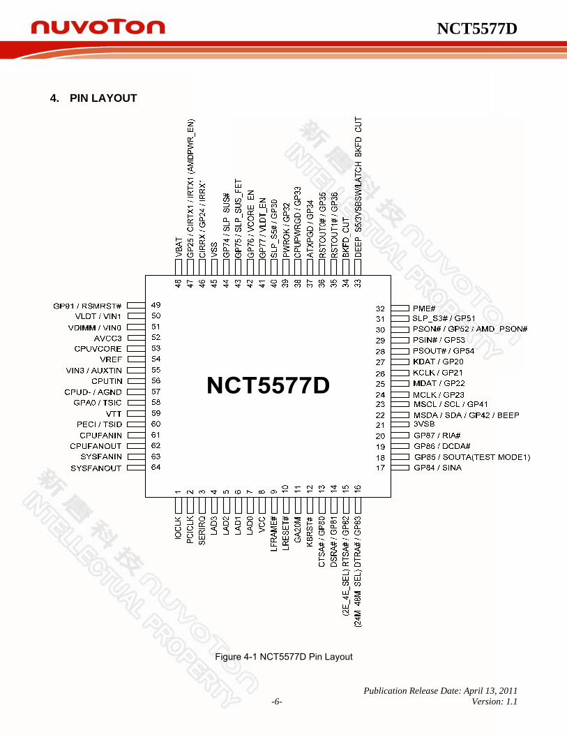
NCT5577D
Publication Release Date: April 13, 2011 -6- Version: 1.1
4. PIN LAYOUT
Figure 4-1 NCT5577D Pin Layout

NCT5577D
Publication Release Date: April 13, 2011 -7- Version: 1.1
5. PIN DESCRIPTION Note: Please refer to 20.2 DC CHARACTERISTICS for details. AOUT - Analog output pin AIN - Analog input pin INtp3 - 3.3V TTL-level input pin INtsp3 - 3.3V TTL-level, Schmitt-trigger input pin INgp5 - 5V GTL-level input pin INtp5 - 5V TTL-level input pin INtscup5 - 5V TTL-level, Schmitt-trigger, input buffer with controllable pull-up INtsp5 - 5V TTL-level, Schmitt-trigger input pin INtdp5 - 5V TTL-level input pin with internal pull-down resistor O8 - output pin with 8-mA source-sink capability OD8 - open-drain output pin with 8-mA sink capability O12 - output pin with 12-mA source-sink capability OD12 - open-drain output pin with 12-mA sink capability O24 - output pin with 24-mA source-sink capability OD24 - open-drain output pin with 24-mA sink capability O48 - output pin with 48-mA source-sink capability OD48 - open-drain output pin with 48-mA sink capability I/Ov3 - Bi-direction pin with source capability of 6 mA and sink capability of 1 mA I/Ov4 - Bi-direction pin with source capability of 6 mA O12cu - output pin 12-mA source-sink capability with controllable pull-up OD12cu - open-drain 12-mA sink capability output pin with controllable pull-up

NCT5577D
Publication Release Date: April 13, 2011 -8- Version: 1.1
5.1 LPC Interface
PIN SYMBOL I/O BUFFER
TYPE POWER WELL DESCRIPTION
1 IOCLK I INtp3 VCC System clock input, either 24MHz or 48MHz. The actual frequency must be specified in the register. The default value is 48MHz.
32 PME# O OD12 VSB Generated PME event.
2 PCICLK I INtsp3 VCC PCI-clock 33-MHz input.
3 SERIRQ I/O I/O12tp3 VCC Serialized IRQ input / output.
4-7 LAD[3:0] I/O I/O12tp3 VCC These signal lines communicate address, control, and data information over the LPC bus between a host and a peripheral.
9 LFRAME# I INtsp3 VCC Indicates the start of a new cycle or the termination of a broken cycle.
10 LRESET# I INtsp3 VCC Reset signal. It can be connected to the PCIRST# signal on the host.
5.2 Serial Port Interface
PIN SYMBOL I/O BUFFER TYPE
POWER WELL DESCRIPTION
20 RIA# I INt VCC Ring Indicator. An active-low signal indicates that a ring signal is being received from the modem or the data set.
19 DCDA# I Int VCC Data Carrier Detection. An active-low signal indicates the modem or data set has detected a data carrier.
18 SOUTA O O8 VCC UART A Serial Output. This pin is used to transmit serial data out to the communication link.
17 SINA I INt VCC Serial Input. This pin is used to receive serial data through the communication link.
16 DTRA# O O8 VCC UART A Data Terminal Ready. An active-low signal informs the modem or data set that the controller is ready to communicate.
15 RTSA# O O8 VCC UART A Request To Send. An active-low signal informs the modem or data set that the controller is ready to send data.
14 DSRA# I INt VCC Data Set Ready. An active-low signal indicates the modem or data set is ready to establish a communication link and transfer data to the UART.
13 CTSA# I INt VCC Clear To Send. This is the modem-control input. The function of these pins can be tested by reading bit 4 of the handshake status register.
5.3 KBC Interface

NCT5577D
Publication Release Date: April 13, 2011 -9- Version: 1.1
PIN SYMBOL I/O BUFFER TYPE
POWER WELL
DESCRIPTION
11 GA20M O O12 VCC Gate A20 output. This pin is high after system reset. (KBC P21)
12 KBRST# O O12 VCC Keyboard reset. This pin is high after system reset. (KBC P20)
26 KCLK I/O INtsp5 OD12
VSB Keyboard Clock.
27 KDAT I/O INtsp5 OD12
VSB Keyboard Data.
24 MCLK I/O INtsp5 OD12
VSB PS2 Mouse Clock.
25 MDAT I/O INtsp5 OD12
VSB PS2 Mouse Data.
5.4 CIR Interface
PIN SYMBOL I/O BUFFER TYPE
POWER WELL
DESCRIPTION
46 CIRRX I INtsp5 VSB CIR input for long length
47 CIRTX1 O O12 VSB CIR transmission output
5.5 Hardware Monitor Interface
PIN SYMBOL I/O BUFFER TYPE
POWER WELL
DESCRIPTION
50 VIN1 I AIN AVCC3 Analog input for voltage measurement (Range: 0 to 2.048 V)
51 VIN0 I AIN AVCC3 Analog input for voltage measurement (Range: 0 to 2.048 V)
53 CPUVCORE I AIN AVCC3 Analog input for voltage measurement (Range: 0 to 2.048 V)
54 VREF O AOUT AVCC3 Reference Voltage (around 2.048 V).
55 VIN3 / AUXTIN I AIN AVCC3 Analog input for voltage measurement (Range: 0 to 2.048V)
56 CPUTIN I AIN AVCC3 The input of temperature sensor 2. It is used for CPU temperature sensing.
61 CPUFANIN I INtsp5 VCC 0 to +5 V amplitude fan tachometer input.
62 CPUFANOUT O O12
OD12 VCC PWM duty-cycle signal for fan speed control.
63 SYSFANIN I INtsp5 VCC 0 to +5 V amplitude fan tachometer input.
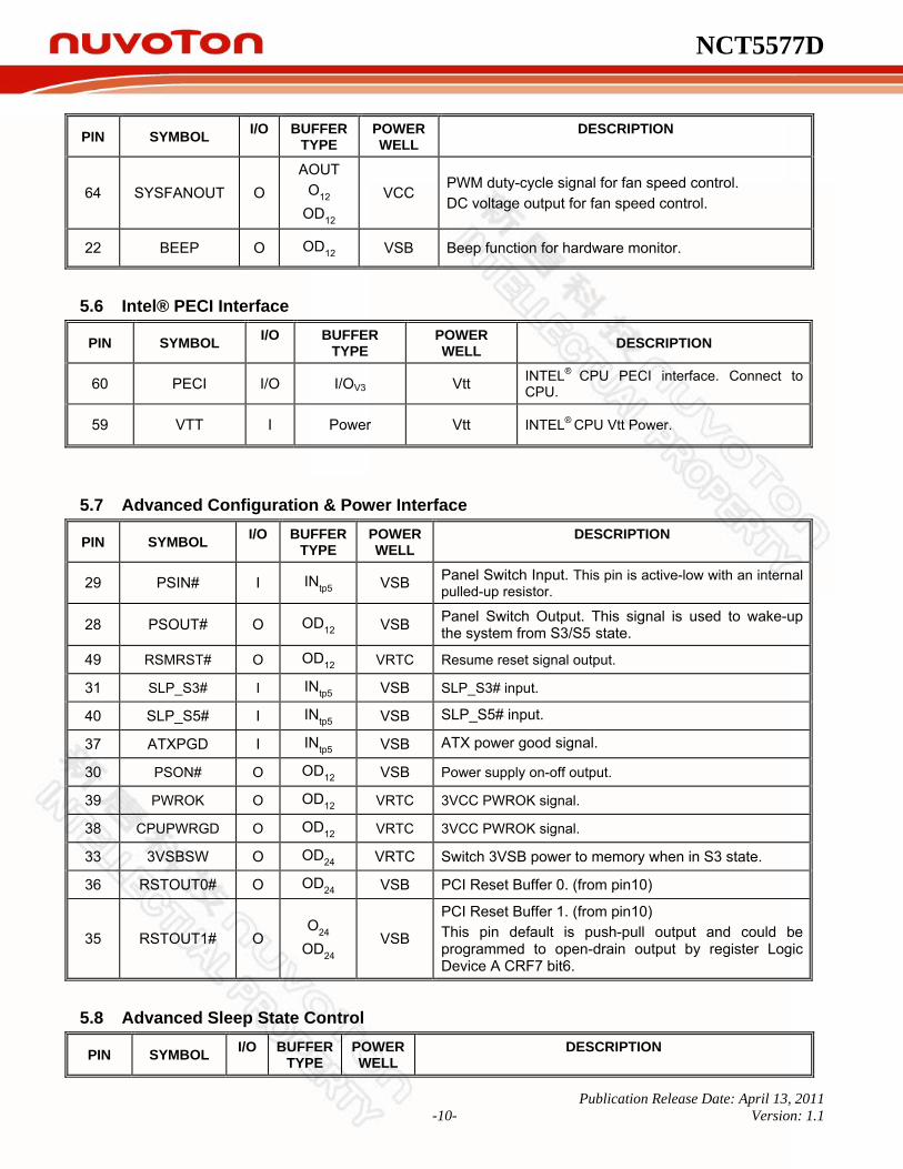
NCT5577D
Publication Release Date: April 13, 2011 -10- Version: 1.1
PIN SYMBOL I/O BUFFER TYPE
POWER WELL
DESCRIPTION
64 SYSFANOUT O AOUT
O12 OD12
VCC PWM duty-cycle signal for fan speed control. DC voltage output for fan speed control.
22 BEEP O OD12 VSB Beep function for hardware monitor.
5.6 Intel® PECI Interface
PIN SYMBOL I/O BUFFER TYPE
POWER WELL DESCRIPTION
60 PECI I/O I/OV3 Vtt INTEL® CPU PECI interface. Connect to
CPU.
59 VTT I Power Vtt INTEL® CPU Vtt Power.
5.7 Advanced Configuration & Power Interface
PIN SYMBOL I/O BUFFER TYPE
POWER WELL
DESCRIPTION
29 PSIN# I INtp5 VSB Panel Switch Input. This pin is active-low with an internal pulled-up resistor.
28 PSOUT# O OD12 VSB Panel Switch Output. This signal is used to wake-up the system from S3/S5 state.
49 RSMRST# O OD12 VRTC Resume reset signal output.
31 SLP_S3# I INtp5 VSB SLP_S3# input.
40 SLP_S5# I INtp5 VSB SLP_S5# input.
37 ATXPGD I INtp5 VSB ATX power good signal.
30 PSON# O OD12 VSB Power supply on-off output.
39 PWROK O OD12 VRTC 3VCC PWROK signal.
38 CPUPWRGD O OD12 VRTC 3VCC PWROK signal.
33 3VSBSW O OD24 VRTC Switch 3VSB power to memory when in S3 state.
36 RSTOUT0# O OD24 VSB PCI Reset Buffer 0. (from pin10)
35 RSTOUT1# O O24
OD24 VSB
PCI Reset Buffer 1. (from pin10) This pin default is push-pull output and could be programmed to open-drain output by register Logic Device A CRF7 bit6.
5.8 Advanced Sleep State Control
PIN SYMBOL I/O BUFFER TYPE
POWER WELL
DESCRIPTION

NCT5577D
Publication Release Date: April 13, 2011 -11- Version: 1.1
PIN SYMBOL I/O BUFFER TYPE
POWER WELL
DESCRIPTION
33 DEEP_S5 O OD24 VSB This pin is to control system power for entering “more power saving mode”.
5.9 SMBus Interface
PIN SYMBOL I/O BUFFER TYPE
POWER WELL DESCRIPTION
23 SCL I/O INtsp5 OD12
VSB SMBus slave clock.
22 SDA I/O INtsp5 OD12
VSB SMBus slave bi-directional Data.
23 MSCL I/O INtsp5 OD12
VSB SMBus master clock.
22 MSDA I/O INtsp5 OD12
VSB SMBus master bi-directional Data.
5.10 Power Pins
PIN SYMBOL I/O BUFFER TYPE
POWER WELL DESCRIPTION
21 3VSB I 3VSB +3.3 V stand-by power supply for the digital circuits.
48 VBAT I VBAT +3 V on-board battery for the digital circuits.
8 VCC I VCC +3.3 V power supply for driving 3 V on host interface.
52 AVCC3 I AVCC3 Analog +3.3 V power input. Internally supply power to all analog circuits.
57 CPUD- / AGND I
CPUD- / AGND
Analog ground. The ground reference for all analog input. Internally connected to all analog circuits. This pin should be connected to ground.
45 VSS I VSS Ground.
5.11 AMD Power-On Sequence
PIN SYMBOL I/O BUFFER TYPE
POWER WELL DESCRIPTION
53 CPUVCORE I AIN AVCC3 Power sequence group B signal
50 VLDT I AIN AVCC3 Power sequence group C signal
51 VDIMM I AIN AVCC3 Memory power enable
42 VCORE_EN O OD12 VSB CPU Vcore power enable
41 VLDT_EN O OD12 VSB Hyper transport I/O power enable
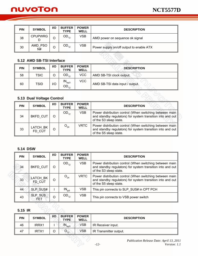
NCT5577D
Publication Release Date: April 13, 2011 -12- Version: 1.1
PIN SYMBOL I/O BUFFER TYPE
POWER WELL DESCRIPTION
38 CPUPWRGD O OD12 VSB AMD power on sequence ok signal
30 AMD_PSON# O OD12 VSB Power supply on/off output to enable ATX
5.12 AMD SB-TSI Interface
PIN SYMBOL I/O BUFFER TYPE
POWER WELL DESCRIPTION
58 TSIC O OD12 VCC AMD SB-TSI clock output.
60 TSID I/O INtsp3 OD12
VCC AMD SB-TSI data input / output.
5.13 Dual Voltage Control
PIN SYMBOL I/O BUFFER TYPE
POWER WELL DESCRIPTION
34 BKFD_CUT O OD12 VSB Power distribution control (When switching between main
and standby regulators) for system transition into and out of the S3 sleep state.
33 LATCH_BKFD_CUT O
O24 VRTC Power distribution control (When switching between main and standby regulators) for system transition into and out of the S5 sleep state.
5.14 DSW
PIN SYMBOL I/O BUFFER TYPE
POWER WELL DESCRIPTION
34 BKFD_CUT O OD12 VSB Power distribution control (When switching between main
and standby regulators) for system transition into and out of the S3 sleep state.
33 LATCH_BKFD_CUT O
O24 VRTC Power distribution control (When switching between main and standby regulators) for system transition into and out of the S5 sleep state.
44 SLP_SUS# I INtp5 VSB This pin connects to SLP_SUS# in CPT PCH
43 SLP_SUS_FET O OD12 VSB This pin connects to VSB power switch
5.15 IR
PIN SYMBOL I/O BUFFER TYPE
POWER WELL DESCRIPTION
46 IRRX1 I INtsp5 VSB IR Receiver input.
47 IRTX1 O O12 VSB IR Transmitter output.

NCT5577D
Publication Release Date: April 13, 2011 -13- Version: 1.1
5.16 General Purpose I/O Port
5.16.1 GPIO-2 Interface
PIN SYMBOL I/O BUFFER TYPE
POWER WELL
DESCRIPTION
27 GP20
I/O INtsp5 O12
OD12 VSB General-purpose I/O port 2 bit 0.
26 GP21
I/O INtsp5 O12
OD12 VSB General-purpose I/O port 2 bit 1.
25 GP22
I/O INtsp5 O12
OD12 VSB General-purpose I/O port 2 bit 2.
24 GP23
I/O INtsp5 O12
OD12 VSB General-purpose I/O port 2 bit 3.
46 GP24
I/O INtsp5 O12
OD12 VSB General-purpose I/O port 2 bit 4.
47 GP25
I/O INtp5 O12
OD12 VSB General-purpose I/O port 2 bit 5.
5.16.2 GPIO-3 Interface
PIN SYMBOL I/O BUFFER TYPE
POWER WELL
DESCRIPTION
40 GP30
I/O INtp5 O12
OD12 VSB General-purpose I/O port 3 bit 0.
39 GP32
I/O INtp5 O12
OD12 VSB General-purpose I/O port 3 bit 2.
38 GP33
I/O INtp5 O12
OD12 VRTC General-purpose I/O port 3 bit 3.
37 GP34
I/O INtp5 O12
OD12 VSB General-purpose I/O port 3 bit 4.

NCT5577D
Publication Release Date: April 13, 2011 -14- Version: 1.1
PIN SYMBOL I/O BUFFER TYPE
POWER WELL
DESCRIPTION
36 GP35
I/O INtp5 O24
OD24 VSB General-purpose I/O port 3 bit 5.
35 GP36
I/O INtp5 O24
OD24 VSB General-purpose I/O port 3 bit 6.
5.16.3 GPIO-4 Interface
PIN SYMBOL I/O BUFFER TYPE
POWER WELL
DESCRIPTION
23 GP41
I/O INtsp5 O12
OD12 VSB General-purpose I/O port 4 bit 1.
22 GP42
I/O INtsp5 O12
OD12 VSB General-purpose I/O port 4 bit 2.
5.16.4 GPIO-5 Interface
PIN SYMBOL I/O BUFFER TYPE
POWER WELL
DESCRIPTION
31 GP51
I/O INtp5 O12
OD12 VSB General-purpose I/O port 5 bit 1.
30 GP52
I/O INtp5 O8
OD8 VSB General-purpose I/O port 5 bit 2.
29 GP53
I/O INtp5 O8
OD8 VSB General-purpose I/O port 5 bit 3.
28 GP54
I/O INtp5 O12
OD12 VSB General-purpose I/O port 5 bit 4.
5.16.5 GPIO-7 Interface
PIN SYMBOL I/O BUFFER TYPE
POWER WELL
DESCRIPTION
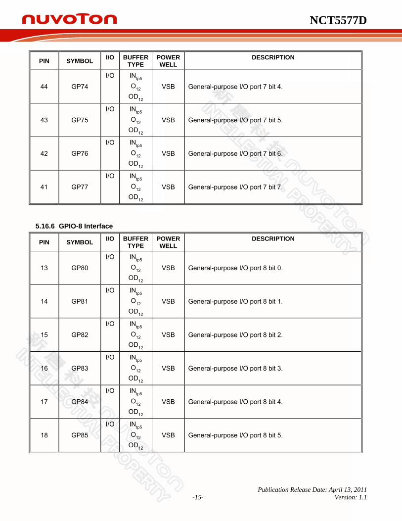
NCT5577D
Publication Release Date: April 13, 2011 -15- Version: 1.1
PIN SYMBOL I/O BUFFER TYPE
POWER WELL
DESCRIPTION
44 GP74
I/O INtp5 O12
OD12 VSB General-purpose I/O port 7 bit 4.
43 GP75
I/O INtp5 O12
OD12 VSB General-purpose I/O port 7 bit 5.
42 GP76
I/O INtp5 O12
OD12 VSB General-purpose I/O port 7 bit 6.
41 GP77
I/O INtp5 O12
OD12 VSB General-purpose I/O port 7 bit 7.
5.16.6 GPIO-8 Interface
PIN SYMBOL I/O BUFFER TYPE
POWER WELL
DESCRIPTION
13 GP80
I/O INtp5 O12
OD12 VSB General-purpose I/O port 8 bit 0.
14 GP81
I/O INtp5 O12
OD12 VSB General-purpose I/O port 8 bit 1.
15 GP82
I/O INtp5 O12
OD12 VSB General-purpose I/O port 8 bit 2.
16 GP83
I/O INtp5 O12
OD12 VSB General-purpose I/O port 8 bit 3.
17 GP84
I/O INtp5 O12
OD12 VSB General-purpose I/O port 8 bit 4.
18 GP85
I/O INtp5 O12
OD12 VSB General-purpose I/O port 8 bit 5.
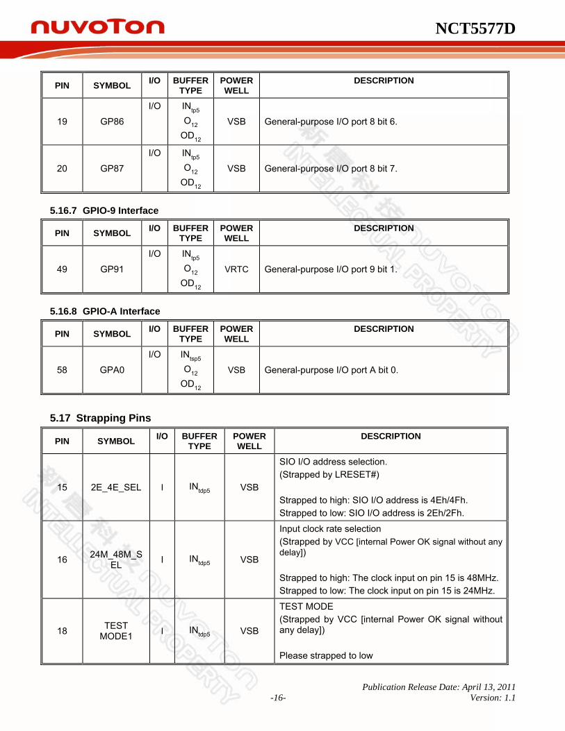
NCT5577D
Publication Release Date: April 13, 2011 -16- Version: 1.1
PIN SYMBOL I/O BUFFER TYPE
POWER WELL
DESCRIPTION
19 GP86
I/O INtp5 O12
OD12 VSB General-purpose I/O port 8 bit 6.
20 GP87
I/O INtp5 O12
OD12 VSB General-purpose I/O port 8 bit 7.
5.16.7 GPIO-9 Interface
PIN SYMBOL I/O BUFFER TYPE
POWER WELL
DESCRIPTION
49 GP91
I/O INtp5 O12
OD12 VRTC General-purpose I/O port 9 bit 1.
5.16.8 GPIO-A Interface
PIN SYMBOL I/O BUFFER TYPE
POWER WELL
DESCRIPTION
58 GPA0
I/O INtsp5 O12
OD12 VSB General-purpose I/O port A bit 0.
5.17 Strapping Pins
PIN SYMBOL I/O BUFFER TYPE
POWER WELL
DESCRIPTION
15 2E_4E_SEL I INtdp5 VSB
SIO I/O address selection. (Strapped by LRESET#) Strapped to high: SIO I/O address is 4Eh/4Fh. Strapped to low: SIO I/O address is 2Eh/2Fh.
16 24M_48M_SEL I INtdp5 VSB
Input clock rate selection (Strapped by VCC [internal Power OK signal without any delay]) Strapped to high: The clock input on pin 15 is 48MHz.Strapped to low: The clock input on pin 15 is 24MHz.
18 TEST MODE1 I INtdp5 VSB
TEST MODE (Strapped by VCC [internal Power OK signal without any delay]) Please strapped to low
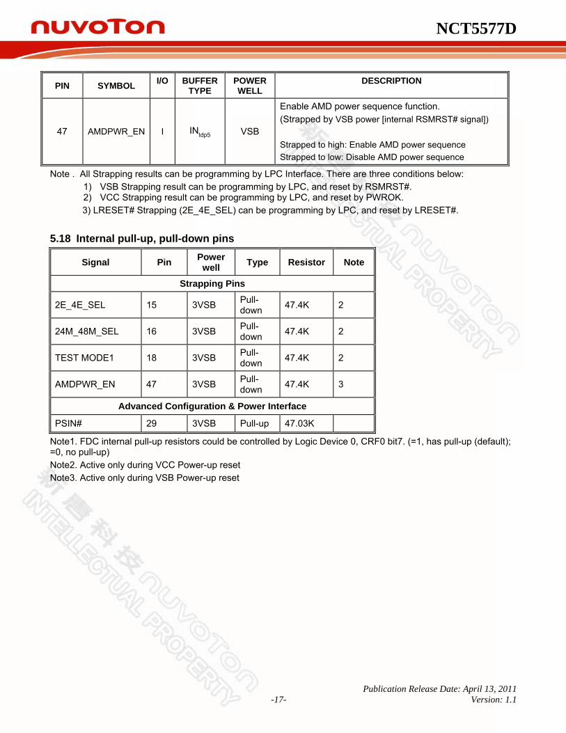
NCT5577D
Publication Release Date: April 13, 2011 -17- Version: 1.1
PIN SYMBOL I/O BUFFER TYPE
POWER WELL
DESCRIPTION
47 AMDPWR_EN I INtdp5 VSB
Enable AMD power sequence function. (Strapped by VSB power [internal RSMRST# signal]) Strapped to high: Enable AMD power sequence Strapped to low: Disable AMD power sequence
Note . All Strapping results can be programming by LPC Interface. There are three conditions below: 1) VSB Strapping result can be programming by LPC, and reset by RSMRST#. 2) VCC Strapping result can be programming by LPC, and reset by PWROK. 3) LRESET# Strapping (2E_4E_SEL) can be programming by LPC, and reset by LRESET#.
5.18 Internal pull-up, pull-down pins
Signal Pin Power well Type Resistor Note
Strapping Pins
2E_4E_SEL 15 3VSB Pull-down 47.4K 2
24M_48M_SEL 16 3VSB Pull-down 47.4K 2
TEST MODE1 18 3VSB Pull-down 47.4K 2
AMDPWR_EN 47 3VSB Pull-down 47.4K 3
Advanced Configuration & Power Interface
PSIN# 29 3VSB Pull-up 47.03K
Note1. FDC internal pull-up resistors could be controlled by Logic Device 0, CRF0 bit7. (=1, has pull-up (default); =0, no pull-up) Note2. Active only during VCC Power-up reset Note3. Active only during VSB Power-up reset
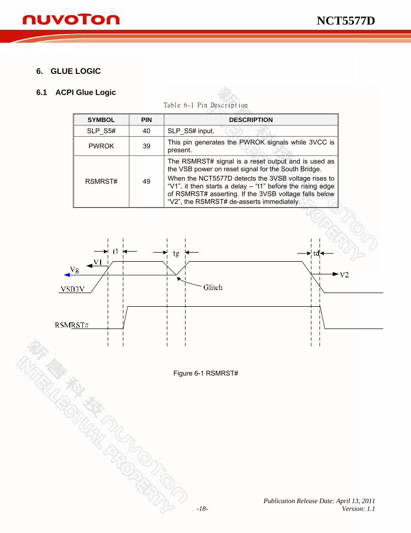
NCT5577D
Publication Release Date: April 13, 2011 -18- Version: 1.1
6. GLUE LOGIC
6.1 ACPI Glue Logic Table 6-1 Pin Description
SYMBOL PIN DESCRIPTION
SLP_S5# 40 SLP_S5# input.
PWROK 39 This pin generates the PWROK signals while 3VCC is present.
RSMRST# 49
The RSMRST# signal is a reset output and is used as the VSB power on reset signal for the South Bridge. When the NCT5577D detects the 3VSB voltage rises to “V1”, it then starts a delay – “t1” before the rising edge of RSMRST# asserting. If the 3VSB voltage falls below “V2”, the RSMRST# de-asserts immediately.
Figure 6-1 RSMRST#

NCT5577D
Publication Release Date: April 13, 2011 -19- Version: 1.1
t2
V3 V4
PWROK
3VCC
Figure 6-2 PWROK
RSTOUTx#
LRESET#
3VCC
t9 t10
Figure 6-3 RSTOUT# and LRESET#
TIMING PARAMETER MIN MAX UNIT
t1 Valid 3VSB to RSMRST# inactive 200 300 mS
t2 Valid 3VCC to PWROK active 300 500 mS
t9 LRESET# active to RSTOUTx# active 0 80 nS
t10 LRESET# inactive to RSTOUTx# inactive 0 80 nS
tg 3VSB Glitch allowance 1 uS
td Falling 3VSB supply Delay 1 uS
DC PARAMETER MIN MAX UNIT V1 3VSB Valid Voltage - 3.033 Volt
V2 3VSB Ineffective Voltage 2.882 - Volt
Vg 3VSB drops by Power noise 2 - Volt
V3 3VCC Valid Voltage - 2.83 Volt
V4 3VCC Ineffective Voltage 2.68 - Volt
Note: 1. The values above are the worst-case results of R&D simulation.
2. About Resume Reset Logic please refer to section 6.3 for more information.

NCT5577D
Publication Release Date: April 13, 2011 -20- Version: 1.1
6.2 BKFD_CUT & LATCH_BKFD_CUT NCT5577D supports BKFD_CUT & LATCH_BKFD_CUT functions, please refer the timing diagram below:
SLP_S5#
SLP_S3#
PWRGD_PS
BKFD_CUT
LATCHED_BF_CUT
TL TL TLTL
TL = 1 us (max)
Figure 6-4 BKFD_CUT and LATCH_BKFD_CUT
BKFD_CUT (Backfeed_Cut) – When high, switches dual rails to standby power.
LATCH_BKFD_CUT (Latched_Backfeed_Cut) – When high, switches dual rails to standby power.
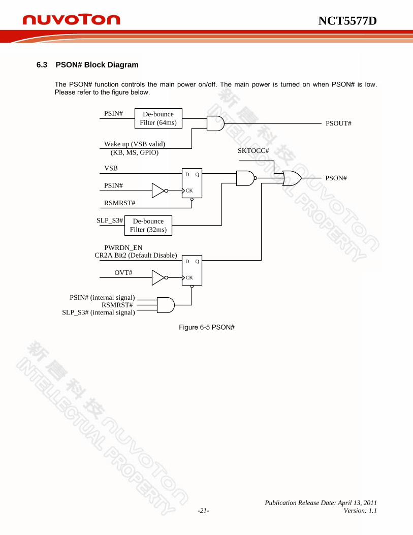
NCT5577D
Publication Release Date: April 13, 2011 -21- Version: 1.1
6.3 PSON# Block Diagram The PSON# function controls the main power on/off. The main power is turned on when PSON# is low. Please refer to the figure below.
D
CK
Q
De-bounceFilter (64ms)
De-bounceFilter (32ms)
D
CK
Q
PSIN#
Wake up (VSB valid)(KB, MS, GPIO)
PSOUT#
VSB
PSIN#
RSMRST#
SLP_S3#
PWRDN_EN
OVT#
PSIN# (internal signal)RSMRST#
SLP_S3# (internal signal)
CR2A Bit2 (Default Disable)
SKTOCC#
PSON#
Figure 6-5 PSON#

NCT5577D
Publication Release Date: April 13, 2011 -22- Version: 1.1
6.4 PWROK PWROK Signal indicates the main power (VCC Power) is valid. Besides, valid PWROK signal also requires the following conditions, as shown in the figure below.
Figure 6-6 PWROK Block Diagram

NCT5577D
Publication Release Date: April 13, 2011 -23- Version: 1.1
6.5 Front Panel LEDs NCT5577D supports two LED control pins – GRN_LED and YLW_LED via GPIO pins. For dual-color LED application:
(1)GRN_LED pin is connected to a 470ohm resistor to 5VSB, and the cathode of the green LED and the anode of the yellow LED. (2)YLW_LED pin is connected to a 470ohm resistor to 5VSB, and the cathode of the yellow LED and the anode of the green LED.
Figure 6-7 Illustration of Dual Color LED application
GRN_LED and YLW_LED pins are designed to show currently power states. There are Manual Mode and Automatic Mode:
6.5.1 Automatic Mode Power state is S0 or S1: GRN_LED will be asserted by default. Power state is S3: YLW_LED will be asserted by default. Power states is S4 or S5: Both GRN_LED and YLW_LED will be de-asserted by default.
AUTO_EN GRN_LED_RST (YLW_LED_RST)
Pwr State SLP_S3# SLP_S5# GRN_LED YLW_LED
1 X S0,S1 1 1 GRN_BLK_FREQ HIGH-Z
1 X S3 0 1 HIGH-Z YLW_BLK_FREQ
1 X S4,S5 X 0 HIGH-Z HIGH-Z

NCT5577D
Publication Release Date: April 13, 2011 -24- Version: 1.1
6.5.2 Manual Mode AUTO_EN GRN_LED_RST# Pwr State SLP_S3# SLP_S5# GRN_LED YLW_LED 0 0 S0,S1 1 1 GRN_BLK_FREQ YLW_BLK_FREQ
0 0 S3 0 1 HIGH-Z HIGH-Z
0 0 S4,S5 X 0 HIGH-Z HIGH-Z
0 1 S0,S1 1 1 GRN_BLK_FREQ YLW_BLK_FREQ
0 1 S3 0 1 GRN_BLK_FREQ YLW_BLK_FREQ
0 1 S4,S5 X 0 GRN_BLK_FREQ YLW_BLK_FREQ
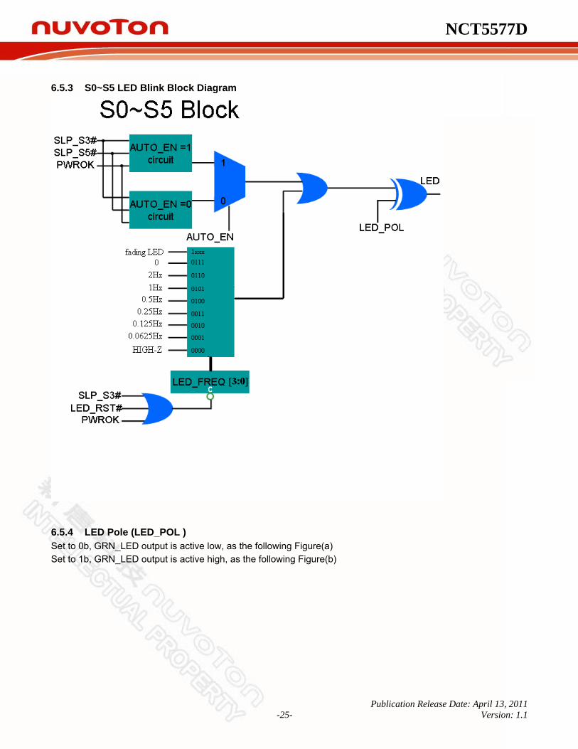
NCT5577D
Publication Release Date: April 13, 2011 -25- Version: 1.1
6.5.3 S0~S5 LED Blink Block Diagram
6.5.4 LED Pole (LED_POL ) Set to 0b, GRN_LED output is active low, as the following Figure(a) Set to 1b, GRN_LED output is active high, as the following Figure(b)

NCT5577D
Publication Release Date: April 13, 2011 -26- Version: 1.1
Figure 6-8 Illustration of LED polarity
6.5.5 Deeper Sleeping State Detect Function These two LED pins could also be used to indicate if the system is in Deeper Sleeping State. For more detail, please refer to the section of Advanced Sleep State Control Function.
Enable_DEEP_S5
GRN_DEEPS#_Disable (YLW_DEEPS#_Disable)
Pwr State
GRN_LED YLW_LED
1 0 DEEP_S5
DeepS5_GRN_BLK_FREQ DeepS5_YLW_BLK_FREQ
1 1 DEEP_S5
HIGH-Z HIGH-Z
0 X S0~S5 S0~S5 behavior S0~S5 behavior
Enable_DEEP_S3
GRN_DEEPS#_Disable (YLW_DEEPS#_Disable)
Pwr State
GRN_LED YLW_LED
1 0 DEEP_S3
DeepS3_GRN_BLK_FREQ DeepS3_YLW_BLK_FREQ
1 1 DEEP_S3
HIGH-Z HIGH-Z
0 X S0~S5 S0~S5 behavior S0~S5 behavior
GRN_LED
VSB or VCC
LED
(a) Active Low
GRN_LED
VSB or VCC
LED
(b) Active High

NCT5577D
Publication Release Date: April 13, 2011 -27- Version: 1.1

NCT5577D
Publication Release Date: April 13, 2011 -28- Version: 1.1
6.6 Advanced Sleep State Control (ASSC) Function Advanced Sleep State Control (ASSC) Function is used to control the system power at S3 or S5 state. The purpose of this function is to provide a method to reduce power consumption at S3 or S5 state. This function is disabled by default. When VCC power is first supplied, BIOS can program the register to enable ASSC Function. The register is powered by 3VSB_IO and some is powered by VBAT. The related registers are located at Logic Device 16 CRE0h ~ CRE3h.
PowerSwitch
ATX Power
Reg
3VSB_IODeep_S5
PSOUT#
SIO
SouthBridgepr
ecis
ion
resi
stor
(1K
)
ACPI Event
PSIN#, KB MS Wakeup,
CIR Wakeup, GPIO Wakeup ACPI Event
3VSB IO Power Domain 3VSB SYS Power Domain
Figure 6-9 ASSC Application Diagram
6.6.1 When ASSC is disabled
When ASSC is disabled, ACPI function is as same as the normal ACPI behavior.
6.6.2 When ASSC is enabled (Enter into Deeper Sleeping State)
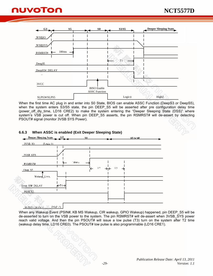
NCT5577D
Publication Release Date: April 13, 2011 -29- Version: 1.1
3VSB_IO
180msRSMRST#
Deep_S5
3VSB_SYS
3VCCBISO Enable
ASSC Function
SLPS3#/SLPS5 HighZLogic 0
T1
G3 S5 S0 S3/S5 Deeper Sleeping State
DeepS5#_DELAY_
When the first time AC plug in and enter into S0 State, BIOS can enable ASSC Function (DeepS3 or DeepS5), when the system enters S3/S5 state, the pin DEEP_S5 will be asserted after pre configuration delay time (power_off_dly_time, LD16 CRE2) to make the system entering the “Deeper Sleeping State (DSS)” where system’s VSB power is cut off. When pin DEEP_S5 asserts, the pin RSMRST# will de-assert by detecting PSOUT# signal (monitor 3VSB SYS Power).
6.6.3 When ASSC is enabled (Exit Deeper Sleeping State)
When any Wakeup Event (PSIN#, KB MS Wakeup, CIR wakeup, GPIO Wakeup) happened, pin DEEP_S5 will be de-asserted to turn on the VSB power to the system. The pin RSMRST# will de-assert when 3VSB_SYS power reach valid voltage. And then the pin PSOUT# will issue a low pulse (T3) turn on the system after T2 time (wakeup delay time, LD16 CRE0). The PSOUT# low pulse is also programmable (LD16 CRE1).

NCT5577D
Publication Release Date: April 13, 2011 -30- Version: 1.1
6.7 Intel DSW Function
6.7.1 Enter DSW State timing diagram

NCT5577D
Publication Release Date: April 13, 2011 -31- Version: 1.1
6.7.2 Exit DSW State timing diagram

NCT5577D
Publication Release Date: April 13, 2011 -32- Version: 1.1
6.8 AMD Power-On Sequence
SIOSB
ATX
PSIN# PSOUT#
PSON#
VCC OFF
AMD power control
SLP_S5#SLP_S3#
We support new AMD power on sequence bace on ACPI power on sequence; therefore, user can choose which architecture by set the strapping pin GP25. If GP52 is 0, only ACPI power on sequence is set; otherwise, AMD power on sequence is combined with ACPI, user can set CR2F[5] to get the same condition. To make sure CR2B[4]:GP34_SEL and CR2B[0]:GP30_SEL are “0” before running the sequence, because they are ATXPGD and SLP_S5# pin select.
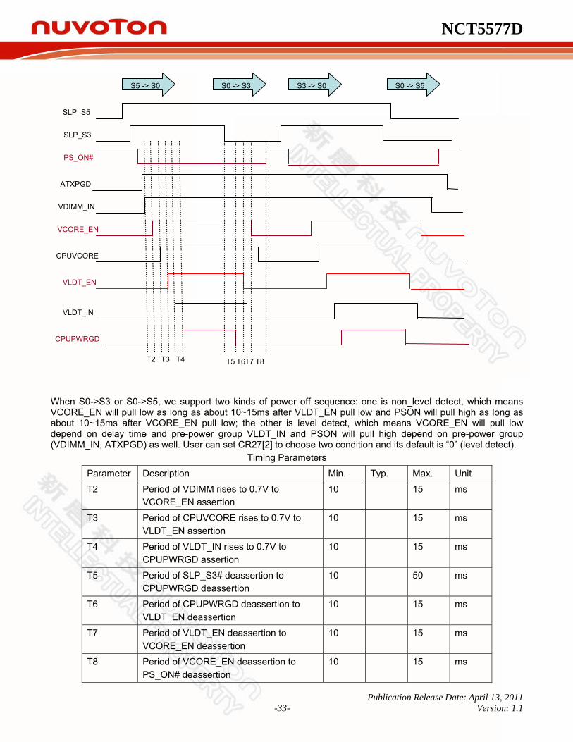
NCT5577D
Publication Release Date: April 13, 2011 -33- Version: 1.1
When S0->S3 or S0->S5, we support two kinds of power off sequence: one is non_level detect, which means VCORE_EN will pull low as long as about 10~15ms after VLDT_EN pull low and PSON will pull high as long as about 10~15ms after VCORE_EN pull low; the other is level detect, which means VCORE_EN will pull low depend on delay time and pre-power group VLDT_IN and PSON will pull high depend on pre-power group (VDIMM_IN, ATXPGD) as well. User can set CR27[2] to choose two condition and its default is “0” (level detect).
Timing Parameters
Parameter Description Min. Typ. Max. Unit
T2 Period of VDIMM rises to 0.7V to VCORE_EN assertion
10 15 ms
T3 Period of CPUVCORE rises to 0.7V to VLDT_EN assertion
10 15 ms
T4 Period of VLDT_IN rises to 0.7V to CPUPWRGD assertion
10 15 ms
T5 Period of SLP_S3# deassertion to CPUPWRGD deassertion
10 50 ms
T6 Period of CPUPWRGD deassertion to VLDT_EN deassertion
10 15 ms
T7 Period of VLDT_EN deassertion to VCORE_EN deassertion
10 15 ms
T8 Period of VCORE_EN deassertion to PS_ON# deassertion
10 15 ms
SLP_S5
SLP_S3
PS_ON#
VDIMM_IN
VCORE_EN
CPUVCORE
VLDT_EN
VLDT_IN
CPUPWRGD
ATXPGD
T2 T3 T4 T5 T6T7 T8
S5 -> S0 S0 -> S3 S3 -> S0 S0 -> S5

NCT5577D
Publication Release Date: April 13, 2011 -34- Version: 1.1
VDDA: 2.5V (not controlled by SIO) VDIMM: DDR 1.8V, DDR3 1.5V (not controlled by SIO) VLDT: 1.2V VCORE: 0.8V ~ 1.55V
To support AMD power on sequence, we add some Pinout as VLDT_EN, VCORE_EN, VLDT_12, VDIMM_18. The sequence follows the figure above. CPU and NB must conform to the SPEC or else the SIO will suspend at the sequence.

NCT5577D
Publication Release Date: April 13, 2011 -35- Version: 1.1
7. CONFIGURATION REGISTER ACCESS PROTOCOL The NCT5577D uses a special protocol to access configuration registers to set up different types of configurations. The NCT5577D has a total of 24 Logical Devices (from Logical Device 0 to Logical Device 17 with the exception of Logical Device 0, 1, 4, C, D, 10, 11, 12, 13, 14 & 15 for backward compatibility) corresponding to thirteen individual functions: UART A (Logical Device 2), IR (Logical Device 3), Keyboard Controller (Logical Device 5), CIR (Logical Device 6), GPIO 7, 8 & 9 (Logical Device 7), WDT1 & GPIO A (Logical Device 8), GPIO 2, 3, 4, 5 & 7 (Logical Device 9), ACPI (Logical Device A), Hardware Monitor & Front Panel LED (Logical Device B), CIRWAKEUP (Logical Device E), GPIO (Logical Device F), Deep Sleep (Logical Device 16) and GPIOA (Logical Device 17). It would require a large address space to access all of the logical device configuration registers if they were mapped into the normal PC address space. The NCT5577D, then, maps all the configuration registers through two I/O addresses (2Eh/2Fh or 4Eh/4Fh) set at power on by the strap pin 2E_4E_SEL. The two I/O addresses act as an index/data pair to read or write data to the Super I/O. One must write an index to the first I/O address which points to the register and read or write to the second address which acts as a data register. An extra level of security is added by only allowing data updates when the Super I/O is in a special mode, called the Extended Function Mode. This mode is entered by two successive writes of 87h data to the first I/O address. This special mode ensures no false data can corrupt the Super I/O configuration during a program runaway. There are a set of global registers located at index 0h – 2Fh, containing information and configuration for the entire chip. The method to access the control registers of the individual logical devices is straightforward. Simply write the desired logical device number into the global register 07h. Subsequent accesses with indexes of 30h or higher are directly to the logical device registers.
One Per Logical Device
Logical Device No.
Logical Device Configuration
Logical Device Control
#0
#F
#2#1
Figure 7-1 Structure of the Configuration Register

NCT5577D
Publication Release Date: April 13, 2011 -36- Version: 1.1
Table 7-1 Devices of I/O Base Address
LOGICAL DEVICE NUMBER
FUNCTION I/O BASE ADDRESS
0 Reserved
1 Reserved
2 UART A 100h ~ FF8h
3 IR 100h ~ FF8h
4 Reserved
5 Keyboard Controller 100h ~ FFFh
6 CIR 100h ~ FF8h
7 GPIO 7, 8 & 9 Reserved
8 WDT1 ,GPIO A Reserved
9 GPIO 2, 3, 4, 5 &7 Reserved
A ACPI Reserved
B Hardware Monitor & Front Panel LED
100h ~ FFEh
C Reserved
D Reserved
E CIRWAKEUP 100h ~ FF8h
F GPIO Reserved
10 Reserved
11 Reserved
12 Reserved
13 Reserved
14 Reserved
15 Reserved
16 Deep Sleep Reserved
17 GPIO A Reserved

NCT5577D
Publication Release Date: April 13, 2011 -37- Version: 1.1
7.1 Configuration Sequence
Power-on Reset
Wait for key string
Check Pass Key
Extended Function Mode
Is the data “87h”?
Is the data “87h”?
N
N
I/O Write to 2Eh
I/O Write to 2Eh
Any other I/O transition cycle
Any other I/O transition cycle
Figure 7-2 Configuration Register
To program the NCT5577D configuration registers, the following configuration procedures must be followed in sequence: (1). Enter the Extended Function Mode. (2). Configure the configuration registers. (3). Exit the Extended Function Mode.
7.1.1 Enter the Extended Function Mode To place the chip into the Extended Function Mode, two successive writes of 0x87 must be applied to Extended Function Enable Registers (EFERs, i.e. 2Eh or 4Eh).
7.1.2 Configure the Configuration Registers The chip selects the Logical Device and activates the desired Logical Devices through Extended Function Index Register (EFIR) and Extended Function Data Register (EFDR). The EFIR is located at the same address as the EFER, and the EFDR is located at address (EFIR+1). First, write the Logical Device Number (i.e. 0x07) to the EFIR and then write the number of the desired Logical Device to the EFDR. If accessing the Chip (Global) Control Registers, this step is not required.

NCT5577D
Publication Release Date: April 13, 2011 -38- Version: 1.1
Secondly, write the address of the desired configuration register within the Logical Device to the EFIR and then write (or read) the desired configuration register through the EFDR.
7.1.3 Exit the Extended Function Mode To exit the Extended Function Mode, writing 0xAA to the EFER is required. Once the chip exits the Extended Function Mode, it is in the normal running mode and is ready to enter the configuration mode.
7.1.4 Software Programming Example The following example is written in Intel 8086 assembly language. It assumes that the EFER is located at 2Eh, so the EFIR is located at 2Eh and the EFDR is located at 2Fh. If the HEFRAS (CR[26h] bit 6 showing the value of the strap pin at power on) is set, 2Eh can be directly replaced by 4Eh and 2Fh replaced by 4Fh. This example programs the configuration register F0h (clock source) of logical device 1 (UART A) to the value of 3Ch (24MHz). First, one must enter the Extended Function Mode, then setting the Logical Device Number (Index 07h) to 01h. Then program index F0h to 3Ch. Finally, exit the Extended Function Mode. ;----------------------------------------------------- ; Enter the Extended Function Mode ;----------------------------------------------------- MOV DX, 2EH MOV AL, 87H OUT DX, AL OUT DX, AL ;----------------------------------------------------------------------------- ; Configure Logical Device 1, Configuration Register CRF0 ;----------------------------------------------------------------------------- MOV DX, 2EH MOV AL, 07H OUT DX, AL ; point to Logical Device Number Reg. MOV DX, 2FH MOV AL, 01H OUT DX, AL ; select Logical Device 1 ; MOV DX, 2EH MOV AL, F0H OUT DX, AL ; select CRF0 MOV DX, 2FH MOV AL, 3CH OUT DX, AL ; update CRF0 with value 3CH ;----------------------------------------------- ; Exit the Extended Function Mode ;---------------------------------------------- MOV DX, 2EH MOV AL, AAH OUT DX, AL
NCT5577D
Publication Release Date: April 13, 2011 -39- Version: 1.1
8. HARDWARE MONITOR
8.1 General Description The NCT5577D monitors several critical parameters in PC hardware, including power supply voltages, fan speeds, and temperatures, all of which are very important for a high-end computer system to work stably and properly. In addition, proprietary hardware reduces the amount of programming and processor intervention to control cooling fan speeds, minimizing ambient noise and maximizing system temperature and reliability. The NCT5577D can simultaneously monitor all of the following inputs:
• Eight analog voltage inputs (Four internal voltages VBAT, 3VSB, 3VCC and AVCC; four external voltage inputs)
• Two fan tachometer inputs • Two remote temperatures, using either a thermistor or from the CPU thermal diode (voltage or Current
Mode measurement method) These inputs are converted to digital values using the integrated, eight-bit analog-to-digital converter (ADC). In response to these inputs, the NCT5577D can generate the following outputs:
• Two PWM (pulse width modulation) or DC fan outputs for the fan speed control • SMI#
The NCT5577D provides hardware access to all monitored parameters through the LPC or I2C interface and software access through application software, such as Nuvoton’s Health Manager, or BIOS. The rest of this section introduces the various features of the NCT5577D hardware-monitor capability. These features are divided into the following sections:
• Access Interfaces • Analog Inputs • Fan Speed Measurement and Control • Smart Fan Control • SMI# interrupt mode • Registers and Value RAM
8.2 Access Interfaces The NCT5577D provides two interfaces, LPC and I2C, for the microprocessor to read or write the internal registers of the hardware monitor.
8.3 LPC Interface The internal registers of the hardware monitor block are accessible through two separate methods on the LPC bus. The first set of registers, which primarily enable the block and set its address in the CPU I/O address space are accessed by the Super I/O protocol described in Chapter 7 at address 2Eh/2Fh or 4Eh/4Fh. The bulk of the functionality and internal registers of this block are accessed form an index/data pair of CPU I/O addresses. The standard locations are usually 295h/296h and are set by CR [60h] & CR [61h] accessed using the Super I/O protocol as described in Chapter 7.

NCT5577D
Publication Release Date: April 13, 2011 -40- Version: 1.1
Due to the number of internal register, it is necessary to separate the register sets into “banks” specified by register 4Eh. The structure of the internal registers is shown in the following figure.
Configuration Register40h
Interrupt Status Registers41h, 42h
SMI# Mask Registers 43h, 44h, 46h
Fan Divisor Register I47h
4Bh
SMI#/OVT# Control Register4Ch
Fan IN /OUT Control Register4Dh
Bank Select for 50h~5Fh Registers.
4Eh
Winbond Vendor ID4Fh
BANK 0BEEP Control Registers
56h~57h
BANK 0Chip ID Register
58h
BANK 0Temperature Sensor TypeConfiguration & Fan Divisor Registers
59h,5Dh
DataRegister
Port 6h
Port 5h
Index Register
LPCBus
Smart Fan Configuration Registers
00h-1Fh
BANK 4Interrupt Status & SMI# Mask Registers
50h~51h
BANK 4Beep Control Registers
53h
BANK 4Temperature Offset Registers
54h~56h
BANK 4Read Time Status Registers
59h~5Bh
BANK 5
50h~5ChMonitor Value Registers
Fan Divisor Register II
BANK 1CPUTIN TemperatureControl/Stauts Registers
50h~56h
BANK 2 AUXTIN Temperature Control/Stauts Registers
50h~56h
Serial Bus Address48h
FANOUTs Source Select Register
49h, 4Ah
Monitor Value Registers20h~3Fh
BANK 0Cirtical Tempature andCurren mode enable
5Eh
BANK 0Smart Fan Configuration Registers
60h~6Ah
BANK 0FANOUT Critical Temperature
6Bh~6Eh
Figure 8-1 LPC Bus’ Reads from / Write to Internal Registers

NCT5577D
Publication Release Date: April 13, 2011 -41- Version: 1.1
8.4 I2C interface The I2C interface is a second, serial port into the internal registers of the hardware monitor function block. The interface is totally compatible with the industry-standard I2C specification, allowing external components that are also compatible to read the internal registers of the NCT5577D hardware monitor and control fan speeds. The address of the I2C peripheral is set by the register located at index 48h (which is accessed by the index/data pair at I/O address typically at 295h/296h) The two timing diagrams below illustrate how to use the I2C interface to write to an internal register and how to read the value in an internal register, respectively. (a) Serial bus write to internal address register followed by the data byte
0
Start ByMaster
0 1 0 1 1 0 1 D7 D6 D5 D4 D3 D2 D1 D0Ackby
627DHG
R/W
Ackby
627DHG
SCL
SDA
D7 D6 D5 D4 D3 D2 D1 D0Ackby
784R
Stopby
Master
SCL
SDA (Continued)
7 8 0 7 8
07 8
Frame 2Internal Index Register Byte
(Continued)
Frame 3Data Byte
Frame 1Serial Bus Address Byte
Ackby
627DHG
Figure 8-2 Serial Bus Write to Internal Address Register Followed by the Data Byte
(b) Serial bus read from a register
0
D7 D6 D5 D4 D3 D2 D1 D0Ackby
MasterAckby
627DHG
7 8 0 7 8
0
Frame 4Data Byte
Frame 3Serial Bus Address Byte
Stop byMaster
0
Start ByMaster
0 1 0 1 1 0 1 D7 D6 D5 D4 D3 D2 D1 D0R/W
Ackby
627DHG
SCL
SDA
7 8 0 7 8
0
Frame 2Internal Index Register Byte
Frame 1Serial Bus Address Byte
Ackby
627DHG
0 1 0 1 1 0 1 R/W
RepeatstartbyMaster
Figure 8-3 Serial Bus Read from Internal Address Register
8.5
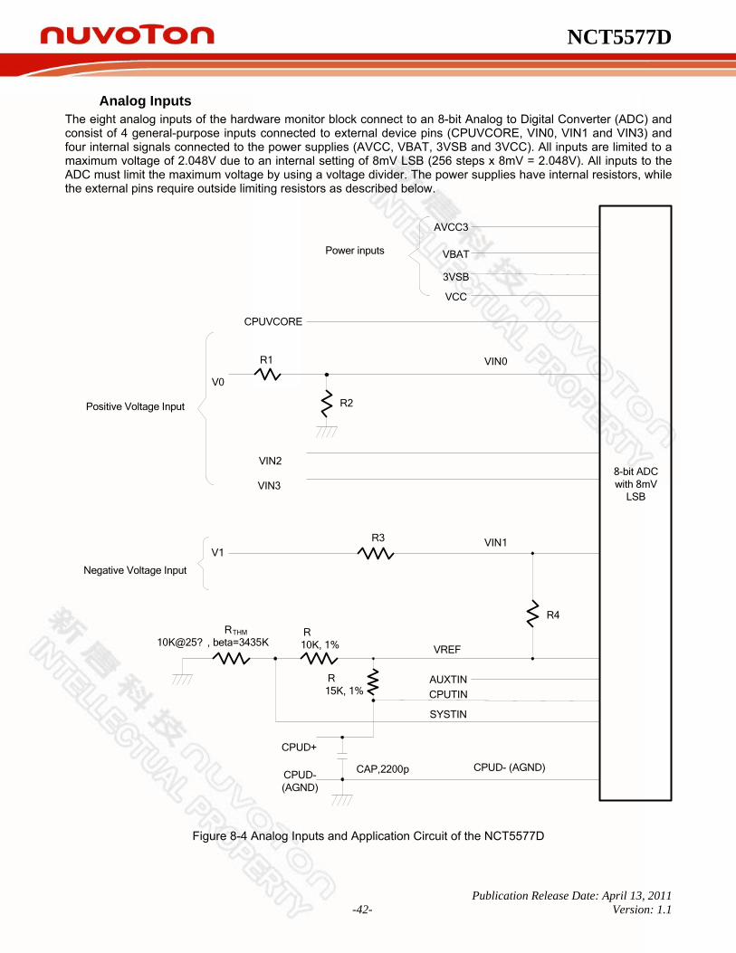
NCT5577D
Publication Release Date: April 13, 2011 -42- Version: 1.1
Analog Inputs The eight analog inputs of the hardware monitor block connect to an 8-bit Analog to Digital Converter (ADC) and consist of 4 general-purpose inputs connected to external device pins (CPUVCORE, VIN0, VIN1 and VIN3) and four internal signals connected to the power supplies (AVCC, VBAT, 3VSB and 3VCC). All inputs are limited to a maximum voltage of 2.048V due to an internal setting of 8mV LSB (256 steps x 8mV = 2.048V). All inputs to the ADC must limit the maximum voltage by using a voltage divider. The power supplies have internal resistors, while the external pins require outside limiting resistors as described below.
VIN2
CPUVCORE
VIN0
VIN1
VBAT
R4
V0
Positive Voltage Input
Negative Voltage Input
VREF
AUXTINCPUTIN
SYSTIN
3VSB
R3
RTHM
10K@25? , beta=3435K
R2
R10K, 1%
V1
AVCC3
CAP,2200p
CPUD+
CPUD-(AGND)
VCC
VIN3
CPUD- (AGND)
Power inputs
8-bit ADC with 8mV
LSB
R1
R15K, 1%
Figure 8-4 Analog Inputs and Application Circuit of the NCT5577D

NCT5577D
Publication Release Date: April 13, 2011 -43- Version: 1.1
As illustrated in the figure above, other connections may require some external circuits. The rest of this section provides more information about voltages outside the range of the 8-bit ADC, CPU Vcore voltage detection, and temperature sensing.
8.5.1 Voltages Over 2.048 V or Less Than 0 V Input voltages greater than 2.048 V should be reduced by an external resistor divider to keep the input voltages in the proper range. For example, input voltage V0 (+12 V) should be reduced before it is connected to VIN0 according to the following equation:
21
200
RRRVVIN+
×=
R1 and R2 can be set to 56 KΩ and 10 KΩ, respectively, to reduce V0 from +12 V to less than 2.048 V. All the internal inputs of the ADC, AVCC, VBAT, 3VSB and 3VCC utilize an integrated voltage divider with both resistors equal to 34KΩ, yielding a voltage one half of the power supply. Since one would expect a worst-case 10% variation or a 3.63V maximum voltage, the input to the ADC will be 1.815V, well within the maximum range.
VKK
KVCCVin 65.13434
34≅
Ω+ΩΩ
×= , where VCC is set to 3.3V
The CPUVCORE pin feeds directly into the ADC with no voltage divider since the nominal voltage on this pin is only 1.2V. Negative voltages are handled similarly, though the equation looks a little more complicated. For example, negative voltage V1 (-12V) can be reduced according to the following equation:
12,048.2)048.2(1 143
41 −=+
+×−= whereV
RRRVVIN
R3 and R4 can be set to 232 KΩ and 10 KΩ, respectively, to reduce negative input voltage V1 from –12 V to less than 2.048 V. Note that R4 is referenced to VREF, or 2.048V instead of 0V to allow for more dynamic range. This is simply good analog practice to yield the most precise measurements. Both of these solutions are illustrated in the figure above.
8.5.2 Voltage Data Format The data format for voltage detection is an eight-bit value, and each unit represents an interval of 8 mV.
Detected Voltage = Reading * 0.008 V If the source voltage was reduced by a voltage divider, the detected voltage value must be scaled accordingly.
NCT5577D has 8 voltage reading:
3VCC AVCC 3VSB VBAT
Voltage reading
Bank0, index23
Bank0, index22
Bank5, Index50
Bank5, Index51
CPUVCORE VIN0 VIN1 VIN3 Voltage reading
Bank0, index20
Bank0, index21
Bank0, index24
Bank0, index26

NCT5577D
Publication Release Date: April 13, 2011 -44- Version: 1.1
8.5.3 Temperature Data Format The data format for sensors CPUTIN and AUXTIN is 9-bit, two’s-complement. This is illustrated in the table below. There are two sources of temperature data: external thermistors or thermal diodes.
Table 8-1 Temperature Data Format
8-BIT DIGITAL OUTPUT 9-BIT DIGITAL OUTPUT TEMPERATURE
8-BIT BINARY 8-BIT HEX 9-BIT BINARY 9-BIT HEX
+125°C 0111,1101 7Dh 0,1111,1010 0FAh
+25°C 0001,1001 19h 0,0011,0010 032h
+1°C 0000,0001 01h 0,0000,0010 002h
+0.5°C - - 0,0000,0001 001h
+0°C 0000,0000 00h 0,0000,0000 000h
-0.5°C - - 1,1111,1111 1FFh
-1°C 1111,1111 FFh 1,1111,1110 1FFh
-25°C 1110,0111 E7h 1,1100,1110 1Ceh
-55°C 1100,1001 C9h 1,1001,0010 192h
8.5.3.1. Monitor Temperature from Thermistor External thermistors should have a β value of 3435K and a resistance of 10 KΩ at 25°C. As illustrated in the schematic above, the thermistor is connected in series with a 10-KΩ resistor and then connects to VREF (pin 54). The configuration registers to select a thermistor temperature sensor and the measurement method are found at Bank 0, index 59h, 5Dh, and 5Eh.
RTHM
10K@25°C, beta = 3435K
R10K, 1%
VREF
AUXTIN
SYSTIN
CPUTIN
Figure 8-5 Monitoring Temperature from Thermistor
8.5.3.2. Monitor Temperature from Thermal Diode (Voltage Mode) The thermal diode D- pin is connected to AGND (pin 57), and the D+ pin is connected to the temperature sensor pin in the NCT5577D. A 15-KΩ resistor is connected to VREF to supply the bias current for the diode, and the 2200-pF, bypass capacitor is added to filter high-frequency noise. The configuration registers to select a thermal diode temperature sensor and the measurement method are found at Bank 0, index 59h, 5Dh, and 5Eh.

NCT5577D
Publication Release Date: April 13, 2011 -45- Version: 1.1
D+
D-
TherminalDiode
C=2200pF
R=15K,1%
VREF
CPUTIN
CPUD-(AGND)
AGND
(SYSTIN)
(AUXTIN)
D+
D-
TherminalDiode
C=2200pF
R=15K,1%
VREF
CPUTIN
CPUD-(AGND)
AGND
(SYSTIN)
(AUXTIN)
Figure 8-6 Monitoring Temperature from Thermal Diode (Voltage Mode)
8.5.3.3. Monitor Temperature from Thermal Diode (Current Mode) The NCT5577D can also sense the diode temperature through Current Mode and the circuit is shown in the following figure.
D+
D-
TherminalDiode
C=2200pF
R=15K,1%
VREF
CPUTIN
CPUD-(AGND)
AGND
(SYSTIN)
(AUXTIN)
D+
D-
TherminalDiode
C=2200pF
R=15K,1%
VREF
CPUTIN
CPUD-(AGND)
AGND
(SYSTIN)
(AUXTIN)
Figure 8-7 Monitoring Temperature from Thermal Diode (Current Mode)
The pin of processor D- is connected to CPUD- (pin 57) and the pin D+ is connected to temperature sensor pin in the NCT5577D. A bypass capacitor C=2200pF should be added to filter the high frequency noise. The configuration registers to select a thermal diode temperature sensor and the measurement method are found at Bank 0, index 59h, 5Dh, and 5Eh.

NCT5577D
Publication Release Date: April 13, 2011 -46- Version: 1.1
8.5.3.4. Temperature Reading NCT5577D has 6 temperature reading can monitor different temperature sources (ex: CPUTIN, AUXTIN, PECI…etc).
SMIOVT1 SMIOVT2 SMIOVT3 SMIOVT4 SMIOVT5 SMIOVT6 Temperature source select
Bank6, index21 bit[4:0] default: SYSTIN
Bank6, index22 bit[4:0] default: CPUTIN
Bank6, index23 bit[4:0] default: AUXTIN
Bank6, index24 bit[4:0] default: SYSTIN
Bank6, index25 bit[4:0] default: SYSTIN
Bank6, index26 bit[4:0] default: SYSTIN
Temperature reading (2’s complement)
Bank0, index27
Bank1, index50 & index51 bit7
Bank2, index50 & index51 bit7
Bank6, index2B & index2E bit0
Bank6, index2C & index2E bit1
Bank6, index2D & index2E bit2
Note. If the temperature source is selecting to PECI, please set Bank0 Index AEh first for reading correct value
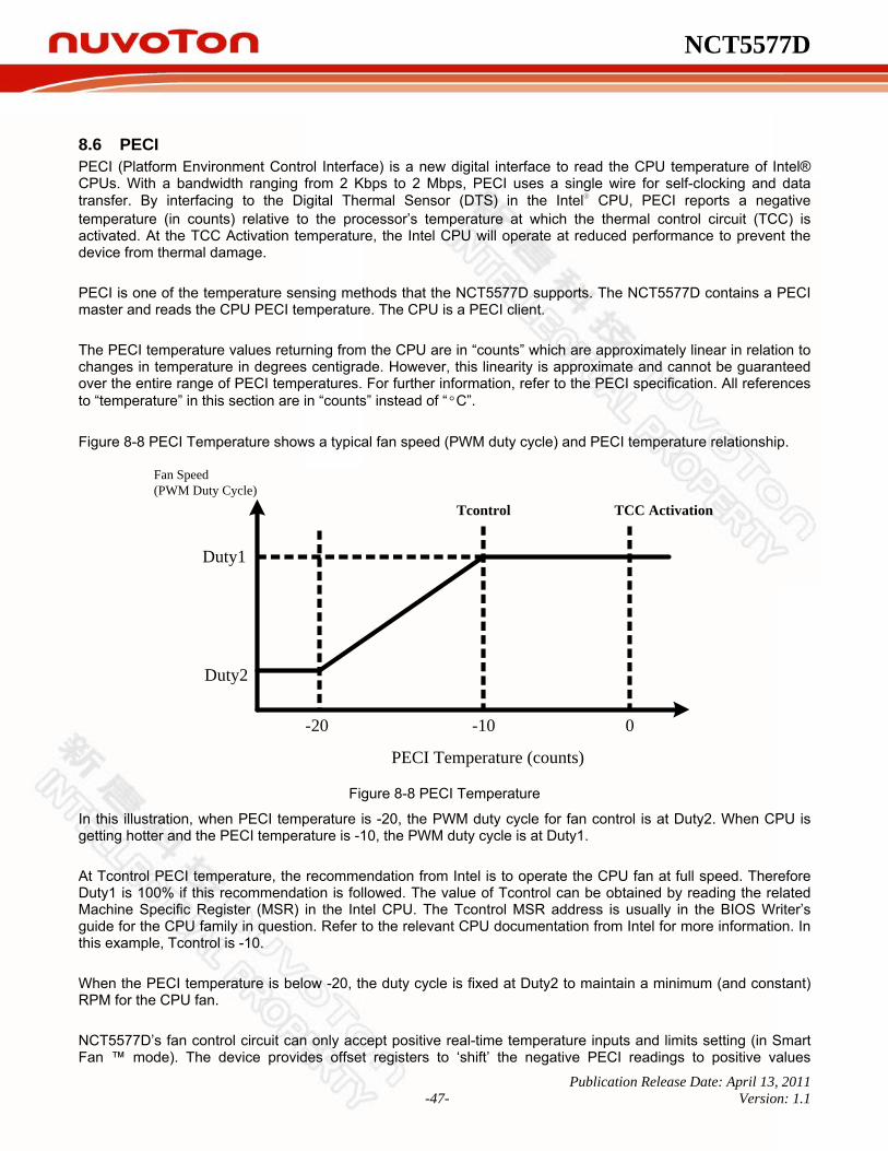
NCT5577D
Publication Release Date: April 13, 2011 -47- Version: 1.1
8.6 PECI PECI (Platform Environment Control Interface) is a new digital interface to read the CPU temperature of Intel® CPUs. With a bandwidth ranging from 2 Kbps to 2 Mbps, PECI uses a single wire for self-clocking and data transfer. By interfacing to the Digital Thermal Sensor (DTS) in the Intel® CPU, PECI reports a negative temperature (in counts) relative to the processor’s temperature at which the thermal control circuit (TCC) is activated. At the TCC Activation temperature, the Intel CPU will operate at reduced performance to prevent the device from thermal damage. PECI is one of the temperature sensing methods that the NCT5577D supports. The NCT5577D contains a PECI master and reads the CPU PECI temperature. The CPU is a PECI client. The PECI temperature values returning from the CPU are in “counts” which are approximately linear in relation to changes in temperature in degrees centigrade. However, this linearity is approximate and cannot be guaranteed over the entire range of PECI temperatures. For further information, refer to the PECI specification. All references to “temperature” in this section are in “counts” instead of “°C”. Figure 8-8 PECI Temperature shows a typical fan speed (PWM duty cycle) and PECI temperature relationship.
Tcontrol TCC Activation
Duty1
Duty2
-20 0-10
PECI Temperature (counts)
Fan Speed(PWM Duty Cycle)
Figure 8-8 PECI Temperature
In this illustration, when PECI temperature is -20, the PWM duty cycle for fan control is at Duty2. When CPU is getting hotter and the PECI temperature is -10, the PWM duty cycle is at Duty1. At Tcontrol PECI temperature, the recommendation from Intel is to operate the CPU fan at full speed. Therefore Duty1 is 100% if this recommendation is followed. The value of Tcontrol can be obtained by reading the related Machine Specific Register (MSR) in the Intel CPU. The Tcontrol MSR address is usually in the BIOS Writer’s guide for the CPU family in question. Refer to the relevant CPU documentation from Intel for more information. In this example, Tcontrol is -10. When the PECI temperature is below -20, the duty cycle is fixed at Duty2 to maintain a minimum (and constant) RPM for the CPU fan. NCT5577D’s fan control circuit can only accept positive real-time temperature inputs and limits setting (in Smart Fan ™ mode). The device provides offset registers to ‘shift’ the negative PECI readings to positive values

NCT5577D
Publication Release Date: April 13, 2011 -48- Version: 1.1
otherwise the fan control circuit will not function properly. The offset registers are the Tbase registers located at Bank7, Index09h for PECI_BASE0; Bank7, Index0Ah for PECI_BASE1; separately. All default values of these Tbase registers are 8’h00.These registers should be programmed with (positive) values so that the resultant value (Tbase + PECI) is always positive. The unit of the Tbase register contents is “count” to match that of PECI values. The resultant value (Tbase + PECI) should not be interpreted as the “temperature” (whether in count or °C) of the PECI client (CPU). Figure 8-9 Temperature and Fan Speed Relation after Tbase Offsetsshows the temperature/fan speed relationship after Tbase offsets are applied (based on Figure 8-8 PECI Temperature). This view is from the perspective of the NCT5577D fan control circuit.
Tcontrol TCC Activation
Duty1
Duty2
90 = (-10 + 100)(PECI = -10)
Temperature (as seen by the W83677HG-I fan control circuit)
(PECI = 0)80 = (-20 + 100)(PECI = -20)
85 = (-15 + 100)(PECI = -15)
Fan Speed(PWM Duty Cycle) Tbase = 100
Figure 8-9 Temperature and Fan Speed Relation after Tbase Offsets
Assuming Tbase is set to 100 and the PECI temperature is -15 , the real-time temperature value to the fan control circuit will be 85 (-15 + 100). The value of 55 (hex) will appear in the relevant real-time temperature register. While using Smart Fan control function of NCT5577D, BIOS/software must include Tbase in determining the thresholds (limits). In this example, assuming Tcontrol is -10 and Tbase is set to 100 (1), the threshold temperature value corresponding to the “100% fan duty cycle” event is 90 (-10+100). The value of 5A (hex) should be written to the relevant threshold register. Tcontrol is typically -10 to -20 for PECI-enabled CPUs. Base on that, a value of 85 ~100 for Tbase could be set for proper operation of the fan control circuit. This recommendation is applicable for most designs. In general, the concept presented in this section could be used to determine the optimum value of Tcontrol to match the specific application.

NCT5577D
Publication Release Date: April 13, 2011 -49- Version: 1.1
8.7 Fan Speed Measurement and Control This section is divided into two parts, one to measure the speed and one to control the speed.
8.7.1 Fan Speed Reading The fan speed reading at:
FAN COUNT READING FAN RPM READING 16-bit 16-bit
[12:5] [4:0] [15:8] [7:0] SYSFANIN Bank6,
index30 Bank6, index31
Bank6, index56
Bank6, index57
CPUFANIN Bank6, index32
Bank6, index33
Bank6, index58
Bank6, index59
8.7.2 Fan Speed Calculation by Fan Count Reading In 16-bit fan count reading, please read high byte first then low byte. Fan speed RPM can be evaluated by the following equation, fan count could be 8-bit or 16-bit:
CountRPM
61035.1 ×=
8.7.3 Fan Speed Calculation by Fan RPM Reading In 16-bit fan RPM reading, please read high byte first then low byte. Fan speed RPM can be evaluated by translating 16-bit RPM reading from hexadecimal to decimal.
Register reading 0x09C4h = 2500 RPM
8.7.4 Fan Speed Control The NCT5577D has two output pins for fan control, each of which offers PWM duty cycle and DC voltage to control the fan speed. The output type (PWM or DC) of each pin is configured by Bank0 index 04h, bits 0 for SYSFANOUT and bits 1 for CPUFANOUT.
SYSFANOUT CPUFANOUT Output Type Select Bank0,
index04 bit0 0: PWM output 1: DC output (default)
Bank0, index04 bit1 0: PWM output (default) 1: DC output
Output Type Select (in PWM output)
CR24 bit4 0: open-drain (default) 1: push-pull
CR24 bit3 0: open-drain (default) 1: push-pull
PWM Output Freqency
Bank0, Index00
Bank0, Index02
Fan Control Mode Bank1, Bank2,

NCT5577D
Publication Release Date: April 13, 2011 -50- Version: 1.1
`64
ValueRegister bit -6 Programmed×=Vref
Select index02, bit[7:4] 0h: Manual mode (def.)1h: Thermal Cruise 2h: Speed Cruise 4h: SMART FAN IV
index02, bit[7:4] 0h: Manual mode(def.) 1h: Thermal Cruise 2h: Speed Cruise 4h: SMART FAN IV
PWM output (Duty)
Bank1, index09 bit[7:0]
Bank2, index09 bit[7:0]
Output Value (write)
DC output (Voltage)
Bank1, index09 bit[7:2]
Bank2, index09 bit[7:2]
Current Output Value (read)
Bank0, index01
Bank0, index03
For PWM, the duty cycle is programmed by eight-bit registers at Bank1 Index 09h for SYSFANOUT and Bank2 Index 09h for CPUFANOUT. The duty cycle can be calculated using the following equation:
%100255
ValueRegister bit -8 Programmed(%)Dutycycle ×=
The default duty cycle is FFh, or 100%. The PWM clock frequency is programmed at Bank0 Index 00h, Index 02h, and Index 10h. For DC, the NCT5577D has a six bit digital-to-analog converter (DAC) that produces 0 to 2.048 Volts DC. The analog output is programmed at Bank1 Index 09h bit[7:2] for SYSFANOUT and Bank2 Index 09h bit[7:2] for CPUFANOUT. The analog output can be calculated using the following equation: OUTPUT Voltage (V) The default value is 111111YY, or nearly 2.048 V, and Y is a reserved bit.
8.7.5 SMART FANTM Control The NCT5577D supports various different fan control features:
SMART FANTM I (Thermal Cruise & Speed Cruise) SMART FANTM IV Close-Loop Fan Control RPM mode
SYSFANOUT CPUFANOUT Fan Control Mode Select
Bank1, index02, bit[7:4] 0h: Manual mode (def.)1h: Thermal Cruise 2h: Speed Cruise 4h: SMART FAN IV
Bank2, index02, bit[7:4] 0h: Manual mode(def.) 1h: Thermal Cruise 2h: Speed Cruise 4h: SMART FAN IV
8.7.6 Temperature Source & Reading for Fan Control Select temperature source for each fan control output:
SYSFANOUT CPUFANOUT

NCT5577D
Publication Release Date: April 13, 2011 -51- Version: 1.1
Fan Control Temperature Source Select
Bank1, index00 bit[4:0] Default: SYSTIN
Bank2, index00 bit[4:0] Default: CPUTIN
Fan Control Temperature Reading
Bank0, index73 & Bank0, index74 bit7
Bank0, index75 & Bank0, index76 bit7
Note. If the temperature source is selecting to PECI, please set Bank0 Index AEh first for reading correct value.
ControlLogic
Generate RiseFan / DownFanindicator
Smart Fan 4+ / RPM Mode
Distributor
ThermalCruise control
SpeedCruise control
SYSFAN
CPUFAN
AUXFAN
Y_Axis Setting
X_Axis SettingRise/Down
_SF4
Rise/Down_TCC
Rise/Down_SCC
Rise/Down Fan
Slope calculation
Up Curve / Down Curve
decision
Control Setting
FanInCount
SMART FANTM Function Block Diagram
8.8 SMART FANTM I
8.8.1 Thermal Cruise Mode Thermal Cruise mode controls the fan speed to keep the temperature in a specified range. First, this range is defined in BIOS by a temperature and the interval (e.g., 55 °C ± 3 °C). As long as the current temperature remains below the low end of this range (i.e., 52 °C), the fan is off. Once the temperature exceeds the low end, the fan turns on at a speed defined in BIOS (e.g., 20% output). Thermal Cruise mode then controls the fan output according to the current temperature. Three conditions may occur:
(1) If the temperature still exceeds the high end, fan output increases slowly. If the fan is operating at full speed but the temperature still exceeds the high end, a warning message is issued to protect the system. (2) If the temperature falls below the high end (e.g., 58°C) but remains above the low end (e.g., 52 °C), fan output remains the same. (3) If the temperature falls below the low end (e.g., 52 °C), fan output decreases slowly to zero or to a specified “stop value”. This “stop value” is enabled by the Bank1, Index00h, Bit7 for SYSFANOUT and Bank2, Index00h, Bit7 for CPUFANOUT. The stop value itself is separately specified in Bank1 Index05h and Bank2 Index05h. The fan remains at the stop value for the period of time also separately defined in Bank1 Index07h and Bank2 Index07h.

NCT5577D
Publication Release Date: April 13, 2011 -52- Version: 1.1
In general, Thermal Cruise mode means
• If the current temperature is higher than the high end, increase the fan speed. • If the current temperature is lower than the low end, decrease the fan speed. • Otherwise, keep the fan speed the same.
The following figures illustrate two examples of Thermal Cruise mode.
A B C D
58°C
55°C
52°C
Tolerance
Target TemperatureTolerance
50
100
0
PWMDutyCycle
(%)
Fan Start = 20% Fan Stop = 10% Fan Start = 20%
Stop Time
Figure 8-10 Mechanism of Thermal CruiseTM Mode (PWM Duty Cycle)
A B C D
58°C
55°C
52°C
Tolerance
Target TemperatureTolerance
1.65
3.3
0
DC OutputVoltage
(V)
Fan Start = 0.62V Fan Stop = 0.31V Fan Start = 0.62V
Stop Time
Figure 8-11 Mechanism of Thermal CruiseTM Mode (DC Output Voltage)
8.8.2 Speed Cruise Mode

NCT5577D
Publication Release Date: April 13, 2011 -53- Version: 1.1
Speed Cruise mode keeps the fan speed in a specified range. First, this range is defined in BIOS by a fan speed count (the amount of time between clock input signals, not the number of clock input signals in a period of time) and an interval (e.g., 160 ± 10). As long as the fan speed count is in the specified range, fan output remains the same. If the fan speed count is higher than the high end (e.g., 170), fan output increases to make the count lower. If the fan speed count is lower than the low end (e.g., 150), fan output decreases to make the count higher. One example is illustrated in this figure.
160
170
150
Fan output
100
0
50
A CCount
(%)
Figure 8-12 Mechanism of Fan Speed CruiseTM Mode
The following tables show current temperatures, fan output values and the relative control registers at Thermal Cruise and Fan Speed mode.
Table 8-2 Display Registers – at SMART FANTM I Mode
DESCRIPTION REGISTER ADDRESS REGISTER NAME ATTRIBUTE BIT DATA
Current SYSFANOUT Temperature
Bank0, idex73h, index74h bit7
SYSFAN MUX Temperature Sensor (default: SYSTIN)
Read only Index 73h, unit 1°C Index 74h, bit 7, unit 0.5 °C
Current CPUFANOUT Temperature
Bank0, index75h, index76h bit7
CPUFAN MUX Temperature Sensor (default: CPUTIN)
Read only Index 75h, unit 1°C Index 76h, bit 7, unit 0.5 °C
Current SYSFANOUT Output Value
Bank0, index 01h
SYSFANOUT Output Value Select Read only
Current CPUFANOUT Output Value
Bank0, index 03h
CPUFANOUT Output Value Select Read only
Table 8-3 Relative Registers – at Thermal CruiseTM Mode
THERMAL CRUISE MODE
TARGET TEMPERATURE TOLERANCE START-UP
VALUE STOP VALUE
KEEP MIN. FAN
OUTPUT VALUE
STOP TIME
STEP- UP
TIME
STEP-DOWN
TIME
NCT5577D
Publication Release Date: April 13, 2011 -54- Version: 1.1
THERMAL CRUISE MODE
TARGET TEMPERATURE TOLERANCE START-UP
VALUE STOP VALUE
KEEP MIN. FAN
OUTPUT VALUE
STOP TIME
STEP- UP
TIME
STEP-DOWN
TIME
SYSFANOUT Bank 1, index 01h bit[7:0]
Bank 1, index 02h Bit[2:0]
Bank 1, index 06h
Bank 1, index 05h
Bank 1, Index 00h,bit7
Bank 1, index 07h
Bank 1, index 03h
Bank 1, index 04h
CPUFANOUT Bank 2, index 01h bit[7:0]
Bank 2, index 02h Bit[2:0]
Bank 2, index 06h
Bank 2, index 05h
Bank 2, Index 00h,bit7
Bank 2, index 07h
Bank 2, index 03h
Bank 2, index 04h
THERMAL CRUISE MODE
CRITICAL TEMPERATURE
ENABLE THERMAL
CRUISE MODE
SYSFANOUT
Bank 1, index 35h
Bank 1, Index 02h, bit[7:4] = 01h
CPUFANOUT
Bank 2, Index 35h
Bank 2, Index 02h, bit[7:4] = 01h
Table 8-4 Relative Registers – at Speed CruiseTM Mode
SPEED CRUISE MODE
TARGET-SPEED
COUNT_L
TARGET-SPEED
COUNT_H TOLERANCE_L TOLERANCE2_H
STEP- UP TIME
STEP- DOWN TIME
ENABLE SPEED CRUISE MODE
SYSFANOUT Bank 1, Index 01h
Bank 1, Index 0C bit[3:0]
Bank 1, Index 02 bit[2:0]
Bank 1, Index 0C bit[6:4]
Bank 1, Index 03h
Bank 1, Index 04h
Bank 1, Index 02h bit[7:4] = 02h
CPUFANOUT Bank 2, Index 01h
Bank 2, Index 0C bit[3:0]
Bank 2, Index 02 bit[2:0]
Bank 2, Index 0C bit[6:4]
Bank 2, Index 03h
Bank 2, Index 04h
Bank 2, Index 02h bit[7:4] = 02h
8.9 SMART FANTM IV & Close Loop Fan Control Mode
SMART FANTM IV and Close Loop Fan Control Mode offer 4 slopes to control the fan speed. There are two fan outputs in these modes.
• Set Critical Temperature, Bank1 Index 35HEX, Bank2 Index 35HEX. • Set the Relative Register-at SMART FANTM IV Control Mode Table
If fan control mode is set as Close Loop Fan Control, the unit step is 50RPM. So the maximum controllable RPM is 50*255=12,750RPM.
Set Tolerance of Target Temperature, Bank1 Index 02HEX bit[2:0] . Bank2 Index 02HEX bit[2:0]. The 3 slopes can be obtained by setting FanDuty/RPM1~FanDuty/RPM4 and T1~T4 through the registers. When the temperature rises, FAN Output will calculate the target FanDuty/RPM based on the current slope. For example, assuming Tx is the current temperature and Ty is the target, then The slope:

NCT5577D
Publication Release Date: April 13, 2011 -55- Version: 1.1
( ) ( )( )23
2/23/32TT
RPMFanDutyRPMFanDutyX−−
=
Fan Output: ( ) ( ) 2222 XTTxRPMorFanDutyRPMorFanDutyTarget ⋅−+=
Figure 8-13 SMART FANTM IV & Close Loop Fan Control Mechanism
Table 8-5 Relative Register-at SMART FANTM IV Control Mode
DESCRIPTION T1 T2 T3 T4
SYSFANOUT Bank 1, Index 21h
Bank 1, Index 22h
Bank 1, Index 23h
Bank 1, Index 24h
CPUFANOUT Bank 2, Index 21h
Bank 2, Index 22h
Bank 2, Index 23h
Bank 2, Index 24h
DESCRIPTION DC/PWM1 DC/PWM2 DC/PWM3 DC/PWM4
SYSFANOUT Bank 1, Index 27h
Bank 1, Index 28h
Bank 1, Index 29h
Bank 1, Index 2Ah
CPUFANOUT Bank 2, Index 27h
Bank 2, Index 28h
Bank 2, Index 29h
Bank 2, Index 2Ah
DESCRIPTION CRITICAL
TEMPERATURE
Critical Tolerance
Monitored temperature tolerance
ENABLE SMART FAN IV
SYSFANOUT Bank 1, Index 35h
Bank 1, Index 38h, bit[2:0]
Bank1, Index 02h, bit[2:0]
Bank 1, Index 02h bit[7:4] = 04h
CPUFANOUT Bank 2, Index 35h
Bank 2, Index 38h, bit[2:0]
Bank2, Index 02h, bit[2:0]
Bank 2, Index 02h bit[7:4] = 04h

NCT5577D
Publication Release Date: April 13, 2011 -56- Version: 1.1
FAN CONTROL
LoadDefault Speed
Temperature Source SelectIndex 00 [4:0]
SF4 TableIndex 21~ 24Index 27 ~ 2A
Critical Temperature
Index 35
Critical Temperature
ToleranceIndex 38 [2:0]
Step Up TimeIndex 03
Step Down Time
Index 04
Fanout StepIndex 20 [0]
MODEIndex 02 [7:4]
ToleranceIndex 02 [2:0]
Fan Control Duty Mode
Figure 8-14 Fan Control Duty Mode Programming Flow
DESCRIPTION ENABLE
KEEP MIN
STEP-
UP TIME
STEP-DOWN TIME
STOP VALUE
START-UP
VALUE STOP TIME
FANOUT STEP
SYSFANOUT Bank 1, Index 00h, bit7
Bank 1, index 03h
Bank 1, index 04h
Bank 1, index 05h
Bank 1, index 06h
Bank 1, index 07h
Bank 1, Index 20h,Bit0
CPUFANOUT Bank 2, Index 00h, bit7
Bank 2, index 03h
Bank 2, index 04h
Bank 2, index 05h
Bank 2, index 06h
Bank 2, index 07h
Bank 2, Index 20h,Bit0

NCT5577D
Publication Release Date: April 13, 2011 -57- Version: 1.1
FAN CONTROL
LoadDefault Speed
Temperature Source SelectIndex 00 [4:0]
SF4 TableIndex 21~ 24Index 27 ~ 2A
Critical Temperature
Index 35
Critical Temperature
ToleranceIndex 38 [2:0]
Step Up TimeIndex 03
Step Down Time
Index 04
RPM modeBank6
Index 00 [0]
MODEIndex 02 [7:4]
ToleranceIndex 02 [2:0]
Close-Loop Fan Control RPM mode
Figure 8-15 Close-Loop Fan Control RPM mode Programming Flow
8.9.1 Step Up Time / Step Down Time SMART FANTM IV is designed for the smooth operation of the fan. The Up Time / Down Time register defines the time interval between successive duty increases or decreases. If this value is set too small, the fan will not have enough time to speed up after tuning the duty and sometimes may result in unstable fan speed. On the other hand, if Up Time / Down Time is set too large, the fan may not work fast enough to dissipate the heat. This register should never be set to 0, otherwise, the fan duty will be abnormal.
8.9.2 Fan Output Start-up Value From still to rotate, the fan usually needs a higher fan output value to generate enough torque to conquer the restriction force. Thus the Fan Output Start-up Value is used to turn on the fan with the specified output value.
8.9.3 Fan Output Stop Value It takes some time to bring a fan from still to working state. Therefore, Stop value are designed with a minimum fan output to keep the fan working when the system does not require the fan to help reduce heat but still want to keep the fast response time to speed up the fan.
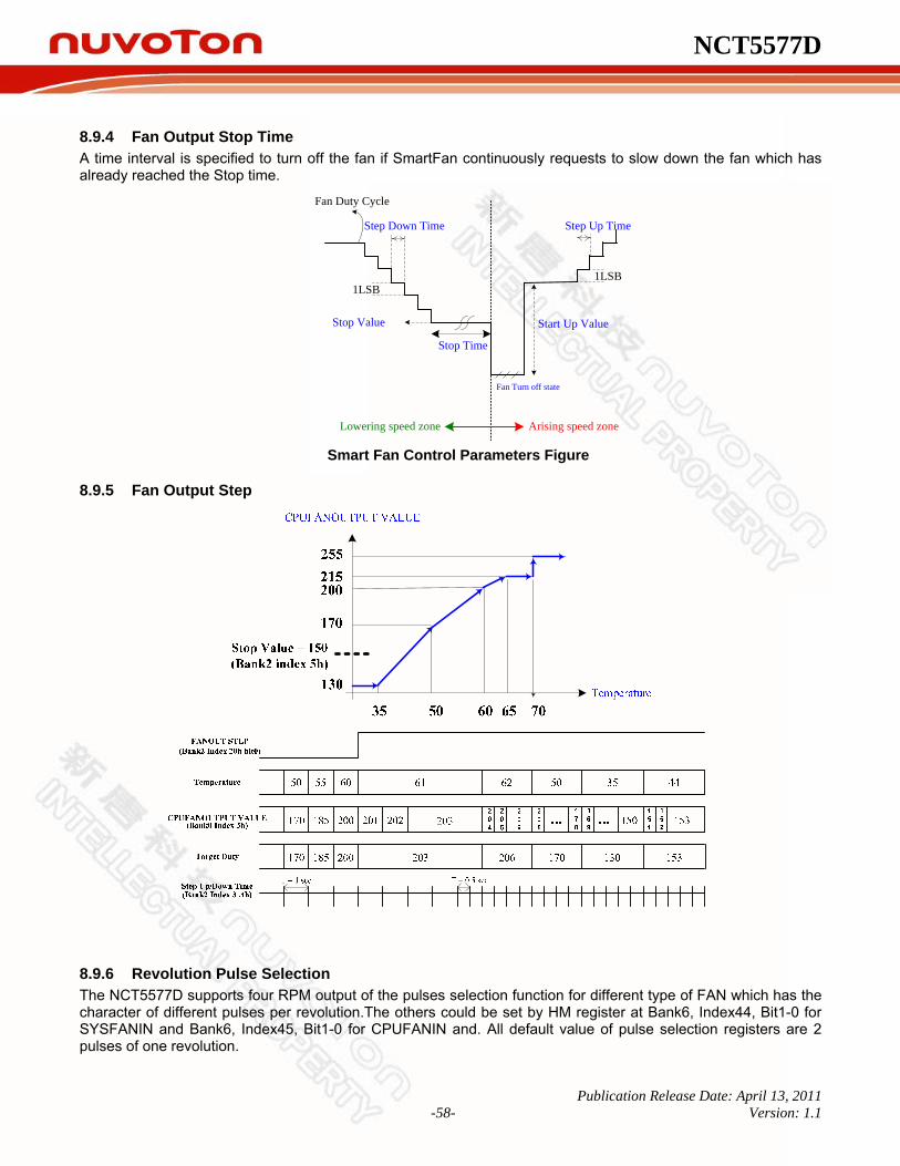
NCT5577D
Publication Release Date: April 13, 2011 -58- Version: 1.1
8.9.4 Fan Output Stop Time A time interval is specified to turn off the fan if SmartFan continuously requests to slow down the fan which has already reached the Stop time.
Lowering speed zone Arising speed zone
Fan Duty Cycle
Step Down Time Step Up Time
Stop Time
Stop Value
Fan Turn off state
Start Up Value
1LSB1LSB
Smart Fan Control Parameters Figure
8.9.5 Fan Output Step
8.9.6 Revolution Pulse Selection The NCT5577D supports four RPM output of the pulses selection function for different type of FAN which has the character of different pulses per revolution.The others could be set by HM register at Bank6, Index44, Bit1-0 for SYSFANIN and Bank6, Index45, Bit1-0 for CPUFANIN and. All default value of pulse selection registers are 2 pulses of one revolution.
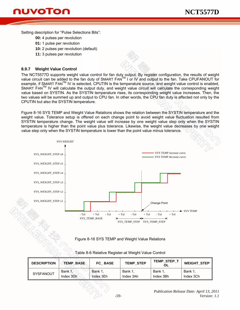
NCT5577D
Publication Release Date: April 13, 2011 -59- Version: 1.1
Setting description for “Pulse Selections Bits”: 00: 4 pulses per revolution 01: 1 pulse per revolution 10: 2 pulses per revolution (default) 11: 3 pulses per revolution
8.9.7 Weight Value Control The NCT5577D supports weight value control for fan duty output. By register configuration, the results of weight value circuit can be added to the fan duty of SMART FANTM I or IV and output to the fan. Take CPUFANOUT for example, if SMART FANTM IV is selected, CPUTIN is the temperature source, and weight value control is enabled, SMART FANTM IV will calculate the output duty, and weight value circuit will calculate the corresponding weight value based on SYSTIN. As the SYSTIN temperature rises, its corresponding weight value increases. Then, the two values will be summed up and output to CPU fan. In other words, the CPU fan duty is affected not only by the CPUTIN but also the SYSTIN temperature. Figure 8-16 SYS TEMP and Weight Value Relations shows the relation between the SYSTIN temperature and the weight value. Tolerance setup is offered on each change point to avoid weight value fluctuation resulted from SYSTIN temperature change. The weight value will increase by one weight value step only when the SYSTIN temperature is higher than the point value plus tolerance. Likewise, the weight value decreases by one weight value step only when the SYSTIN temperature is lower than the point value minus tolerance.
SYS_WEIGHT_STEP x1
SYS_WEIGHT_STEP x2
SYS_WEIGHT_STEP x3
SYS_WEIGHT_STEP x4
SYS_WEIGHT_STEP x5
SYS_WEIGHT_STEP x6
+ Tol- TolSYS_TEMP_BASE
+ Tol- Tol + Tol- Tol + Tol- Tol
SYS_TEMP_STEP SYS_TEMP_STEP
SYS TEMP
SYS WEIGHT
SYS TEMP increase curveSYS TEMP decrease curve
Change Point
Figure 8-16 SYS TEMP and Weight Value Relations
Table 8-6 Relative Register-at Weight Value Control
DESCRIPTION TEMP_BASE FC_ BASE TEMP_STEP TEMP_STEP_TOL WEIGHT_STEP
SYSFANOUT Bank 1, Index 3Dh
Bank 1, Index 3Eh
Bank 1, Index 3Ah
Bank 1, Index 3Bh
Bank 1, Index 3Ch

NCT5577D
Publication Release Date: April 13, 2011 -60- Version: 1.1
DESCRIPTION TEMP_BASE FC_ BASE TEMP_STEP TEMP_STEP_TOL WEIGHT_STEP
CPUFANOUT Bank 2, Index 3Dh
Bank 2, Index 3Eh
Bank 2, Index 3Ah
Bank 2, Index 3Bh
Bank 2, Index 3Ch
FAN CONTROL
LoadDefault Speed
Temperature Source SelectIndex 00 [4:0]
SF4 TableIndex 21~ 24Index 27 ~ 2A
Critical Temperature
Index 35
Critical Temperature
ToleranceIndex 38 [2:0]
Fan Control Weighting
Duty Mode
Step Up TimeIndex 03
Step Down Time
Index 04
Fanout StepIndex 20 [0]
MODEIndex 02 [7:4]
ToleranceIndex 02 [2:0]
WeightingConfiguration
Register
Temperature Step
Index 3A
Temperature Step Tolerance
Index 3B
Weight StepIndex 3C
Temperature Base
Index 3D
Temperature Fan Duty Base
Index 3E
Enable Weightingand Temperature
Source SelectIndex 39
Figure 8-17 Fan Control Weighting Duty Mode Programming Flow
8.10 Alert and Interrupt NCT5577D supports 6 Temperature Sensors for interrupt detection depending on selective monitor temperature source.
SMIOVT1 SMIOVT2 SMIOVT3 SMIOVT4 SMIOVT5 SMIOVT6 Temperature source select
Bank6, index21 bit[4:0]
Bank6, index22 bit[4:0]
Bank6, index23 bit[4:0]
Bank6, index24 bit[4:0]
Bank6, index25 bit[4:0]
Bank6, index26 bit[4:0]
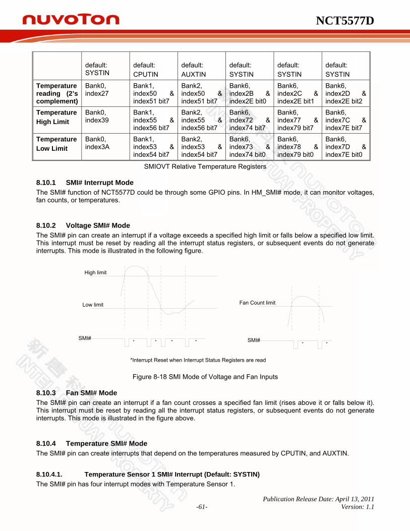
NCT5577D
Publication Release Date: April 13, 2011 -61- Version: 1.1
default: SYSTIN
default: CPUTIN
default: AUXTIN
default: SYSTIN
default: SYSTIN
default: SYSTIN
Temperature reading (2’s complement)
Bank0, index27
Bank1, index50 & index51 bit7
Bank2, index50 & index51 bit7
Bank6, index2B & index2E bit0
Bank6, index2C & index2E bit1
Bank6, index2D & index2E bit2
Temperature High Limit
Bank0, index39
Bank1, index55 & index56 bit7
Bank2, index55 & index56 bit7
Bank6, index72 & index74 bit7
Bank6, index77 & index79 bit7
Bank6, index7C & index7E bit7
Temperature Low Limit
Bank0, index3A
Bank1, index53 & index54 bit7
Bank2, index53 & index54 bit7
Bank6, index73 & index74 bit0
Bank6, index78 & index79 bit0
Bank6, index7D & index7E bit0
SMIOVT Relative Temperature Registers
8.10.1 SMI# Interrupt Mode The SMI# function of NCT5577D could be through some GPIO pins. In HM_SMI# mode, it can monitor voltages, fan counts, or temperatures.
8.10.2 Voltage SMI# Mode The SMI# pin can create an interrupt if a voltage exceeds a specified high limit or falls below a specified low limit. This interrupt must be reset by reading all the interrupt status registers, or subsequent events do not generate interrupts. This mode is illustrated in the following figure.
* * *
*Interrupt Reset when Interrupt Status Registers are read
SMI#*
High limit
Low limit
*SMI#
*
Fan Count limit
Figure 8-18 SMI Mode of Voltage and Fan Inputs
8.10.3 Fan SMI# Mode The SMI# pin can create an interrupt if a fan count crosses a specified fan limit (rises above it or falls below it). This interrupt must be reset by reading all the interrupt status registers, or subsequent events do not generate interrupts. This mode is illustrated in the figure above.
8.10.4 Temperature SMI# Mode The SMI# pin can create interrupts that depend on the temperatures measured by CPUTIN, and AUXTIN.
8.10.4.1. Temperature Sensor 1 SMI# Interrupt (Default: SYSTIN) The SMI# pin has four interrupt modes with Temperature Sensor 1.

NCT5577D
Publication Release Date: April 13, 2011 -62- Version: 1.1
(1) Shut-down Interrupt Mode This mode is enabled by setting Bank0 Index 40h, bit 4 to one. In this mode, the SMI# pin can create an interrupt when the current temperature rises above TOL or Shut-down mode high limit temperature, and when the current temperature falls below THYST or Shut-down mode low limit temperature. Once the temperature rises above TOL, however, and generates an interrupt, this mode does not generate additional interrupts, even if the temperature remains above TOL, until the temperature falls below THYST. This interrupt must be reset by reading all the interrupt status registers, or subsequent events do not generate interrupts, except the first time current temperature rises above Shut-down mode high limit temperature. This is illustrated in the following figure.
TOL
THTST
SMI#* * * * * * *
* Interrupt Reset when Interrupt Status Registers are read
Shut-down mode Low Limit Temperature
Shut-down mode High Limit Temperature
Figure 8-19 Shut-down Interrupt Mode
(2) Comparator Interrupt Mode
This mode is enabled by setting THYST (Temperature Hysteresis) to 127°C. This mode is enabled by setting Bank0 Index 40h, bit 4 to 0. In this mode, the SMI# pin can create an interrupt as long as the current temperature exceeds TO (Over Temperature). This interrupt can be reset by reading all the interrupt status registers, or subsequent events do not generate interrupts. If the interrupt is reset, the SMI# pin continues to create interrupts until the temperature goes below TO. This is illustrated in the figure below.
TOI
THYST
* *
*Interrupt Reset when Interrupt Status Registers are read
TOI
THYST
SMI# SMI#* * * **
127'C

NCT5577D
Publication Release Date: April 13, 2011 -63- Version: 1.1
Comparator Interrupt Mode Two-Times Interrupt Mode
Figure 8-20 SMI Mode of SYSTIN I
(3) Two-Times Interrupt Mode
This mode is enabled by setting THYST (Temperature Hysteresis) lower than TO and setting Bank0 Index 4Ch, bit 5 to zero. This mode is enabled by setting Bank0 Index 40h, bit 4 to 0. In this mode, the SMI# pin can create an interrupt when the current temperature rises above TO or when the current temperature falls below THYST. Once the temperature rises above TO, however, and generates an interrupt, this mode does not generate additional interrupts, even if the temperature remains above TO, until the temperature falls below THYST. This interrupt must be reset by reading all the interrupt status registers, or subsequent events do not generate interrupts. This is illustrated in the figure above.
(4) One-Time Interrupt Mode This mode is enabled by setting THYST (Temperature Hysteresis) lower than TO and setting Bank0 Index 4Ch, bit 5 to one. This mode is enabled by setting Bank0 Index 40h, bit 4 to 0. In this mode, the SMI# pin can create an interrupt when the current temperature rises above TO. Once the temperature rises above TO, however, and generates an interrupt, this mode does not generate additional interrupts, even if the temperature remains above TO, until the temperature falls below THYST. This interrupt must be reset by reading all the interrupt status registers, or subsequent events do not generate interrupts. This is illustrated in the following figure.
*Interrupt Reset when Interrupt Status Registers are read
TOI
THYST
SMI#* *
One-Time Interrupt Mode
Figure 8-21 SMI Mode of SYSTIN II
8.10.4.2. SMI# Interrupt of Temperature Sensor 2 (Default: CPUTIN) and Temperature Sensor 3 (Default: AUXTIN) and Temperature Sensor 4 (Default: SYSTIN) and Temperature Sensor 5 (Default: SYSTIN) and Temperature Sensor 6 (Default: SYSTIN). The SMI# pin has 3 interrupt modes with Temperature Sensor 2~6. (1) Shut-down Interrupt Mode
This mode is enabled by Bank0 Index 40h, bit5 to one for Temperature Sensor 2; Bank0 Index 40h, bit6 to one for Temperature Sensor 3; Bank6 Index 74h, bit1 to one for Temperature Sensor 4; Bank6 Index 79h, bit1 to one for Temperature Sensor 5 and Bank6 Index 7Eh, bit1 to one for Temperature Sensor 6.

NCT5577D
Publication Release Date: April 13, 2011 -64- Version: 1.1
In this mode, the SMI# pin can create an interrupt when the current temperature rises above TOL or Shut-down mode high limit temperature, and when the current temperature falls below THYST or Shut-down mode low limit temperature. Once the temperature rises above TOL, however, and generates an interrupt, this mode does not generate additional interrupts, even if the temperature remains above TOL, until the temperature falls below THYST. This interrupt must be reset by reading all the interrupt status registers, or subsequent events do not generate interrupts, except the first time current temperature rises above Shut-down mode high limit temperature. This is illustrated in the following figure.
TOL
THTST
SMI#* * * * * * *
* Interrupt Reset when Interrupt Status Registers are read
Shut-down mode Low Limit Temperature
Shut-down mode High Limit Temperature
Figure 8-22 Shut-down Interrupt Mode
(2) Comparator Interrupt Mode
This mode is enabled by setting Bank0 Index 4Ch, bit 6, to one. In this mode, the SMI# pin can create an interrupt when the current temperature exceeds TO (Over Temperature) and continues to create interrupts until the temperature falls below THYST. This interrupt can be reset by reading all the interrupt status registers, or subsequent events do not generate interrupts. This is illustrated in the figure below.
TOI
THYST
* * *
*Interrupt Reset when Interrupt Status Registers are read
TOI
THYST
SMI# SMI#* * * **
Comparator Interrupt Mode Two-Times Interrupt Mode
Figure 8-23 SMI Mode of CPUTIN
(3) Two-Times Interrupt Mode
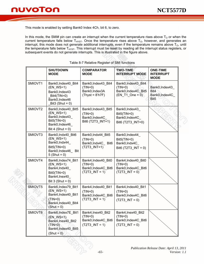
NCT5577D
Publication Release Date: April 13, 2011 -65- Version: 1.1
This mode is enabled by setting Bank0 Index 4Ch, bit 6, to zero. In this mode, the SMI# pin can create an interrupt when the current temperature rises above TO or when the current temperature falls below THYST. Once the temperature rises above TO, however, and generates an interrupt, this mode does not generate additional interrupts, even if the temperature remains above TO, until the temperature falls below THYST. This interrupt must be reset by reading all the interrupt status registers, or subsequent events do not generate interrupts. This is illustrated in the figure above.
Table 8-7 Relative Register of SMI functions
SHUTDOWN MODE
COMPARATOR MODE
TWO-TIME INTERRUPT MODE
ONE-TIME INTERRUPT MODE
SMIOVT1 Bank0,Index40_Bit4 (EN_WS=1) Bank0,Index43 _Bit4(TIN=0) Bank0,Index46 _Bit3 (Shut = 0)
Bank0,Index43_Bit4 (TIN=0) Bank0,Index3A (Thyst = 8’h7F)
Bank0,Index43_Bit4 (TIN=0) Bank0,Index4C_Bit5 (EN_T1_One = 0)
Bank0,Index43_Bit4 Bank0,Index4C_Bit5
SMIOVT2 Bank0,Index40_Bit5 (EN_WS=1) Bank0,Index43_ Bit5(TIN=0) Bank0,Index46_ Bit 4 (Shut = 0)
Bank0,Index43_Bit5(TIN=0) Bank0,Index4C_ Bit6 (T2T3_INT=1)
Bank0,Index43_ Bit5(TIN=0) Bank0,Index4C_ Bit6 (T2T3_INT=0)
SMIOVT3 Bank0,Indx40_Bit6 (EN_WS=1) Bank0,Indx44_ Bit5(TIN=0) Bank0,Index46_ Bit 5 (Shut = 0)
Bank0,Indx44_Bit5 (TIN=0) Bank0,Indx4C_ Bit6 (T2T3_INT=1)
Bank0,Index44_ Bit5(TIN=0) Bank0,Indx4C_ Bit6 (T2T3_INT = 0)
SMIOVT4 Bank6,Index74_Bit1 (EN_WS=1) Bank4,Indx40_ Bit0(TIN=0) Bank4,Inex40_ Bit 3 (Shut = 0)
Bank4,Index40_Bit0 (TIN=0) Bank0,Index4C_Bit6 (T2T3_INT = 1)
Bank4,Index40_Bit0 (TIN=0) Bank0,Index4C_Bit6 (T2T3_INT = 0)
SMIOVT5 Bank6,Index79_Bit1 (EN_WS=1) Bank4,Index40_Bit1 (TIN=0) Bank4,Index40_Bit4 (Shut = 0)
Bank4,Index40_Bit1(TIN=0) Bank0,Index4C_Bit6 (T2T3_INT = 1)
Bank4,Index40_Bit1 (TIN=0) Bank0,Index4C_Bit6 (T2T3_INT = 0)
SMIOVT6 Bank6,Index7E_Bit1 (EN_WS=1) Bank4,Inex40_Bit2 (TIN=0) Bank4,Index40_Bit5 (Shut = 0)
Bank4,Inex40_Bit2 (TIN=0) Bank0,Index4C_Bit6 (T2T3_INT = 1)
Bank4,Inex40_Bit2 (TIN=0) Bank0,Index4C_Bit6 (T2T3_INT = 0)

NCT5577D
Publication Release Date: April 13, 2011 -66- Version: 1.1
Table 8-8 Relative Register of OVT functions
SMIOVT1 SMIOVT2 SMIOVT3 Bank0,Index18_Bit6=0 (Enable OVT output) Bank0,Index18_Bit4 0: Comparator Mode (def.) 1: Interrupt Mode Bank0,Index18_Bit0 0: Start to monitor the source of SMIOVT1 temperature. 1: Stop monitoring the source of SMIOVT1 temperature.
Bank1, Index52_Bit0 0: Start to monitor the source of
SMIOVT2 temperature. 1: Stop monitoring the source of
SMIOVT2 temperature.
Bank 0, Inedex4C_Bit 3 0: Disable SMIOVT2
temperature sensor over temperature output
1: Enable SMIOVT2 temperature sensor over temperature output
Bank 1, Index52_Bit 1 0: Comparator Mode 1: Interrupt Mode
Bank 1, Index52_Bit 3~4 Number of faults to detect before setting OVT# output.
Bank2, Index52_Bit0 0: Start to monitor the source of
SMIOVT3 temperature. 1: Stop monitoring the source of
SMIOVT3 temperature.
Bank 0, Inedex4C_Bit 4 0: Disable SMIOVT3
temperature sensor over temperature output
1: Enable SMIOVT3 temperature sensor over temperature output
Bank 2, Index52_Bit 1 0: Comparator Mode 1: Interrupt Mode Bank 2, Index52_Bit3~4Number of faults to detect before setting OVT# output.
SMIOVT4 SMIOVT5 SMIOVT6 Bank6, Index28_Bit0 0: Start to monitor the source
of SMIOVT4 temperature. 1: Stop monitoring the source
of SMIOVT4 temperature.
Bank 6, Inedex74_Bit 2 0: Disable SMIOVT4
temperature sensor over temperature output
1: Enable SMIOVT4 temperature sensor over temperature output
Bank 6, Index28_Bit 1 0: Comparator Mode 1: Interrupt Mode Bank 6, Index28_Bit3~4
Number of faults to detect before setting OVT# output.
Bank6, Index29_Bit0 0: Start to monitor the source
of SMIOVT5 temperature. 1: Stop monitoring the source
of SMIOVT5 temperature.
Bank 6, Inedex79_Bit 2 0: Disable SMIOVT5
temperature sensor over temperature output
1: Enable SMIOVT5 temperature sensor over temperature output
Bank 6, Index29_Bit 1 0: Comparator Mode 1: Interrupt Mode Bank 6, Index29_Bit3~4Number of faults to detect before setting OVT# output.
Bank6, Index2A_Bit0 0: Start to monitor the source of
SMIOVT6 temperature. 1: Stop monitoring the source of
SMIOVT6 temperature.
Bank 6, Inedex7E_Bit 2 0: Disable SMIOVT6
temperature sensor over temperature output
1: Enable SMIOVT6 temperature sensor over temperature output
Bank 6, Index2A_Bit 1 0: Comparator Mode 1: Interrupt Mode Bank 6, Index2A_Bit3~4Number of faults to detect before setting OVT# output.
8.10.5 OVT# Interrupt Mode
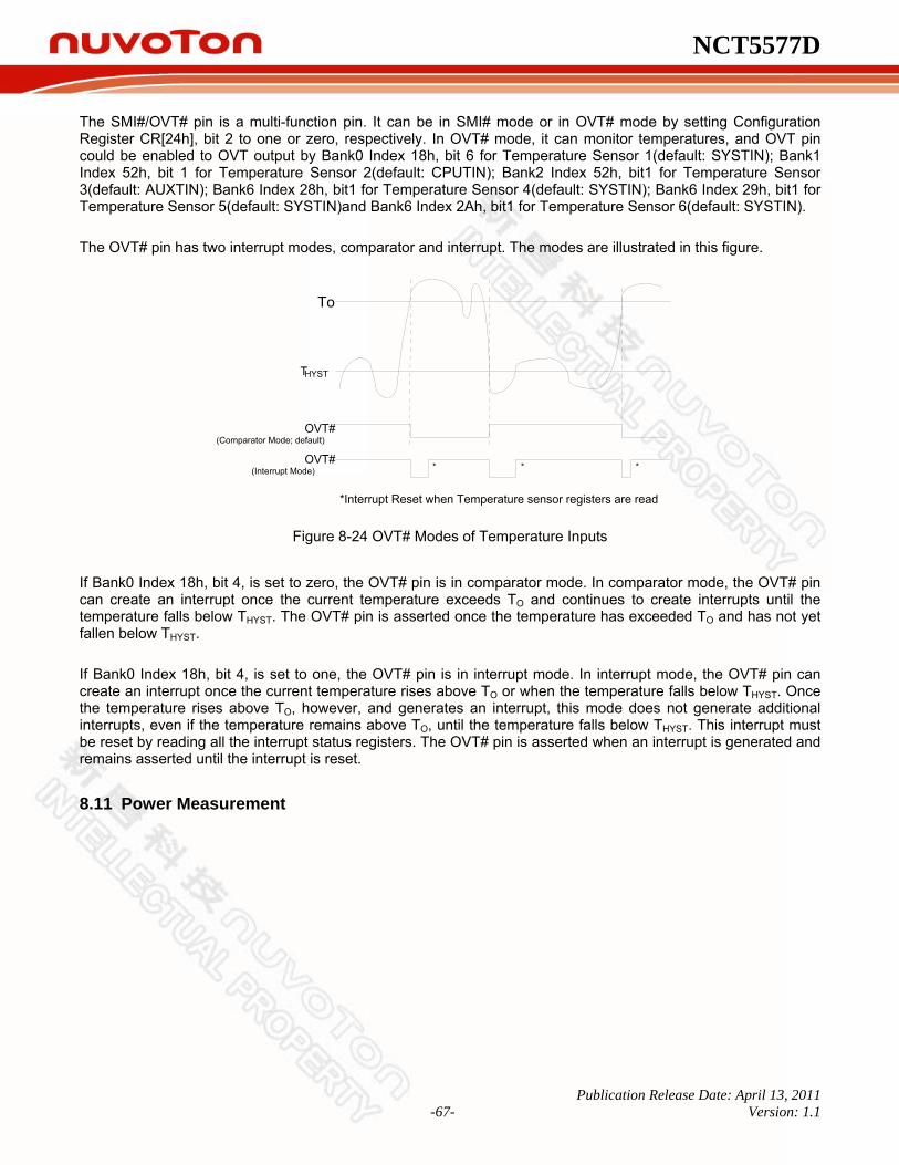
NCT5577D
Publication Release Date: April 13, 2011 -67- Version: 1.1
The SMI#/OVT# pin is a multi-function pin. It can be in SMI# mode or in OVT# mode by setting Configuration Register CR[24h], bit 2 to one or zero, respectively. In OVT# mode, it can monitor temperatures, and OVT pin could be enabled to OVT output by Bank0 Index 18h, bit 6 for Temperature Sensor 1(default: SYSTIN); Bank1 Index 52h, bit 1 for Temperature Sensor 2(default: CPUTIN); Bank2 Index 52h, bit1 for Temperature Sensor 3(default: AUXTIN); Bank6 Index 28h, bit1 for Temperature Sensor 4(default: SYSTIN); Bank6 Index 29h, bit1 for Temperature Sensor 5(default: SYSTIN)and Bank6 Index 2Ah, bit1 for Temperature Sensor 6(default: SYSTIN). The OVT# pin has two interrupt modes, comparator and interrupt. The modes are illustrated in this figure.
THYST
* *
*Interrupt Reset when Temperature sensor registers are read
OVT#
OVT#
*
(Comparator Mode; default)
(Interrupt Mode)
To
Figure 8-24 OVT# Modes of Temperature Inputs
If Bank0 Index 18h, bit 4, is set to zero, the OVT# pin is in comparator mode. In comparator mode, the OVT# pin can create an interrupt once the current temperature exceeds TO and continues to create interrupts until the temperature falls below THYST. The OVT# pin is asserted once the temperature has exceeded TO and has not yet fallen below THYST. If Bank0 Index 18h, bit 4, is set to one, the OVT# pin is in interrupt mode. In interrupt mode, the OVT# pin can create an interrupt once the current temperature rises above TO or when the temperature falls below THYST. Once the temperature rises above TO, however, and generates an interrupt, this mode does not generate additional interrupts, even if the temperature remains above TO, until the temperature falls below THYST. This interrupt must be reset by reading all the interrupt status registers. The OVT# pin is asserted when an interrupt is generated and remains asserted until the interrupt is reset.
8.11 Power Measurement
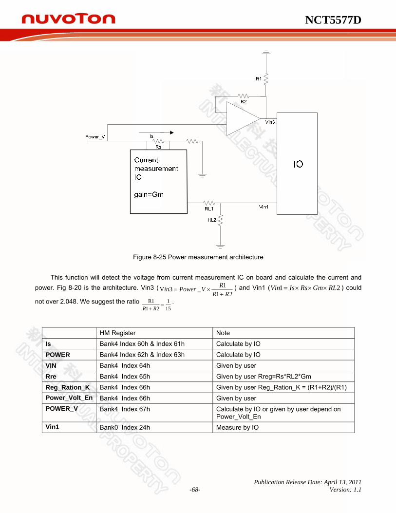
NCT5577D
Publication Release Date: April 13, 2011 -68- Version: 1.1
Figure 8-25 Power measurement architecture
This function will detect the voltage from current measurement IC on board and calculate the current and
power. Fig 8-20 is the architecture. Vin3 (21
1_3VRR
RVPowerin+
×= ) and Vin1 ( 21 RLGmRsIsVin ×××= ) could
not over 2.048. We suggest the ratio 151
211R
=+ RR
.
HM Register Note
Is Bank4 Index 60h & Index 61h Calculate by IO
POWER Bank4 Index 62h & Index 63h Calculate by IO
VIN Bank4 Index 64h Given by user
Rre Bank4 Index 65h Given by user Rreg=Rs*RL2*Gm
Reg_Ration_K Bank4 Index 66h Given by user Reg_Ration_K = (R1+R2)/(R1) Power_Volt_En Bank4 Index 66h Given by user POWER_V Bank4 Index 67h Calculate by IO or given by user depend on
Power_Volt_En Vin1 Bank0 Index 24h Measure by IO

NCT5577D
Publication Release Date: April 13, 2011 -69- Version: 1.1
9. HARDWARE MONITOR REGISTER SET The base address of the Address Port and Data Port is specified in registers CR[60h] and CR[61h] of Logical Device B, the hardware monitor device. CR[60h] is the high byte, and CR[61h] is the low byte. The Address Port and Data Port are located at the base address, plus 5h and 6h, respectively. For example, if CR[60h] is 02h and CR[61h] is 90h, the Address Port is at 0x295h, and the Data Port is at 0x296h. Remember that this access is from the host CPU I/O address range. To conserve space in the crowded CPU I/O addresses, many of the hardware monitor registers are “banked” with the bank number located at Bank0, index 04Eh.
9.1 Address Port (Port x5h) Attribute: Bit 6:0 Read/Write , Bit 7: Reserved Size: 8 bits
BIT 7 6 5 4 3 2 1 0 NAME DATA
DEFAULT 0 0 0 0 0 0 0 0
BIT DESCRIPTION
7 RESERVED. 6-0 READ/WRITE.
BIT 7 BIT 6 BIT 5 BIT 4 BIT 3 BIT 2 BIT 1 BIT 0
Reserved Address Pointer (Power On default 00h)
(Power On default 0) A6 A5 A4 A3 A2 A1 A0
9.2 Data Port (Port x6h) Attribute: Read/Write Size: 8 bits
BIT 7 6 5 4 3 2 1 0
NAME DATA
DEFAULT 0 0 0 0 0 0 0 0
BIT DESCRIPTION
7-0 Data to be read from or to be written to Value RAM and Register.
9.3 SYSFANOUT PWM Output Frequency Configuration Register – Index 00h (Bank 0) Attribute: Read/Write Size: 8 bits
BIT 7 6 5 4 3 2 1 0

NCT5577D
Publication Release Date: April 13, 2011 -70- Version: 1.1
NAME PWM_CLK_SEL1 PWM_SCALE1
DEFAULT 0 0 0 0 0 1 0 0
The register is meaningful only when SYSFANOUT is progarmmed for PWM output (i.e., Bank0, Index 04h, bit 0 is 0).
BIT DESCRIPTION
7
PWM_CLK_SEL1. SYSFANOUT PWM Input Clock Source Select. This bit selects the clock source for PWM output frequency. 0: The clock source is 24 MHz. 1: The clock source is 258 KHz.
6-0
PWM_SCALE1. SYSFANOUT PWM Pre-Scale divider. The clock source for PWM output is divided by this seven-bit value to calculate the actual PWM output frequency.
PWM output frequency = 2561
Divider Pre_ScaleClockInput
∗
The maximum value of the divider is 127 (7Fh), and it should not be set to 0.
The clock source selected by CKSEL will be divided by the divisor and used as a fan PWM output frequency. If CKSEL equals 0, then the output clock is simply equal to 93.9/ (Divisor[6:0]+1) KHz MappedDivisor depends on Divisor[6:0] and is described in the table below.
Divisor[6:0] Mapped Divisor Output Frequency Divisor[6:0] Mapped Divisor Output Frequency
0000000 1 93.9KHz
0000001 2 46.95KHz
0000010 3 31.3KHz
0000011 4 23.47KHz
…………………………………………..
0000100 5 18.78KHz 0001111 16 5.86KHz
0000101 6 15.65KHz 0011111 32 2.93KHz
0000110 7 13.41KHz 0111111 64 1.46KHz
0000111 8 11.73KHz 1111111 128 734Hz
If CKSEL equals 1, then the output clock is simply equal to 1008/ Mapped Divisor Hz MappedDivisor depends on Divisor[3:0] and is described in the table below.
Divisor[3:0] Mapped Divisor Output Frequency Divisor[3:0] Mapped Divisor Output Frequency
0000 1 1008Hz 1000 12 84Hz
0001 2 504Hz 1001 16 63Hz
0010 3 336Hz 1010 32 31.5Hz
0011 4 252Hz 1011 64 15.75Hz
0100 5 201Hz 1100 128 7.875Hz
0101 6 168Hz 1101 256 3.94Hz
0110 7 144Hz 1110 512 1.97Hz
0111 8 126Hz 1111 1024 0.98Hz
9.4 SYSFANOUT Output Value Select Register – Index 01h (Bank 0) Attribute: Read Only Size: 8 bits

NCT5577D
Publication Release Date: April 13, 2011 -71- Version: 1.1
BIT 7 6 5 4 3 2 1 0 NAME SYSFANOUT Value
DEFAULT FFh
FUNCTION MODE 7 6 5 4 3 2 1 0 PWM Output (Bank0, Index 04h, bit 0 is 0)
DESCRIPTION The PWM duty cycle is equal to this eight-bit value, divided by 255, times 100%. FFh creates a duty cycle of 100%, and 00h creates a duty cycle of 0%.
DC Voltage Output Bank0, Index 04h, bit 0 is 1) DESCRIPTION
SYSFANOUT voltage control. The output voltage is calculated according to this equation.
OUTPUT Voltage = 64
* FANOUTVref
Note. VREF is approx 2.048V.
Reserved
This register could be programmed by Bank1, Index 09
9.5 CPUFANOUT PWM Output Frequency Configuration Register – Index 02h (Bank 0) Attribute: Read/Write Size: 8 bits
BIT 7 6 5 4 3 2 1 0
NAME PWM_CLK_SEL2 PWM_SCALE2
DEFAULT 0 0 0 0 0 1 0 0
The register is meaningful only when CPUFANOUT is programmed for PWM output.
BIT DESCRIPTION
7
PWM_CLK_SEL2. CPUFANOUT PWM Input Clock Source Select. This bit selects the clock source for the PWM output. 0: The clock source is 24 MHz. 1: The clock source is 258 KHz.
6-0
PWM_SCALE2. CPUFANOUT PWM Pre-Scale divider. The clock source for PWM output is divided by this seven-bit value to calculate the actual PWM output frequency.
PWM output frequency = 2561
Divider Pre_ScaleClockInput
∗
The maximum value of the divider is 127 (7Fh), and it should not be set to 0.
The clock source selected by CKSEL will be divided by the divisor and used as a fan PWM output frequency. If CKSEL equals 0, then the output clock is simply equal to 93.9/ (Divisor[6:0]+1) KHz MappedDivisor depends on Divisor[6:0] and is described in the table below.
Divisor[6:0] Mapped Divisor Output Frequency Divisor[6:0] Mapped Divisor Output Frequency
0000000 1 93.9KHz
0000001 2 46.95KHz
0000010 3 31.3KHz
0000011 4 23.47KHz
…………………………………………..

NCT5577D
Publication Release Date: April 13, 2011 -72- Version: 1.1
Divisor[6:0] Mapped Divisor Output Frequency Divisor[6:0] Mapped Divisor Output Frequency
0000100 5 18.78KHz 0001111 16 5.86KHz
0000101 6 15.65KHz 0011111 32 2.93KHz
0000110 7 13.41KHz 0111111 64 1.46KHz
0000111 8 11.73KHz 1111111 128 734Hz
If CKSEL equals 1, then the output clock is simply equal to 1008/ Mapped Divisor Hz MappedDivisor depends on Divisor[3:0] and is described in the table below.
Divisor[3:0] Mapped Divisor Output Frequency Divisor[3:0] Mapped Divisor Output Frequency
0000 1 1008Hz 1000 12 84Hz
0001 2 504Hz 1001 16 63Hz
0010 3 336Hz 1010 32 31.5Hz
0011 4 252Hz 1011 64 15.75Hz
0100 5 201Hz 1100 128 7.875Hz
0101 6 168Hz 1101 256 3.94Hz
0110 7 144Hz 1110 512 1.97Hz
0111 8 126Hz 1111 1024 0.98Hz
9.6 CPUFANOUT Output Value Select Register – Index 03h (Bank 0) Attribute: Read Only Size: 8 bits
BIT 7 6 5 4 3 2 1 0
NAME CPUFANOUT Value
DEFAULT 7Fh
FUNCTION MODE 7 6 5 4 3 2 1 0
PWM Output DESCRIPTION CPUFANOUT PWM Duty. The PWM duty cycle is equal to this 8-bit value, divided by 255, times 100%. FFh creates a duty cycle of 100%, and creates a duty cycle of 0%.
This register could be programmed by Bank2, Index 09
9.7 SYSFANOUT Configuration Register I – Index 04h (Bank 0) Attribute: Read/Write Size: 8 bits
BIT 7 6 5 4 3 2 1 0
NAME RESERVED SYSFANOUT_SEL
DEFAULT 0 0 0 0 0 0 0 1
BIT DESCRIPTION
7-1 Reserved.
0 SYSFANOUT Output Mode Selection. 0: SYSFANOUT pin produces a PWM duty cycle output.

NCT5577D
Publication Release Date: April 13, 2011 -73- Version: 1.1
BIT DESCRIPTION 1: SYSFANOUT pin produces DC output. (Default)
9.8 Reserved Register – Index 05h ~ 0Fh (Bank 0)
9.9 Reserved Register – Index 10h (Bank 0)
9.10 Reserved Register – Index 11h (Bank 0)
9.11 Reserved Register – Index 12-17h (Bank 0)
9.12 OVT# Configuration Register – Index 18h (Bank 0) Attribute: Read/Write Size: 8 bits
BIT 7 6 5 4 3 2 1 0
BIT RESERVED DIS_OVT1 RESERVED OVT1_Mode RESERVED STOP
DEFAULT 0 1 0 0 0 0 0 0
BIT DESCRIPTION
7 Reserved.
6 DIS_OVT1. 0: Enable SMIOVT1 OVT# output. (Default) 1: Disable temperature sensor SMIOVT1 over-temperature (OVT#) output.
5 Reserved.
4 OVT1_Mode. SMIOVT1 Mode Select. 0: Compare Mode. (Default) 1: Interrupt Mode.
3-1 Reserved.
0 STOP. 0: Monitor SMIOVT1 temperature source. 1: Stop monitoring SMIOVT1 temperature source.
9.13 Reserved Registers – Index 19h ~ 1Fh (Bank 0)
9.14 Value RAM ⎯ Index 20h ~ 3Fh (Bank 0) ADDRESS A6-A0 DESCRIPTION
20h CPUVCORE reading
21h VIN0 reading
22h AVCC reading
23h 3VCC reading
24h VIN1 reading
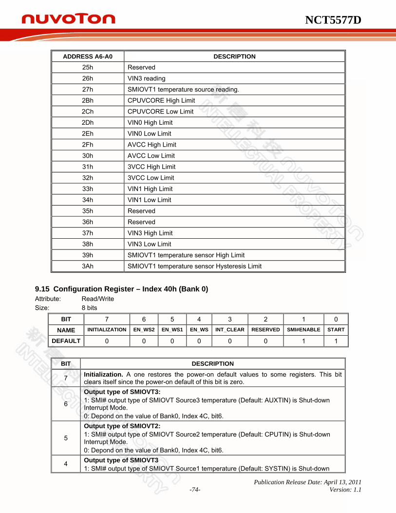
NCT5577D
Publication Release Date: April 13, 2011 -74- Version: 1.1
ADDRESS A6-A0 DESCRIPTION
25h Reserved
26h VIN3 reading
27h SMIOVT1 temperature source reading.
2Bh CPUVCORE High Limit
2Ch CPUVCORE Low Limit
2Dh VIN0 High Limit
2Eh VIN0 Low Limit
2Fh AVCC High Limit
30h AVCC Low Limit
31h 3VCC High Limit
32h 3VCC Low Limit
33h VIN1 High Limit
34h VIN1 Low Limit
35h Reserved
36h Reserved
37h VIN3 High Limit
38h VIN3 Low Limit
39h SMIOVT1 temperature sensor High Limit
3Ah SMIOVT1 temperature sensor Hysteresis Limit
9.15 Configuration Register – Index 40h (Bank 0) Attribute: Read/Write Size: 8 bits
BIT 7 6 5 4 3 2 1 0
NAME INITIALIZATION EN_WS2 EN_WS1 EN_WS INT_CLEAR RESERVED SMI#ENABLE START
DEFAULT 0 0 0 0 0 0 1 1
BIT DESCRIPTION
7 Initialization. A one restores the power-on default values to some registers. This bit clears itself since the power-on default of this bit is zero.
6
Output type of SMIOVT3: 1: SMI# output type of SMIOVT Source3 temperature (Default: AUXTIN) is Shut-down Interrupt Mode. 0: Depond on the value of Bank0, Index 4C, bit6.
5
Output type of SMIOVT2: 1: SMI# output type of SMIOVT Source2 temperature (Default: CPUTIN) is Shut-down Interrupt Mode. 0: Depond on the value of Bank0, Index 4C, bit6.
4 Output type of SMIOVT3 1: SMI# output type of SMIOVT Source1 temperature (Default: SYSTIN) is Shut-down
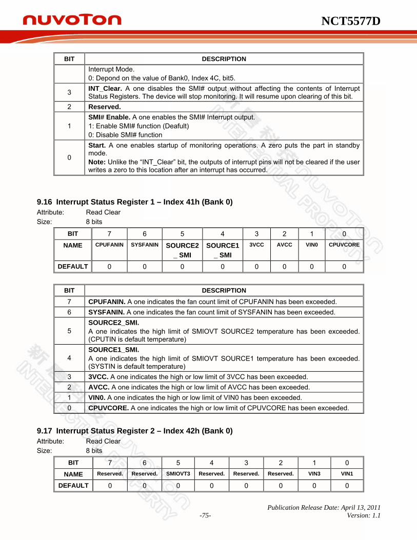
NCT5577D
Publication Release Date: April 13, 2011 -75- Version: 1.1
BIT DESCRIPTION Interrupt Mode. 0: Depond on the value of Bank0, Index 4C, bit5.
3 INT_Clear. A one disables the SMI# output without affecting the contents of Interrupt Status Registers. The device will stop monitoring. It will resume upon clearing of this bit.
2 Reserved.
1 SMI# Enable. A one enables the SMI# Interrupt output. 1: Enable SMI# function (Deafult) 0: Disable SMI# function
0
Start. A one enables startup of monitoring operations. A zero puts the part in standby mode. Note: Unlike the “INT_Clear” bit, the outputs of interrupt pins will not be cleared if the user writes a zero to this location after an interrupt has occurred.
9.16 Interrupt Status Register 1 – Index 41h (Bank 0) Attribute: Read Clear Size: 8 bits
BIT 7 6 5 4 3 2 1 0
NAME CPUFANIN SYSFANIN SOURCE2_ SMI
SOURCE1_ SMI
3VCC AVCC VIN0 CPUVCORE
DEFAULT 0 0 0 0 0 0 0 0
BIT DESCRIPTION
7 CPUFANIN. A one indicates the fan count limit of CPUFANIN has been exceeded. 6 SYSFANIN. A one indicates the fan count limit of SYSFANIN has been exceeded.
5 SOURCE2_SMI. A one indicates the high limit of SMIOVT SOURCE2 temperature has been exceeded. (CPUTIN is default temperature)
4 SOURCE1_SMI. A one indicates the high limit of SMIOVT SOURCE1 temperature has been exceeded. (SYSTIN is default temperature)
3 3VCC. A one indicates the high or low limit of 3VCC has been exceeded. 2 AVCC. A one indicates the high or low limit of AVCC has been exceeded. 1 VIN0. A one indicates the high or low limit of VIN0 has been exceeded. 0 CPUVCORE. A one indicates the high or low limit of CPUVCORE has been exceeded.
9.17 Interrupt Status Register 2 – Index 42h (Bank 0) Attribute: Read Clear Size: 8 bits
BIT 7 6 5 4 3 2 1 0
NAME Reserved. Reserved. SMIOVT3 Reserved. Reserved. Reserved. VIN3 VIN1
DEFAULT 0 0 0 0 0 0 0 0
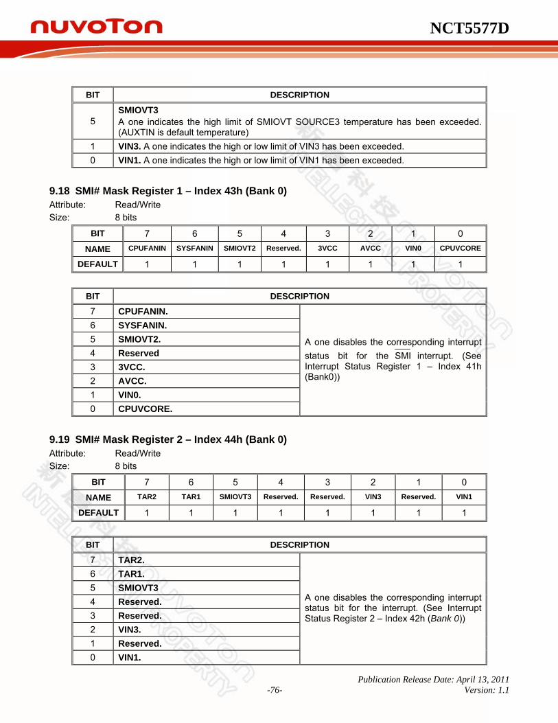
NCT5577D
Publication Release Date: April 13, 2011 -76- Version: 1.1
BIT DESCRIPTION
5 SMIOVT3 A one indicates the high limit of SMIOVT SOURCE3 temperature has been exceeded. (AUXTIN is default temperature)
1 VIN3. A one indicates the high or low limit of VIN3 has been exceeded. 0 VIN1. A one indicates the high or low limit of VIN1 has been exceeded.
9.18 SMI# Mask Register 1 – Index 43h (Bank 0) Attribute: Read/Write Size: 8 bits
BIT 7 6 5 4 3 2 1 0
NAME CPUFANIN SYSFANIN SMIOVT2 Reserved. 3VCC AVCC VIN0 CPUVCORE
DEFAULT 1 1 1 1 1 1 1 1
BIT DESCRIPTION
7 CPUFANIN. 6 SYSFANIN. 5 SMIOVT2. 4 Reserved 3 3VCC. 2 AVCC. 1 VIN0. 0 CPUVCORE.
A one disables the corresponding interrupt status bit for the SMI interrupt. (See Interrupt Status Register 1 – Index 41h (Bank0))
9.19 SMI# Mask Register 2 – Index 44h (Bank 0) Attribute: Read/Write Size: 8 bits
BIT 7 6 5 4 3 2 1 0
NAME TAR2 TAR1 SMIOVT3 Reserved. Reserved. VIN3 Reserved. VIN1
DEFAULT 1 1 1 1 1 1 1 1
BIT DESCRIPTION
7 TAR2. 6 TAR1. 5 SMIOVT3 4 Reserved. 3 Reserved. 2 VIN3. 1 Reserved. 0 VIN1.
A one disables the corresponding interrupt status bit for the interrupt. (See Interrupt Status Register 2 – Index 42h (Bank 0))

NCT5577D
Publication Release Date: April 13, 2011 -77- Version: 1.1
9.20 Interrupt Status Register 4 – Index 45h (Bank 0) Attribute: Read Clear Size: 8 bits
BIT 7 6 5 4 3 2 1 0 NAME Reserved. Reserved. Reserved. CPU
FANOUTSYS
FANOUTShut_
SOURCE3_SMIShut_
SOURCE2_SMI Shut_
SOURCE1_SMI
DEFAULT 0 0 0 0 0 0 0 0
BIT DESCRIPTION
7 Reserved. 6 Reserved. 5 Reserved.
4 CPUFANOUT. “1” indicates that CPUFANOUT works for three minutes at the full fan speed.
3 SYSFANOUT. “1” indicates that SYSFANOUT works for three minutes at the full fan speed.
2 Shut_SOURCE3_SMI. “1” indicates the high limit of SMIOVT_SOURCE3 temperature of SMI# Shut-down mode has been exceeded. (AUXTIN is default temperature)
1 Shut_SOURCE2_SMI. “1” indicates the high limit of SMIOVT _SOURCE2 temperature of SMI# Shut-down mode has been exceeded. (CPUTIN is default temperature)
0 Shut_SOURCE1_SMI. “1” indicates the high limit of SMIOVT _SOURCE1 temperature of SMI# Shut-down mode has been exceeded. (SYSTIN is default temperature)
9.21 SMI# Mask Register 3 – Index 46h (Bank 0) Attribute: Read/Write Size: 8 bits
BIT 7 6 5 4 3 2 1 0
NAME Reserved. Reserved. Shut_AUX Shut_CPU Shut_SYS Reserved. Reserved. Reserved.
DEFAULT 0 0 1 1 1 1 1 0
BIT DESCRIPTION
7 Reserved. 6 Reserved. 5 Shut_AUX 4 Shut_CPU
3 Shut_SYS
“1” disables the corresponding interrupt status bit for the SMI interrupt. (See Interrupt Status Register 4 – Index 45h (Bank 0)).
2 Reserved. “1” disables the corresponding interrupt status bit for the SMI interrupt.
1 Reserved. “1” disables the corresponding interrupt status bit for the SMI interrupt
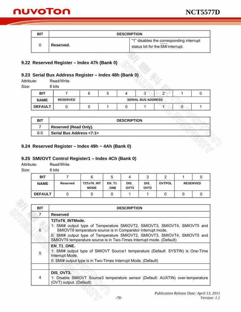
NCT5577D
Publication Release Date: April 13, 2011 -78- Version: 1.1
BIT DESCRIPTION
0 Reserved. “1” disables the corresponding interrupt status bit for the SMI interrupt.
9.22 Reserved Register – Index 47h (Bank 0)
9.23 Serial Bus Address Register – Index 48h (Bank 0) Attribute: Read/Write Size: 8 bits
BIT 7 6 5 4 3 2 1 0
NAME RESERVED SERIAL BUS ADDRESS
DEFAULT 0 0 1 0 1 1 0 1
BIT DESCRIPTION
7 Reserved (Read Only). 6-0 Serial Bus Address <7:1>
9.24 Reserved Register – Index 49h ~ 4Ah (Bank 0)
9.25 SMI/OVT Control Register1 – Index 4Ch (Bank 0) Attribute: Read/Write Size: 8 bits
BIT 7 6 5 4 3 2 1 0 NAME Reserved T2ToT6_INT
MODE EN_T1 _ONE
DIS_ OVT3
DIS_ OVT2
OVTPOL RESERVED
DEFAULT 0 0 0 1 1 0 0 0
BIT DESCRIPTION
7 Reserved
6
T2ToT6_INTMode. 1: SMI# output type of Temperature SMIOVT2, SMIOVT3, SMIOVT4, SMIOVT5 and
SMIOVT6 temperature source is in Comparator Interrupt mode. 0: SMI# output type of Temperature SMIOVT2, SMIOVT3, SMIOVT4, SMIOVT5 and SMIOVT6 temperature source is in Two-Times Interrupt mode. (Default)
5
EN_T1_ONE. 1: SMI# output type of SMIOVT Source1 temperature (Default: SYSTIN) is One-Time Interrupt Mode. 0: SMI# output type is in Two-Times Interrupt Mode. (Default)
4 DIS_OVT3. 1: Disable SMIOVT Source3 temperature sensor (Default: AUXTIN) over-temperature (OVT) output. (Default)
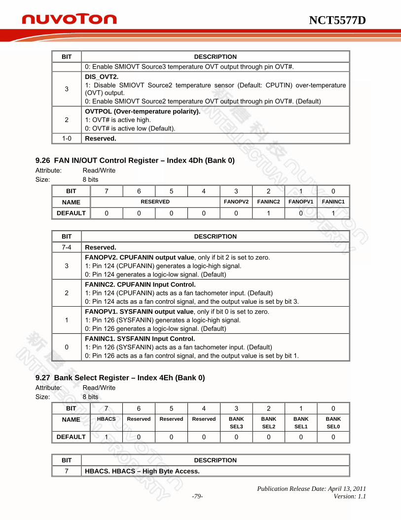
NCT5577D
Publication Release Date: April 13, 2011 -79- Version: 1.1
BIT DESCRIPTION 0: Enable SMIOVT Source3 temperature OVT output through pin OVT#.
3
DIS_OVT2. 1: Disable SMIOVT Source2 temperature sensor (Default: CPUTIN) over-temperature (OVT) output. 0: Enable SMIOVT Source2 temperature OVT output through pin OVT#. (Default)
2 OVTPOL (Over-temperature polarity). 1: OVT# is active high. 0: OVT# is active low (Default).
1-0 Reserved.
9.26 FAN IN/OUT Control Register – Index 4Dh (Bank 0) Attribute: Read/Write Size: 8 bits
BIT 7 6 5 4 3 2 1 0
NAME RESERVED FANOPV2 FANINC2 FANOPV1 FANINC1
DEFAULT 0 0 0 0 0 1 0 1
BIT DESCRIPTION
7-4 Reserved.
3 FANOPV2. CPUFANIN output value, only if bit 2 is set to zero. 1: Pin 124 (CPUFANIN) generates a logic-high signal. 0: Pin 124 generates a logic-low signal. (Default)
2 FANINC2. CPUFANIN Input Control. 1: Pin 124 (CPUFANIN) acts as a fan tachometer input. (Default) 0: Pin 124 acts as a fan control signal, and the output value is set by bit 3.
1 FANOPV1. SYSFANIN output value, only if bit 0 is set to zero. 1: Pin 126 (SYSFANIN) generates a logic-high signal. 0: Pin 126 generates a logic-low signal. (Default)
0 FANINC1. SYSFANIN Input Control. 1: Pin 126 (SYSFANIN) acts as a fan tachometer input. (Default) 0: Pin 126 acts as a fan control signal, and the output value is set by bit 1.
9.27 Bank Select Register – Index 4Eh (Bank 0) Attribute: Read/Write Size: 8 bits
BIT 7 6 5 4 3 2 1 0
NAME HBACS Reserved Reserved Reserved BANK SEL3
BANK SEL2
BANK SEL1
BANK SEL0
DEFAULT 1 0 0 0 0 0 0 0
BIT DESCRIPTION
7 HBACS. HBACS – High Byte Access.
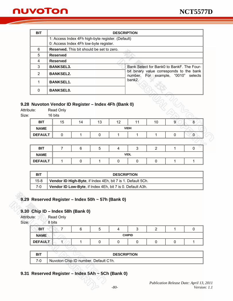
NCT5577D
Publication Release Date: April 13, 2011 -80- Version: 1.1
BIT DESCRIPTION 1: Access Index 4Fh high-byte register. (Default) 0: Access Index 4Fh low-byte register.
6 Reserved. This bit should be set to zero. 5 Reserved 4 Reserved 3 BANKSEL3.
2 BANKSEL2.
1 BANKSEL1.
0 BANKSEL0.
Bank Select for Bank0 to BankF. The Four-bit binary value corresponds to the bank number. For example, “0010” selects bank2.
9.28 Nuvoton Vendor ID Register – Index 4Fh (Bank 0) Attribute: Read Only Size: 16 bits
BIT 15 14 13 12 11 10 9 8
NAME VIDH
DEFAULT 0 1 0 1 1 1 0 0
BIT 7 6 5 4 3 2 1 0
NAME VIDL
DEFAULT 1 0 1 0 0 0 1 1
BIT DESCRIPTION
15-8 Vendor ID High-Byte, if Index 4Eh, bit 7 is 1. Default 5Ch. 7-0 Vendor ID Low-Byte, if Index 4Eh, bit 7 is 0. Default A3h.
9.29 Reserved Register – Index 50h ~ 57h (Bank 0)
9.30 Chip ID – Index 58h (Bank 0) Attribute: Read Only Size: 8 bits
BIT 7 6 5 4 3 2 1 0
NAME CHIPID
DEFAULT 1 1 0 0 0 0 0 1
BIT DESCRIPTION
7-0 Nuvoton Chip ID number. Default C1h.
9.31 Reserved Register – Index 5Ah ~ 5Ch (Bank 0)
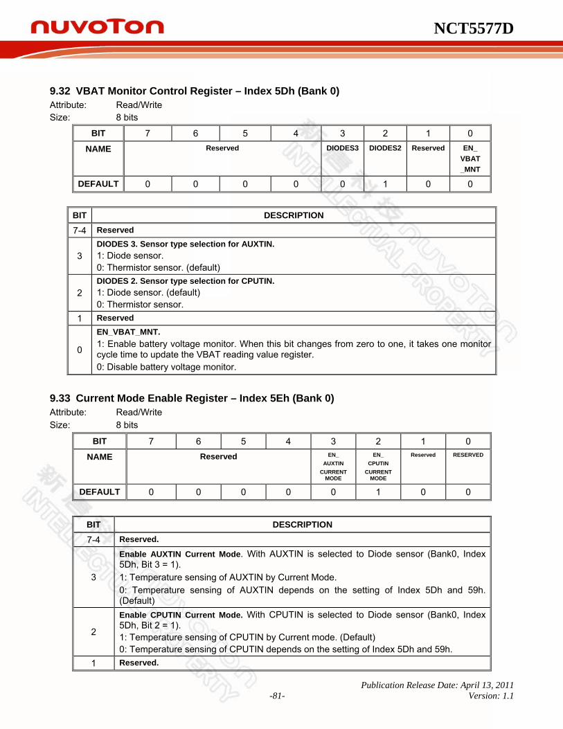
NCT5577D
Publication Release Date: April 13, 2011 -81- Version: 1.1
9.32 VBAT Monitor Control Register – Index 5Dh (Bank 0) Attribute: Read/Write Size: 8 bits
BIT 7 6 5 4 3 2 1 0
NAME Reserved
DIODES3 DIODES2 Reserved EN_ VBAT _MNT
DEFAULT 0 0 0 0 0 1 0 0
BIT DESCRIPTION
7-4 Reserved
3 DIODES 3. Sensor type selection for AUXTIN. 1: Diode sensor. 0: Thermistor sensor. (default)
2 DIODES 2. Sensor type selection for CPUTIN. 1: Diode sensor. (default) 0: Thermistor sensor.
1 Reserved
0
EN_VBAT_MNT. 1: Enable battery voltage monitor. When this bit changes from zero to one, it takes one monitor cycle time to update the VBAT reading value register. 0: Disable battery voltage monitor.
9.33 Current Mode Enable Register – Index 5Eh (Bank 0) Attribute: Read/Write Size: 8 bits
BIT 7 6 5 4 3 2 1 0 NAME Reserved EN_
AUXTIN CURRENT
MODE
EN_ CPUTIN
CURRENT MODE
Reserved RESERVED
DEFAULT 0 0 0 0 0 1 0 0
BIT DESCRIPTION
7-4 Reserved.
3
Enable AUXTIN Current Mode. With AUXTIN is selected to Diode sensor (Bank0, Index 5Dh, Bit 3 = 1). 1: Temperature sensing of AUXTIN by Current Mode. 0: Temperature sensing of AUXTIN depends on the setting of Index 5Dh and 59h. (Default)
2
Enable CPUTIN Current Mode. With CPUTIN is selected to Diode sensor (Bank0, Index 5Dh, Bit 2 = 1). 1: Temperature sensing of CPUTIN by Current mode. (Default) 0: Temperature sensing of CPUTIN depends on the setting of Index 5Dh and 59h.
1 Reserved.
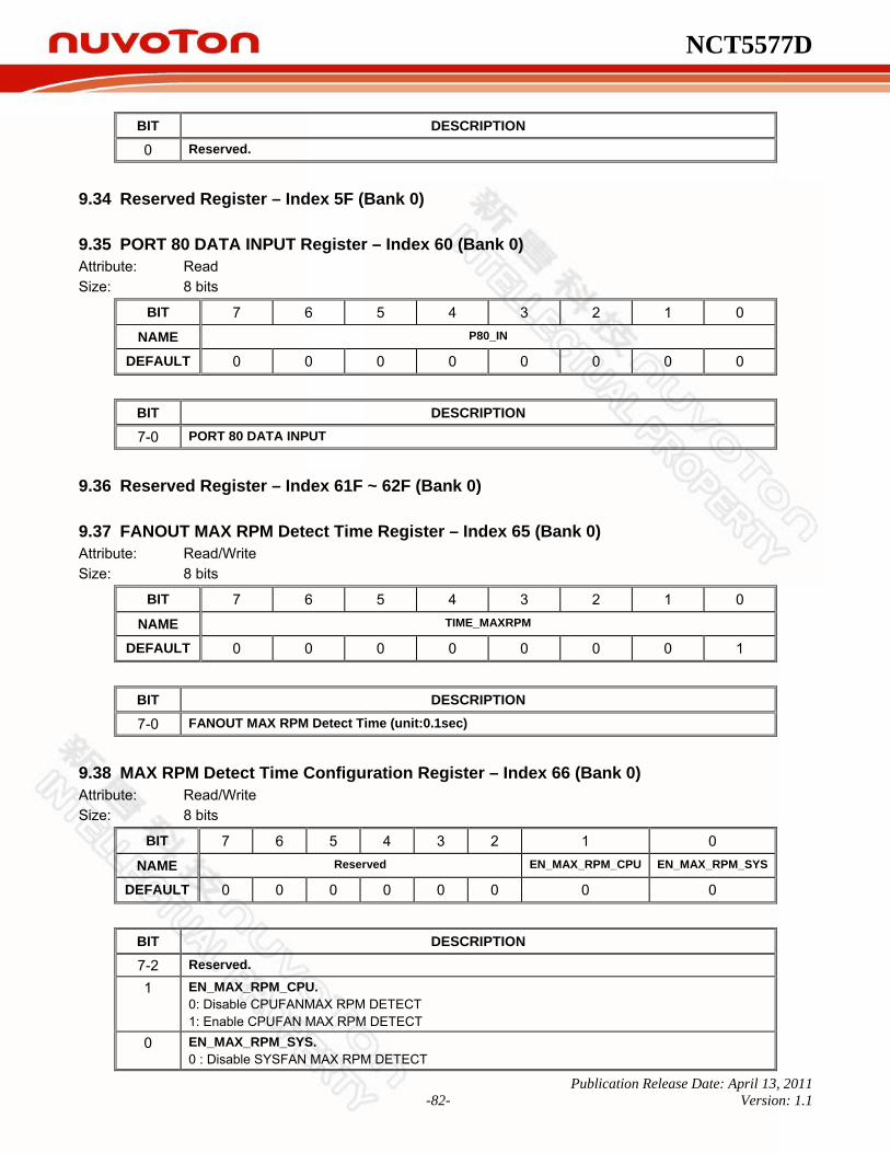
NCT5577D
Publication Release Date: April 13, 2011 -82- Version: 1.1
BIT DESCRIPTION
0 Reserved.
9.34 Reserved Register – Index 5F (Bank 0)
9.35 PORT 80 DATA INPUT Register – Index 60 (Bank 0) Attribute: Read Size: 8 bits
BIT 7 6 5 4 3 2 1 0 NAME P80_IN
DEFAULT 0 0 0 0 0 0 0 0
BIT DESCRIPTION
7-0 PORT 80 DATA INPUT
9.36 Reserved Register – Index 61F ~ 62F (Bank 0)
9.37 FANOUT MAX RPM Detect Time Register – Index 65 (Bank 0) Attribute: Read/Write Size: 8 bits
BIT 7 6 5 4 3 2 1 0
NAME TIME_MAXRPM
DEFAULT 0 0 0 0 0 0 0 1
BIT DESCRIPTION
7-0 FANOUT MAX RPM Detect Time (unit:0.1sec)
9.38 MAX RPM Detect Time Configuration Register – Index 66 (Bank 0) Attribute: Read/Write Size: 8 bits
BIT 7 6 5 4 3 2 1 0
NAME Reserved EN_MAX_RPM_CPU EN_MAX_RPM_SYS
DEFAULT 0 0 0 0 0 0 0 0
BIT DESCRIPTION
7-2 Reserved.
1 EN_MAX_RPM_CPU. 0: Disable CPUFANMAX RPM DETECT 1: Enable CPUFAN MAX RPM DETECT
0 EN_MAX_RPM_SYS. 0 : Disable SYSFAN MAX RPM DETECT

NCT5577D
Publication Release Date: April 13, 2011 -83- Version: 1.1
1: Enable SYSFAN MAX RPM DETECT
9.39 Reserved register – Index 67h ~ 72h (Bank 0)
9.40 MONITOR TEMPERATURE 1 Register (Integer Value)- Index 73h (Bank 0) Attribute: Read/Write Size: 8 bits
BIT 7 6 5 4 3 2 1 0
NAME MONITOR TEMPERATURE 1 [8:1] DEFAULT 0 0 0 0 0 0 0 0
BIT DESCRIPTION
7-0 MONITOR TEMPERATURE 1 [8:1] SYSFANOUT fan control temperature reading. (Source is selected by Bank1, Index00 bit[4:0])
9.41 MONITOR TEMPERATURE 1 Register (Fractional Value)- Index 74h (Bank 0) Attribute: Read/Write Size: 8 bits
BIT 7 6 5 4 3 2 1 0
NAME MONITOR TEMPERATURE
1 [0]
Reserved
DEFAULT 0 0 0 0 0 0 0 0
BIT DESCRIPTION
7 MONITOR TEMPERATURE 1 [0] SYSFANOUT fan control temperature reading. (Source is selected by Bank1, Index00 bit[4:0])
6-0 Reserved
9.42 MONITOR TEMPERATURE 2 Register (Integer Value)- Index 75h (Bank 0) Attribute: Read/Write Size: 8 bits
BIT 7 6 5 4 3 2 1 0 NAME MONITOR TEMPERATURE 2 [8:1]
DEFAULT 0 0 0 0 0 0 0 0
BIT DESCRIPTION
7-0 MONITOR TEMPERATURE 2 [8:1] CPUFANOUT fan control temperature reading. (Source is selected by Bank2, Index00 bit[4:0])

NCT5577D
Publication Release Date: April 13, 2011 -84- Version: 1.1
9.43 MONITOR TEMPERATURE 2 Register (Fractional Value)- Index 76h (Bank 0) Attribute: Read/Write Size: 8 bits
BIT 7 6 5 4 3 2 1 0 NAME MONITOR
TEMPERATURE 2 [0]
Reserved
DEFAULT 0 0 0 0 0 0 0 0
BIT DESCRIPTION
7 MONITOR TEMPERATURE 2 [0] CPUFANOUT fan control temperature reading. (Source is selected by Bank2, Index00 bit[4:0])
6-0 Reserved
9.44 Reserved Register - Index 77h (Bank 0)
9.45 Reserved Register - Index 78h (Bank 0)
9.46 Reserved Register – Index 79h~ADh (Bank 0)
9.47 PECI Temperature Reading Enable for SMIOVT and SMART FAN Control Register – Index AEh (Bank 0)
Attribute: Read/Write Size: 8 bits
BIT 7 6 5 4 3 2 1 0
NAME Reserved EN_PECI1 EN_PECI0DEFAULT 0 0 0 0 0 0 0 0
BIT DESCRIPTION
7-2 Reserved.
1 Enable PECI Agent1 0 Enable PECI Agent0
9.48 BEEP Control Register 1 – Index B2h (Bank0) Attribute: Read/Write Size: 8 bits
BIT 7 6 5 4 3 2 1 0 NAME En3VSB_
BP EnVIN3_
BP EnVIN2_
BP EnVIN1_
BP En3VCC_
BP EnAVCC_
BP EnVIN0_
BP EnCPUVCORE_
BP
DEFAULT 0 0 0 0 0 0 0 0

NCT5577D
Publication Release Date: April 13, 2011 -85- Version: 1.1
BIT DESCRIPTION
7 En3VSB_BP 1 : Enable 3VSB Beep function 0 : Disable 3VSB Beep fuction
6 EnVIN3_BP 1 : Enable VIN3 Beep function 0 : Disable VIN3 Beep fuction
5 EnVIN2_BP 1 : Enable VIN2 Beep function 0 : Disable VIN2 Beep fuction
4 EnVIN1_BP 1 : Enable VIN1 Beep function 0 : Disable VIN1 Beep fuction
3 En3VCC_BP 1 : Enable 3VCC Beep function 0 : Disable 3VCC Beep fuction
2 EnAVCC_BP 1 : Enable AVCC Beep function 0 : Disable AVCC Beep fuction
1 EnVIN0_BP 1 : Enable VIN0 Beep function 0 : Disable VIN0 Beep fuction
0 EnCPUVCORE_BP 1 : Enable CPUVCORE Beep function 0 : Disable CPUVCORE Beep fuction
9.49 BEEP Control Register 2 – Index B3h (Bank0) Attribute: Read/Write Size: 8 bits
BIT 7 6 5 4 3 2 1 0
NAME User Mode
Reserved EnVBAT_BP
DEFAULT 0 0 0 0 0 0 0 0
BIT DESCRIPTION
7 User control for Beep alarm 1 : Enable 0 : Disable
6-1 Reserved 0 EnVBAT_BP
1 : Enable VBAT Beep function 0 : Disable VBAT Beep fuction
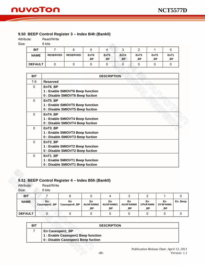
NCT5577D
Publication Release Date: April 13, 2011 -86- Version: 1.1
9.50 BEEP Control Register 3 – Index B4h (Bank0) Attribute: Read/Write Size: 8 bits
BIT 7 6 5 4 3 2 1 0 NAME RESERVED RESERVED EnT6
_BP EnT5 _BP
EnT4 _BP
EnT3 _BP
EnT2 _BP
EnT1 _BP
DEFAULT 0 0 0 0 0 0 0 0
BIT DESCRIPTION
7-6 Reserved 0 EnT6_BP
1 : Enable SMIOVT6 Beep function 0 : Disable SMIOVT6 Beep fuction
0 EnT5_BP 1 : Enable SMIOVT5 Beep function 0 : Disable SMIOVT5 Beep fuction
0 EnT4_BP 1 : Enable SMIOVT4 Beep function 0 : Disable SMIOVT4 Beep fuction
0 EnT3_BP 1 : Enable SMIOVT3 Beep function 0 : Disable SMIOVT3 Beep fuction
0 EnT2_BP 1 : Enable SMIOVT2 Beep function 0 : Disable SMIOVT2 Beep fuction
0 EnT1_BP 1 : Enable SMIOVT1 Beep function 0 : Disable SMIOVT1 Beep fuction
9.51 BEEP Control Register 4 – Index B5h (Bank0) Attribute: Read/Write Size: 8 bits
BIT 7 6 5 4 3 2 1 0
NAME En Caseopen1_BP
En Caseopen0_BP
En AUXFANIN2
_BP
En AUXFANIN1
_BP
En AUXFANIN0
_BP
En CPUFANIN
_BP
En SYSFANIN
_BP
En_Beep
DEFAULT 0 0 0 0 0 0 0 0
BIT DESCRIPTION
7 En Caseopen1_BP 1 : Enable Caseopen1 Beep function 0 : Disable Caseopen1 Beep fuction
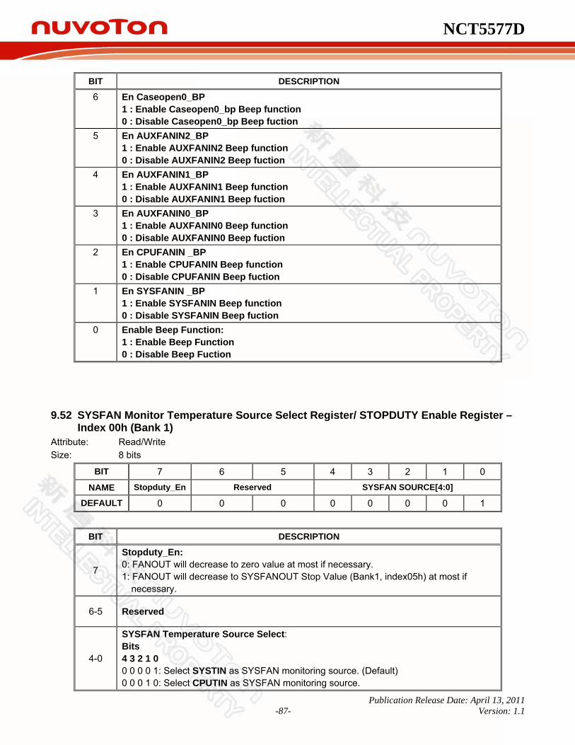
NCT5577D
Publication Release Date: April 13, 2011 -87- Version: 1.1
BIT DESCRIPTION
6 En Caseopen0_BP 1 : Enable Caseopen0_bp Beep function 0 : Disable Caseopen0_bp Beep fuction
5 En AUXFANIN2_BP 1 : Enable AUXFANIN2 Beep function 0 : Disable AUXFANIN2 Beep fuction
4 En AUXFANIN1_BP 1 : Enable AUXFANIN1 Beep function 0 : Disable AUXFANIN1 Beep fuction
3 En AUXFANIN0_BP 1 : Enable AUXFANIN0 Beep function 0 : Disable AUXFANIN0 Beep fuction
2 En CPUFANIN _BP 1 : Enable CPUFANIN Beep function 0 : Disable CPUFANIN Beep fuction
1 En SYSFANIN _BP 1 : Enable SYSFANIN Beep function 0 : Disable SYSFANIN Beep fuction
0 Enable Beep Function: 1 : Enable Beep Function 0 : Disable Beep Fuction
9.52 SYSFAN Monitor Temperature Source Select Register/ STOPDUTY Enable Register – Index 00h (Bank 1)
Attribute: Read/Write Size: 8 bits
BIT 7 6 5 4 3 2 1 0
NAME Stopduty_En Reserved SYSFAN SOURCE[4:0]
DEFAULT 0 0 0 0 0 0 0 1
BIT DESCRIPTION
7
Stopduty_En: 0: FANOUT will decrease to zero value at most if necessary. 1: FANOUT will decrease to SYSFANOUT Stop Value (Bank1, index05h) at most if
necessary.
6-5 Reserved
4-0
SYSFAN Temperature Source Select: Bits 4 3 2 1 0 0 0 0 0 1: Select SYSTIN as SYSFAN monitoring source. (Default) 0 0 0 1 0: Select CPUTIN as SYSFAN monitoring source.

NCT5577D
Publication Release Date: April 13, 2011 -88- Version: 1.1
BIT DESCRIPTION 0 0 0 1 1: Select AUXTIN as SYSFAN monitoring source. 0 0 1 0 0: Select SMBUSMASTER 0 as SYSFAN monitoring source. 0 0 1 0 1: Select SMBUSMASTER 1 as SYSFAN monitoring source. 0 0 1 1 0: Select SMBUSMASTER 2 as SYSFAN monitoring source. 0 0 1 1 1: Select SMBUSMASTER 3 as SYSFAN monitoring source. 0 1 0 0 0: Select SMBUSMASTER 4 as SYSFAN monitoring source. 0 1 0 0 1: Select SMBUSMASTER 5 as SYSFAN monitoring source. 0 1 0 1 0: Select SMBUSMASTER 6 as SYSFAN monitoring source. 0 1 0 1 1: Select SMBUSMASTER 7 as SYSFAN monitoring source. 0 1 1 0 0: Select PECI Agent 0 as SYSFAN monitoring source. 0 1 1 0 1: Select PECI Agent 1 as SYSFAN monitoring source. 0 1 1 1 0: Select PCH_CHIP_CPU_MAX_TEMP as SYSFAN monitoring source. 0 1 1 1 1: Select PCH_CHIP_TEMP as SYSFAN monitoring source. 1 0 0 0 0: Select PCH_CPU_TEMP as SYSFAN monitoring source. 1 0 0 0 1: Select PCH_MCH_TEMP as SYSFAN monitoring source. 1 0 0 1 0: Select PCH_DIM0_TEMP as SYSFAN monitoring source. 1 0 0 1 1: Select PCH_DIM1_TEMP as SYSFAN monitoring source. 1 0 1 0 0: Select PCH_DIM2_TEMP as SYSFAN monitoring source. 1 0 1 0 1: Select PCH_DIM3_TEMP as SYSFAN monitoring source. 1 0 1 1 0: Select BYTE_TEMP as SYSFAN monitoring source.
Note. If the temperature source is selecting to PECI, please set Bank0 Index AEh first for reading correct value
9.53 SYSFAN Target Temperature Register / SYSFANIN Target Speed_L Register – Index 01h (Bank 1)
Attribute: Read/Write Size: 8 bits
BIT 7 6 5 4 3 2 1 0 NAME SYSTIN Target Temperature / SYSFANIN Target Speed_L
DEFAULT 0 0 0 0 0 0 0 0
FUNCTION MODE 7 6 5 4 3 2 1 0
Thermal CruiseTM DESCRIPTION SYSFAN Target Temperature
Fan Speed CruiseTM DESCRIPTION SYSFANIN Target Speed [7:0], associate index 0C [11:8]
9.54 SYSFAN MODE Register / SYSFAN TOLERRANCE Register – Index 02h (Bank 1) Attribute: Read/Write Size: 8 bits
BIT 7 6 5 4 3 2 1 0
NAME SYSFAN MODE Tolerance of SYSFAN Target Temperature or
SYSFANIN Target Speed
DEFAULT 0 0 0 0 Reserved 0 0 0
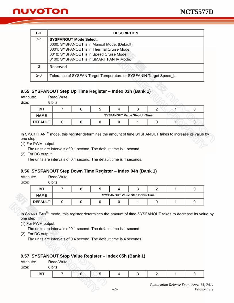
NCT5577D
Publication Release Date: April 13, 2011 -89- Version: 1.1
BIT DESCRIPTION
7-4 SYSFANOUT Mode Select. 0000: SYSFANOUT is in Manual Mode. (Default) 0001: SYSFANOUT is in Thermal Cruise Mode. 0010: SYSFANOUT is in Speed Cruise Mode. 0100: SYSFANOUT is in SMART FAN IV Mode.
3 Reserved
2-0 Tolerance of SYSFAN Target Temperature or SYSFANIN Target Speed_L.
9.55 SYSFANOUT Step Up Time Register – Index 03h (Bank 1) Attribute: Read/Write Size: 8 bits
BIT 7 6 5 4 3 2 1 0
NAME SYSFANOUT Value Step Up Time
DEFAULT 0 0 0 0 1 0 1 0
In SMART FANTM mode, this register determines the amount of time SYSFANOUT takes to increase its value by one step. (1) For PWM output:
The units are intervals of 0.1 second. The default time is 1 second. (2) For DC output:
The units are intervals of 0.4 second. The default time is 4 seconds.
9.56 SYSFANOUT Step Down Time Register – Index 04h (Bank 1) Attribute: Read/Write Size: 8 bits
BIT 7 6 5 4 3 2 1 0
NAME SYSFANOUT Value Step Down Time
DEFAULT 0 0 0 0 1 0 1 0
In SMART FANTM mode, this register determines the amount of time SYSFANOUT takes to decrease its value by one step. (1) For PWM output:
The units are intervals of 0.1 second. The default time is 1 second. (2) For DC output:
The units are intervals of 0.4 second. The default time is 4 seconds.
9.57 SYSFANOUT Stop Value Register – Index 05h (Bank 1) Attribute: Read/Write Size: 8 bits
BIT 7 6 5 4 3 2 1 0

NCT5577D
Publication Release Date: April 13, 2011 -90- Version: 1.1
NAME SYSFANOUT Stop Value
DEFAULT 0 0 0 0 0 0 0 1
In Thermal Cruise mode, the SYSFANOUT value decreases to this eight-bit value if the temperature stays below the lowest temperature limit. This value should not be zero. Please note that Stop Value does not mean that the fan really stops. It means that if the temperature keeps below low temperature limit, then the fan speed keeps on decreasing until reaching a minimum value, and this is Stop Value.
9.58 SYSFANOUT Start-up Value Register – Index 06h (Bank 1) Attribute: Read/Write Size: 8 bits
BIT 7 6 5 4 3 2 1 0 NAME SYSFANOUT Start-Up Value
DEFAULT 0 0 0 0 0 0 0 1
In Thermal Cruise mode, SYSFANOUT value increases from zero to this eight-bit register value to provide a minimum value to turn on the fan.
9.59 SYSFANOUT Stop Time Register – Index 07h (Bank 1) Attribute: Read/Write Size: 8 bits
BIT 7 6 5 4 3 2 1 0 NAME SYSFANOUT Value Step Down Time
DEFAULT 0 0 1 1 1 1 0 0
In SMART FANTM mode, this register determines the amount of time SYSFANOUT takes to decrease its value by one step. (1) For PWM output:
The units are intervals of 0.1 second. The default time is 1 second. (2) For DC output:
The units are intervals of 0.4 second. The default time is 4 seconds.
9.60 Reserved Register – Index 08h (Bank 1)
9.61 SYSFANOUT Output Value Select Register – Index 09h (Bank 1) Attribute: Read/Write Size: 8 bits
BIT 7 6 5 4 3 2 1 0
NAME SYSFANOUT Value
DEFAULT 1 1 1 1 1 1 1 1
FUNCTION MODE 7 6 5 4 3 2 1 0

NCT5577D
Publication Release Date: April 13, 2011 -91- Version: 1.1
PWM Output (Bank0, Index 04h, bit 0 is 0)
DESCRIPTION The PWM duty cycle is equal to this eight-bit value, divided by 255, times 100%. FFh creates a duty cycle of 100%, and 00h creates a duty cycle of 0%.
DC Voltage Output Bank0, Index 04h, bit 0 is 1) DESCRIPTION
SYSFANOUT voltage control. The output voltage is calculated according to this equation.
OUTPUT Voltage = 64
* FANOUTVref
Note. VREF is approx 2.048V.
Reserved
9.62 SYSFANIN Tolerance_H / Target Speed_H Register – Index 0Ch (Bank 1) Attribute: Read/Write Size: 8 bits
BIT 7 6 5 4 3 2 1 0
NAME Reserved SYSFANIN TOL_H SYSFANIN Target Speed_H
DEFAULT 0 0 0
BIT DESCRIPTION
7 Reserved
6-4 SYSFANIN Tolerance_H [5:3] 3-0 SYSFANIN Target Speed_H [11:8]
9.63 Reserved Register – Index 0Dh (Bank 1)
9.64 SMART FAN IV SYSFANOUT STEP Register – Index 20h (Bank 1) Attribute: Read/Write Size: 8 bits
BIT 7 6 5 4 3 2 1 0
NAME Reserved En_SYSFANOUT_STEP
DEFAULT 0 0 0 0 0 0 0 0
BIT DESCRIPTION
7-1 Reserved
0 En_SYSFANOUT_STEP 0: Disable SMART FAN IV has Stepping SYSFANOUT. (default) 1: Enable SMART FAN IV has Stepping SYSFANOUT.
9.65 SYSFAN (SMART FANTM IV) Temperature 1 Register(T1) – Index 21h (Bank 1) Attribute: Read/Write Size: 8 bits

NCT5577D
Publication Release Date: April 13, 2011 -92- Version: 1.1
BIT 7 6 5 4 3 2 1 0 NAME SYSFAN (SMART FANTM IV) Temperature 1
DEFAULT 0 0 0 1 1 0 0 1
BIT DESCRIPTION
7-0 SYSFAN (SMART FANTM IV) Temperature 1 Register (T1).
9.66 SYSFAN (SMART FANTM IV) Temperature 2 Register(T2) – Index 22h (Bank 1) Attribute: Read/Write Size: 8 bits
BIT 7 6 5 4 3 2 1 0
NAME SYSFAN (SMART FANTM IV) Temperature 2
DEFAULT 0 0 1 0 0 1 1 0
BIT DESCRIPTION
7-0 SYSFAN (SMART FANTM IV) Temperature 2 Register (T2).
9.67 SYSFAN (SMART FANTM IV) Temperature 3 Register(T3) – Index 23h (Bank 1) Attribute: Read/Write Size: 8 bits
BIT 7 6 5 4 3 2 1 0 NAME SYSFAN (SMART FANTM IV) Temperature 3
DEFAULT 0 0 1 0 1 1 0 1
BIT DESCRIPTION
7-0 SYSFAN (SMART FANTM IV) Temperature 3 Register (T3).
9.68 SYSFAN (SMART FANTM IV) Temperature 4 Register(T4) – Index 24h (Bank 1) Attribute: Read/Write Size: 8 bits
BIT 7 6 5 4 3 2 1 0
NAME SYSFAN (SMART FANTM IV) Temperature 4
DEFAULT 0 0 1 1 0 1 1 1
BIT DESCRIPTION
7-0 SYSFAN (SMART FANTM IV) Temperature 4 Register (T4).
9.69 SYSFAN (SMART FANTM IV) DC/PWM 1 Register – Index 27h (Bank 1) Attribute: Read/Write

NCT5577D
Publication Release Date: April 13, 2011 -93- Version: 1.1
Size: 8 bits
BIT 7 6 5 4 3 2 1 0
NAME SYSFAN (SMART FANTM IV) DC/PWM 1
DEFAULT 1 0 0 0 1 1 0 0
BIT DESCRIPTION
7-0 SYSFAN (SMART FANTM IV) DC/PWM 1 Register.
9.70 SYSFAN (SMART FANTM IV) DC/PWM 2 Register – Index 28h (Bank 1) Attribute: Read/Write Size: 8 bits
BIT 7 6 5 4 3 2 1 0
NAME SYSFAN (SMART FANTM IV) DC/PWM 2
DEFAULT 1 0 1 0 1 0 1 0
BIT DESCRIPTION
7-0 SYSFAN (SMART FANTM IV) DC/PWM 2 Register.
9.71 SYSFAN (SMART FANTM IV) DC/PWM 3 Register – Index 29h (Bank 1) Attribute: Read/Write Size: 8 bits
BIT 7 6 5 4 3 2 1 0
NAME SYSFAN (SMART FANTM IV) DC/PWM 3
DEFAULT 1 1 0 0 1 0 0 0
BIT DESCRIPTION
7-0 SYSFAN (SMART FANTM IV) DC/PWM 3 Register.
9.72 SYSFAN (SMART FANTM IV) DC/PWM 4 Register – Index 2Ah (Bank 1) Attribute: Read/Write Size: 8 bits
BIT 7 6 5 4 3 2 1 0 NAME SYSFAN (SMART FANTM IV) DC/PWM 4
DEFAULT 1 1 1 0 0 1 1 0
BIT DESCRIPTION
7-0 SYSFAN (SMART FANTM IV) DC/PWM 4 Register.
9.73 Reserved Register – Index 2Bh~30h (Bank 1)

NCT5577D
Publication Release Date: April 13, 2011 -94- Version: 1.1
9.74 SYSFAN 3-Wire Enable Register – Index 31h (Bank 1) Attribute: Read Only Size: 8 bits
BIT 7 6 5 4 3 2 1 0 NAME Reserved EN_SYS_3WFAN
DEFAULT 0 0
BIT DESCRIPTION
7-1 Reserved 0 EN_SYS_3WFAN (SYSFAN type setting)
0: 4-wire fan 1: 3-wire fan
9.75 Reserved Register – Index 32h ~ 34h(Bank 1)
9.76 SYSFAN (SMART FANTM IV) Temperature Critical Register(TR) – Index 35h (Bank 1) Attribute: Read/Write Size: 8 bits
BIT 7 6 5 4 3 2 1 0
NAME SYSFAN (SMART FANTM IV) Temperature Critical
DEFAULT 0 0 1 1 1 1 0 0
BIT DESCRIPTION
7-0 SYSFAN (SMART FANTM IV) Temperature Critical Register (TR).
9.77 Reserved Register – Index 36h ~ 37h (Bank 1)
9.78 SYSFANOUT Critical Temperature Tolerance Register – Index 38h (Bank 1) Attribute: Read/Write Size: 8 bits
BIT 7 6 5 4 3 2 1 0
NAME Reserved SYSFANOUT Critical Temperature Tolerance
DEFAULT 0 0
BIT DESCRIPTION
7-3 Reserved 2-0 SYSFANOUT Critical Temperature Tolerance

NCT5577D
Publication Release Date: April 13, 2011 -95- Version: 1.1
9.79 Weight value Configuration Register – Index 39h (Bank 1) Attribute: Read/Write Size: 8 bits
BIT 7 6 5 4 3 2 1 0 NAME EN_SYSFAN_WEIGHT Reserved SYS_WEIGHT_SEL
DEFAULT 0 0 0 0 0 0 1
BIT DESCRIPTION
7 EN_SYSFAN_WEIGHT. 0: Disable Weight Value Control for SYSFAN. 1: Enable Weight Value Control for SYSFAN.
6-5 Reserved
4-0 SYSFAN Weighting Temperature Source Select: Bits 4 3 2 1 0 0 0 0 0 1: Select SYSTIN as SYSFAN monitoring source. (Default) 0 0 0 1 0: Select CPUTIN as SYSFAN monitoring source. 0 0 0 1 1: Select AUXTIN as SYSFAN monitoring source. 0 0 1 0 0: Select SMBUSMASTER 0 as SYSFAN monitoring source. 0 0 1 0 1: Select SMBUSMASTER 1 as SYSFAN monitoring source. 0 0 1 1 0: Select SMBUSMASTER 2 as SYSFAN monitoring source. 0 0 1 1 1: Select SMBUSMASTER 3 as SYSFAN monitoring source. 0 1 0 0 0: Select SMBUSMASTER 4 as SYSFAN monitoring source. 0 1 0 0 1: Select SMBUSMASTER 5 as SYSFAN monitoring source. 0 1 0 1 0: Select SMBUSMASTER 6 as SYSFAN monitoring source. 0 1 0 1 1: Select SMBUSMASTER 7 as SYSFAN monitoring source. 0 1 1 0 0: Select PECI Agent 0 as SYSFAN monitoring source. 0 1 1 0 1: Select PECI Agent 1 as SYSFAN monitoring source. 0 1 1 1 0: Select PCH_CHIP_CPU_MAX_TEMP as SYSFAN monitoring source. 0 1 1 1 1: Select PCH_CHIP_TEMP as SYSFAN monitoring source. 1 0 0 0 0: Select PCH_CPU_TEMP as SYSFAN monitoring source. 1 0 0 0 1: Select PCH_MCH_TEMP as SYSFAN monitoring source. 1 0 0 1 0: Select PCH_DIM0_TEMP as SYSFAN monitoring source. 1 0 0 1 1: Select PCH_DIM1_TEMP as SYSFAN monitoring source. 1 0 1 0 0: Select PCH_DIM2_TEMP as SYSFAN monitoring source. 1 0 1 0 1: Select PCH_DIM3_TEMP as SYSFAN monitoring source. 1 0 1 1 0: Select BYTE_TEMP as SYSFAN monitoring source.
9.80 SYSFANOUT Temperature Step Register – Index 3Ah (Bank 1) Attribute: Read/Write Size: 8 bits
BIT 7 6 5 4 3 2 1 0
NAME SYSFANOUT Temperature Step (SYS_TEMP_STEP)
DEFAULT 0

NCT5577D
Publication Release Date: April 13, 2011 -96- Version: 1.1
BIT DESCRIPTION
7-0 SYSFANOUT Temperature Step
9.81 SYSFANOUT Temperature Step Tolerance Register – Index 3Bh (Bank 1) Attribute: Read/Write Size: 8 bits
BIT 7 6 5 4 3 2 1 0
NAME SYSFANOUT Temperature Step Tolerance (SYS_TEMP_STEP_TOL)
DEFAULT 0
BIT DESCRIPTION
7-0 SYSFANOUT Temperature Step Tolerance
9.82 SYSFANOUT Weight Step Register – Index 3Ch (Bank 1) Attribute: Read/Write Size: 8 bits
BIT 7 6 5 4 3 2 1 0
NAME SYSFANOUT Weight Step (SYS_WEIGHT_STEP)
DEFAULT 0
BIT DESCRIPTION
7-0 SYSFANOUT Weight Step
9.83 SYSFANOUT Temperature Base Register – Index 3Dh (Bank 1) Attribute: Read/Write Size: 8 bits
BIT 7 6 5 4 3 2 1 0
NAME SYSFANOUT Temperature Base (SYS_TEMP_BASE)
DEFAULT 0
BIT DESCRIPTION
7-0 SYSFANOUT Temperature Base
9.84 SYSFANOUT Temperature Fan Duty Base Register – Index 3Eh (Bank 1) Attribute: Read/Write Size: 8 bits
BIT 7 6 5 4 3 2 1 0

NCT5577D
Publication Release Date: April 13, 2011 -97- Version: 1.1
NAME SYSFANOUT Temperature Base (SYS_FC_BASE)
DEFAULT 0
BIT DESCRIPTION
7-0 SYSFANOUT Start point of Fan Duty increasing
9.85 Reserved Register – Index 3Fh (Bank 1)
9.86 Reserved Register – Index 40h (Bank 1)
9.87 Reserved Register – Index 41h (Bank 1)
9.88 Reserved Register – Index 42h ~ 44h (Bank 1)
9.89 SYSFAN Maximum RPM (Low Byte) Register – Index 45h (Bank 1) Attribute: Read Size: 8 bits
BIT 7 6 5 4 3 2 1 0 NAME MAX_RPM_SYS_LSB
DEFAULT 0 0 0 0 0 0 0 0
BIT DESCRIPTION
7-0 SYSFAN Maximum RPM (Low Byte) register.
9.90 SYSFAN Maximum RPM (High Byte) Register – Index 46h (Bank 1) Attribute: Read Size: 8 bits
BIT 7 6 5 4 3 2 1 0 NAME MAX_RPM_SYS_MSB
DEFAULT 0 0 0 0 0 0 0 0
BIT DESCRIPTION 7-0 SYSFAN Maximum RPM (High Byte) register.
9.91 Reserved Register – Index 49h ~ 4Fh (Bank1)
9.92 SMIOVT2 Temperature Source (High Byte) Register – Index 50h (Bank 1) Attribute: Read Only Size: 8 bits
BIT 7 6 5 4 3 2 1 0

NCT5577D
Publication Release Date: April 13, 2011 -98- Version: 1.1
NAME TEMP<8:1>
BIT DESCRIPTION
7-0 Temperature <8:1> (default: CPUTIN temperature source). The nine-bit value is in units of 0.5℃.
9.93 SMIOVT2 Temperature Source (Low Byte) Register – Index 51h (Bank 1) Attribute: Read Only Size: 8 bits
BIT 7 6 5 4 3 2 1 0
NAME TEMP<0> RESERVED
BIT DESCRIPTION
7 Temperature <0> (default: CPUTIN temperature source). The nine-bit value is in units of 0.5°C.
6-0 Reserved.
9.94 SMIOVT2 Temperature Source Configuration Register – Index 52h (Bank 1) Attribute: Read/Write Size: 8 bits
BIT 7 6 5 4 3 2 1 0
NAME RESERVED FAULT RESERVED OVTMOD STOP
DEFAULT 0 0 0 0 0 0 0 0
BIT DESCRIPTION
7-5 Reserved. This bit should be set to zero.
4-3 Fault. Number of faults to detect before setting OVT# output. This avoids false strapping due to noise.
2 Reserved. This bit should be set to zero.
1 OVTMOD. SMIOVT2 Mode Select. 0 : Compare Mode. (Default) 1: Interrupt Mode.
0 STOP. 0: Monitor SMIOVT2 temperature source. 1: Stop monitoring SMIOVT2 temperature source.
9.95 SMIOVT2 Temperature Source Hysteresis (High Byte) Register – Index 53h (Bank 1) Attribute: Read/Write Size: 8 bits
BIT 7 6 5 4 3 2 1 0 NAME THYST<8:1>
DEFAULT 0 1 0 0 1 0 1 1
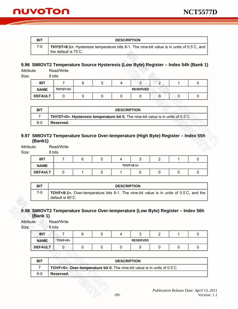
NCT5577D
Publication Release Date: April 13, 2011 -99- Version: 1.1
BIT DESCRIPTION
7-0 THYST<8:1>. Hysteresis temperature bits 8-1. The nine-bit value is in units of 0.5°C, and the default is 75°C.
9.96 SMIOVT2 Temperature Source Hysteresis (Low Byte) Register – Index 54h (Bank 1) Attribute: Read/Write Size: 8 bits
BIT 7 6 5 4 3 2 1 0 NAME THYST<0> RESERVED
DEFAULT 0 0 0 0 0 0 0 0
BIT DESCRIPTION
7 THYST<0>. Hysteresis temperature bit 0. The nine-bit value is in units of 0.5°C. 6-0 Reserved.
9.97 SMIOVT2 Temperature Source Over-temperature (High Byte) Register – Index 55h (Bank1)
Attribute: Read/Write Size: 8 bits
BIT 7 6 5 4 3 2 1 0
NAME TOVF<8:1>
DEFAULT 0 1 0 1 0 0 0 0
BIT DESCRIPTION
7-0 TOVF<8:1>. Over-temperature bits 8-1. The nine-bit value is in units of 0.5°C, and the default is 80°C.
9.98 SMIOVT2 Temperature Source Over-temperature (Low Byte) Register – Index 56h (Bank 1)
Attribute: Read/Write Size: 8 bits
BIT 7 6 5 4 3 2 1 0 NAME TOVF<0> RESERVED
DEFAULT 0 0 0 0 0 0 0 0
BIT DESCRIPTION
7 TOVF<0>. Over-temperature bit 0. The nine-bit value is in units of 0.5°C. 6-0 Reserved.

NCT5577D
Publication Release Date: April 13, 2011 -100- Version: 1.1
9.99 Reserved Register – Index 57h ~ 7Fh (Bank 1)
9.100 CPUFAN Monitor Temperature Source Select Register/ STOPDUTY Enable Register – Index 00h (Bank 2)
Attribute: Read/Write Size: 8 bits
BIT 7 6 5 4 3 2 1 0
NAME Stopduty_En Reserved CPUFAN SOURCE[4:0]
DEFAULT 0 0 0 0 0 0 1 0
BIT DESCRIPTION
7
Stopduty_En: 0: FANOUT will decrease to zero value at most if necessary. 1: FANOUT will decrease to CPUFANOUT Stop Value (Bank2, index05h) at most if
necessary.
6-5 Reserved
4-0
CPUFAN Temperature Source Select: Bits 4 3 2 1 0 0 0 0 0 1: Select SYSTIN as CPUFAN monitoring source. 0 0 0 1 0: Select CPUTIN as CPUFAN monitoring source. (Default) 0 0 0 1 1: Select AUXTIN as CPUFAN monitoring source. 0 0 1 0 0: Select SMBUSMASTER 0 as CPUFAN monitoring source. 0 0 1 0 1: Select SMBUSMASTER 1 as CPUFAN monitoring source. 0 0 1 1 0: Select SMBUSMASTER 2 as CPUFAN monitoring source. 0 0 1 1 1: Select SMBUSMASTER 3 as CPUFAN monitoring source. 0 1 0 0 0: Select SMBUSMASTER 4 as CPUFAN monitoring source. 0 1 0 0 1: Select SMBUSMASTER 5 as CPUFAN monitoring source. 0 1 0 1 0: Select SMBUSMASTER 6 as CPUFAN monitoring source. 0 1 0 1 1: Select SMBUSMASTER 7 as CPUFAN monitoring source. 0 1 1 0 0: Select PECI Agent 0 as CPUFAN monitoring source. 0 1 1 0 1: Select PECI Agent 1 as CPUFAN monitoring source. 0 1 1 1 0: Select PCH_CHIP_CPU_MAX_TEMP as CPUFAN monitoring source. 0 1 1 1 1: Select PCH_CHIP_TEMP as CPUFAN monitoring source. 1 0 0 0 0: Select PCH_CPU_TEMP as CPUFAN monitoring source. 1 0 0 0 1: Select PCH_MCH_TEMP as CPUFAN monitoring source. 1 0 0 1 0: Select PCH_DIM0_TEMP as CPUFAN monitoring source. 1 0 0 1 1: Select PCH_DIM1_TEMP as CPUFAN monitoring source. 1 0 1 0 0: Select PCH_DIM2_TEMP as CPUFAN monitoring source. 1 0 1 0 1: Select PCH_DIM3_TEMP as CPUFAN monitoring source. 1 0 1 1 0: Select BYTE_TEMP as CPUFAN monitoring source.
Note. If the temperature source is selecting to PECI, please set Bank0 Index AEh first for reading correct value.
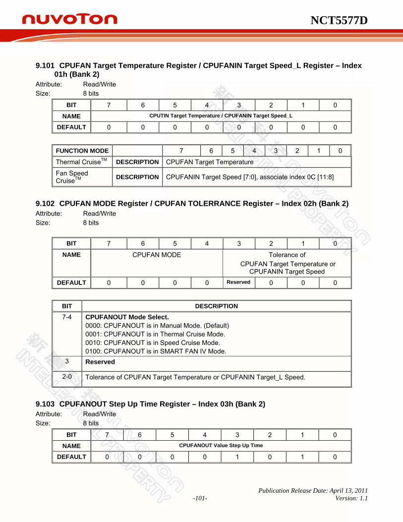
NCT5577D
Publication Release Date: April 13, 2011 -101- Version: 1.1
9.101 CPUFAN Target Temperature Register / CPUFANIN Target Speed_L Register – Index 01h (Bank 2)
Attribute: Read/Write Size: 8 bits
BIT 7 6 5 4 3 2 1 0
NAME CPUTIN Target Temperature / CPUFANIN Target Speed_L
DEFAULT 0 0 0 0 0 0 0 0
FUNCTION MODE 7 6 5 4 3 2 1 0
Thermal CruiseTM DESCRIPTION CPUFAN Target Temperature
Fan Speed CruiseTM DESCRIPTION CPUFANIN Target Speed [7:0], associate index 0C [11:8]
9.102 CPUFAN MODE Register / CPUFAN TOLERRANCE Register – Index 02h (Bank 2) Attribute: Read/Write Size: 8 bits
BIT 7 6 5 4 3 2 1 0
NAME CPUFAN MODE Tolerance of CPUFAN Target Temperature or
CPUFANIN Target Speed
DEFAULT 0 0 0 0 Reserved 0 0 0
BIT DESCRIPTION
7-4 CPUFANOUT Mode Select. 0000: CPUFANOUT is in Manual Mode. (Default) 0001: CPUFANOUT is in Thermal Cruise Mode. 0010: CPUFANOUT is in Speed Cruise Mode. 0100: CPUFANOUT is in SMART FAN IV Mode.
3 Reserved
2-0 Tolerance of CPUFAN Target Temperature or CPUFANIN Target_L Speed.
9.103 CPUFANOUT Step Up Time Register – Index 03h (Bank 2) Attribute: Read/Write Size: 8 bits
BIT 7 6 5 4 3 2 1 0
NAME CPUFANOUT Value Step Up Time
DEFAULT 0 0 0 0 1 0 1 0

NCT5577D
Publication Release Date: April 13, 2011 -102- Version: 1.1
In SMART FANTM mode, this register determines the amount of time CPUFANOUT takes to increase its value by one step. (1) For PWM output:
The units are intervals of 0.1 second. The default time is 1 second. (2) For DC output:
The units are intervals of 0.4 second. The default time is 4 seconds.
9.104 CPUFANOUT Step Down Time Register – Index 04h (Bank 2) Attribute: Read/Write Size: 8 bits
BIT 7 6 5 4 3 2 1 0
NAME CPUFANOUT Value Step Down Time
DEFAULT 0 0 0 0 1 0 1 0
In SMART FANTM mode, this register determines the amount of time CPUFANOUT takes to decrease its value by one step. (1) For PWM output:
The units are intervals of 0.1 second. The default time is 1 second. (2) For DC output:
The units are intervals of 0.4 second. The default time is 4 seconds.
9.105 CPUFANOUT Stop Value Register – Index 05h (Bank 2) Attribute: Read/Write Size: 8 bits
BIT 7 6 5 4 3 2 1 0
NAME CPUFANOUT Stop Value
DEFAULT 0 0 0 0 0 0 0 1
In Thermal Cruise mode, the CPUFANOUT value decreases to this eight-bit value if the temperature stays below the lowest temperature limit. This value should not be zero. Please note that Stop Value does not mean that the fan really stops. It means that if the temperature keeps below low temperature limit, then the fan speed keeps on decreasing until reaching a minimum value, and this is Stop Value.
9.106 CPUFANOUT Start-up Value Register – Index 06h (Bank 2) Attribute: Read/Write Size: 8 bits
BIT 7 6 5 4 3 2 1 0
NAME CPUFANOUT Start-Up Value
DEFAULT 0 0 0 0 0 0 0 1
In Thermal Cruise mode, CPUFANOUT value increases from zero to this eight-bit register value to provide a minimum value to turn on the fan.

NCT5577D
Publication Release Date: April 13, 2011 -103- Version: 1.1
9.107 CPUFANOUT Stop Time Register – Index 07h (Bank 2) Attribute: Read/Write Size: 8 bits
BIT 7 6 5 4 3 2 1 0 NAME CPUFANOUT Value Step Down Time
DEFAULT 0 0 1 1 1 1 0 0
In SMART FANTM mode, this register determines the amount of time CPUFANOUT takes to decrease its value by one step. (1) For PWM output:
The units are intervals of 0.1 second. The default time is 1 second. (2) For DC output:
The units are intervals of 0.4 second. The default time is 4 seconds.
9.108 Reserved Register – Index 08h (Bank 2)
9.109 CPUFANOUT Output Value Select Register – Index 09h (Bank 2) Attribute: Read/Write Size: 8 bits
BIT 7 6 5 4 3 2 1 0
NAME CPUFANOUT Value
DEFAULT Depends on strapping pin – Pin.34 FAN_SET
FUNCTION MODE 7 6 5 4 3 2 1 0 PWM Output (Bank0, Index 04h, bit 0 is 0)
DESCRIPTION The PWM duty cycle is equal to this eight-bit value, divided by 255, times 100%. FFh creates a duty cycle of 100%, and 00h creates a duty cycle of 0%.
DC Voltage Output Bank0, Index 04h, bit 0 is 1) DESCRIPTION
CPUFANOUT voltage control. The output voltage is calculated according to this equation.
OUTPUT Voltage = 64
* FANOUTVref
Note. VREF is approx 2.048V.
Reserved
9.110 CPUFANIN Tolerance_H / Target Speed_H Register – Index 0Ch (Bank 2) Attribute: Read/Write Size: 8 bits
BIT 7 6 5 4 3 2 1 0
NAME Reserved CPUFANIN TOL_H CPUFANIN Target Speed_H
DEFAULT 0 0 0
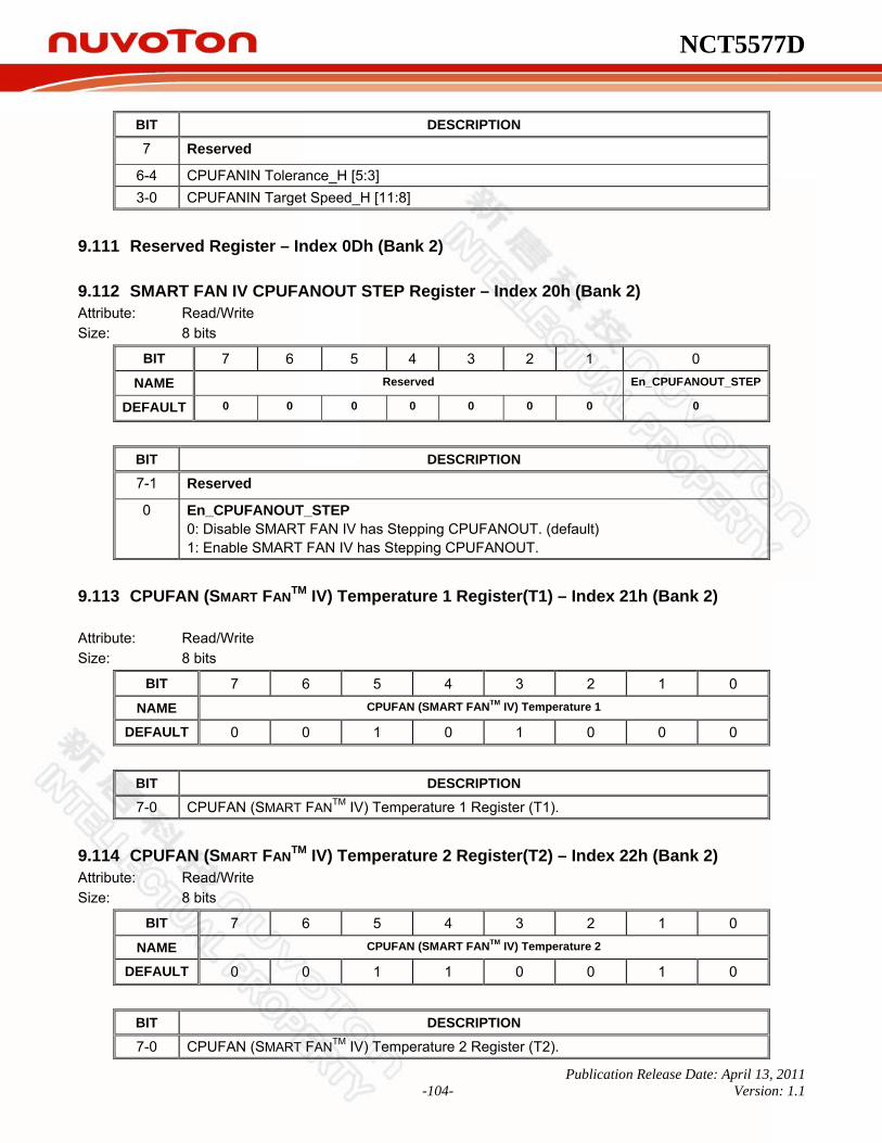
NCT5577D
Publication Release Date: April 13, 2011 -104- Version: 1.1
BIT DESCRIPTION
7 Reserved
6-4 CPUFANIN Tolerance_H [5:3] 3-0 CPUFANIN Target Speed_H [11:8]
9.111 Reserved Register – Index 0Dh (Bank 2)
9.112 SMART FAN IV CPUFANOUT STEP Register – Index 20h (Bank 2) Attribute: Read/Write Size: 8 bits
BIT 7 6 5 4 3 2 1 0 NAME Reserved En_CPUFANOUT_STEP
DEFAULT 0 0 0 0 0 0 0 0
BIT DESCRIPTION
7-1 Reserved
0 En_CPUFANOUT_STEP 0: Disable SMART FAN IV has Stepping CPUFANOUT. (default) 1: Enable SMART FAN IV has Stepping CPUFANOUT.
9.113 CPUFAN (SMART FANTM IV) Temperature 1 Register(T1) – Index 21h (Bank 2) Attribute: Read/Write Size: 8 bits
BIT 7 6 5 4 3 2 1 0 NAME CPUFAN (SMART FANTM IV) Temperature 1
DEFAULT 0 0 1 0 1 0 0 0
BIT DESCRIPTION
7-0 CPUFAN (SMART FANTM IV) Temperature 1 Register (T1).
9.114 CPUFAN (SMART FANTM IV) Temperature 2 Register(T2) – Index 22h (Bank 2) Attribute: Read/Write Size: 8 bits
BIT 7 6 5 4 3 2 1 0
NAME CPUFAN (SMART FANTM IV) Temperature 2
DEFAULT 0 0 1 1 0 0 1 0
BIT DESCRIPTION
7-0 CPUFAN (SMART FANTM IV) Temperature 2 Register (T2).
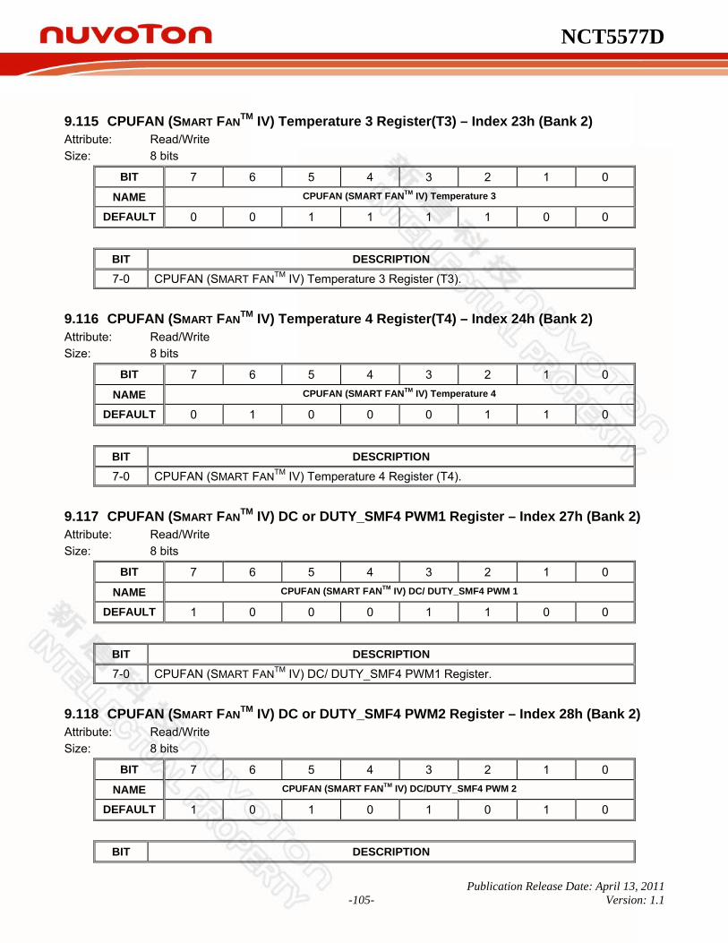
NCT5577D
Publication Release Date: April 13, 2011 -105- Version: 1.1
9.115 CPUFAN (SMART FANTM IV) Temperature 3 Register(T3) – Index 23h (Bank 2) Attribute: Read/Write Size: 8 bits
BIT 7 6 5 4 3 2 1 0 NAME CPUFAN (SMART FANTM IV) Temperature 3
DEFAULT 0 0 1 1 1 1 0 0
BIT DESCRIPTION
7-0 CPUFAN (SMART FANTM IV) Temperature 3 Register (T3).
9.116 CPUFAN (SMART FANTM IV) Temperature 4 Register(T4) – Index 24h (Bank 2) Attribute: Read/Write Size: 8 bits
BIT 7 6 5 4 3 2 1 0
NAME CPUFAN (SMART FANTM IV) Temperature 4
DEFAULT 0 1 0 0 0 1 1 0
BIT DESCRIPTION
7-0 CPUFAN (SMART FANTM IV) Temperature 4 Register (T4).
9.117 CPUFAN (SMART FANTM IV) DC or DUTY_SMF4 PWM1 Register – Index 27h (Bank 2) Attribute: Read/Write Size: 8 bits
BIT 7 6 5 4 3 2 1 0
NAME CPUFAN (SMART FANTM IV) DC/ DUTY_SMF4 PWM 1
DEFAULT 1 0 0 0 1 1 0 0
BIT DESCRIPTION
7-0 CPUFAN (SMART FANTM IV) DC/ DUTY_SMF4 PWM1 Register.
9.118 CPUFAN (SMART FANTM IV) DC or DUTY_SMF4 PWM2 Register – Index 28h (Bank 2) Attribute: Read/Write Size: 8 bits
BIT 7 6 5 4 3 2 1 0 NAME CPUFAN (SMART FANTM IV) DC/DUTY_SMF4 PWM 2
DEFAULT 1 0 1 0 1 0 1 0
BIT DESCRIPTION

NCT5577D
Publication Release Date: April 13, 2011 -106- Version: 1.1
7-0 CPUFAN (SMART FANTM IV) DC/DUTY_SMF4 PWM2 Register.
9.119 CPUFAN (SMART FANTM IV) DC or DUTY_SMF4 PWM3 Register – Index 29h (Bank 2) Attribute: Read/Write Size: 8 bits
BIT 7 6 5 4 3 2 1 0
NAME CPUFAN (SMART FANTM IV) DC/ DUTY_SMF4 PWM 3
DEFAULT 1 1 0 0 1 0 0 0
BIT DESCRIPTION
7-0 CPUFAN (SMART FANTM IV) DC/DUTY_SMF4 PWM3 Register.
9.120 CPUFAN (SMART FANTM IV) DC or DUTY_SMF4 PWM4 Register – Index 2Ah (Bank 2) Attribute: Read/Write Size: 8 bits
BIT 7 6 5 4 3 2 1 0 NAME CPUFAN (SMART FANTM IV) DC/ DUTY_SMF4 PWM4
DEFAULT 1 1 1 0 0 1 1 0
BIT DESCRIPTION
7-0 CPUFAN (SMART FANTM IV) DC/DUTY_SMF4 PWM4 Register.
9.121 Reserved Register – Index 2Dh~ 30h (Bank 2)
9.122 CPUFAN 3-Wire FAN Enable Register – Index 31h (Bank 2) Attribute: Read Only Size: 8 bits
BIT 7 6 5 4 3 2 1 0
NAME Reserved EN_CPU_3WFAN
DEFAULT 0 0
BIT DESCRIPTION
7-1 Reserved
0 EN_CPU_3WFAN (CPUFAN type setting) 0: 4-wire fan 1: 3-wire fan
9.123 Reserved Register – Index 32h ~ 34h(Bank 2)
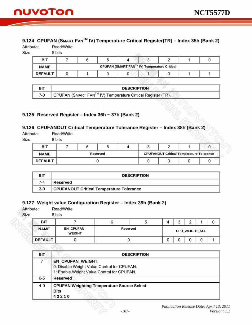
NCT5577D
Publication Release Date: April 13, 2011 -107- Version: 1.1
9.124 CPUFAN (SMART FANTM IV) Temperature Critical Register(TR) – Index 35h (Bank 2) Attribute: Read/Write Size: 8 bits
BIT 7 6 5 4 3 2 1 0 NAME CPUFAN (SMART FANTM IV) Temperature Critical
DEFAULT 0 1 0 0 1 0 1 1
BIT DESCRIPTION
7-0 CPUFAN (SMART FANTM IV) Temperature Critical Register (TR).
9.125 Reserved Register – Index 36h ~ 37h (Bank 2)
9.126 CPUFANOUT Critical Temperature Tolerance Register – Index 38h (Bank 2) Attribute: Read/Write Size: 8 bits
BIT 7 6 5 4 3 2 1 0
NAME Reserved CPUFANOUT Critical Temperature Tolerance
DEFAULT 0 0 0 0 0
BIT DESCRIPTION
7-4 Reserved 3-0 CPUFANOUT Critical Temperature Tolerance
9.127 Weight value Configuration Register – Index 39h (Bank 2) Attribute: Read/Write Size: 8 bits
BIT 7 6 5 4 3 2 1 0 NAME EN_CPUFAN_
WEIGHT Reserved
CPU_WEIGHT_SEL
DEFAULT 0 0 0 0 0 0 1
BIT DESCRIPTION
7 EN_CPUFAN_WEIGHT. 0: Disable Weight Value Control for CPUFAN. 1: Enable Weight Value Control for CPUFAN.
6-5 Reserved
4-0 CPUFAN Weighting Temperature Source Select: Bits 4 3 2 1 0

NCT5577D
Publication Release Date: April 13, 2011 -108- Version: 1.1
BIT DESCRIPTION 0 0 0 0 1: Select SYSTIN as CPUFAN monitoring source. (Default) 0 0 0 1 0: Select CPUTIN as CPUFAN monitoring source. 0 0 0 1 1: Select AUXTIN as CPUFAN monitoring source. 0 0 1 0 0: Select SMBUSMASTER as CPUFAN monitoring source. 0 0 1 0 0: Select SMBUSMASTER 0 as CPUFAN monitoring source. 0 0 1 0 1: Select SMBUSMASTER 1 as CPUFAN monitoring source. 0 0 1 1 0: Select SMBUSMASTER 2 as CPUFAN monitoring source. 0 0 1 1 1: Select SMBUSMASTER 3 as CPUFAN monitoring source. 0 1 0 0 0: Select SMBUSMASTER 4 as CPUFAN monitoring source. 0 1 0 0 1: Select SMBUSMASTER 5 as CPUFAN monitoring source. 0 1 0 1 0: Select SMBUSMASTER 6 as CPUFAN monitoring source. 0 1 0 1 1: Select SMBUSMASTER 7 as CPUFAN monitoring source. 0 1 1 0 0: Select PECI Agent 0 as CPUFAN monitoring source. 0 1 1 0 1: Select PECI Agent 1 as CPUFAN monitoring source. 0 1 1 1 0: Select PCH_CHIP_CPU_MAX_TEMP as CPUFAN monitoring source. 0 1 1 1 1: Select PCH_CHIP_TEMP as CPUFAN monitoring source. 1 0 0 0 0: Select PCH_CPU_TEMP as CPUFAN monitoring source. 1 0 0 0 1: Select PCH_MCH_TEMP as CPUFAN monitoring source. 1 0 0 1 0: Select PCH_DIM0_TEMP as CPUFAN monitoring source. 1 0 0 1 1: Select PCH_DIM1_TEMP as CPUFAN monitoring source. 1 0 1 0 0: Select PCH_DIM2_TEMP as CPUFAN monitoring source. 1 0 1 0 1: Select PCH_DIM3_TEMP as CPUFAN monitoring source. 1 0 1 1 0: Select BYTE_TEMP as CPUFAN monitoring source.
9.128 CPUFANOUT Temperature Step Register – Index 3Ah (Bank 2) Attribute: Read/Write Size: 8 bits
BIT 7 6 5 4 3 2 1 0
BIT CPUFANOUT Temperature Step (CPU_TEMP_STEP)
DEFAULT 0
BIT DESCRIPTION
7-0 CPUFANOUT Temperature Step
9.129 CPUFANOUT Temperature Step Tolerance Register – Index 3Bh (Bank 2) Attribute: Read/Write Size: 8 bits
BIT 7 6 5 4 3 2 1 0
BIT CPUFANOUT Temperature Step Tolerance (CPU_TEMP_STEP_TOL)
DEFAULT 0
BIT DESCRIPTION
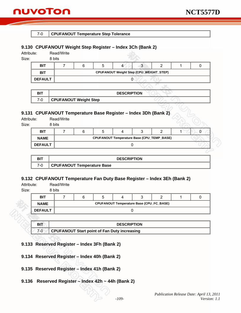
NCT5577D
Publication Release Date: April 13, 2011 -109- Version: 1.1
7-0 CPUFANOUT Temperature Step Tolerance
9.130 CPUFANOUT Weight Step Register – Index 3Ch (Bank 2) Attribute: Read/Write Size: 8 bits
BIT 7 6 5 4 3 2 1 0
BIT CPUFANOUT Weight Step (CPU_WEIGHT_STEP)
DEFAULT 0
BIT DESCRIPTION
7-0 CPUFANOUT Weight Step
9.131 CPUFANOUT Temperature Base Register – Index 3Dh (Bank 2) Attribute: Read/Write Size: 8 bits
BIT 7 6 5 4 3 2 1 0
NAME CPUFANOUT Temperature Base (CPU_TEMP_BASE)
DEFAULT 0
BIT DESCRIPTION
7-0 CPUFANOUT Temperature Base
9.132 CPUFANOUT Temperature Fan Duty Base Register – Index 3Eh (Bank 2) Attribute: Read/Write Size: 8 bits
BIT 7 6 5 4 3 2 1 0 NAME CPUFANOUT Temperature Base (CPU_FC_BASE)
DEFAULT 0
BIT DESCRIPTION
7-0 CPUFANOUT Start point of Fan Duty increasing
9.133 Reserved Register – Index 3Fh (Bank 2)
9.134 Reserved Register – Index 40h (Bank 2)
9.135 Reserved Register – Index 41h (Bank 2)
9.136 Reserved Register – Index 42h ~ 44h (Bank 2)
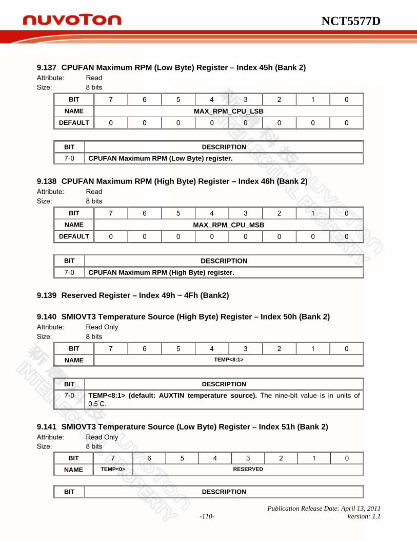
NCT5577D
Publication Release Date: April 13, 2011 -110- Version: 1.1
9.137 CPUFAN Maximum RPM (Low Byte) Register – Index 45h (Bank 2) Attribute: Read Size: 8 bits
BIT 7 6 5 4 3 2 1 0 NAME MAX_RPM_CPU_LSB
DEFAULT 0 0 0 0 0 0 0 0
BIT DESCRIPTION
7-0 CPUFAN Maximum RPM (Low Byte) register.
9.138 CPUFAN Maximum RPM (High Byte) Register – Index 46h (Bank 2) Attribute: Read Size: 8 bits
BIT 7 6 5 4 3 2 1 0 NAME MAX_RPM_CPU_MSB
DEFAULT 0 0 0 0 0 0 0 0
BIT DESCRIPTION 7-0 CPUFAN Maximum RPM (High Byte) register.
9.139 Reserved Register – Index 49h ~ 4Fh (Bank2)
9.140 SMIOVT3 Temperature Source (High Byte) Register – Index 50h (Bank 2) Attribute: Read Only Size: 8 bits
BIT 7 6 5 4 3 2 1 0 NAME TEMP<8:1>
BIT DESCRIPTION
7-0 TEMP<8:1> (default: AUXTIN temperature source). The nine-bit value is in units of 0.5°C.
9.141 SMIOVT3 Temperature Source (Low Byte) Register – Index 51h (Bank 2) Attribute: Read Only Size: 8 bits
BIT 7 6 5 4 3 2 1 0 NAME TEMP<0> RESERVED
BIT DESCRIPTION

NCT5577D
Publication Release Date: April 13, 2011 -111- Version: 1.1
BIT DESCRIPTION
7 Temperature <0> (default: AUXTIN temperature source). The nine-bit value is in units of 0.5°C.
6-0 Reserved.
9.142 SMIOVT3 Temperature Source Configuration Register – Index 52h (Bank 2) Attribute: Read/Write Size: 8 bits
BIT 7 6 5 4 3 2 1 0
NAME RESERVED FAULT RESERVED OVTMOD STOP
DEFAULT 0 0 0 0 0 0 0 0
BIT DESCRIPTION
7-5 Reserved. This bit should be set to zero.
4-3 Fault. Number of faults to detect before setting OVT# output. This avoids false strapping due to noise.
2 Reserved. This bit should be set to zero.
1 OVTMOD. SMIOVT3 Mode Select. 0: Compare Mode. (Default) 1: Interrupt Mode.
0 STOP. 0: Monitor SMIOVT3 temperature source. 1: Stop monitoring SMIOVT3 temperature source.
9.143 SMIOVT3 Temperature Source Hysteresis (High Byte) Register – Index 53h (Bank 2) Attribute: Read/Write Size: 8 bits
BIT 7 6 5 4 3 2 1 0 NAME THYST<8:1>
DEFAULT 0 1 0 0 1 0 1 1
BIT DESCRIPTION
7-0 THYST<8:1>. Hysteresis temperature bits 8-1. The nine-bit value is in units of 0.5°C, and the default is 75°C.
9.144 SMIOVT3 Temperature Source Hysteresis (Low Byte) Register – Index 54h (Bank 2) Attribute: Read/Write Size: 8 bits
BIT 7 6 5 4 3 2 1 0
NAME THYST<0> RESERVED
DEFAULT 0 0 0 0 0 0 0 0
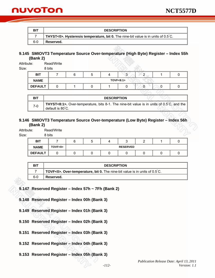
NCT5577D
Publication Release Date: April 13, 2011 -112- Version: 1.1
BIT DESCRIPTION
7 THYST<0>. Hysteresis temperature, bit 0. The nine-bit value is in units of 0.5°C. 6-0 Reserved.
9.145 SMIOVT3 Temperature Source Over-temperature (High Byte) Register – Index 55h (Bank 2)
Attribute: Read/Write Size: 8 bits
BIT 7 6 5 4 3 2 1 0
NAME TOVF<8:1>
DEFAULT 0 1 0 1 0 0 0 0
BIT DESCRIPTION
7-0 THYST<8:1>. Over-temperature, bits 8-1. The nine-bit value is in units of 0.5°C, and the default is 80°C.
9.146 SMIOVT3 Temperature Source Over-temperature (Low Byte) Register – Index 56h (Bank 2)
Attribute: Read/Write Size: 8 bits
BIT 7 6 5 4 3 2 1 0 NAME TOVF<0> RESERVED
DEFAULT 0 0 0 0 0 0 0 0
BIT DESCRIPTION
7 TOVF<0>. Over-temperature, bit 0. The nine-bit value is in units of 0.5°C. 6-0 Reserved.
9.147 Reserved Register – Index 57h ~ 7Fh (Bank 2)
9.148 Reserved Register – Index 00h (Bank 3)
9.149 Reserved Register – Index 01h (Bank 3)
9.150 Reserved Register – Index 02h (Bank 3)
9.151 Reserved Register – Index 03h (Bank 3)
9.152 Reserved Register – Index 04h (Bank 3)
9.153 Reserved Register – Index 05h (Bank 3)
NCT5577D
Publication Release Date: April 13, 2011 -113- Version: 1.1
9.154 Reserved Register – Index 06h (Bank 3)
9.155 Reserved Register – Index 07h (Bank 3)
9.156 Reserved Register – Index 08h (Bank 3)
9.157 Reserved Register – Index 09h (Bank 3)
9.158 Reserved Register – Index 0Ch (Bank 3)
9.159 Reserved Register – Index 0Dh (Bank 3)
9.160 Reserved Register – Index 20h (Bank 3)
9.161 Reserved Register – Index 21h (Bank 3)
9.162 Reserved Register – Index 22h (Bank 3)
9.163 Reserved Register – Index 23h (Bank 3)
9.164 Reserved Register – Index 24h (Bank 3)
9.165 Reserved Register – Index 27h (Bank 3)
9.166 Reserved Register – Index 28h (Bank 3)
9.167 Reserved Register – Index 29h (Bank 3)
9.168 Reserved Register – Index 2Ah (Bank 3)
9.169 Reserved Register – Index Index 2Dh~ 30h (Bank 3)
9.170 Reserved Register – Index 31h (Bank 3)
9.171 Reserved Register – Index 32h ~ 34h(Bank 3)
9.172 Reserved Register – Index 35h (Bank 3)
9.173 Reserved Register – Index 36h ~ 37h (Bank 3)
9.174 Reserved Register – Index 38h (Bank 3)

NCT5577D
Publication Release Date: April 13, 2011 -114- Version: 1.1
9.175 Reserved Register – Index 39h (Bank 3)
9.176 Reserved Register – Index 3Ah (Bank 3)
9.177 Reserved Register – Index 3Bh (Bank 3)
9.178 Reserved Register – Index 3Ch (Bank 3)
9.179 Reserved Register – Index 3Dh (Bank 3)
9.180 Reserved Register – Index 3Eh (Bank 3)
9.181 Reserved Register – Index 3Fh (Bank 3)
9.182 Reserved Register – Index 40h (Bank 3)
9.183 Reserved Register – Index 41h (Bank 3)
9.184 Reserved Register – Index 42h ~ 44h (Bank 3)
9.185 Reserved Register – Index 45h (Bank 3)
9.186 Reserved Register – Index 46h (Bank 3)
9.187 Reserved Register – Index 49h ~ 7Fh (Bank3)
9.188 PCH_CHIP_CPU_MAX_TEMP Register – Index 00h (Bank 4) Attribute: Read Size: 8 bits
BIT 7 6 5 4 3 2 1 0 NAME PCH_CHIP_CPU_MAX_TEMP
DEFAULT 0 0 0 0 0 0 0 0
BIT DESCRIPTION
7-0 PCH_CHIP_CPU_MAX_TEMP: The maximum temperature in absolute degree C, of the CPU and MCH.
9.189 PCH_CHIP_TEMP Register – Index 01h (Bank 4) Attribute: Read Size: 8 bits
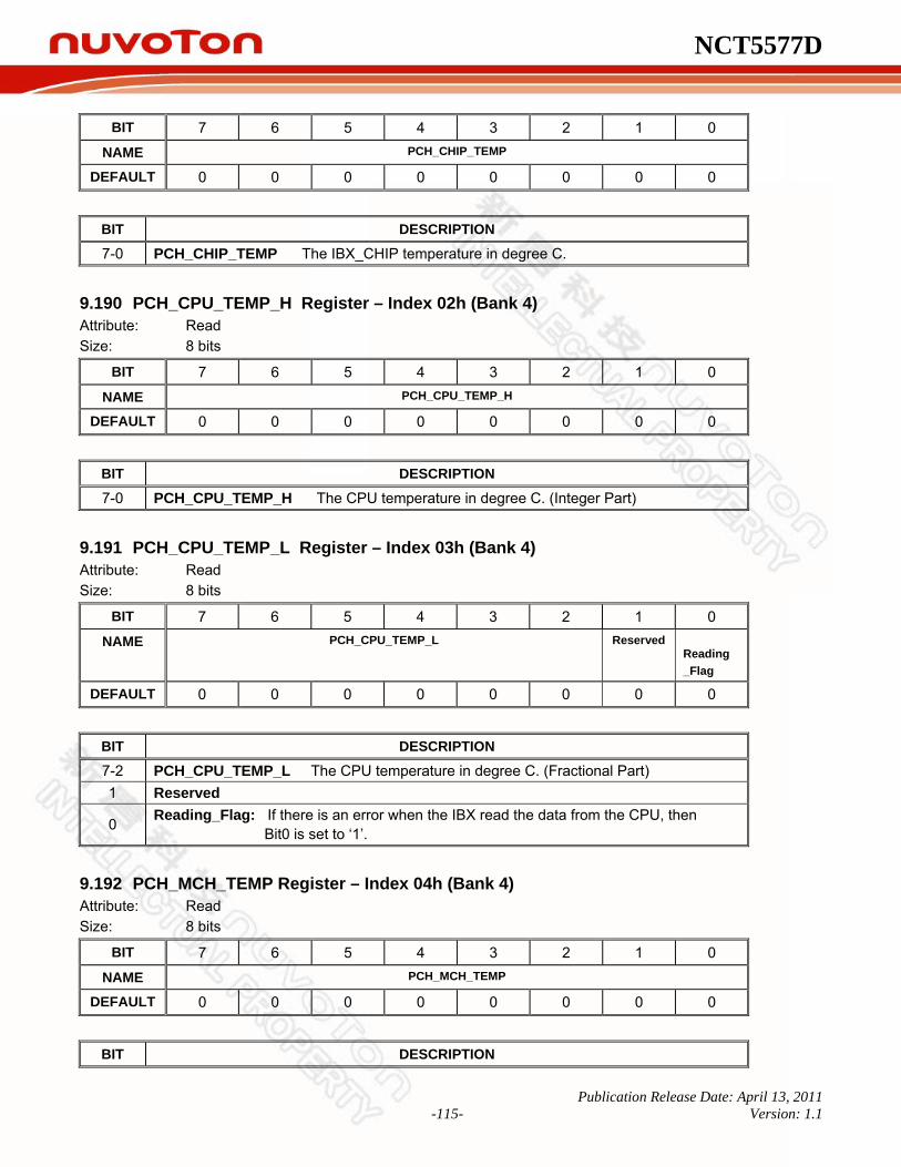
NCT5577D
Publication Release Date: April 13, 2011 -115- Version: 1.1
BIT 7 6 5 4 3 2 1 0 NAME PCH_CHIP_TEMP
DEFAULT 0 0 0 0 0 0 0 0
BIT DESCRIPTION
7-0 PCH_CHIP_TEMP The IBX_CHIP temperature in degree C.
9.190 PCH_CPU_TEMP_H Register – Index 02h (Bank 4) Attribute: Read Size: 8 bits
BIT 7 6 5 4 3 2 1 0
NAME PCH_CPU_TEMP_H
DEFAULT 0 0 0 0 0 0 0 0
BIT DESCRIPTION
7-0 PCH_CPU_TEMP_H The CPU temperature in degree C. (Integer Part)
9.191 PCH_CPU_TEMP_L Register – Index 03h (Bank 4) Attribute: Read Size: 8 bits
BIT 7 6 5 4 3 2 1 0 NAME PCH_CPU_TEMP_L Reserved
Reading _Flag
DEFAULT 0 0 0 0 0 0 0 0
BIT DESCRIPTION
7-2 PCH_CPU_TEMP_L The CPU temperature in degree C. (Fractional Part) 1 Reserved
0 Reading_Flag: If there is an error when the IBX read the data from the CPU, then Bit0 is set to ‘1’.
9.192 PCH_MCH_TEMP Register – Index 04h (Bank 4) Attribute: Read Size: 8 bits
BIT 7 6 5 4 3 2 1 0 NAME PCH_MCH_TEMP
DEFAULT 0 0 0 0 0 0 0 0
BIT DESCRIPTION

NCT5577D
Publication Release Date: April 13, 2011 -116- Version: 1.1
BIT DESCRIPTION
7-0 PCH_MCH_TEMP The MCH temperature in degree C.
9.193 PCH_DIM0_TEMP Register – Index 05h (Bank 4) Attribute: Read Size: 8 bits
BIT 7 6 5 4 3 2 1 0
NAME PCH_DIM0_TEMP
DEFAULT 0 0 0 0 0 0 0 0
BIT DESCRIPTION
7-0 PCH_DIM0_TEMP The DIM0 temperature in degree C.
9.194 PCH_DIM1_TEMP Register – Index 06h (Bank 4) Attribute: Read Size: 8 bits
BIT 7 6 5 4 3 2 1 0 NAME PCH_DIM1_TEMP
DEFAULT 0 0 0 0 0 0 0 0
BIT DESCRIPTION
7-0 PCH_DIM1_TEMP The DIM1 temperature in degree C.
9.195 PCH_DIM2_TEMP Register – Index 07h (Bank 4) Attribute: Read Size: 8 bits
BIT 7 6 5 4 3 2 1 0
NAME PCH_DIM2_TEMP
DEFAULT 0 0 0 0 0 0 0 0
BIT DESCRIPTION
7-0 PCH_DIM2_TEMP The DIM2 temperature in degree C.
9.196 PCH_DIM3_TEMP Register – Index 08h (Bank 4) Attribute: Read Size: 8 bits
BIT 7 6 5 4 3 2 1 0
NAME PCH_DIM3_TEMP
DEFAULT 0 0 0 0 0 0 0 0
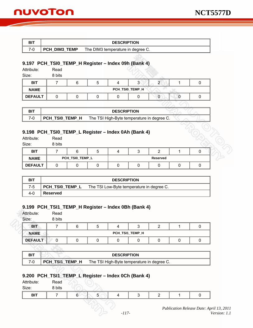
NCT5577D
Publication Release Date: April 13, 2011 -117- Version: 1.1
BIT DESCRIPTION
7-0 PCH_DIM3_TEMP The DIM3 temperature in degree C.
9.197 PCH_TSI0_TEMP_H Register – Index 09h (Bank 4) Attribute: Read Size: 8 bits
BIT 7 6 5 4 3 2 1 0
NAME PCH_TSI0_TEMP_H
DEFAULT 0 0 0 0 0 0 0 0
BIT DESCRIPTION
7-0 PCH_TSI0_TEMP_H The TSI High-Byte temperature in degree C.
9.198 PCH_TSI0_TEMP_L Register – Index 0Ah (Bank 4) Attribute: Read Size: 8 bits
BIT 7 6 5 4 3 2 1 0
NAME PCH_TSI0_TEMP_L Reserved
DEFAULT 0 0 0 0 0 0 0 0
BIT DESCRIPTION
7-5 PCH_TSI0_TEMP_L The TSI Low-Byte temperature in degree C. 4-0 Reserved
9.199 PCH_TSI1_TEMP_H Register – Index 0Bh (Bank 4) Attribute: Read Size: 8 bits
BIT 7 6 5 4 3 2 1 0
NAME PCH_TSI1_TEMP_H
DEFAULT 0 0 0 0 0 0 0 0
BIT DESCRIPTION
7-0 PCH_TSI1_TEMP_H The TSI High-Byte temperature in degree C.
9.200 PCH_TSI1_TEMP_L Register – Index 0Ch (Bank 4) Attribute: Read Size: 8 bits
BIT 7 6 5 4 3 2 1 0

NCT5577D
Publication Release Date: April 13, 2011 -118- Version: 1.1
NAME PCH_TSI1_TEMP_L Reserved
DEFAULT 0 0 0 0 0 0 0 0
BIT DESCRIPTION
7-5 PCH_TSI1_TEMP_L The TSI Low-Byte temperature in degree C. 4-0 Reserved
9.201 PCH_TSI2_TEMP_H Register – Index 0Dh (Bank 4) Attribute: Read Size: 8 bits
BIT 7 6 5 4 3 2 1 0
NAME PCH_TSI2_TEMP_H
DEFAULT 0 0 0 0 0 0 0 0
BIT DESCRIPTION
7-0 PCH_TSI2_TEMP_H The TSI High-Byte temperature in degree C.
9.202 PCH_TSI2_TEMP_L Register – Index 0Eh (Bank 4) Attribute: Read Size: 8 bits
BIT 7 6 5 4 3 2 1 0 NAME PCH_TSI2_TEMP_L Reserved
DEFAULT 0 0 0 0 0 0 0 0
BIT DESCRIPTION
7-5 PCH_TSI2_TEMP_L The TSI Low-Byte temperature in degree C. 4-0 Reserved
9.203 PCH_TSI3_TEMP_H Register – Index 0Fh (Bank 4) Attribute: Read Size: 8 bits
BIT 7 6 5 4 3 2 1 0
NAME PCH_TSI3_TEMP_H
DEFAULT 0 0 0 0 0 0 0 0
BIT DESCRIPTION
7-0 PCH_TSI3_TEMP_H The TSI High-Byte temperature in degree C.
9.204 PCH_TSI3_TEMP_L Register – Index 10h (Bank 4)

NCT5577D
Publication Release Date: April 13, 2011 -119- Version: 1.1
Attribute: Read Size: 8 bits
BIT 7 6 5 4 3 2 1 0
NAME PCH_TSI3_TEMP_L Reserved
DEFAULT 0 0 0 0 0 0 0 0
BIT DESCRIPTION
7-5 PCH_TSI3_TEMP_L The TSI Low-Byte temperature in degree C. 4-0 Reserved
9.205 PCH_TSI4_TEMP_H Register – Index 11h (Bank 4) Attribute: Read Size: 8 bits
BIT 7 6 5 4 3 2 1 0
NAME PCH_TSI4_TEMP_H
DEFAULT 0 0 0 0 0 0 0 0
BIT DESCRIPTION
7-0 PCH_TSI4_TEMP_H The TSI High-Byte temperature in degree C.
9.206 PCH_TSI4_TEMP_L Register – Index 12h (Bank 4) Attribute: Read Size: 8 bits
BIT 7 6 5 4 3 2 1 0
NAME PCH_TSI4_TEMP_L Reserved
DEFAULT 0 0 0 0 0 0 0 0
BIT DESCRIPTION
7-5 PCH_TSI4_TEMP_L The TSI Low-Byte temperature in degree C. 4-0 Reserved
9.207 PCH_TSI5_TEMP_H Register – Index 13h (Bank 4) Attribute: Read Size: 8 bits
BIT 7 6 5 4 3 2 1 0
NAME PCH_TSI5_TEMP_H
DEFAULT 0 0 0 0 0 0 0 0
BIT DESCRIPTION

NCT5577D
Publication Release Date: April 13, 2011 -120- Version: 1.1
BIT DESCRIPTION
7-0 PCH_TSI5_TEMP_H The TSI High-Byte temperature in degree C.
9.208 PCH_TSI5_TEMP_L Register – Index 14h (Bank 4) Attribute: Read Size: 8 bits
BIT 7 6 5 4 3 2 1 0
NAME PCH_TSI5_TEMP_L Reserved
DEFAULT 0 0 0 0 0 0 0 0
BIT DESCRIPTION
7-5 PCH_TSI5_TEMP_L The TSI Low-Byte temperature in degree C. 4-0 Reserved
9.209 PCH_TSI6_TEMP_H Register – Index 15h (Bank 4) Attribute: Read Size: 8 bits
BIT 7 6 5 4 3 2 1 0
NAME PCH_TSI6_TEMP_H
DEFAULT 0 0 0 0 0 0 0 0
BIT DESCRIPTION
7-0 PCH_TSI6_TEMP_H The TSI High-Byte temperature in degree C.
9.210 PCH_TSI6_TEMP_L Register – Index 16h (Bank 4) Attribute: Read Size: 8 bits
BIT 7 6 5 4 3 2 1 0 NAME PCH_TSI6_TEMP_L Reserved
DEFAULT 0 0 0 0 0 0 0 0
BIT DESCRIPTION
7-5 PCH_TSI6_TEMP_L The TSI Low-Byte temperature in degree C. 4-0 Reserved
9.211 PCH_TSI7_TEMP_H Register – Index 17h (Bank 4) Attribute: Read Size: 8 bits
BIT 7 6 5 4 3 2 1 0

NCT5577D
Publication Release Date: April 13, 2011 -121- Version: 1.1
NAME PCH_TSI7_TEMP_H
DEFAULT 0 0 0 0 0 0 0 0
BIT DESCRIPTION
7-0 PCH_TSI7_TEMP_H The TSI High-Byte temperature in degree C.
9.212 PCH_TSI7_TEMP_L Register – Index 18h (Bank 4) Attribute: Read Size: 8 bits
BIT 7 6 5 4 3 2 1 0 NAME PCH_TSI7_TEMP_L Reserved
DEFAULT 0 0 0 0 0 0 0 0
BIT DESCRIPTION
7-5 PCH_TSI7_TEMP_L The TSI Low-Byte temperature in degree C. 4-0 Reserved
9.213 ByteTemp_H Register – Index 19h (Bank 4) Attribute: Read Size: 8 bits
BIT 7 6 5 4 3 2 1 0 NAME ByteTemp_H
DEFAULT 0 0 0 0 0 0 0 0
BIT DESCRIPTION
7-0 ByteTemp_H The TSI Byte format High-Byte temperature in degree C.
9.214 ByteTemp_L Register – Index 1Ah (Bank 4) Attribute: Read Size: 8 bits
BIT 7 6 5 4 3 2 1 0
NAME ByteTemp_L
DEFAULT 0 0 0 0 0 0 0 0
BIT DESCRIPTION
7-0 ByteTemp_L The TSI Byte format Low-Byte temperature in degree C.
9.215 Reserved Register – Index 1Bh ~ 22h (Bank 4)
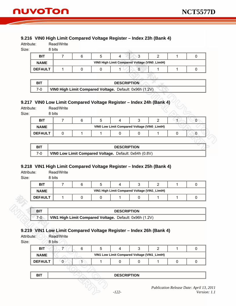
NCT5577D
Publication Release Date: April 13, 2011 -122- Version: 1.1
9.216 VIN0 High Limit Compared Voltage Register – Index 23h (Bank 4) Attribute: Read/Write Size: 8 bits
BIT 7 6 5 4 3 2 1 0 NAME VIN0 High Limit Compared Voltage (VIN0_LimtH)
DEFAULT 1 0 0 1 0 1 1 0
BIT DESCRIPTION
7-0 VIN0 High Limit Compared Voltage. Default: 0x96h (1.2V)
9.217 VIN0 Low Limit Compared Voltage Register – Index 24h (Bank 4) Attribute: Read/Write Size: 8 bits
BIT 7 6 5 4 3 2 1 0
NAME VIN0 Low Limit Compared Voltage (VIN0_LimtH)
DEFAULT 0 1 1 0 0 1 0 0
BIT DESCRIPTION
7-0 VIN0 Low Limit Compared Voltage. Default: 0x64h (0.8V)
9.218 VIN1 High Limit Compared Voltage Register – Index 25h (Bank 4) Attribute: Read/Write Size: 8 bits
BIT 7 6 5 4 3 2 1 0
NAME VIN1 High Limit Compared Voltage (VIN1_LimtH)
DEFAULT 1 0 0 1 0 1 1 0
BIT DESCRIPTION
7-0 VIN1 High Limit Compared Voltage. Default: 0x96h (1.2V)
9.219 VIN1 Low Limit Compared Voltage Register – Index 26h (Bank 4) Attribute: Read/Write Size: 8 bits
BIT 7 6 5 4 3 2 1 0 NAME VIN1 Low Limit Compared Voltage (VIN1_LimtH)
DEFAULT 0 1 1 0 0 1 0 0
BIT DESCRIPTION

NCT5577D
Publication Release Date: April 13, 2011 -123- Version: 1.1
7-0 VIN1 Low Limit Compared Voltage. Default: 0x64h (0.8V)
9.220 AVCC High Limit Compared Voltage Register – Index 27h (Bank 4) Attribute: Read/Write Size: 8 bits
BIT 7 6 5 4 3 2 1 0
NAME AVCC High Limit Compared Voltage (AVCC _LimtH)
DEFAULT 1 1 1 0 0 0 0 1
BIT DESCRIPTION
7-0 AVCC High Limit Compared Voltage. Default: 0xE1h (1.8V *2)
9.221 AVCC Low Limit Compared Voltage Register – Index 28h (Bank 4) Attribute: Read/Write Size: 8 bits
BIT 7 6 5 4 3 2 1 0 NAME AVCC Low Limit Compared Voltage (AVCC_LimtH)
DEFAULT 1 0 0 1 0 1 1 0
BIT DESCRIPTION
7-0 AVCC Low Limit Compared Voltage (AVCC_LimtH). Default: 0x96h (1.2V *2)
9.222 Reserved Register – Index 2Ah ~ 3Fh (Bank 4)
9.223 SMI_TEMP4-6 SMI# Mask Register - Index 40h (Bank 4) Attribute: Read/Write Size: 8 bits
BIT 7 6 5 4 3 2 1 0
NAME Reserved SMSK TEMP_T6_Shut
SMSK TEMP_T5_Shut
SMSK TEMP_T4_Shut
SMSK TEMP_T6
SMSK TEMP_T5
SMSK TEMP_T4
DEFAULT 0 0 1 1 1 1 1 1
BIT DESCRIPTION
7-6 Reserved. 5 SMSKTEMP_T6_Shut 4 SMSKTEMP_T5_Shut 3 SMSKTEMP_T4_Shut 2 SMSKTEMP_T6 1 SMSKTEMP_T5 0 SMSKTEMP_T4
“1” disables the corresponding interrupt status bit for the SMI interrupt. (See Interrupt Status Register 4 – Index 45h (Bank 0))
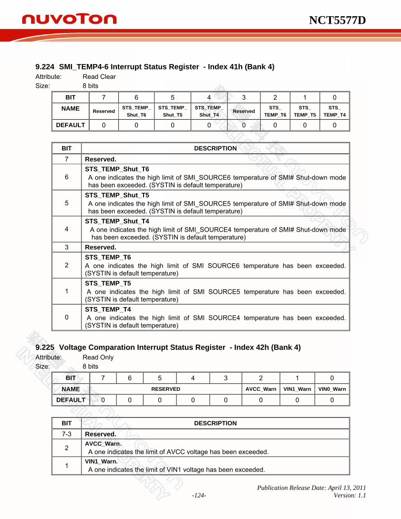
NCT5577D
Publication Release Date: April 13, 2011 -124- Version: 1.1
9.224 SMI_TEMP4-6 Interrupt Status Register - Index 41h (Bank 4) Attribute: Read Clear Size: 8 bits
BIT 7 6 5 4 3 2 1 0 NAME Reserved
STS_TEMP_ Shut_T6
STS_TEMP_Shut_T5
STS_TEMP_Shut_T4
ReservedSTS_
TEMP_T6 STS_
TEMP_T5 STS_
TEMP_T4
DEFAULT 0 0 0 0 0 0 0 0
BIT DESCRIPTION
7 Reserved.
6 STS_TEMP_Shut_T6 A one indicates the high limit of SMI_SOURCE6 temperature of SMI# Shut-down mode has been exceeded. (SYSTIN is default temperature)
5 STS_TEMP_Shut_T5 A one indicates the high limit of SMI_SOURCE5 temperature of SMI# Shut-down mode has been exceeded. (SYSTIN is default temperature)
4 STS_TEMP_Shut_T4 A one indicates the high limit of SMI_SOURCE4 temperature of SMI# Shut-down mode has been exceeded. (SYSTIN is default temperature)
3 Reserved.
2 STS_TEMP_T6 A one indicates the high limit of SMI SOURCE6 temperature has been exceeded. (SYSTIN is default temperature)
1 STS_TEMP_T5 A one indicates the high limit of SMI SOURCE5 temperature has been exceeded. (SYSTIN is default temperature)
0 STS_TEMP_T4 A one indicates the high limit of SMI SOURCE4 temperature has been exceeded. (SYSTIN is default temperature)
9.225 Voltage Comparation Interrupt Status Register - Index 42h (Bank 4) Attribute: Read Only Size: 8 bits
BIT 7 6 5 4 3 2 1 0
NAME RESERVED AVCC_Warn VIN1_Warn VIN0_Warn
DEFAULT 0 0 0 0 0 0 0 0
BIT DESCRIPTION
7-3 Reserved.
2 AVCC_Warn. A one indicates the limit of AVCC voltage has been exceeded.
1 VIN1_Warn. A one indicates the limit of VIN1 voltage has been exceeded.
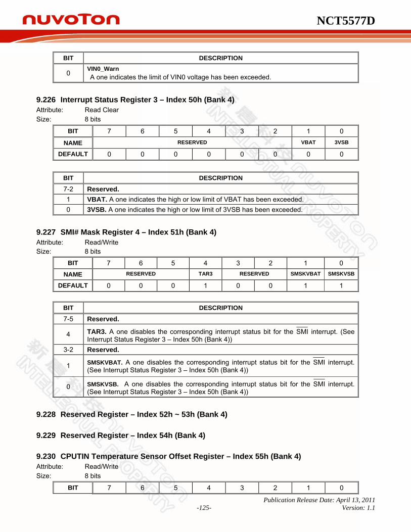
NCT5577D
Publication Release Date: April 13, 2011 -125- Version: 1.1
BIT DESCRIPTION
0 VIN0_Warn A one indicates the limit of VIN0 voltage has been exceeded.
9.226 Interrupt Status Register 3 – Index 50h (Bank 4) Attribute: Read Clear Size: 8 bits
BIT 7 6 5 4 3 2 1 0
NAME RESERVED VBAT 3VSB
DEFAULT 0 0 0 0 0 0 0 0
BIT DESCRIPTION
7-2 Reserved. 1 VBAT. A one indicates the high or low limit of VBAT has been exceeded. 0 3VSB. A one indicates the high or low limit of 3VSB has been exceeded.
9.227 SMI# Mask Register 4 – Index 51h (Bank 4) Attribute: Read/Write Size: 8 bits
BIT 7 6 5 4 3 2 1 0 NAME RESERVED TAR3 RESERVED SMSKVBAT SMSKVSB
DEFAULT 0 0 0 1 0 0 1 1
BIT DESCRIPTION
7-5 Reserved.
4 TAR3. A one disables the corresponding interrupt status bit for the SMI interrupt. (See Interrupt Status Register 3 – Index 50h (Bank 4))
3-2 Reserved.
1 SMSKVBAT. A one disables the corresponding interrupt status bit for the SMI interrupt. (See Interrupt Status Register 3 – Index 50h (Bank 4))
0 SMSKVSB. A one disables the corresponding interrupt status bit for the SMI interrupt. (See Interrupt Status Register 3 – Index 50h (Bank 4))
9.228 Reserved Register – Index 52h ~ 53h (Bank 4)
9.229 Reserved Register – Index 54h (Bank 4)
9.230 CPUTIN Temperature Sensor Offset Register – Index 55h (Bank 4) Attribute: Read/Write Size: 8 bits
BIT 7 6 5 4 3 2 1 0

NCT5577D
Publication Release Date: April 13, 2011 -126- Version: 1.1
NAME OFFSET<7:0>
DEFAULT 0 0 0 0 0 0 0 0
BIT DESCRIPTION
7-0 CPUTIN Temperature Offset Value. The value in this register will be added to the monitored value so that the read value is the sum of the monitored value and this offset value.
9.231 AUXTIN Temperature Sensor Offset Register – Index 56h (Bank 4) Attribute: Read/Write Size: 8 bits
BIT 7 6 5 4 3 2 1 0
NAME OFFSET<7:0>
DEFAULT 0 0 0 0 0 0 0 0
BIT DESCRIPTION
7-0 AUXTIN Temperature Offset Value. The value in this register is added to the monitored value so that the read value is the sum of the monitored value and this offset value.
9.232 Reserved Register – Index 57h-58h (Bank 4)
9.233 Real Time Hardware Status Register I – Index 59h (Bank 4) Attribute: Read Only Size: 8 bits
BIT 7 6 5 4 3 2 1 0
NAME CPUFANIN _STS
SYSFANIN _STS
CPUTIN_STS
Reserved. 3VCC _STS
AVCC _STS
VIN0 _STS
CPUVCORE_STS
DEFAULT 0 0 0 0 0 0 0 0
BIT DESCRIPTION
7 CPUFANIN_STS. CPUFANIN Status. 1: Fan speed count is over the threshold value. 0: Fan speed count is in the allowed range.
6 SYSFANIN_STS. SYSFANIN Status. 1: Fan speed count is over the threshold value. 0: Fan speed count is in the allowed range.
5 CPUTIN_STS. CPUTIN Temperature Sensor Status. 1: Temperature exceeds the over-temperature value. 0: Temperature is under the hysteresis value.
4 Reserved.
3 3VCC_STS. 3VCC Voltage Status. 1: 3VCC voltage is over or under the allowed range.

NCT5577D
Publication Release Date: April 13, 2011 -127- Version: 1.1
BIT DESCRIPTION 0: 3VCC voltage is in the allowed range.
2 AVCC_STS. AVCC Voltage Status. 1: AVCC voltage is over or under the allowed range. 0: AVCC voltage is in the allowed range.
1 VIN0_STS. VIN0 Voltage Status. 1: VIN0 voltage is over or under the allowed range. 0: VIN0 voltage is in the allowed range.
0 CPUVCORE_STS. CPUVCORE Voltage Status. 1: CPUVCORE voltage is over or under the allowed range. 0: CPUVCORE voltage is in the allowed range.
9.234 Real Time Hardware Status Register II – Index 5Ah (Bank 4) Attribute: Read Only Size: 8 bits
BIT 7 6 5 4 3 2 1 0 NAME TAR2
_STS TAR1 _STS
AUXTIN_STS
Reserved. Reserved. Reserved. Reserved. VIN1 _STS
DEFAULT 0 0 0 0 0 0 0 0
BIT DESCRIPTION
7
TAR2_STS. Smart Fan of CPUFANIN Warning Status. 1: Selected temperature has been over the target temperature for three minutes at full fan speed in Thermal Cruise Mode. 0: Selected temperature has not reached the warning range.
6
TAR1_STS. Smart Fan of SYSFANIN Warning Status. 1: SYSTIN temperature has been over the target temperature for three minutes at full fan speed in Thermal Cruise Mode. 0: SYSTIN temperature has not reached the warning range.
5 AUXTIN_STS. AUXTIN Temperature Sensor Status. 1: Temperature exceeds the over-temperature value. 0: Temperature is under the hysteresis value.
4~1 Reserved.
0 VIN1_STS. VIN1 Voltage Status. 1: VIN1 voltage is over or under the allowed range. 0: VIN1 voltage is in the allowed range.
9.235 Real Time Hardware Status Register III – Index 5Bh (Bank 4) Attribute: Read Only Size: 8 bits
BIT 7 6 5 4 3 2 1 0 NAME RESERVED VIN3
_STS RESERVED VBAT
_STS VSB _STS
DEFAULT 0 0 0 0 0 0 0 0

NCT5577D
Publication Release Date: April 13, 2011 -128- Version: 1.1
BIT DESCRIPTION
7~5 Reserved.
4 VIN3_STS. VIN3 Voltage Status. 1: VIN3 voltage is over or under the allowed range. 0: VIN3 voltage is in the allowed range.
3~2 Reserved.
1 VBAT_STS. VBAT Voltage Status. 1: The VBAT voltage is over or under the allowed range. 0: The VBAT voltage is in the allowed range.
0 VSB_STS. 3VSB Voltage Status. 1: The 3VSB voltage is over or under the allowed range. 0: The 3VSB voltage is in the allowed range.
9.236 Reserved Register – Index 5Ch ~ 5Fh (Bank 4)
9.237 Is<8:1> Current Register – Index 60h (Bank 4) Attribute: Read Only Size: 8 bits
BIT 7 6 5 4 3 2 1 0 NAME Is<8:1>
DEFAULT 0 0 0 0 0 0 0 0
BIT DESCRIPTION
7-0 Is<8:1>. Current measure by current measure IC (1LSB=31.25mA)
9.238 Is<0> Current Register – Index 61h (Bank 4) Attribute: Read Only Size: 8 bits
BIT 7 6 5 4 3 2 1 0
NAME Reserved Is<0>
DEFAULT 0 0 0 0 0 0 0 0
BIT DESCRIPTION
7-1 Reserved
0 Is<0>. Current measure by current measure IC (1LSB=31.25mA)
9.239 POWER <9:2> Register – Index 62h (Bank 4) Attribute: Read Only Size: 8 bits
BIT 7 6 5 4 3 2 1 0
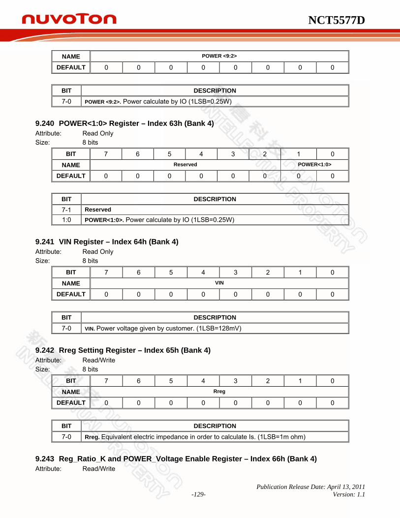
NCT5577D
Publication Release Date: April 13, 2011 -129- Version: 1.1
NAME POWER <9:2>
DEFAULT 0 0 0 0 0 0 0 0
BIT DESCRIPTION
7-0 POWER <9:2>. Power calculate by IO (1LSB=0.25W)
9.240 POWER<1:0> Register – Index 63h (Bank 4) Attribute: Read Only Size: 8 bits
BIT 7 6 5 4 3 2 1 0
NAME Reserved POWER<1:0>
DEFAULT 0 0 0 0 0 0 0 0
BIT DESCRIPTION
7-1 Reserved
1:0 POWER<1:0>. Power calculate by IO (1LSB=0.25W)
9.241 VIN Register – Index 64h (Bank 4) Attribute: Read Only Size: 8 bits
BIT 7 6 5 4 3 2 1 0 NAME VIN
DEFAULT 0 0 0 0 0 0 0 0
BIT DESCRIPTION
7-0 VIN. Power voltage given by customer. (1LSB=128mV)
9.242 Rreg Setting Register – Index 65h (Bank 4) Attribute: Read/Write Size: 8 bits
BIT 7 6 5 4 3 2 1 0
NAME Rreg
DEFAULT 0 0 0 0 0 0 0 0
BIT DESCRIPTION
7-0 Rreg. Equivalent electric impedance in order to calculate Is. (1LSB=1m ohm)
9.243 Reg_Ratio_K and POWER_Voltage Enable Register – Index 66h (Bank 4) Attribute: Read/Write
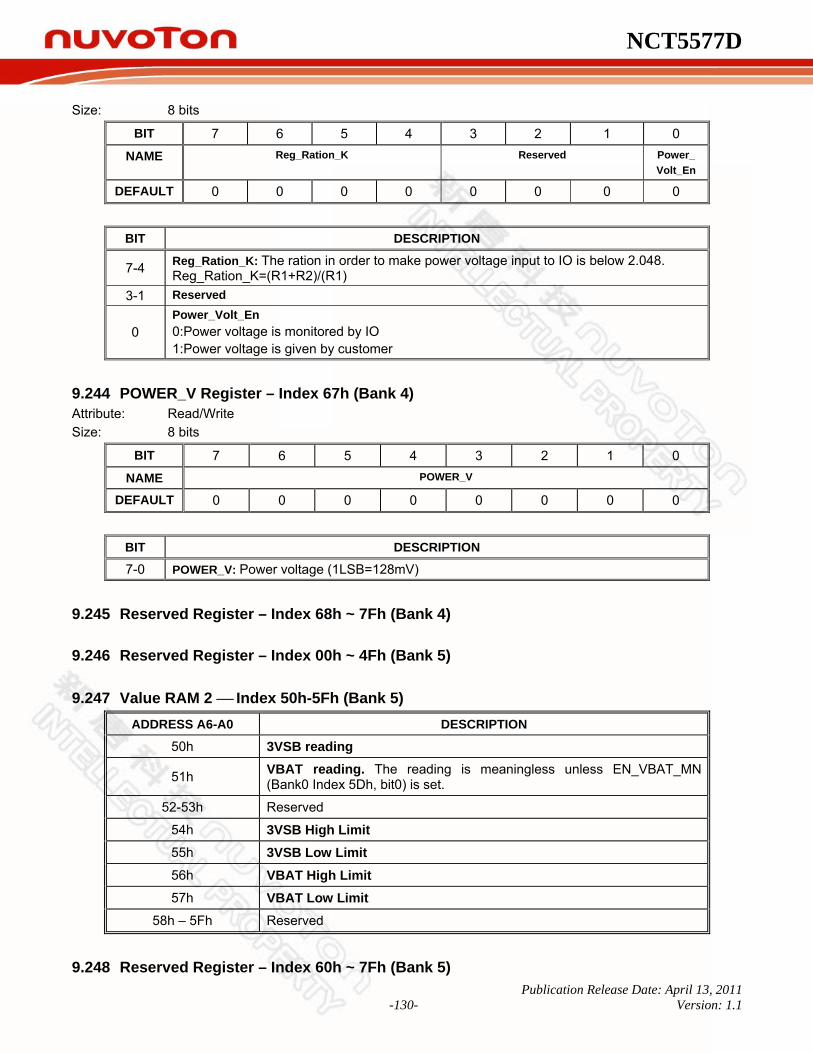
NCT5577D
Publication Release Date: April 13, 2011 -130- Version: 1.1
Size: 8 bits
BIT 7 6 5 4 3 2 1 0
NAME Reg_Ration_K Reserved Power_ Volt_En
DEFAULT 0 0 0 0 0 0 0 0
BIT DESCRIPTION
7-4 Reg_Ration_K: The ration in order to make power voltage input to IO is below 2.048. Reg_Ration_K=(R1+R2)/(R1)
3-1 Reserved
0 Power_Volt_En 0:Power voltage is monitored by IO 1:Power voltage is given by customer
9.244 POWER_V Register – Index 67h (Bank 4) Attribute: Read/Write Size: 8 bits
BIT 7 6 5 4 3 2 1 0
NAME POWER_V
DEFAULT 0 0 0 0 0 0 0 0
BIT DESCRIPTION
7-0 POWER_V: Power voltage (1LSB=128mV)
9.245 Reserved Register – Index 68h ~ 7Fh (Bank 4)
9.246 Reserved Register – Index 00h ~ 4Fh (Bank 5)
9.247 Value RAM 2 ⎯ Index 50h-5Fh (Bank 5) ADDRESS A6-A0 DESCRIPTION
50h 3VSB reading
51h VBAT reading. The reading is meaningless unless EN_VBAT_MN (Bank0 Index 5Dh, bit0) is set.
52-53h Reserved
54h 3VSB High Limit 55h 3VSB Low Limit 56h VBAT High Limit 57h VBAT Low Limit
58h – 5Fh Reserved
9.248 Reserved Register – Index 60h ~ 7Fh (Bank 5)
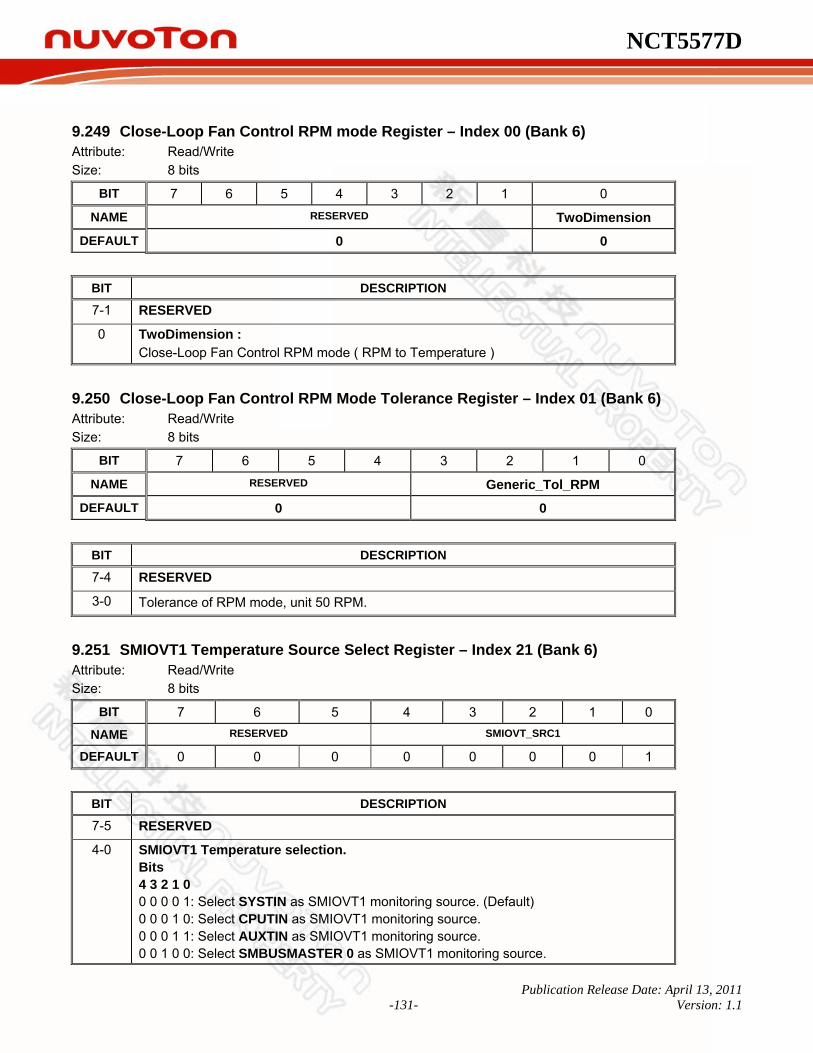
NCT5577D
Publication Release Date: April 13, 2011 -131- Version: 1.1
9.249 Close-Loop Fan Control RPM mode Register – Index 00 (Bank 6) Attribute: Read/Write Size: 8 bits
BIT 7 6 5 4 3 2 1 0
NAME RESERVED TwoDimension
DEFAULT 0 0
BIT DESCRIPTION
7-1 RESERVED
0 TwoDimension : Close-Loop Fan Control RPM mode ( RPM to Temperature )
9.250 Close-Loop Fan Control RPM Mode Tolerance Register – Index 01 (Bank 6) Attribute: Read/Write Size: 8 bits
BIT 7 6 5 4 3 2 1 0
NAME RESERVED Generic_Tol_RPM
DEFAULT 0 0
BIT DESCRIPTION
7-4 RESERVED
3-0 Tolerance of RPM mode, unit 50 RPM.
9.251 SMIOVT1 Temperature Source Select Register – Index 21 (Bank 6) Attribute: Read/Write Size: 8 bits
BIT 7 6 5 4 3 2 1 0
NAME RESERVED SMIOVT_SRC1
DEFAULT 0 0 0 0 0 0 0 1
BIT DESCRIPTION
7-5 RESERVED
4-0 SMIOVT1 Temperature selection. Bits 4 3 2 1 0 0 0 0 0 1: Select SYSTIN as SMIOVT1 monitoring source. (Default) 0 0 0 1 0: Select CPUTIN as SMIOVT1 monitoring source. 0 0 0 1 1: Select AUXTIN as SMIOVT1 monitoring source. 0 0 1 0 0: Select SMBUSMASTER 0 as SMIOVT1 monitoring source.
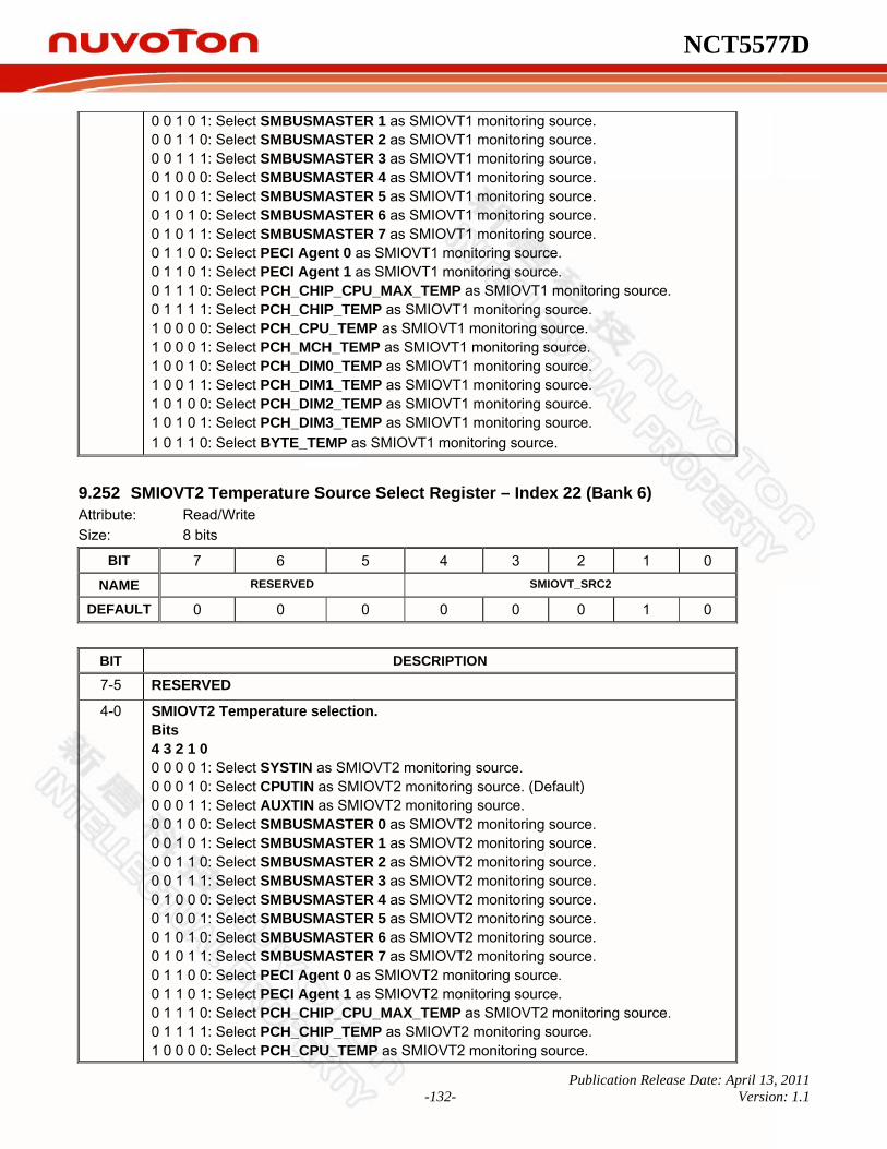
NCT5577D
Publication Release Date: April 13, 2011 -132- Version: 1.1
0 0 1 0 1: Select SMBUSMASTER 1 as SMIOVT1 monitoring source. 0 0 1 1 0: Select SMBUSMASTER 2 as SMIOVT1 monitoring source. 0 0 1 1 1: Select SMBUSMASTER 3 as SMIOVT1 monitoring source. 0 1 0 0 0: Select SMBUSMASTER 4 as SMIOVT1 monitoring source. 0 1 0 0 1: Select SMBUSMASTER 5 as SMIOVT1 monitoring source. 0 1 0 1 0: Select SMBUSMASTER 6 as SMIOVT1 monitoring source. 0 1 0 1 1: Select SMBUSMASTER 7 as SMIOVT1 monitoring source. 0 1 1 0 0: Select PECI Agent 0 as SMIOVT1 monitoring source. 0 1 1 0 1: Select PECI Agent 1 as SMIOVT1 monitoring source. 0 1 1 1 0: Select PCH_CHIP_CPU_MAX_TEMP as SMIOVT1 monitoring source. 0 1 1 1 1: Select PCH_CHIP_TEMP as SMIOVT1 monitoring source. 1 0 0 0 0: Select PCH_CPU_TEMP as SMIOVT1 monitoring source. 1 0 0 0 1: Select PCH_MCH_TEMP as SMIOVT1 monitoring source. 1 0 0 1 0: Select PCH_DIM0_TEMP as SMIOVT1 monitoring source. 1 0 0 1 1: Select PCH_DIM1_TEMP as SMIOVT1 monitoring source. 1 0 1 0 0: Select PCH_DIM2_TEMP as SMIOVT1 monitoring source. 1 0 1 0 1: Select PCH_DIM3_TEMP as SMIOVT1 monitoring source. 1 0 1 1 0: Select BYTE_TEMP as SMIOVT1 monitoring source.
9.252 SMIOVT2 Temperature Source Select Register – Index 22 (Bank 6) Attribute: Read/Write Size: 8 bits
BIT 7 6 5 4 3 2 1 0 NAME RESERVED SMIOVT_SRC2
DEFAULT 0 0 0 0 0 0 1 0
BIT DESCRIPTION
7-5 RESERVED
4-0 SMIOVT2 Temperature selection. Bits 4 3 2 1 0 0 0 0 0 1: Select SYSTIN as SMIOVT2 monitoring source. 0 0 0 1 0: Select CPUTIN as SMIOVT2 monitoring source. (Default) 0 0 0 1 1: Select AUXTIN as SMIOVT2 monitoring source. 0 0 1 0 0: Select SMBUSMASTER 0 as SMIOVT2 monitoring source. 0 0 1 0 1: Select SMBUSMASTER 1 as SMIOVT2 monitoring source. 0 0 1 1 0: Select SMBUSMASTER 2 as SMIOVT2 monitoring source. 0 0 1 1 1: Select SMBUSMASTER 3 as SMIOVT2 monitoring source. 0 1 0 0 0: Select SMBUSMASTER 4 as SMIOVT2 monitoring source. 0 1 0 0 1: Select SMBUSMASTER 5 as SMIOVT2 monitoring source. 0 1 0 1 0: Select SMBUSMASTER 6 as SMIOVT2 monitoring source. 0 1 0 1 1: Select SMBUSMASTER 7 as SMIOVT2 monitoring source. 0 1 1 0 0: Select PECI Agent 0 as SMIOVT2 monitoring source. 0 1 1 0 1: Select PECI Agent 1 as SMIOVT2 monitoring source. 0 1 1 1 0: Select PCH_CHIP_CPU_MAX_TEMP as SMIOVT2 monitoring source. 0 1 1 1 1: Select PCH_CHIP_TEMP as SMIOVT2 monitoring source. 1 0 0 0 0: Select PCH_CPU_TEMP as SMIOVT2 monitoring source.
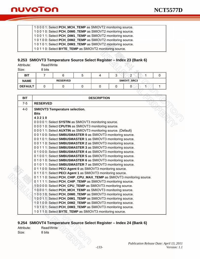
NCT5577D
Publication Release Date: April 13, 2011 -133- Version: 1.1
1 0 0 0 1: Select PCH_MCH_TEMP as SMIOVT2 monitoring source. 1 0 0 1 0: Select PCH_DIM0_TEMP as SMIOVT2 monitoring source. 1 0 0 1 1: Select PCH_DIM1_TEMP as SMIOVT2 monitoring source. 1 0 1 0 0: Select PCH_DIM2_TEMP as SMIOVT2 monitoring source. 1 0 1 0 1: Select PCH_DIM3_TEMP as SMIOVT2 monitoring source. 1 0 1 1 0: Select BYTE_TEMP as SMIOVT2 monitoring source.
9.253 SMIOVT3 Temperature Source Select Register – Index 23 (Bank 6) Attribute: Read/Write Size: 8 bits
BIT 7 6 5 4 3 2 1 0 NAME RESERVED SMIOVT_SRC3
DEFAULT 0 0 0 0 0 0 1 1
BIT DESCRIPTION
7-5 RESERVED
4-0 SMIOVT3 Temperature selection. Bits 4 3 2 1 0 0 0 0 0 1: Select SYSTIN as SMIOVT3 monitoring source. 0 0 0 1 0: Select CPUTIN as SMIOVT3 monitoring source. 0 0 0 1 1: Select AUXTIN as SMIOVT3 monitoring source. (Default) 0 0 1 0 0: Select SMBUSMASTER 0 as SMIOVT3 monitoring source. 0 0 1 0 1: Select SMBUSMASTER 1 as SMIOVT3 monitoring source. 0 0 1 1 0: Select SMBUSMASTER 2 as SMIOVT3 monitoring source. 0 0 1 1 1: Select SMBUSMASTER 3 as SMIOVT3 monitoring source. 0 1 0 0 0: Select SMBUSMASTER 4 as SMIOVT3 monitoring source. 0 1 0 0 1: Select SMBUSMASTER 5 as SMIOVT3 monitoring source. 0 1 0 1 0: Select SMBUSMASTER 6 as SMIOVT3 monitoring source. 0 1 0 1 1: Select SMBUSMASTER 7 as SMIOVT3 monitoring source. 0 1 1 0 0: Select PECI Agent 0 as SMIOVT3 monitoring source. 0 1 1 0 1: Select PECI Agent 1 as SMIOVT3 monitoring source. 0 1 1 1 0: Select PCH_CHIP_CPU_MAX_TEMP as SMIOVT3 monitoring source. 0 1 1 1 1: Select PCH_CHIP_TEMP as SMIOVT3 monitoring source. 1 0 0 0 0: Select PCH_CPU_TEMP as SMIOVT3 monitoring source. 1 0 0 0 1: Select PCH_MCH_TEMP as SMIOVT3 monitoring source. 1 0 0 1 0: Select PCH_DIM0_TEMP as SMIOVT3 monitoring source. 1 0 0 1 1: Select PCH_DIM1_TEMP as SMIOVT3 monitoring source. 1 0 1 0 0: Select PCH_DIM2_TEMP as SMIOVT3 monitoring source. 1 0 1 0 1: Select PCH_DIM3_TEMP as SMIOVT3 monitoring source. 1 0 1 1 0: Select BYTE_TEMP as SMIOVT3 monitoring source.
9.254 SMIOVT4 Temperature Source Select Register – Index 24 (Bank 6) Attribute: Read/Write Size: 8 bits

NCT5577D
Publication Release Date: April 13, 2011 -134- Version: 1.1
BIT 7 6 5 4 3 2 1 0 NAME RESERVED SMIOVT_SRC4
DEFAULT 0 0 0 0 0 0 0 1
BIT DESCRIPTION
7-5 RESERVED
4-0 SMIOVT4 Temperature selection. Bits 4 3 2 1 0 0 0 0 0 1: Select SYSTIN as SMIOVT4 monitoring source. (Default) 0 0 0 1 0: Select CPUTIN as SMIOVT4 monitoring source. 0 0 0 1 1: Select AUXTIN as SMIOVT4 monitoring source. 0 0 1 0 0: Select SMBUSMASTER 0 as SMIOVT4 monitoring source. 0 0 1 0 1: Select SMBUSMASTER 1 as SMIOVT4 monitoring source. 0 0 1 1 0: Select SMBUSMASTER 2 as SMIOVT4 monitoring source. 0 0 1 1 1: Select SMBUSMASTER 3 as SMIOVT4 monitoring source. 0 1 0 0 0: Select SMBUSMASTER 4 as SMIOVT4 monitoring source. 0 1 0 0 1: Select SMBUSMASTER 5 as SMIOVT4 monitoring source. 0 1 0 1 0: Select SMBUSMASTER 6 as SMIOVT4 monitoring source. 0 1 0 1 1: Select SMBUSMASTER 7 as SMIOVT4 monitoring source. 0 1 1 0 0: Select PECI Agent 0 as SMIOVT4 monitoring source. 0 1 1 0 1: Select PECI Agent 1 as SMIOVT4 monitoring source. 0 1 1 1 0: Select PCH_CHIP_CPU_MAX_TEMP as SMIOVT4 monitoring source. 0 1 1 1 1: Select PCH_CHIP_TEMP as SMIOVT4 monitoring source. 1 0 0 0 0: Select PCH_CPU_TEMP as SMIOVT4 monitoring source. 1 0 0 0 1: Select PCH_MCH_TEMP as SMIOVT4 monitoring source. 1 0 0 1 0: Select PCH_DIM0_TEMP as SMIOVT4 monitoring source. 1 0 0 1 1: Select PCH_DIM1_TEMP as SMIOVT4 monitoring source. 1 0 1 0 0: Select PCH_DIM2_TEMP as SMIOVT4 monitoring source. 1 0 1 0 1: Select PCH_DIM3_TEMP as SMIOVT4 monitoring source. 1 0 1 1 0: Select BYTE_TEMP as SMIOVT4 monitoring source.
9.255 SMIOVT5 Temperature Source Select Register – Index 25 (Bank 6) Attribute: Read/Write Size: 8 bits
BIT 7 6 5 4 3 2 1 0 NAME RESERVED SMIOVT_SRC5
DEFAULT 0 0 0 0 0 0 0 1
BIT DESCRIPTION
7-5 RESERVED
4-0 SMIOVT5 Temperature selection. Bits 4 3 2 1 0 0 0 0 0 1: Select SYSTIN as SMIOVT5 monitoring source. (Default)

NCT5577D
Publication Release Date: April 13, 2011 -135- Version: 1.1
0 0 0 1 0: Select CPUTIN as SMIOVT5 monitoring source. 0 0 0 1 1: Select AUXTIN as SMIOVT5 monitoring source. 0 0 1 0 0: Select SMBUSMASTER 0 as SMIOVT5 monitoring source. 0 0 1 0 1: Select SMBUSMASTER 1 as SMIOVT5 monitoring source. 0 0 1 1 0: Select SMBUSMASTER 2 as SMIOVT5 monitoring source. 0 0 1 1 1: Select SMBUSMASTER 3 as SMIOVT5 monitoring source. 0 1 0 0 0: Select SMBUSMASTER 4 as SMIOVT5 monitoring source. 0 1 0 0 1: Select SMBUSMASTER 5 as SMIOVT5 monitoring source. 0 1 0 1 0: Select SMBUSMASTER 6 as SMIOVT5 monitoring source. 0 1 0 1 1: Select SMBUSMASTER 7 as SMIOVT5 monitoring source. 0 1 1 0 0: Select PECI Agent 0 as SMIOVT5 monitoring source. 0 1 1 0 1: Select PECI Agent 1 as SMIOVT5 monitoring source. 0 1 1 1 0: Select PCH_CHIP_CPU_MAX_TEMP as SMIOVT5 monitoring source. 0 1 1 1 1: Select PCH_CHIP_TEMP as SMIOVT5 monitoring source. 1 0 0 0 0: Select PCH_CPU_TEMP as SMIOVT5 monitoring source. 1 0 0 0 1: Select PCH_MCH_TEMP as SMIOVT5 monitoring source. 1 0 0 1 0: Select PCH_DIM0_TEMP as SMIOVT5 monitoring source. 1 0 0 1 1: Select PCH_DIM1_TEMP as SMIOVT5 monitoring source. 1 0 1 0 0: Select PCH_DIM2_TEMP as SMIOVT5 monitoring source. 1 0 1 0 1: Select PCH_DIM3_TEMP as SMIOVT5 monitoring source. 1 0 1 1 0: Select BYTE_TEMP as SMIOVT5 monitoring source.
9.256 SMIOVT6 Temperature Source Select Register – Index 26 (Bank 6) Attribute: Read/Write Size: 8 bits
BIT 7 6 5 4 3 2 1 0 NAME RESERVED SMIOVT_SRC6
DEFAULT 0 0 0 0 0 0 0 1
BIT DESCRIPTION
7-5 RESERVED
4-0 SMIOVT6 Temperature selection. Bits 4 3 2 1 0 0 0 0 0 1: Select SYSTIN as SMIOVT6 monitoring source. (Default) 0 0 0 1 0: Select CPUTIN as SMIOVT6 monitoring source. 0 0 0 1 1: Select AUXTIN as SMIOVT6 monitoring source. 0 0 1 0 0: Select SMBUSMASTER 0 as SMIOVT6 monitoring source. 0 0 1 0 1: Select SMBUSMASTER 1 as SMIOVT6 monitoring source. 0 0 1 1 0: Select SMBUSMASTER 2 as SMIOVT6 monitoring source. 0 0 1 1 1: Select SMBUSMASTER 3 as SMIOVT6 monitoring source. 0 1 0 0 0: Select SMBUSMASTER 4 as SMIOVT6 monitoring source. 0 1 0 0 1: Select SMBUSMASTER 5 as SMIOVT6 monitoring source. 0 1 0 1 0: Select SMBUSMASTER 6 as SMIOVT6 monitoring source. 0 1 0 1 1: Select SMBUSMASTER 7 as SMIOVT6 monitoring source. 0 1 1 0 0: Select PECI Agent 0 as SMIOVT6 monitoring source. 0 1 1 0 1: Select PECI Agent 1 as SMIOVT6 monitoring source.

NCT5577D
Publication Release Date: April 13, 2011 -136- Version: 1.1
0 1 1 1 0: Select PCH_CHIP_CPU_MAX_TEMP as SMIOVT6 monitoring source. 0 1 1 1 1: Select PCH_CHIP_TEMP as SMIOVT6 monitoring source. 1 0 0 0 0: Select PCH_CPU_TEMP as SMIOVT6 monitoring source. 1 0 0 0 1: Select PCH_MCH_TEMP as SMIOVT6 monitoring source. 1 0 0 1 0: Select PCH_DIM0_TEMP as SMIOVT6 monitoring source. 1 0 0 1 1: Select PCH_DIM1_TEMP as SMIOVT6 monitoring source. 1 0 1 0 0: Select PCH_DIM2_TEMP as SMIOVT6 monitoring source. 1 0 1 0 1: Select PCH_DIM3_TEMP as SMIOVT6 monitoring source. 1 0 1 1 0: Select BYTE_TEMP as SMIOVT6 monitoring source.
9.257 Reserved Register – Index 27h (Bank 6)
9.258 SMIOVT4 Temperature Source Configuration Register – Index 28h (Bank 6) Attribute: Read/Write Size: 8 bits
BIT 7 6 5 4 3 2 1 0 NAME RESERVED FAULT RESERVED OVTMOD STOP
DEFAULT 0 0 0 0 0 0 0 0
BIT DESCRIPTION
7-5 Reserved. This bit should be set to zero.
4-3 Fault. Number of faults to detect before setting OVT# output. This avoids false strapping due to noise.
2 Reserved. This bit should be set to zero.
1 OVTMOD. SMIOVT4 Mode Select. 0: Compare Mode. (Default) 1: Interrupt Mode.
0 STOP. 0: Monitor SMIOVT4 temperature source. 1: Stop monitoring SMIOVT4 temperature source.
9.259 SMIOVT5 Temperature Source Configuration Register – Index 29h (Bank 6) Attribute: Read/Write Size: 8 bits
BIT 7 6 5 4 3 2 1 0
NAME RESERVED FAULT RESERVED OVTMOD STOP
DEFAULT 0 0 0 0 0 0 0 0
BIT DESCRIPTION
7-5 Reserved. This bit should be set to zero.
4-3 Fault. Number of faults to detect before setting OVT# output. This avoids false strapping due to noise.
2 Reserved. This bit should be set to zero. 1 OVTMOD. SMIOVT5 Mode Select.

NCT5577D
Publication Release Date: April 13, 2011 -137- Version: 1.1
BIT DESCRIPTION 0: Compare Mode. (Default) 1: Interrupt Mode.
0 STOP. 0: Monitor SMIOVT5 temperature source. 1: Stop monitoring SMIOVT5 temperature source.
9.260 SMIOVT6 Temperature Source Configuration Register – Index 2Ah (Bank 6) Attribute: Read/Write Size: 8 bits
BIT 7 6 5 4 3 2 1 0
NAME RESERVED FAULT RESERVED OVTMOD STOP
DEFAULT 0 0 0 0 0 0 0 0
BIT DESCRIPTION
7-5 Reserved. This bit should be set to zero.
4-3 Fault. Number of faults to detect before setting OVT# output. This avoids false strapping due to noise.
2 Reserved. This bit should be set to zero.
1 OVTMOD. SMIOVT6 Mode Select. 0: Compare Mode. (Default) 1: Interrupt Mode.
0 STOP. 0: Monitor SMIOVT6 temperature source. 1: Stop monitoring SMIOVT6 temperature source.
9.261 SMIOVT4 Temperature Source (High Byte) Register – Index 2Bh (Bank 6) Attribute: Read Only Size: 8 bits
BIT 7 6 5 4 3 2 1 0 NAME TEMP<8:1>
BIT DESCRIPTION
7-0 TEMP<8:1> (default: SYSTIN temperature source). The nine-bit value is in units of 0.5°C.
9.262 SMIOVT5 Temperature Source (High Byte) Register – Index 2Ch (Bank 6) Attribute: Read Only Size: 8 bits
BIT 7 6 5 4 3 2 1 0
NAME TEMP<8:1>
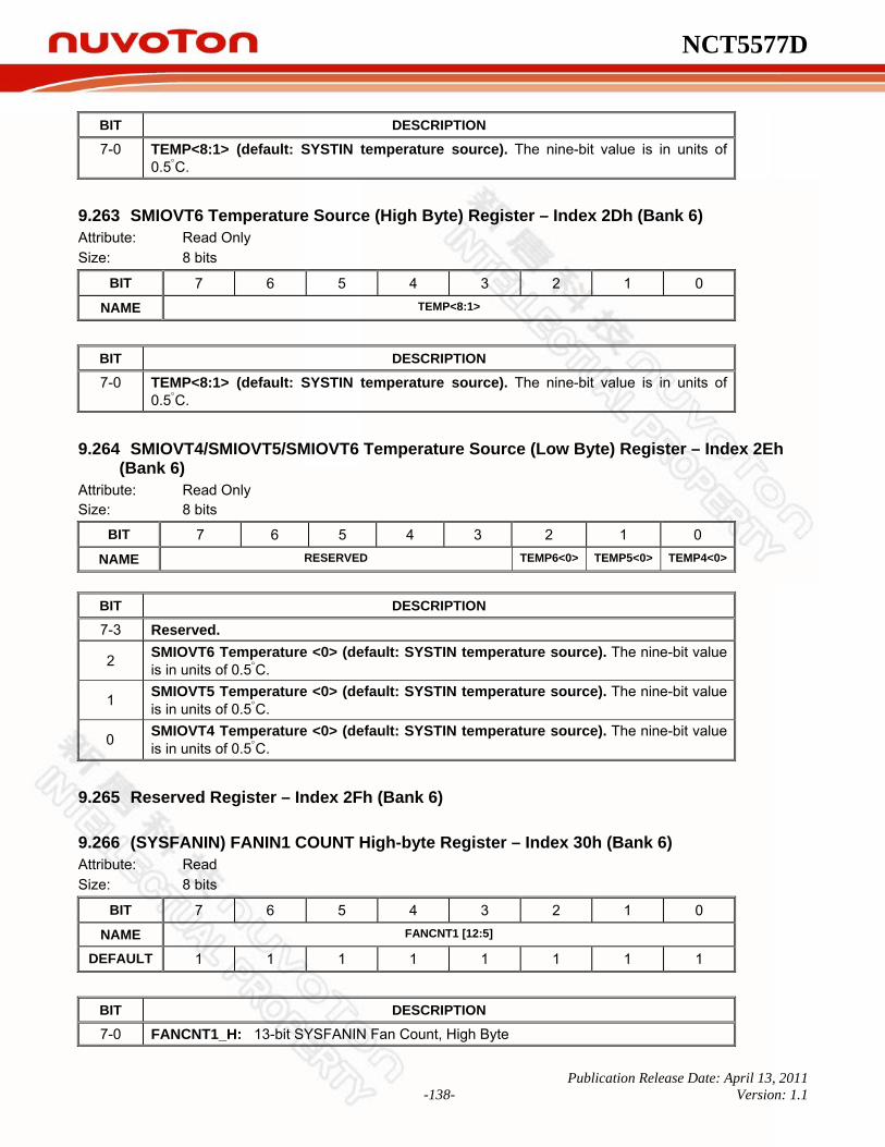
NCT5577D
Publication Release Date: April 13, 2011 -138- Version: 1.1
BIT DESCRIPTION
7-0 TEMP<8:1> (default: SYSTIN temperature source). The nine-bit value is in units of 0.5°C.
9.263 SMIOVT6 Temperature Source (High Byte) Register – Index 2Dh (Bank 6) Attribute: Read Only Size: 8 bits
BIT 7 6 5 4 3 2 1 0
NAME TEMP<8:1>
BIT DESCRIPTION
7-0 TEMP<8:1> (default: SYSTIN temperature source). The nine-bit value is in units of 0.5°C.
9.264 SMIOVT4/SMIOVT5/SMIOVT6 Temperature Source (Low Byte) Register – Index 2Eh (Bank 6)
Attribute: Read Only Size: 8 bits
BIT 7 6 5 4 3 2 1 0
NAME RESERVED TEMP6<0> TEMP5<0> TEMP4<0>
BIT DESCRIPTION
7-3 Reserved.
2 SMIOVT6 Temperature <0> (default: SYSTIN temperature source). The nine-bit value is in units of 0.5°C.
1 SMIOVT5 Temperature <0> (default: SYSTIN temperature source). The nine-bit value is in units of 0.5°C.
0 SMIOVT4 Temperature <0> (default: SYSTIN temperature source). The nine-bit value is in units of 0.5°C.
9.265 Reserved Register – Index 2Fh (Bank 6)
9.266 (SYSFANIN) FANIN1 COUNT High-byte Register – Index 30h (Bank 6) Attribute: Read Size: 8 bits
BIT 7 6 5 4 3 2 1 0 NAME FANCNT1 [12:5]
DEFAULT 1 1 1 1 1 1 1 1
BIT DESCRIPTION
7-0 FANCNT1_H: 13-bit SYSFANIN Fan Count, High Byte

NCT5577D
Publication Release Date: April 13, 2011 -139- Version: 1.1
9.267 (SYSFANIN) FANIN1 COUNT Low-byte Register – Index 31h (Bank 6) Attribute: Read Size: 8 bits
BIT 7 6 5 4 3 2 1 0
NAME RESERVED FANCNT1 [4:0]
DEFAULT 0 1F
BIT DESCRIPTION
7-5 Reserved. 4-0 FANCNT1_L: 13-bit SYSFANIN Fan Count, Low Byte
9.268 (CPUFANIN) FANIN2 COUNT High-byte Register – Index 32h (Bank 6) Attribute: Read Size: 8 bits
BIT 7 6 5 4 3 2 1 0 NAME FANCNT2 [12:5]
DEFAULT 1 1 1 1 1 1 1 1
BIT DESCRIPTION
7-0 FANCNT2_H: 13-bit SYSFANIN Fan Count, High Byte
9.269 (CPUFANIN) FANIN2 COUNT Low-byte Register – Index 33h (Bank 6) Attribute: Read Size: 8 bits
BIT 7 6 5 4 3 2 1 0
NAME RESERVED FANCNT2[4:0]
DEFAULT 0 1F
BIT DESCRIPTION
7-5 Reserved. 4-0 FANCNT2_L: 13-bit SYSFANIN Fan Count, Low Byte
9.270 Reserved Register – Index 34h (Bank 6)
9.271 Reserved Register – Index 35h (Bank 6)
9.272 Reserved Register – Index 36h (Bank 6)
9.273 Reserved Register – Index 37h (Bank 6)

NCT5577D
Publication Release Date: April 13, 2011 -140- Version: 1.1
9.274 Reserved Register – Index 38h (Bank 6)
9.275 Reserved Register – Index 39h (Bank 6)
9.276 (SYSFANIN) Fan Count Limit High-byte Register – Index 3Ah (Bank 6) Attribute: Read / Write Size: 8 bits
BIT 7 6 5 4 3 2 1 0
NAME FANIN1_HL [12:5]
DEFAULT 0 0 0 0 0 0 0 0
BIT DESCRIPTION
7-0 FANIN1_HL: 13-bit SYSFANIN Fan Count Limit, High Byte
9.277 (SYSFANIN) Fan Count Limit Low-byte Register – Index 3Bh (Bank 6) Attribute: Read / Write Size: 8 bits
BIT 7 6 5 4 3 2 1 0
NAME RESERVED FANIN1_HL [4:0]
DEFAULT 0 0
BIT DESCRIPTION
7-5 Reserved. 4-0 FANIN1_HL: 13-bit SYSFANIN Fan Count Limit, Low Byte
9.278 (CPUFANIN) Fan Count Limit High-byte Register – Index 3Ch (Bank 6) Attribute: Read / Write Size: 8 bits
BIT 7 6 5 4 3 2 1 0
NAME FANIN2_HL [12:5]
DEFAULT 0 0 0 0 0 0 0 0
BIT DESCRIPTION
7-0 FANIN2_HL: 13-bit SYSFANIN Fan Count Limit, High Byte
9.279 (CPUFANIN) Fan Count Limit Low-byte Register – Index 3Dh (Bank 6) Attribute: Read / Write Size: 8 bits
BIT 7 6 5 4 3 2 1 0

NCT5577D
Publication Release Date: April 13, 2011 -141- Version: 1.1
NAME RESERVED FANIN2_HL [4:0]
DEFAULT 0 0
BIT DESCRIPTION
7-5 Reserved. 4-0 FANIN2_HL: 13-bit SYSFANIN Fan Count Limit, Low Byte
9.280 Reserved Register – Index 3Eh (Bank 6)
9.281 Reserved Register – Index 3Fh (Bank 6)
9.282 Reserved Register – Index 40h (Bank 6)
9.283 Reserved Register – Index 41h (Bank 6)
9.284 Reserved Register – Index 42h (Bank 6)
9.285 Reserved Register – Index 43h (Bank 6)
9.286 SYSFANIN Revolution Pulses Selection Register – Index 44h (Bank 6) Attribute: Read /Write Size: 8 bits
BIT 7 6 5 4 3 2 1 0
NAME Reserved HM_Rev_Pulse_Fan1_Sel
DEFAULT 0 0 0 0 0 0 1 0
BIT DESCRIPTION
7-2 Reserved 1-0 SYSFANIN Revolution Pulses Selection
= 00, four pulses per revolution. = 01, one pulse per revolution. = 10, two pulses per revolution. (default) = 11, three pulses per revolution.
9.287 CPUFANIN Revolution Pulses Selection Register – Index 45h (Bank 6) Attribute: Read /Write Size: 8 bits
BIT 7 6 5 4 3 2 1 0
NAME Reserved HM_Rev_Pulse_Fan2_Sel
DEFAULT 0 0 0 0 0 0 1 0
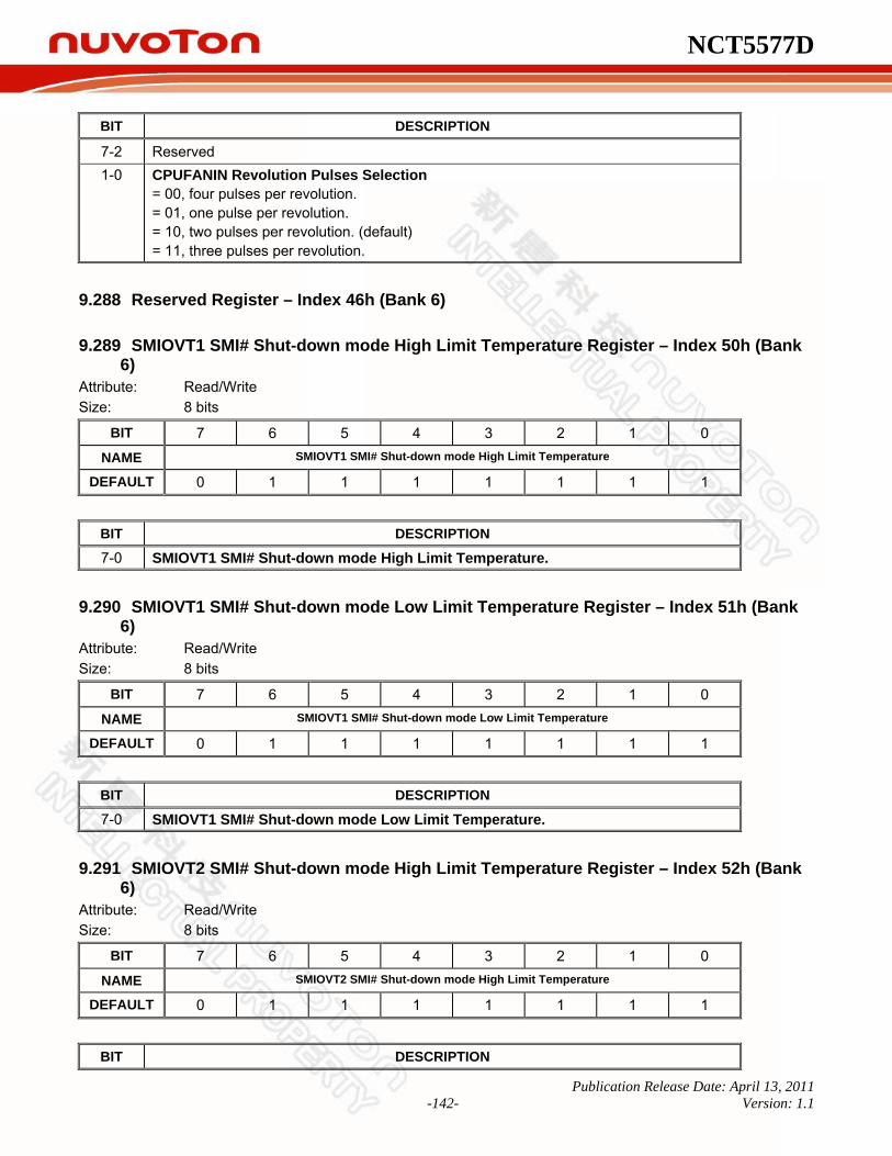
NCT5577D
Publication Release Date: April 13, 2011 -142- Version: 1.1
BIT DESCRIPTION
7-2 Reserved 1-0 CPUFANIN Revolution Pulses Selection
= 00, four pulses per revolution. = 01, one pulse per revolution. = 10, two pulses per revolution. (default) = 11, three pulses per revolution.
9.288 Reserved Register – Index 46h (Bank 6)
9.289 SMIOVT1 SMI# Shut-down mode High Limit Temperature Register – Index 50h (Bank 6)
Attribute: Read/Write Size: 8 bits
BIT 7 6 5 4 3 2 1 0 NAME SMIOVT1 SMI# Shut-down mode High Limit Temperature
DEFAULT 0 1 1 1 1 1 1 1
BIT DESCRIPTION
7-0 SMIOVT1 SMI# Shut-down mode High Limit Temperature.
9.290 SMIOVT1 SMI# Shut-down mode Low Limit Temperature Register – Index 51h (Bank 6)
Attribute: Read/Write Size: 8 bits
BIT 7 6 5 4 3 2 1 0
NAME SMIOVT1 SMI# Shut-down mode Low Limit Temperature
DEFAULT 0 1 1 1 1 1 1 1
BIT DESCRIPTION
7-0 SMIOVT1 SMI# Shut-down mode Low Limit Temperature.
9.291 SMIOVT2 SMI# Shut-down mode High Limit Temperature Register – Index 52h (Bank 6)
Attribute: Read/Write Size: 8 bits
BIT 7 6 5 4 3 2 1 0
NAME SMIOVT2 SMI# Shut-down mode High Limit Temperature
DEFAULT 0 1 1 1 1 1 1 1
BIT DESCRIPTION

NCT5577D
Publication Release Date: April 13, 2011 -143- Version: 1.1
7-0 SMIOVT2 SMI# Shut-down mode High Limit Temperature.
9.292 SMIOVT2 SMI# Shut-down mode Low Limit Temperature Register – Index 53h (Bank 6)
Attribute: Read/Write Size: 8 bits
BIT 7 6 5 4 3 2 1 0 NAME SMIOVT2 SMI# Shut-down mode Low Limit Temperature
DEFAULT 0 1 1 1 1 1 1 1
BIT DESCRIPTION
7-0 SMIOVT2 SMI# Shut-down mode Low Limit Temperature.
9.293 SMIOVT3 SMI# Shut-down mode High Limit Temperature Register – Index 54h (Bank 6)
Attribute: Read/Write Size: 8 bits
BIT 7 6 5 4 3 2 1 0
NAME SMIOVT3 SMI# Shut-down mode High Limit Temperature
DEFAULT 0 1 1 1 1 1 1 1
BIT DESCRIPTION
7-0 SMIOVT3 SMI# Shut-down mode High Limit Temperature.
9.294 SMIOVT3 SMI# Shut-down mode Low Limit Temperature Register – Index 55h (Bank 6)
Attribute: Read/Write Size: 8 bits
BIT 7 6 5 4 3 2 1 0
NAME SMIOVT3 SMI# Shut-down mode Low Limit Temperature
DEFAULT 0 1 1 1 1 1 1 1
BIT DESCRIPTION
7-0 SMIOVT3 SMI# Shut-down mode Low Limit Temperature.
9.295 SYSFANIN SPEED HIGH-BYTE VALUE (RPM) - Index 56h (Bank 6) Attribute: Read Only Size: 8 bits
BIT 7 6 5 4 3 2 1 0 NAME SYSFANIN SPEED HIGH-BYTE VALUE
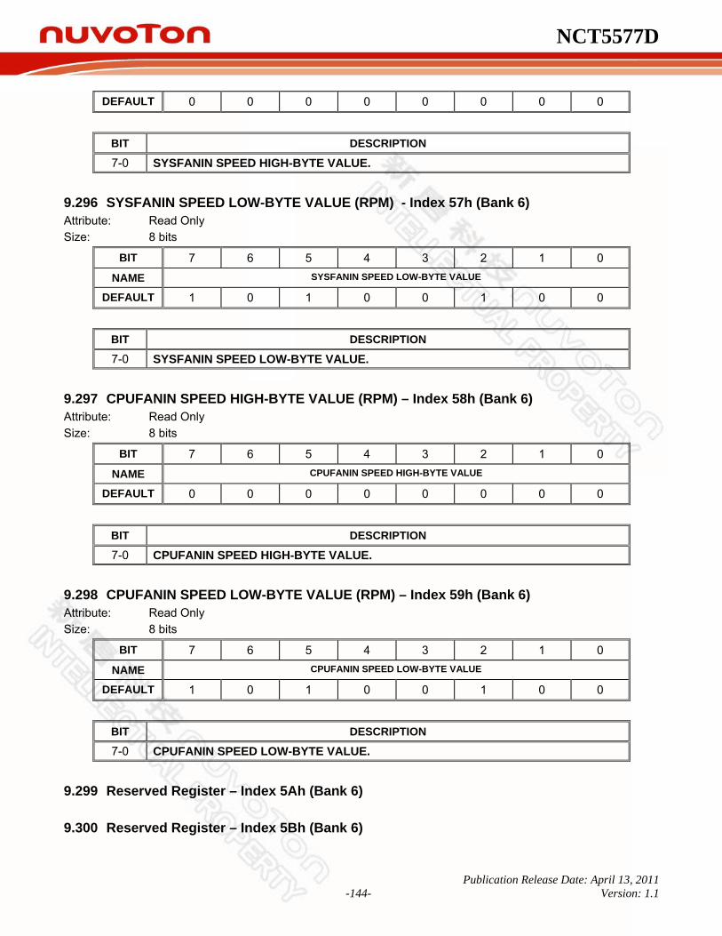
NCT5577D
Publication Release Date: April 13, 2011 -144- Version: 1.1
DEFAULT 0 0 0 0 0 0 0 0
BIT DESCRIPTION
7-0 SYSFANIN SPEED HIGH-BYTE VALUE.
9.296 SYSFANIN SPEED LOW-BYTE VALUE (RPM) - Index 57h (Bank 6) Attribute: Read Only Size: 8 bits
BIT 7 6 5 4 3 2 1 0
NAME SYSFANIN SPEED LOW-BYTE VALUE
DEFAULT 1 0 1 0 0 1 0 0
BIT DESCRIPTION
7-0 SYSFANIN SPEED LOW-BYTE VALUE.
9.297 CPUFANIN SPEED HIGH-BYTE VALUE (RPM) – Index 58h (Bank 6) Attribute: Read Only Size: 8 bits
BIT 7 6 5 4 3 2 1 0
NAME CPUFANIN SPEED HIGH-BYTE VALUE
DEFAULT 0 0 0 0 0 0 0 0
BIT DESCRIPTION
7-0 CPUFANIN SPEED HIGH-BYTE VALUE.
9.298 CPUFANIN SPEED LOW-BYTE VALUE (RPM) – Index 59h (Bank 6) Attribute: Read Only Size: 8 bits
BIT 7 6 5 4 3 2 1 0
NAME CPUFANIN SPEED LOW-BYTE VALUE
DEFAULT 1 0 1 0 0 1 0 0
BIT DESCRIPTION
7-0 CPUFANIN SPEED LOW-BYTE VALUE.
9.299 Reserved Register – Index 5Ah (Bank 6)
9.300 Reserved Register – Index 5Bh (Bank 6)
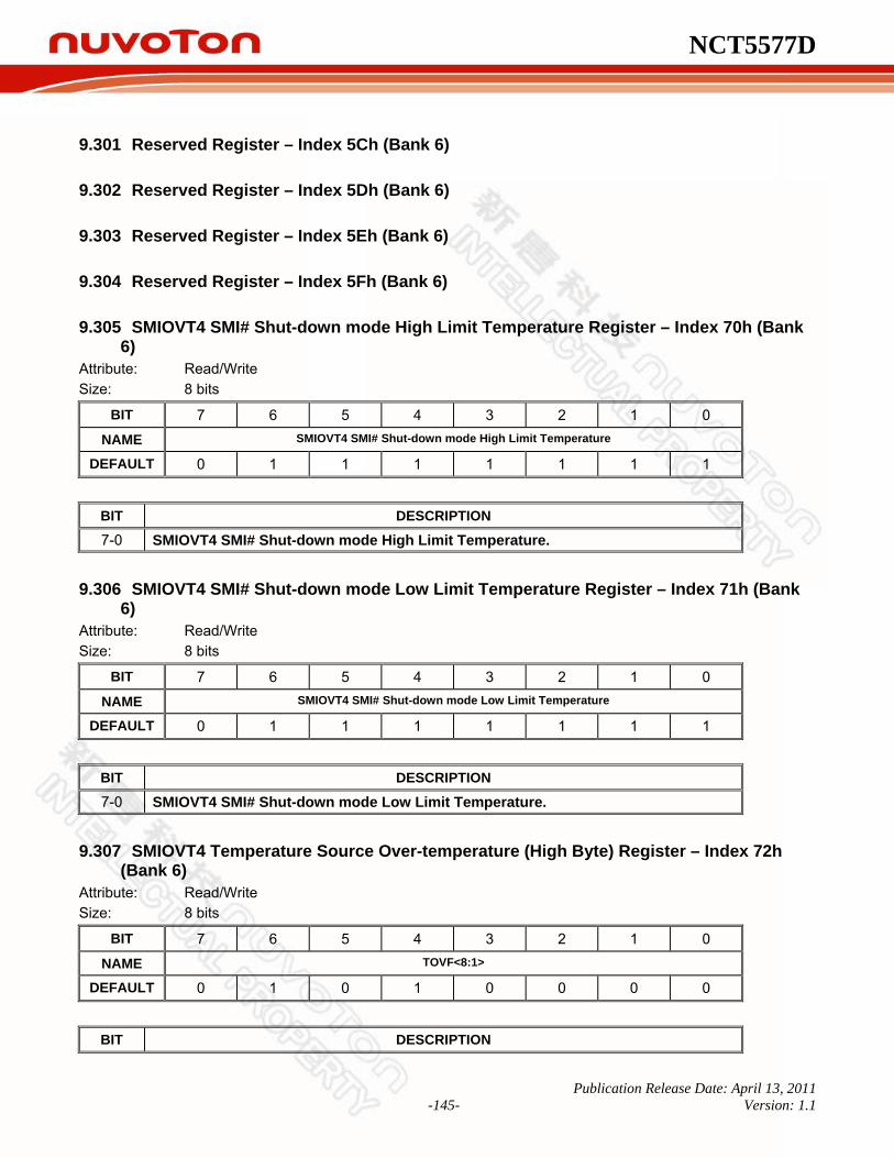
NCT5577D
Publication Release Date: April 13, 2011 -145- Version: 1.1
9.301 Reserved Register – Index 5Ch (Bank 6)
9.302 Reserved Register – Index 5Dh (Bank 6)
9.303 Reserved Register – Index 5Eh (Bank 6)
9.304 Reserved Register – Index 5Fh (Bank 6)
9.305 SMIOVT4 SMI# Shut-down mode High Limit Temperature Register – Index 70h (Bank 6)
Attribute: Read/Write Size: 8 bits
BIT 7 6 5 4 3 2 1 0 NAME SMIOVT4 SMI# Shut-down mode High Limit Temperature
DEFAULT 0 1 1 1 1 1 1 1
BIT DESCRIPTION
7-0 SMIOVT4 SMI# Shut-down mode High Limit Temperature.
9.306 SMIOVT4 SMI# Shut-down mode Low Limit Temperature Register – Index 71h (Bank 6)
Attribute: Read/Write Size: 8 bits
BIT 7 6 5 4 3 2 1 0
NAME SMIOVT4 SMI# Shut-down mode Low Limit Temperature
DEFAULT 0 1 1 1 1 1 1 1
BIT DESCRIPTION
7-0 SMIOVT4 SMI# Shut-down mode Low Limit Temperature.
9.307 SMIOVT4 Temperature Source Over-temperature (High Byte) Register – Index 72h (Bank 6)
Attribute: Read/Write Size: 8 bits
BIT 7 6 5 4 3 2 1 0
NAME TOVF<8:1>
DEFAULT 0 1 0 1 0 0 0 0
BIT DESCRIPTION

NCT5577D
Publication Release Date: April 13, 2011 -146- Version: 1.1
BIT DESCRIPTION
7-0 TOVF<8:1>. Over-temperature bits 8-1. The nine-bit value is in units of 0.5°C, and the default is 80°C.
9.308 SMIOVT4 Temperature Source Hysteresis (High Byte) Register – Index 73h (Bank 6) Attribute: Read/Write Size: 8 bits
BIT 7 6 5 4 3 2 1 0
NAME THYST<8:1>
DEFAULT 0 1 0 0 1 0 1 1
BIT DESCRIPTION
7-0 THYST<8:1>. Hysteresis temperature bits 8-1. The nine-bit value is in units of 0.5°C, and the default is 75°C.
9.309 SMIOVT4 Over-temperature and Hysteresis LSB Temperature and DIS_OVT and EN_WS Register – Index 74h (Bank 6)
Attribute: Read/Write Size: 8 bits
BIT 7 6 5 4 3 2 1 0
NAME TOVF<0> Reserved DIS_OVT_T4 EN_WS_T4 THYST<0>
DEFAULT 0 0 0 0 0 1 0 0
BIT DESCRIPTION
7 TOVF<0>: Over-temperature bits0.
6-3 Reserved
2 DIS_OVT_T4: 0: Enable SMIOVT4 OVT Output 1: Disable SMIOVT4 OVT Output
1 EN_WS_T4 1: SMI# output type of temperature SMIOVT4 temperature is Shut-down Interrupt Mode. 0: SMI# output type is in Shut_down Interrupt Mode. (Default)
0 THYST<0>: Hysteresis temperature bit0.
9.310 SMIOVT5 SMI# Shut-down mode High Limit Temperature Register – Index 75h (Bank 6)
Attribute: Read/Write Size: 8 bits
BIT 7 6 5 4 3 2 1 0 NAME SMIOVT5 SMI# Shut-down mode High Limit Temperature
DEFAULT 0 1 1 1 1 1 1 1
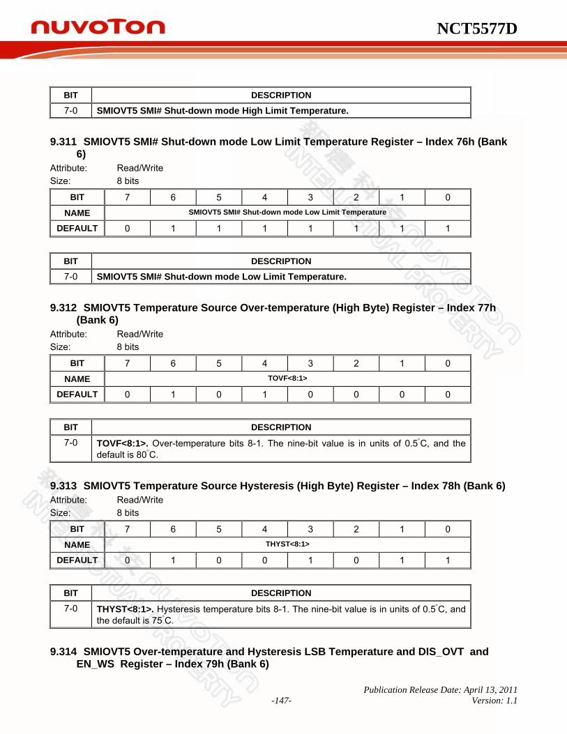
NCT5577D
Publication Release Date: April 13, 2011 -147- Version: 1.1
BIT DESCRIPTION
7-0 SMIOVT5 SMI# Shut-down mode High Limit Temperature.
9.311 SMIOVT5 SMI# Shut-down mode Low Limit Temperature Register – Index 76h (Bank 6)
Attribute: Read/Write Size: 8 bits
BIT 7 6 5 4 3 2 1 0
NAME SMIOVT5 SMI# Shut-down mode Low Limit Temperature
DEFAULT 0 1 1 1 1 1 1 1
BIT DESCRIPTION
7-0 SMIOVT5 SMI# Shut-down mode Low Limit Temperature.
9.312 SMIOVT5 Temperature Source Over-temperature (High Byte) Register – Index 77h (Bank 6)
Attribute: Read/Write Size: 8 bits
BIT 7 6 5 4 3 2 1 0
NAME TOVF<8:1>
DEFAULT 0 1 0 1 0 0 0 0
BIT DESCRIPTION
7-0 TOVF<8:1>. Over-temperature bits 8-1. The nine-bit value is in units of 0.5°C, and the default is 80°C.
9.313 SMIOVT5 Temperature Source Hysteresis (High Byte) Register – Index 78h (Bank 6) Attribute: Read/Write Size: 8 bits
BIT 7 6 5 4 3 2 1 0
NAME THYST<8:1>
DEFAULT 0 1 0 0 1 0 1 1
BIT DESCRIPTION
7-0 THYST<8:1>. Hysteresis temperature bits 8-1. The nine-bit value is in units of 0.5°C, and the default is 75°C.
9.314 SMIOVT5 Over-temperature and Hysteresis LSB Temperature and DIS_OVT and EN_WS Register – Index 79h (Bank 6)

NCT5577D
Publication Release Date: April 13, 2011 -148- Version: 1.1
Attribute: Read/Write Size: 8 bits
BIT 7 6 5 4 3 2 1 0
NAME TOVF<0> Reserved DIS_OVT_T5 EN_WS_T5 THYST<0>
DEFAULT 0 0 0 0 0 1 0 0
BIT DESCRIPTION
7 TOVF<0>: Over-temperature bits0.
6-3 Reserved
2 DIS_OVT_T5: 0: Enable SMIOVT5 OVT Output 1: Disable SMIOVT5 OVT Output
1 EN_WS_T5: 1: SMI# output type of temperature SMIOVT5 temperature is Shut-down Interrupt Mode. 0: SMI# output type is in Shut_down Interrupt Mode. (Default)
0 THYST<0>: Hysteresis temperature bit0.
9.315 SMIOVT6 SMI# Shut-down mode High Limit Temperature Register – Index 7Ah (Bank 6)
Attribute: Read/Write Size: 8 bits
BIT 7 6 5 4 3 2 1 0
NAME SMIOVT6 SMI# Shut-down mode High Limit Temperature
DEFAULT 0 1 1 1 1 1 1 1
BIT DESCRIPTION
7-0 SMIOVT6 SMI# Shut-down mode High Limit Temperature.
9.316 SMIOVT6 SMI# Shut-down mode Low Limit Temperature Register – Index 7Bh (Bank 6)
Attribute: Read/Write Size: 8 bits
BIT 7 6 5 4 3 2 1 0
NAME SMIOVT6 SMI# Shut-down mode Low Limit Temperature
DEFAULT 0 1 1 1 1 1 1 1
BIT DESCRIPTION
7-0 SMIOVT6 SMI# Shut-down mode Low Limit Temperature.
9.317 SMIOVT6 Temperature Source Over-temperature (High Byte) Register – Index 7Ch (Bank 6)

NCT5577D
Publication Release Date: April 13, 2011 -149- Version: 1.1
Attribute: Read/Write Size: 8 bits
BIT 7 6 5 4 3 2 1 0
NAME TOVF<8:1>
DEFAULT 0 1 0 1 0 0 0 0
DESCRIPTION
7-0 TOVF<8:1>. Over-temperature bits 8-1. The nine-bit value is in units of 0.5°C, and the default is 80°C.
9.318 SMIOVT6 Temperature Source Hysteresis (High Byte) Register – Index 7Dh (Bank 6) Attribute: Read/Write Size: 8 bits
BIT 7 6 5 4 3 2 1 0
NAME THYST<8:1>
DEFAULT 0 1 0 0 1 0 1 1
BIT DESCRIPTION
7-0 THYST<8:1>. Hysteresis temperature bits 8-1. The nine-bit value is in units of 0.5°C, and the default is 75°C.
9.319 SMIOVT6 Over-temperature and Hysteresis LSB Temperature and DIS_OVT and EN_WS Register – Index 7Eh (Bank 6)
Attribute: Read/Write Size: 8 bits
BIT 7 6 5 4 3 2 1 0 NAME TOVF<0> Reserved DIS_OVT_T6 EN_WS_T6 THYST<0>
DEFAULT 0 0 0 0 0 1 0 0
BIT DESCRIPTION
7 TOVF<0>: Over-temperature bits0.
6-3 Reserved
2 DIS_OVT_T6: 0: Enable SMIOVT6 OVT Output 1: Disable SMIOVT6 OVT Output
1 EN_WS_T6: 1: SMI# output type of temperature SMIOVT6 temperature is Shut-down Interrupt Mode. 0: SMI# output type is in Shut_down Interrupt Mode. (Default)
0 THYST<0>: Hysteresis temperature bit0.
9.320 Reserved Register – Index 7Fh (Bank 6)
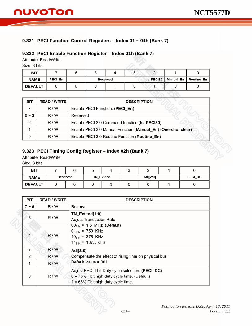
NCT5577D
Publication Release Date: April 13, 2011 -150- Version: 1.1
9.321 PECI Function Control Registers – Index 01 ~ 04h (Bank 7)
9.322 PECI Enable Function Register – Index 01h (Bank 7) Attribute: Read/Write Size: 8 bits
BIT 7 6 5 4 3 2 1 0 NAME PECI_En Reserved Is_PECI30 Manual_En Routine_En
DEFAULT 0 0 0 1 0 1 0 0
BIT READ / WRITE DESCRIPTION
7 R / W Enable PECI Function. (PECI_En)
6 ~ 3 R / W Reserved
2 R / W Enable PECI 3.0 Command function (Is_PECI30)
1 R / W Enable PECI 3.0 Manual Function (Manual_En) (One-shot clear) 0 R / W Enable PECI 3.0 Routine Function (Routine_En)
9.323 PECI Timing Config Register – Index 02h (Bank 7) Attribute: Read/Write Size: 8 bits
BIT 7 6 5 4 3 2 1 0 NAME Reserved TN_Extend Adj[2:0] PECI_DC
DEFAULT 0 0 0 0 0 0 1 0
BIT READ / WRITE DESCRIPTION
7 ~ 6 R / W Reserve
5 R / W
4 R / W
TN_Extend[1:0] Adjust Transaction Rate. 00BIN = 1.5 MHz (Default) 01BIN = 750 KHz 10BIN = 375 KHz 11BIN = 187.5 KHz
3 R / W
2 R / W
1 R / W
Adj[2:0] Compensate the effect of rising time on physical bus Default Value = 001
0 R / W Adjust PECI Tbit Duty cycle selection. (PECI_DC) 0 = 75% Tbit high duty cycle time. (Default) 1 = 68% Tbit high duty cycle time.
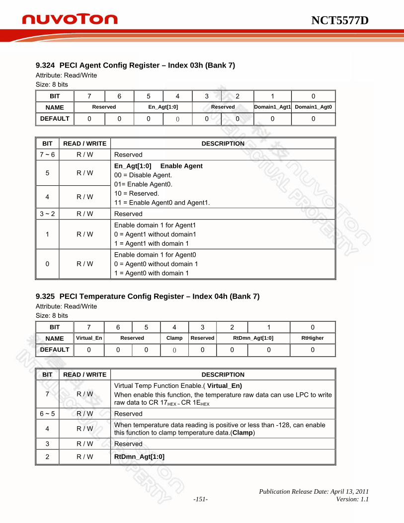
NCT5577D
Publication Release Date: April 13, 2011 -151- Version: 1.1
9.324 PECI Agent Config Register – Index 03h (Bank 7) Attribute: Read/Write Size: 8 bits
BIT 7 6 5 4 3 2 1 0 NAME Reserved En_Agt[1:0] Reserved Domain1_Agt1 Domain1_Agt0
DEFAULT 0 0 0 0 0 0 0 0
BIT READ / WRITE DESCRIPTION
7 ~ 6 R / W Reserved
5 R / W
4 R / W
En_Agt[1:0] Enable Agent 00 = Disable Agent. 01= Enable Agent0. 10 = Reserved. 11 = Enable Agent0 and Agent1.
3 ~ 2 R / W Reserved
1 R / W Enable domain 1 for Agent1 0 = Agent1 without domain1 1 = Agent1 with domain 1
0 R / W Enable domain 1 for Agent0 0 = Agent0 without domain 1 1 = Agent0 with domain 1
9.325 PECI Temperature Config Register – Index 04h (Bank 7) Attribute: Read/Write Size: 8 bits
BIT 7 6 5 4 3 2 1 0 NAME Virtual_En Reserved Clamp Reserved RtDmn_Agt[1:0] RtHigher
DEFAULT 0 0 0 0 0 0 0 0
BIT READ / WRITE DESCRIPTION
7 R / W Virtual Temp Function Enable.( Virtual_En) When enable this function, the temperature raw data can use LPC to write raw data to CR 17HEX ~ CR 1EHEX
6 ~ 5 R / W Reserved
4 R / W When temperature data reading is positive or less than -128, can enable this function to clamp temperature data.(Clamp)
3 R / W Reserved
2 R / W RtDmn_Agt[1:0]

NCT5577D
Publication Release Date: April 13, 2011 -152- Version: 1.1
BIT READ / WRITE DESCRIPTION
1 R / W Agent 1 – Agent 0 always return the relative domain Temperature. 0 = Agent always returns the relative temperature from domain 0. 1 = Agent always returns the relative temperature from domain 1.
0 R / W
Return High Temperature of doamin0 or domain1.(RtHigher) 0 = The temperature of each agent is returned from domain 0 or domain 1, which is controlled by (CR 04HEX)
1 = Return the highest temperature in domain 0 and domain 1 of individual Agent.
9.326 PECI Command Write Date Registers – Index 05 ~ 1Eh (Bank 7)
9.327 PECI Command Address Register – Index 05h (Bank 7) Attribute: Read/Write Size: 8 bits
BIT 7 6 5 4 3 2 1 0
NAME PECI Command Address
DEFAULT 0 0 0 0 0 0 0 0
BIT DESCRIPTION
7~0 The data would be sent to client. Default value is 00HEX.
9.328 PECI Command Write Length Register – Index 06h (Bank 7) Attribute: Read/Write Size: 8 bits
BIT 7 6 5 4 3 2 1 0 NAME PECI Command Write Length
DEFAULT 0 0 0 0 0 0 0 0
BIT DESCRIPTION
7~0 The data would be sent to client. Default value is 00HEX.
9.329 PECI Command Read Length Register – Index 07h (Bank 7) Attribute: Read/Write Size: 8 bits
BIT 7 6 5 4 3 2 1 0
NAME PECI Command Read Length
DEFAULT 0 0 0 0 0 0 0 0
BIT DESCRIPTION

NCT5577D
Publication Release Date: April 13, 2011 -153- Version: 1.1
BIT DESCRIPTION
7~0 The data would be sent to client. Default value is 00HEX.
9.330 PECI Command Code Register – Index 08h (Bank 7) Attribute: Read/Write Size: 8 bits
BIT 7 6 5 4 3 2 1 0
NAME PECI Command Code
DEFAULT 0 0 0 0 0 0 0 0
BIT DESCRIPTION
7~0 The data would be sent to client. Default value is 00HEX.
9.331 PECI Command Tbase0 Register – Index 09h (Bank 7) Attribute: Read/Write Size: 8 bits
BIT 7 6 5 4 3 2 1 0 NAME Reserved Tbase 0
DEFAULT 0 0 0 0 0 0 0 0
BIT DESCRIPTION
7~0 The data would be sent to client. Default value is 00HEX.
9.332 PECI Command Tbase1 Register – Index 0Ah (Bank 7) Attribute: Read/Write Size: 8 bits
BIT 7 6 5 4 3 2 1 0
NAME Reserved Tbase 1
DEFAULT 0 0 0 0 0 0 0 0
BIT DESCRIPTION
7~0 The data would be sent to client. Default value is 00HEX.
9.333 PECI Command Write Data 1 Register – Index 0Bh (Bank 7) Attribute: Read/Write Size: 8 bits
BIT 7 6 5 4 3 2 1 0
NAME PECI Write Data 1
DEFAULT 0 0 0 0 0 0 0 0

NCT5577D
Publication Release Date: April 13, 2011 -154- Version: 1.1
BIT DESCRIPTION
7~0 The data would be sent to client. Default value is 00HEX.
9.334 PECI Command Write Data 2 Register – Index 0Ch (Bank 7) Attribute: Read/Write Size: 8 bits
BIT 7 6 5 4 3 2 1 0
NAME PECI Write Data 2
DEFAULT 0 0 0 0 0 0 0 0
BIT DESCRIPTION
7~0 The data would be sent to client. Default value is 00HEX.
9.335 PECI Command Write Data 3 Register – Index 0Dh (Bank 7) Attribute: Read/Write Size: 8 bits
BIT 7 6 5 4 3 2 1 0
NAME PECI Write Data 3
DEFAULT 0 0 0 0 0 0 0 0
BIT DESCRIPTION
7~0 The data would be sent to client. Default value is 00HEX.
9.336 PECI Command Write Data 4 Register – Index 0Eh (Bank 7) Attribute: Read/Write Size: 8 bits
BIT 7 6 5 4 3 2 1 0
NAME PECI Write Data 4
DEFAULT 0 0 0 0 0 0 0 0
BIT DESCRIPTION
7~0 The data would be sent to client. Default value is 00HEX.
9.337 PECI Command Write Data 5 Register – Index 0Fh (Bank 7) Attribute: Read/Write Size: 8 bits

NCT5577D
Publication Release Date: April 13, 2011 -155- Version: 1.1
BIT 7 6 5 4 3 2 1 0
NAME PECI Write Data 5
DEFAULT 0 0 0 0 0 0 0 0
BIT DESCRIPTION
7~0 The data would be sent to client. Default value is 00HEX.
9.338 PECI Command Write Data 6 Register – Index 10h (Bank 7) Attribute: Read/Write Size: 8 bits
BIT 7 6 5 4 3 2 1 0
NAME PECI Write Data 6
DEFAULT 0 0 0 0 0 0 0 0
BIT DESCRIPTION
7~0 The data would be sent to client. Default value is 00HEX.
9.339 PECI Command Write Data 7 Register – Index 11h (Bank 7) Attribute: Read/Write Size: 8 bits
BIT 7 6 5 4 3 2 1 0
NAME PECI Write Data 7
DEFAULT 0 0 0 0 0 0 0 0
BIT DESCRIPTION
7~0 The data would be sent to client. Default value is 00HEX.
9.340 PECI Command Write Data 8 Register – Index 12h (Bank 7) Attribute: Read/Write Size: 8 bits
BIT 7 6 5 4 3 2 1 0
NAME PECI Write Data 8
DEFAULT 0 0 0 0 0 0 0 0
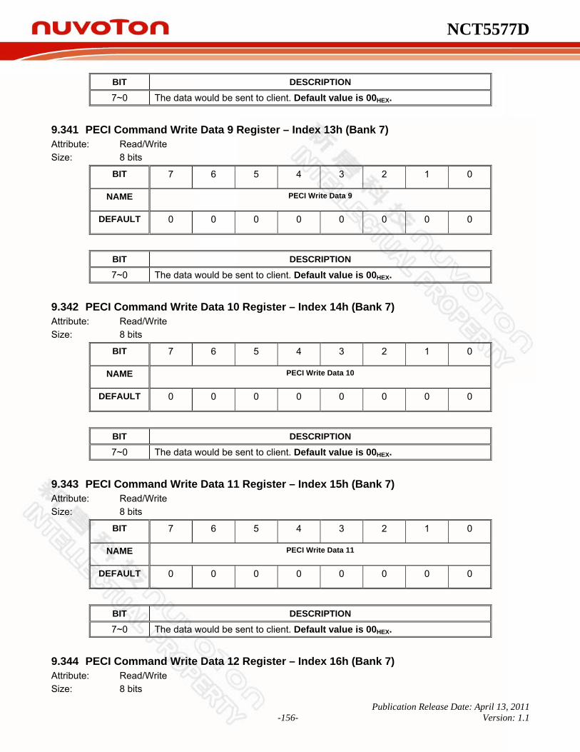
NCT5577D
Publication Release Date: April 13, 2011 -156- Version: 1.1
BIT DESCRIPTION
7~0 The data would be sent to client. Default value is 00HEX.
9.341 PECI Command Write Data 9 Register – Index 13h (Bank 7) Attribute: Read/Write Size: 8 bits
BIT 7 6 5 4 3 2 1 0
NAME PECI Write Data 9
DEFAULT 0 0 0 0 0 0 0 0
BIT DESCRIPTION
7~0 The data would be sent to client. Default value is 00HEX.
9.342 PECI Command Write Data 10 Register – Index 14h (Bank 7) Attribute: Read/Write Size: 8 bits
BIT 7 6 5 4 3 2 1 0
NAME PECI Write Data 10
DEFAULT 0 0 0 0 0 0 0 0
BIT DESCRIPTION
7~0 The data would be sent to client. Default value is 00HEX.
9.343 PECI Command Write Data 11 Register – Index 15h (Bank 7) Attribute: Read/Write Size: 8 bits
BIT 7 6 5 4 3 2 1 0
NAME PECI Write Data 11
DEFAULT 0 0 0 0 0 0 0 0
BIT DESCRIPTION
7~0 The data would be sent to client. Default value is 00HEX.
9.344 PECI Command Write Data 12 Register – Index 16h (Bank 7) Attribute: Read/Write Size: 8 bits

NCT5577D
Publication Release Date: April 13, 2011 -157- Version: 1.1
BIT 7 6 5 4 3 2 1 0
NAME PECI Write Data 12
DEFAULT 0 0 0 0 0 0 0 0
BIT DESCRIPTION
7~0 The data would be sent to client. Default value is 00HEX.
9.345 PECI Agent Relative Temperature Register – Index 17h-1Eh (Bank 7) These registers return the raw data retrieved from PECI GetTemp(). The data may be the error code (range: 8000H~81FFH) or relative temperatures to process the defined Tbase. The error code will only be update in ARTR and absolute Temperature will not be updated when the error code is received. If the RtHigher mechanism is activated, the normal temperature will always be returned first. In case both 2 domains return errors, the return priority will be Overflow Error > Underflow Error > Missing Diode > General Error. The reset value is 8001HEX, in that PECI is defaulted to be off. In PECI, 8001HEX means the diode is missing. Attribute: Read / Write(When Virtual_En enable)
ADDRESS 17-1E DESCRIPTION
17h[15:8],18h[7:0] Domain0 Relative Temperature Agent0 [15:0]
19h[15:8],1Ah[7:0] Domain1 Relative Temperature Agent0 [15:0]
1Bh[15:8],1Ch[7:0] Domain0 Relative Temperature Agent1 [15:0]
1Dh[15:8],1Eh[7:0] Domain1 Relative Temperature Agent1 [15:0]
GetTemp() PECI Temperature format:
BIT DESCRIPTION
15 Sign Bit. (Sign) In PECI Protocol, this bit should always be 1 to represent a negative temperature.
14-6 The integer part of the relative temperature. (Temperature[8:0]) 5 TEMP_2. 0.5℃ unit.
4 TEMP_4. 0.25℃ unit.
3 TEMP_8. 0.125℃ unit.
2 TEMP_16. 0.0625℃ unit.
1 TEMP_32. 0.03125℃ unit.
0 TEMP_64. 0.015625℃ unit.
GetTemp() Response Definition:
RESPONSE MEANING
General Sensor Error (GSE)
Thermal scan did not complete in time. Retry is appropriate.
0x0000 Processor is running at its maximum temperature or is currently being reset.

NCT5577D
Publication Release Date: April 13, 2011 -158- Version: 1.1
All other data Valid temperature reading, reported as a negative offset from the TCC activation temperature. The valide temperature reading is referred to GetTemp() PECI Temperature format
Error Code
Description Host operation
8000HEX General Sensor Error
8001HEX Sensing Device Missing
No further processing.
8002HEX Operational, but the temperature is lower than the sensor operation range.
Compulsorily write 0℃ back to the temperature readouts.
8003HEX Operational, but the temperature is higher than the sensor operation range.
Compulsorily write 127℃ back to the temperature readouts.
8004HEX
≀
81FFHEX
Reserved. No further operation.
9.346 PECI Command Read Date Registers – Index 1F ~ 32h (Bank 7)
9.347 PECI Alive Agent Register – Index 1Fh (Bank 7) Attribute: Read only Size: 8 bits Record which agentis able to respond to Ping().Default value is 00HEX. 1: agent is able to respond to Ping() command. Agent alive 0: agent isn’t able to respond to Ping() command. Agent is not alive
BIT 7 6 5 4 3 2 1 0
NAME Reserved PECI Alive Agent
DEFAULT 0 0 0 0 0 0 0 0
BIT DESCRIPTION
7~4 Reserve 3 1: agent3 is able to respond to Ping() command. Agent alive
0: agent3 isn’t able to respond to Ping() command. Agent is not alive
2 1: agent2 is able to respond to Ping() command. Agent alive 0: agent2 isn’t able to respond to Ping() command. Agent is not alive
1 1: agent1 is able to respond to Ping() command. Agent alive 0: agent1 isn’t able to respond to Ping() command. Agent is not alive
0 1: agent0 is able to respond to Ping() command. Agent alive 0: agent0 isn’t able to respond to Ping() command. Agent is not alive

NCT5577D
Publication Release Date: April 13, 2011 -159- Version: 1.1
9.348 PECI Temperature Reading Register (Integer) – Index 20h (Bank 7) Attribute: Read only Size: 8 bits
BIT 7 6 5 4 3 2 1 0
NAME PECI Temperature Reading---Integer [9:2]
DEFAULT 0 0 1 0 1 0 0 0
BIT DESCRIPTION
7~0 Temperature value [9] (Sign bit) Temperature value [8:2] (Integer bits) Temperature value [1:0] (Fraction bits)
Note. Temperature reading register is count from raw data and Tbase, for example:
Raw data + Tbase = Temp Reading
Bank7, Index [17][18] + Bank7, Index [09] = Bank7, Index [20][21]
9.349 PECI Temperature Reading Register (Fraction) – Index 21h (Bank 7) Attribute: Read only Size: 8 bits
BIT 7 6 5 4 3 2 1 0
NAME Reserved PECI Temperature Vaule[1:0]
DEFAULT 0 0 0 0 0 0 0 0
BIT DESCRIPTION
7~0 Temperature value [9] (Sign bit) Temperature value [8:2] (Integer bits) Temperature value [1:0] (Fraction bits)
9.350 PECI Command TN Count Value Register – Index 22h (Bank 7) Attribute: Read only Size: 8 bits
BIT 7 6 5 4 3 2 1 0
NAME PECI Timing Negotiation count Value[7:0]
DEFAULT 0 0 0 0 0 0 0 0

NCT5577D
Publication Release Date: April 13, 2011 -160- Version: 1.1
BIT DESCRIPTION
7~0 The data would be get from client. Default value is 00HEX.
9.351 PECI Command TN Count Value Register – Index 23h (Bank 7) Attribute: Read only Size: 8 bits
BIT 7 6 5 4 3 2 1 0
NAME Reserved PECI Timing Negotiation count Value[11:8]
DEFAULT 0 0 0 0 0 0 0 0
BIT DESCRIPTION
7~0 The data would be get from client. Default value is 00HEX.
9.352 PECI Command Warning Flag Register – Index 24h (Bank 7) Attribute: Read only Size: 8 bits
BIT 7 6 5 4 3 2 1 0
NAME Reserved Alert Value[3:0]
DEFAULT 0 0 0 0 0 0 0 0
BIT DESCRIPTION
7~0 Agent Alert Bit (Default value is 0) 0: Agent has valid FCS. 1: Agent has invalid FCS in the previous 3 transactions. Default value is 00HEX.
9.353 PECI Command FCS Data Register – Index 25h (Bank 7) Attribute: Read only Size: 8 bits
BIT 7 6 5 4 3 2 1 0
NAME Reserve Wraning CC_Fail ZeroWFCS AbortWFCS BadRFCS BadWFCS
DEFAULT 0 0 0 0 0 0 0 0
BIT DESCRIPTION
7~0 Retrieve PECI related data from client and host. Default value is 00HEX.
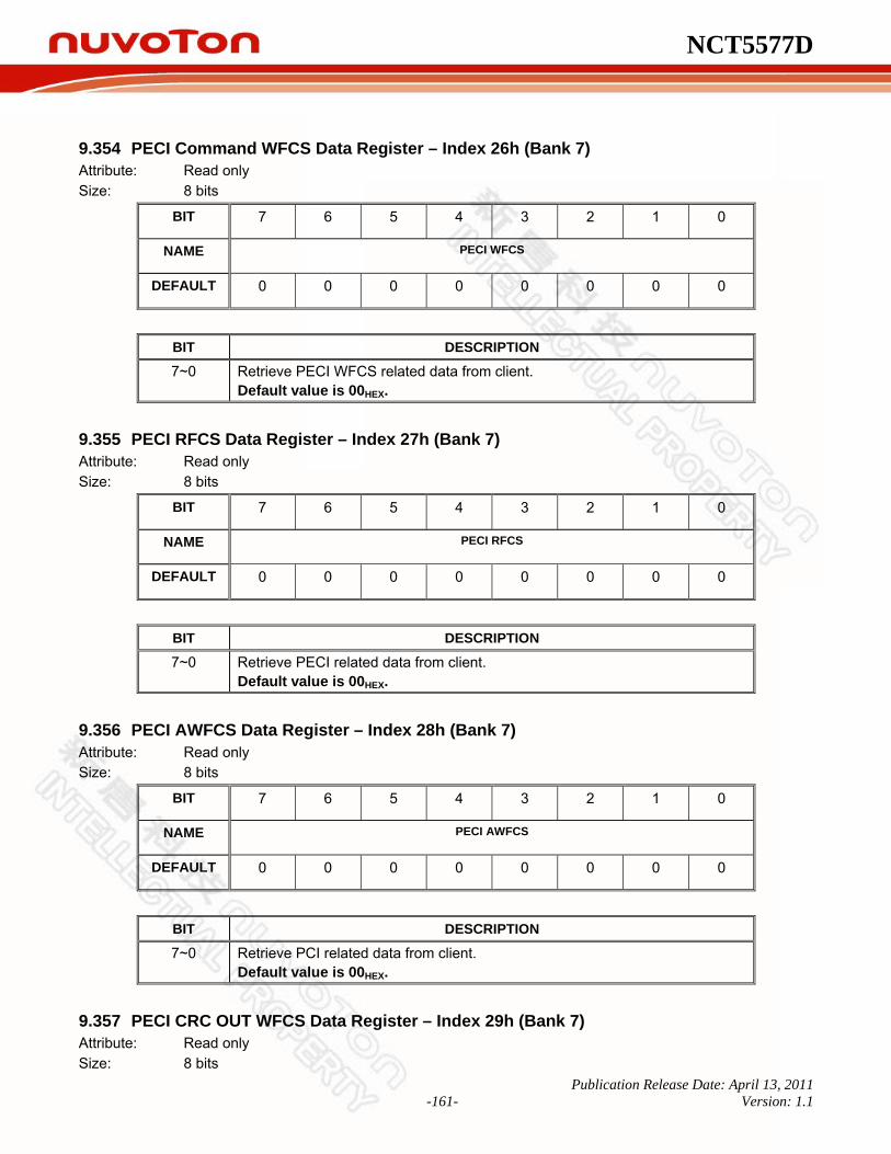
NCT5577D
Publication Release Date: April 13, 2011 -161- Version: 1.1
9.354 PECI Command WFCS Data Register – Index 26h (Bank 7) Attribute: Read only Size: 8 bits
BIT 7 6 5 4 3 2 1 0
NAME PECI WFCS
DEFAULT 0 0 0 0 0 0 0 0
BIT DESCRIPTION
7~0 Retrieve PECI WFCS related data from client. Default value is 00HEX.
9.355 PECI RFCS Data Register – Index 27h (Bank 7) Attribute: Read only Size: 8 bits
BIT 7 6 5 4 3 2 1 0
NAME PECI RFCS
DEFAULT 0 0 0 0 0 0 0 0
BIT DESCRIPTION
7~0 Retrieve PECI related data from client. Default value is 00HEX.
9.356 PECI AWFCS Data Register – Index 28h (Bank 7) Attribute: Read only Size: 8 bits
BIT 7 6 5 4 3 2 1 0
NAME PECI AWFCS
DEFAULT 0 0 0 0 0 0 0 0
BIT DESCRIPTION
7~0 Retrieve PCI related data from client. Default value is 00HEX.
9.357 PECI CRC OUT WFCS Data Register – Index 29h (Bank 7) Attribute: Read only Size: 8 bits

NCT5577D
Publication Release Date: April 13, 2011 -162- Version: 1.1
BIT 7 6 5 4 3 2 1 0
NAME PECI CRC OUT WFCS
DEFAULT 0 0 0 0 0 0 0 0
BIT DESCRIPTION
7~0 Retrieve PECI related data from client. Default value is 00HEX.
9.358 PECI Command Read Data 1 Register – Index 2Ah (Bank 7) Attribute: Read/Write Size: 8 bits
BIT 7 6 5 4 3 2 1 0
NAME PECI Read Data 1
DEFAULT 0 0 0 0 0 0 0 0
BIT DESCRIPTION
7~0 The data would be get from client. Default value is 00HEX.
9.359 PECI Command Read Data 2 Register – Index 2Bh (Bank 7) Attribute: Read/Write Size: 8 bits
BIT 7 6 5 4 3 2 1 0
NAME PECI Read Data 2
DEFAULT 0 0 0 0 0 0 0 0
BIT DESCRIPTION
7~0 The data would be get from client. Default value is 00HEX.
9.360 PECI Command Read Data 3 Register – Index 2Ch (Bank 7) Attribute: Read/Write Size: 8 bits
BIT 7 6 5 4 3 2 1 0
NAME PECI Read Data 3
DEFAULT 0 0 0 0 0 0 0 0
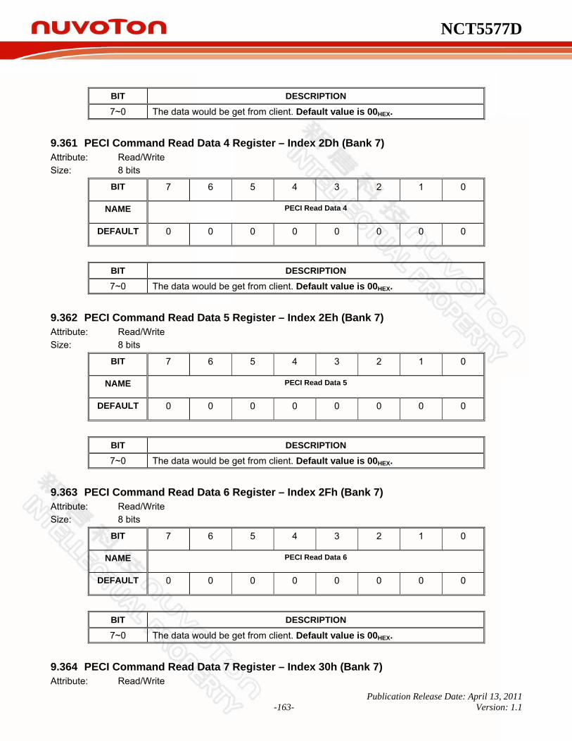
NCT5577D
Publication Release Date: April 13, 2011 -163- Version: 1.1
BIT DESCRIPTION
7~0 The data would be get from client. Default value is 00HEX.
9.361 PECI Command Read Data 4 Register – Index 2Dh (Bank 7) Attribute: Read/Write Size: 8 bits
BIT 7 6 5 4 3 2 1 0
NAME PECI Read Data 4
DEFAULT 0 0 0 0 0 0 0 0
BIT DESCRIPTION
7~0 The data would be get from client. Default value is 00HEX.
9.362 PECI Command Read Data 5 Register – Index 2Eh (Bank 7) Attribute: Read/Write Size: 8 bits
BIT 7 6 5 4 3 2 1 0
NAME PECI Read Data 5
DEFAULT 0 0 0 0 0 0 0 0
BIT DESCRIPTION
7~0 The data would be get from client. Default value is 00HEX.
9.363 PECI Command Read Data 6 Register – Index 2Fh (Bank 7) Attribute: Read/Write Size: 8 bits
BIT 7 6 5 4 3 2 1 0
NAME PECI Read Data 6
DEFAULT 0 0 0 0 0 0 0 0
BIT DESCRIPTION
7~0 The data would be get from client. Default value is 00HEX.
9.364 PECI Command Read Data 7 Register – Index 30h (Bank 7) Attribute: Read/Write
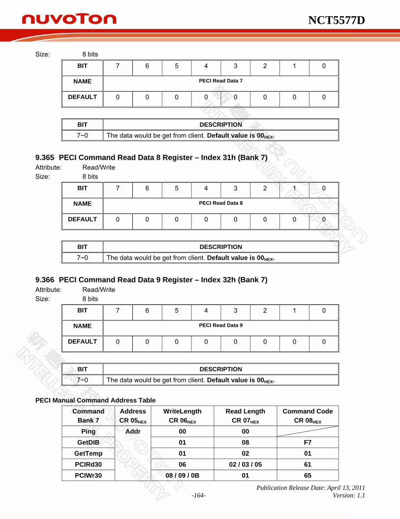
NCT5577D
Publication Release Date: April 13, 2011 -164- Version: 1.1
Size: 8 bits
BIT 7 6 5 4 3 2 1 0
NAME PECI Read Data 7
DEFAULT 0 0 0 0 0 0 0 0
BIT DESCRIPTION
7~0 The data would be get from client. Default value is 00HEX.
9.365 PECI Command Read Data 8 Register – Index 31h (Bank 7) Attribute: Read/Write Size: 8 bits
BIT 7 6 5 4 3 2 1 0
NAME PECI Read Data 8
DEFAULT 0 0 0 0 0 0 0 0
BIT DESCRIPTION
7~0 The data would be get from client. Default value is 00HEX.
9.366 PECI Command Read Data 9 Register – Index 32h (Bank 7) Attribute: Read/Write Size: 8 bits
BIT 7 6 5 4 3 2 1 0
NAME PECI Read Data 9
DEFAULT 0 0 0 0 0 0 0 0
BIT DESCRIPTION
7~0 The data would be get from client. Default value is 00HEX. PECI Manual Command Address Table
Command Bank 7
Address CR 05HEX
WriteLength CR 06HEX
Read Length CR 07HEX
Command CodeCR 08HEX
Ping 00 00 GetDIB 01 08 F7
GetTemp 01 02 01 PCIRd30 06 02 / 03 / 05 61 PCIWr30
Addr
08 / 09 / 0B 01 65

NCT5577D
Publication Release Date: April 13, 2011 -165- Version: 1.1
PCIRdLocal30 05 02 / 03 / 05 E1 PCIWrLocal30 07 / 08 / 0A 01 E5
PKGRd30 05 02 / 03 / 05 A1 PKGWr30 07 / 08 / 0A 01 A5
IAMSRRd30 05 02 / 03 / 05 / 09 B1 IAMSRWr30 07 / 08 / 0A / 0E 01 B5
PECI Manual Command Read Data Table
Command PCI Rd30
PCI Wr30
PCIRd Local30
PCIWrLocal30
PKG Rd30
PKG Wr30
IAMSR Rd30
IAMSR Wr30 GetDIB GetTemp
Command Code 61 65 E1 E5 A1 A5 B1 B5 F7 01
RdData 1 CR 2AHEX
Ccode Ccode Ccode Ccode Ccode Ccode Ccode Ccode X X
RdData 2 CR 2BHEX
X X X X X X Data
LSB_1X
Device Info
X
RdData 3 CR 2CHEX
X X X X X X Data
LSB_2X
RevisionNumber
X
RdData 4 CR 2DHEX
X X X X X X Data
LSB_3X
Reserved1
X
RdData 5 CR 2EHEX
X X x X X X Data
LSB_4X
Reserved2
X
RdData 6 CR 2FHEX
Data LSB_1
X Data
LSB_1 X
Data LSB_1
X Data
LSB_5X
Reserved3
X
RdData 7 CR 30HEX
Data LSB_2
X Data
LSB_2 X
Data LSB_2
X Data
LSB_6X
Reserved4
X
RdData 8 CR 31HEX
Data LSB_3
X Data
LSB_3 X
Data LSB_3
X Data
LSB_7X
Reserved5
Temp_LB
RdData 9 CR 32HEX
Data MSB
x Data MSB
X Data MSB
X Data MSB
X Reserved
6 Temp_HB
PECI Manual Command Write Data Table
Command PCI Rd30
PCI Wr30
PCIRd Local30
PCIWrLocal30
PKG Rd30
PKG Wr30
IAMSR Rd30
IAMSRWr30
Command Code 61 65 E1 E5 A1 A5 B1 B5
WrData 1 CR 0BHEX
Host ID
Host ID
Host ID
Host ID
Host ID
Host ID
Host ID
Host ID
WrData 2 CR 0CHEX
Addr LSB_1
Addr LSB_1
Addr LSB_1
Addr LSB_1
Index Index Process
or ID
Processor ID
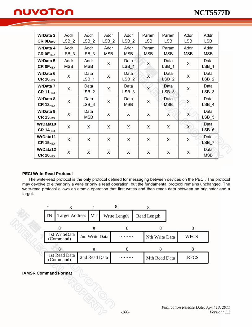
NCT5577D
Publication Release Date: April 13, 2011 -166- Version: 1.1
WrData 3 CR 0DHEX
Addr LSB_2
Addr LSB_2
Addr LSB_2
Addr LSB_2
Param LSB
Param LSB
Addr LSB
Addr LSB
WrData 4 CR 0EHEX
Addr LSB_3
Addr LSB_3
Addr MSB
Addr MSB
Param MSB
Param MSB
Addr MSB
Addr MSB
WrData 5 CR 0FHEX
Addr MSB
Addr MSB
X Data
LSB_1X
Data LSB_1
X Data
LSB_1 WrData 6 CR 10HEX X
Data LSB_1
X Data
LSB_2X
Data LSB_2
X Data
LSB_2 WrData 7 CR 11HEX
X Data
LSB_2 X
Data LSB_3
X Data
LSB_3 X
Data LSB_3
WrData 8 CR 12HEX
X Data
LSB_3 X
Data MSB
X Data MSB
X Data
LSB_4 WrData 9 CR 13HEX X
Data MSB
X X X X X Data
LSB_5 WrData10 CR 14HEX
X X X X X X X Data
LSB_6 WrData11 CR 15HEX
X X X X X X X Data
LSB_7 WrData12 CR 16HEX
X X X X X X X Data MSB
PECI Write-Read Protocol
The write-read protocol is the only protocol defined for messaging between devices on the PECI. The protocol may devolve to either only a write or only a read operation, but the fundamental protocol remains unchanged. The write-read protocol allows an atomic operation that first writes and then reads data between an originator and a target.
2
TN
8
Target Address
1
MT Write Length Read Length
8 81st WriteData
8
WFCS(Command) 2nd Write Data ………
8
Nth Write Data
8 8
8
8 81st Read Data
8
RFCS(Command) 2nd Read Data ………
8
Mth Read Data
8
IAMSR Command Format

NCT5577D
Publication Release Date: April 13, 2011 -167- Version: 1.1
2
TN
8
Client Address1
MT Write Length Read Length
8 8Cmd Code
8
WFCS(0xb1)Host ID[7:1]&
Retry[0] Processor ID
8
MSR Address
8 8
8
8 8Completion
Code
8
LSB7
8 8
(0x30) (0x05) (0x09)
8
LSB MSB
8 88
RFCS
8
MSB
LSB6 LSB5 LSB4 LSB3
LSB2 LSB1
Example:
2
TN
8
Client Address1
MT Write Length Read Length
8 8Cmd Code
8WFCS
CR 08HEX
Wr Data 18
8 8
8
8 8Rd Data 1
8 8 8
CR 05HEX CR 06HEX CR 07HEX
8
8 88
RFCS
8
Wr Data 2 Wr Data 3 Wr Data 4
Rd Data 2 Rd Data 3 Rd Data 4 Rd Data 5 Rd Data 6
Rd Data 7 Rd Data 8 Rd Data 9
CR 0BHEX CR 0CHEX CR 0DHEX CR 0EHEX
CR 2AHEX CR 2BHEX CR 2CHEX CR 2DHEX CR 2EHEX CR 2FHEX
CR 30HEX CR 31HEX CR 32HEX

NCT5577D
Publication Release Date: April 13, 2011 -168- Version: 1.1
10. UART PORT
10.1 UART Control Register (UCR) (Read/Write) The UART Control Register defines and controls the protocol for asynchronous data communications, including data length, stop bit, parity, and baud rate selection.
BIT 7 6 5 4 3 2 1 0
NAME BDLAB SSE PBFE EPE PBE MSBE DLS1 DLS0
DEFAULT 0 0 0 0 0 0 0 0
BIT DESCRIPTION
7
BDLAB (Baud Rate Divisor Latch Access Bit). When this bit is set to logic 1, designers can access the divisor (in 16-bit binary format) from the divisor latches of the baud-rate generator during a read or write operation. When this bit is set to logic 0, the Receiver Buffer Register, the Transmitter Buffer Register, and the Interrupt Control Register can be accessed.
6 SSE (Set Silence Enable). A logic 1 forces the Serial Output (SOUT) to a silent state (a logical 0). Only IRTX is affected by this bit; the transmitter is not affected.
5 PBFE (Parity Bit Fixed Enable). When PBE and PBFE of UCR are both set to logic 1, (1) if EPE is logic 1, the parity bit is logical 0 when transmitting and checking; (2) if EPE is logic 0, the parity bit is logical 1 when transmitting and checking.
4
EPE (Even Parity Enable). When PBE is set to logic 1, this bit counts the number of logic 1’s in the data word bits and determines the parity bit. When this bit is set to logic 1, the parity bit is set to logic 1 if an even number of logic 1’s are sent or checked. When the bit is set to logic 0, the parity bit is logic 1, if an odd number of logic 1’s are sent or checked.
3 PBE (Parity Bit Enable). When this bit is set to logic 1, the transmitter inserts a stop bit between the last data bit and the stop bit of the SOUT, and the receiver checks the parity bit in the same position.
2
MSBE (Multiple Stop Bit Enable). Defines the number of stop bits in each serial character that is transmitted or received. (1) If MSBE is set to logic 0, one stop bit is sent and checked. (2) If MSBE is set to logic 1 and the data length is 5 bits, one-and-a-half stop bits
are sent and checked. (3) If MSBE is set to logic 1 and the data length is 6, 7, or 8 bits, two stop bits are
sent and checked.
1 DLS1 (Data Length Select Bit 1). Defines the number of data bits that are sent or checked in each serial character.
0 DLS0 (Data Length Select Bit 0). Defines the number of data bits that are sent or checked in each serial character.
DLS1 DLS0 DATA LENGTH
0 0 5 bits
0 1 6 bits
1 0 7 bits

NCT5577D
Publication Release Date: April 13, 2011 -169- Version: 1.1
DLS1 DLS0 DATA LENGTH
1 1 8 bits
The following table identifies the remaining UART registers. Each one is described separately in the following sections.
Table 10-1 Register Summary for UART
Bit Number Register Address Base 0 1 2 3 4 5 6 7
+ 0 BDLAB = 0
Receiver Buffer
Register (Read Only)
RBR RX Data Bit 0
RX DataBit 1
RX Data Bit 2
RX Data Bit 3
RX Data Bit 4
RX Data Bit 5
RX DataBit 6
RX DataBit 7
+ 0 BDLAB = 0
Transmitter Buffer Register
(Write Only)
TBR TX Data Bit 0
TX Data Bit 1
TX Data Bit 2
TX Data Bit 3
TX Data Bit 4
TX Data Bit 5
TX Data Bit 6
TX Data Bit 7
+ 1 BDLAB = 0
Interrupt Control Register
ICR RBR Data Ready
Interrupt Enable
(ERDRI)
TBR Empty
Interrupt Enable
(ETBREI)
USR Interrupt Enable
(EUSRI)
HSR Interrupt Enable
(EHSRI)
0 0 0 0
+ 2 Interrupt Status Register
(Read Only)
ISR “0” if Interrupt Pending
Interrupt Status Bit (0)
Interrupt Status Bit (1)
Interrupt Status
Bit (2)**
0 0 FIFOs Enabled
**
FIFOs Enabled
** + 2 UART FIFO
Control Register
(Write Only)
UFR FIFO Enable
RCVR FIFO Reset
XMIT FIFO Reset
DMA Mode Select
Reserved Reversed RX Interrupt
Active Level(LSB)
RX Interrupt
Active Level(MSB)
+ 3 UART Control Register
UCR Data Length Select Bit 0
(DLS0)
Data Length Select Bit 1
(DLS1)
Multiple Stop Bits Enable (MSBE)
Parity Bit
Enable (PBE)
Even Parity
Enable (EPE)
Parity Bit Fixed Enable PBFE)
Set Silence Enable (SSE)
Baudrate Divisor Latch
Access Bit(BDLAB)
+ 4 Handshake Control Register
HCR Data Terminal Ready (DTR)
Request to
Send (RTS)
LoopbackRI
Input
IRQ Enable
Internal Loopback
Enable
0 0 0
+ 5 UART Status Register
USR RBR Data Ready (RDR)
Overrun Error
(OER)
Parity BitError
(PBER)
No Stop Bit
Error (NSER)
Silent Byte
Detected(SBD)
TBR Empty (TBRE)
TSR Empty (TSRE)
RX FIFO Error
Indication (RFEI) **
+ 6 Handshake Status Register
HSR CTS Toggling (TCTS)
DSR Toggling (TDSR)
RI Falling Edge
(FERI)
DCD Toggling (TDCD)
Clear to Send (CTS)
Data Set Ready (DSR)
Ring Indicator
(RI)
Data CarrierDetect (DCD)
+ 7 User Defined Register
UDR Bit 0 Bit 1 Bit 2 Bit 3 Bit 4 Bit 5 Bit 6 Bit 7
+ 0 BDLAB = 1
Baudrate Divisor Latch
Low
BLL Bit 0 Bit 1 Bit 2 Bit 3 Bit 4 Bit 5 Bit 6 Bit 7
+ 1 BDLAB = 1
Baudrate Divisor Latch
High
BHL Bit 8 Bit 9 Bit 10 Bit 11 Bit 12 Bit 13 Bit 14 Bit 15
*: Bit 0 is the least significant bit. The least significant bit is the first bit serially transmitted or received. **: These bits are always 0 in 16450 Mode.

NCT5577D
Publication Release Date: April 13, 2011 -170- Version: 1.1
10.2 UART Status Register (USR) (Read/Write) This 8-bit register provides information about the status of data transfer during communication.
BIT 7 6 5 4 3 2 1 0
NAME RF EI TSRE TBRE SBD NSER PBER OER RDR
DEFAULT 0 1 1 0 0 0 0 0
BIT DESCRIPTION
7
RF EI (RX FIFO Error Indication). In 16450 mode, this bit is always set to logical 0. in 16550 mode, this bit is set to logical 1 when there is at least one parity-bit error and no stop0bit error or silent-byte detected in the FIFO. In 16550 mode, this bit is cleared to logical 0 by reading from the USR if there are no remaining errors left in the FIFO.
6 TSRE (Transmitter Shift Register Empty). In 16450 mode, this bit is set to logical 1 when TBR and TSR are both empty. In 16550 mode, it is set to logical 1 when the transmit FIFO and TSR are both empty. Otherwise, this bit is set to logical 0.
5
TBRE (Transmitter Buffer Register Empty). In 16450 mode, when a data character is transferred from TBR to TSR, this bit is set to logical 1. If ETREI of ICR is high, and interrupt is generated to notify the CPU to write next data. In 16550 mode, this bit is set to logical 1 when the transmit FIFO is empty. It is set to logical 0 when the CPU writes data into TBR or the FIFO.
4
SBD (Silent Byte Detected). This bit is set to logical 1 to indicate that received data are kept in silent state for the time it takes to receive a full word, which includes the start bit, data bits, parity bit, and stop bits. In 16550 mode, it indicates the same condition for the data on the top of the FIFO. When the CPU reads USR, it sets this bit to logical 0.
3 NSER (No Stop Bit Error). This bit is set to logical 1 to indicate that the received data have no stop bit. In 16550 mode, it indicates the same condition for the data on the top of the FIFO. When the CPU reads USR, it sets this bit to logical 0.
2 PBER (Parity Bit Error). This bit is set to logical 1 to indicate that the received data has the wrong parity bit. In 16550 mode, it indicates the same condition for the data on the top of the FIFO. When the CPU reads USR, it sets this bit to logical 0.
1
OER (Overrun Error). This bit is set to logical 1 to indicate that the received data have been overwritten by the next received data before they were read by the CPU. In 16550 mode, it indicates the same condition, instead of FIFO full. When the CPU reads USR, it sets this bit to logical 0.
0 RDR (RBR Data Ready). This bit is set to logical 1 to indicate that the received data are ready to be read by the CPU in the RBR or FIFO. When no data are left in the RBR or FIFO, the bit is set to logical 0.
10.3 Handshake Control Register (HCR) (Read/Write) This register controls pins used with handshaking peripherals such as modems and also controls the diagnostic mode of the UART.
BIT 7 6 5 4 3 2 1 0
NAME RESERVED INTERNAL
LOOPBACK ENABLE
IRQ ENABLE
LOOPBACK RI INPUT RTS DTR
DEFAULT 0 0 0 0 0 0 0 0

NCT5577D
Publication Release Date: April 13, 2011 -171- Version: 1.1
BIT DESCRIPTION
7-5 Reserved.
4
Internal Loopback Enable. When this bit is set to logic 1, the UART enters diagnostic mode, as follows:
(1) SOUT is forced to logic 1, and SIN is isolated from the communication link. (2) The modem output pins are set to their inactive state. (3) The modem input pins are isolated from the communication link and connect
internally as DTR (bit 0 of HCR) →DSR#, RTS ( bit 1 of HCR) →CTS#, Loopback RI input ( bit 2 of HCR) → RI# and IRQ enable ( bit 3 of HCR) →DCD#. Aside from the above connections, the UART operates normally. This method allows the CPU to test the UART in a convenient way.
3 IRQ Enable. The UART interrupt output is enabled by setting this bit to logic 1. In diagnostic mode, this bit is internally connected to the modem control input DCD#.
2 Loopback RI Input. This bit is only used in the diagnostic mode. In diagnostic mode, this bit is internally connected to the modem control input RI#.
1 RTS (Request to Send). This bit controls the RTS# output. The value of this bit is inverted and output to RTS#.
0 DTR (Data Terminal Ready). This bit controls the DTR# output. The value of this bit is inverted and output to DTR#.
10.4 Handshake Status Register (HSR) (Read/Write) This register reflects the current state of four input pins used with handshake peripherals such as modems and records changes on these pins.
BIT 7 6 5 4 3 2 1 0 NAME DCD RI DSR CTS TDCD FERI TDSR TCTS
DEFAULT NA NA NA NA NA NA NA NA
BIT DESCRIPTION
7 DCD (Data Carrier Detect). This bit is the inverse of the DCD# input and is equivalent to bit 3 of HCR in Loopback mode.
6 RI (Ring Indicator). This bit is the inverse of the RI# input and is equivalent to bit 2 of HCR in Loopback mode.
5 DSR (Data Set Ready). This bit is the inverse of the DSR# input and is equivalent to bit 0 of HCR in Loopback mode.
4 CTS (Clear to Send). This bit is the inverse of the CTS# input and is equivalent to bit 1 of HCR in Loopback mode.
3 TDCD (DCD# Toggling). This bit indicates that the state of the DCD# pin has changed after HSR is read by the CPU.
2 FERI (RI Falling Edge). This bit indicates that the RI# pin has changed from low to high after HSR is read by the CPU.
1 TDSR (DSR# Toggling). This bit indicates that the state of the DSR# pin has changed after HSR is read by the CPU.
0 TCTS (CTS# Toggling). This bit indicates that the state of the CTS# pin has changed after HSR is read by the CPU.

NCT5577D
Publication Release Date: April 13, 2011 -172- Version: 1.1
10.5 UART FIFO Control Register (UFR) (Write only) This register is used to control the FIFO functions of the UART.
BIT 7 6 5 4 3 2 1 0
NAME MSB LSB RESERVED DMA
MODE SELECT
TRANSMITTER FIFO RESET
RECEIVER FIFO
RESET FIFO
ENABLE
DEFAULT 0 0 NA NA 0 0 0 0
BIT DESCRIPTION
7 MSB (RX Interrupt Active Level).
6 LSB (RX Interrupt Active Level).
These two bits are used to set the active level of the receiver FIFO interrupt. The active level is the number of bytes that must be in the receiver FIFO to generate an interrupt.
5-4 RESERVED.
3 DMS MODE SELECT. When this bit is set to logic 1, DMA mode changes from mode 0 to mode 1 if UFR bit 0 = 1.
2 TRANSMITTER FIFO RESET. Setting this bit to logic 1 resets the TX FIFO counter logic to its initial state. This bit is automatically cleared afterwards.
1 RECEIVER FIFO RESET. Setting this bit to logic 1 resets the RX FIFO counter logic to its initial state. This bit is automatically cleared afterwards.
0 FIFO ENABLE. This bit enables 16550 (FIFO) mode. This bit should be set to logic 1 before other UFR bits are programmed.
BIT 7 BIT 6 RX FIFO INTERRUPT ACTIVE LEVEL (BYTES)
0 0 01 0 1 04 1 0 08 1 1 14
10.6 Interrupt Status Register (ISR) (Read only) This register reflects the UART interrupt status.
BIT 7 6 5 4 3 2 1 0
NAME FIFOS ENABLED RESERVED INTERRUPT
STATUS BIT 2
INTERRUPT STATUS
BIT 1
INTERRUPT STATUS
BIT 0
0 IF INTERRUPT
PENDING
DEFAULT 0 0 0 0 0 0 0 1
BIT DESCRIPTION
7-6 FIFOS ENABLED. Set to logical 1 when UFR, bit 0 = 1. 5-4 RESERVED.
3 INTERRUPT STATUS BIT 2. In 16450 mode, this bit is logical 0. In 16550 mode, bits 3 and 2 are set to logical 1 when a time-out interrupt is pending. Please see the table
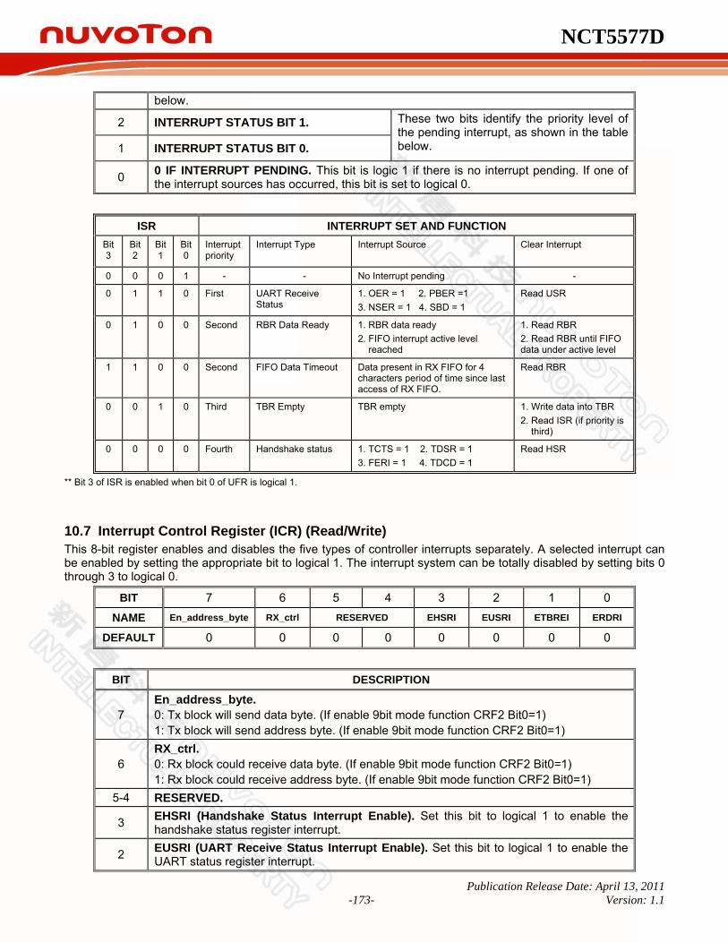
NCT5577D
Publication Release Date: April 13, 2011 -173- Version: 1.1
below.
2 INTERRUPT STATUS BIT 1.
1 INTERRUPT STATUS BIT 0.
These two bits identify the priority level of the pending interrupt, as shown in the table below.
0 0 IF INTERRUPT PENDING. This bit is logic 1 if there is no interrupt pending. If one of the interrupt sources has occurred, this bit is set to logical 0.
ISR INTERRUPT SET AND FUNCTION Bit 3
Bit 2
Bit 1
Bit 0
Interrupt priority
Interrupt Type
Interrupt Source
Clear Interrupt
0 0 0 1 - - No Interrupt pending -
0 1 1 0 First UART Receive Status
1. OER = 1 2. PBER =1 3. NSER = 1 4. SBD = 1
Read USR
0 1 0 0 Second RBR Data Ready 1. RBR data ready 2. FIFO interrupt active level reached
1. Read RBR 2. Read RBR until FIFO data under active level
1 1 0 0 Second FIFO Data Timeout Data present in RX FIFO for 4 characters period of time since last access of RX FIFO.
Read RBR
0 0 1 0 Third TBR Empty TBR empty 1. Write data into TBR 2. Read ISR (if priority is third)
0 0 0 0 Fourth Handshake status 1. TCTS = 1 2. TDSR = 1 3. FERI = 1 4. TDCD = 1
Read HSR
** Bit 3 of ISR is enabled when bit 0 of UFR is logical 1.
10.7 Interrupt Control Register (ICR) (Read/Write) This 8-bit register enables and disables the five types of controller interrupts separately. A selected interrupt can be enabled by setting the appropriate bit to logical 1. The interrupt system can be totally disabled by setting bits 0 through 3 to logical 0.
BIT 7 6 5 4 3 2 1 0 NAME En_address_byte RX_ctrl RESERVED EHSRI EUSRI ETBREI ERDRI
DEFAULT 0 0 0 0 0 0 0 0
BIT DESCRIPTION
7 En_address_byte. 0: Tx block will send data byte. (If enable 9bit mode function CRF2 Bit0=1) 1: Tx block will send address byte. (If enable 9bit mode function CRF2 Bit0=1)
6 RX_ctrl. 0: Rx block could receive data byte. (If enable 9bit mode function CRF2 Bit0=1) 1: Rx block could receive address byte. (If enable 9bit mode function CRF2 Bit0=1)
5-4 RESERVED.
3 EHSRI (Handshake Status Interrupt Enable). Set this bit to logical 1 to enable the handshake status register interrupt.
2 EUSRI (UART Receive Status Interrupt Enable). Set this bit to logical 1 to enable the UART status register interrupt.

NCT5577D
Publication Release Date: April 13, 2011 -174- Version: 1.1
BIT DESCRIPTION
1 ETBREI (TBR Empty Interrupt Enable). Set this bit to logical 1 to enable the TBR empty interrupt.
0 ERDRI (RBR Data Ready Interrupt Enable). Set this bit to logical 1 to enable the RBR data ready interrupt.
10.8 Programmable Baud Generator (BLL/BHL) (Read/Write) Two 8-bit registers, BLL and BHL, compose a programmable baud generator that uses 24 MHz to generate a 1.8461 MHz frequency and divide it by a divisor from 1 to (216 –1). The output frequency of the baud generator is the baud rate multiplied by 16, and this is the base frequency for the transmitter and receiver. The table below illustrates the use of the baud generator with a frequency of 1.8461 MHz. In high-speed UART mode (CR0C, bits 7 and 6), the programmable baud generator directly uses 24 MHz and the same divisor as the normal speed divisor. As a result, in high-speed mode, the data transmission rate can be as high as 1.5M bps.
BAUD RATE FROM DIFFERENT PRE-DIVIDER PRE-DIV: 13 1.8461M HZ
PRE-DIV:1.625
14.769M HZ
PRE-DIV: 1.0
24M HZ
DECIMAL DIVISOR USED TO
GENERATE 16X CLOCK
ERROR PERCENTAGE
50 400 650 2304 ** 75 600 975 1536 **
110 880 1430 1047 0.18% 134.5 1076 1478.5 857 0.099% 150 1200 1950 768 ** 300 2400 3900 384 ** 600 4800 7800 192 ** 1200 9600 15600 96 ** 1800 14400 23400 64 ** 2000 16000 26000 58 0.53% 2400 19200 31200 48 ** 3600 28800 46800 32 ** 4800 38400 62400 24 ** 7200 57600 93600 16 ** 9600 76800 124800 12 ** 19200 153600 249600 6 ** 38400 307200 499200 3 ** 57600 460800 748800 2 **
115200 921600 1497600 1 ** ** Unless specified, the error percentage for all of the baud rates is 0.16%.
Note: Pre-Divisor is determined by CRF0 of UART A.
10.9 User-defined Register (UDR) (Read/Write) This is a temporary register that can be accessed and defined by the user.

NCT5577D
Publication Release Date: April 13, 2011 -175- Version: 1.1
10.10 UART RS485 Auto Flow Control NCT5577D supports RS485 auto flow control function for UARTA. When enabling the RS485 auto control function, it will automatically drive RTS# pin to logic high or low for UARTA when UART TX block transmits the data. The diagram shown below illustrates the RS485 auto flow control function for UARTA.
The default behavior of RTS# pin will drive logic high the time edge between Start bit and bit0 when the UART TX Block start to transmits the data on SOUT pin. Then the RTS# pin will drive logic low later than Stop bit about 1~2 x Bit-time when UART TX Block completes the data transmission. The driving behavior of RTS# will be inverted when we set RS485_RTS_inv_sel bit = 1’b1. (Bit-time: Depends on the baud rate of transmission) The bellowing control register table relates to the RS485 auto flow control function for UARTA.
UARTA
RTS485_enable Logic Device 2, CRF2_Bit7
RTS485_inv_sel Logic Device 2, CRF2_Bit6

NCT5577D
Publication Release Date: April 13, 2011 -176- Version: 1.1
11. KEYBOARD CONTROLLER The NCT5577D KBC (8042 with licensed KB BIOS) circuit is designed to provide the functions needed to interface a CPU with a keyboard and/or a PS/2 mouse and can be used with IBM®-compatible personal computers or PS/2-based systems. The controller receives serial data from the keyboard or PS/2 mouse, checks the parity of the data, and presents the data to the system as a byte of data in its output buffer. Then, the controller asserts an interrupt to the system when data are placed in its output buffer. The keyboard and PS/2 mouse are required to acknowledge all data transmissions. No transmission should be sent to the keyboard or PS/2 mouse until an acknowledgement is received for the previous data byte.
8042
P24P25
P21P20
P27
P10P26
T0
P23
T1
P22
P11
KIRQMIRQGATEA20
KBRSTP17KINH
GP I/O PINSP12~P16
KDAT
KCLK
MCLK
MDAT
Multiplex I/O PINS
Figure 11-1 Keyboard and Mouse Interface
11.1 Output Buffer The output buffer is an 8-bit, read-only register at I/O address 60H (Default, PnP programmable I/O address LD5-CR60 and LD5-CR61). The keyboard controller uses the output buffer to send the scan code (from the keyboard) and required command bytes to the system. The output buffer can only be read when the output buffer full bit in the register (in the status register) is logical 1.
11.2 Input Buffer The input buffer is an 8-bit, write-only register at I/O address 60h or 64h (Default, PnP programmable I/O address LD5-CR60, LD5-CR61, LD5-CR62, and LD5-CR63). Writing to address 60h sets a flag to indicate a data write; writing to address 64h sets a flag to indicate a command write. Data written to I/O address 60h is sent to the keyboard (unless the keyboard controller is expecting a data byte) through the controller’s input buffer only if the input buffer full bit (in the status register) is logical 0.

NCT5577D
Publication Release Date: April 13, 2011 -177- Version: 1.1
11.3 Status Register The status register is an 8-bit, read-only register at I/O address 64h (Default, PnP programmable I/O address LD5-CR62 and LD5-CR63) that holds information about the status of the keyboard controller and interface. It may be read at any time.
Table 11-1 Bit Map of Status Register
BIT BUT FUNCTION DESCRIPTION 0 Output Buffer Full 0: Output buffer empty
1: Output buffer full 1 Input Buffer Full 0: Input buffer empty
1: Input buffer full 2 System Flag This bit may be set to 0 or 1 by writing to the system flag
bit in the command byte of the keyboard controller. It defaults to 0 after a power-on reset.
3 Command/Data 0: Data byte 1: Command byte
4 Inhibit Switch 0: Keyboard is inhibited 1: Keyboard is not inhibited
5 Auxiliary Device Output Buffer
0: Auxiliary device output buffer empty 1: Auxiliary device output buffer full
6 General Purpose Time-out
0: No time-out error 1: Time-out error
7 Parity Error 0: Odd parity 1: Even parity (error)
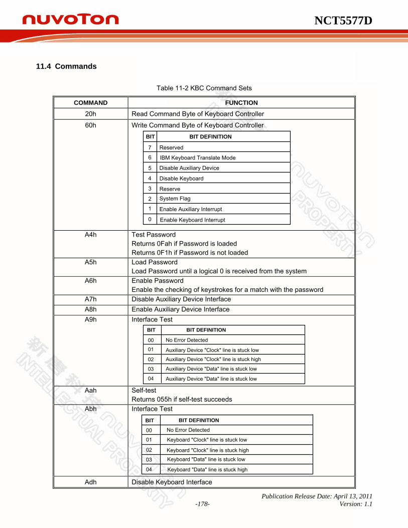
NCT5577D
Publication Release Date: April 13, 2011 -178- Version: 1.1
11.4 Commands
Table 11-2 KBC Command Sets
COMMAND FUNCTION
20h Read Command Byte of Keyboard Controller
60h Write Command Byte of Keyboard Controller
BIT
1
2
3
4
5
6
7
0
BIT DEFINITION
Reserved
IBM Keyboard Translate Mode
Disable Auxiliary Device
Disable Keyboard
Reserve
System Flag
Enable Auxiliary Interrupt
Enable Keyboard Interrupt
A4h Test Password Returns 0Fah if Password is loaded Returns 0F1h if Password is not loaded
A5h Load Password Load Password until a logical 0 is received from the system
A6h Enable Password Enable the checking of keystrokes for a match with the password
A7h Disable Auxiliary Device Interface A8h Enable Auxiliary Device Interface A9h Interface Test
BIT
04
03
02
01
00
BIT DEFINITION
No Error Detected
Auxiliary Device "Clock" line is stuck low
Auxiliary Device "Clock" line is stuck high
Auxiliary Device "Data" line is stuck low
Auxiliary Device "Data" line is stuck low Aah Self-test
Returns 055h if self-test succeeds Abh Interface Test
BIT
04
03
02
01
00
BIT DEFINITION
No Error Detected
Keyboard "Clock" line is stuck low
Keyboard "Clock" line is stuck high
Keyboard "Data" line is stuck low
Keyboard "Data" line is stuck high Adh Disable Keyboard Interface
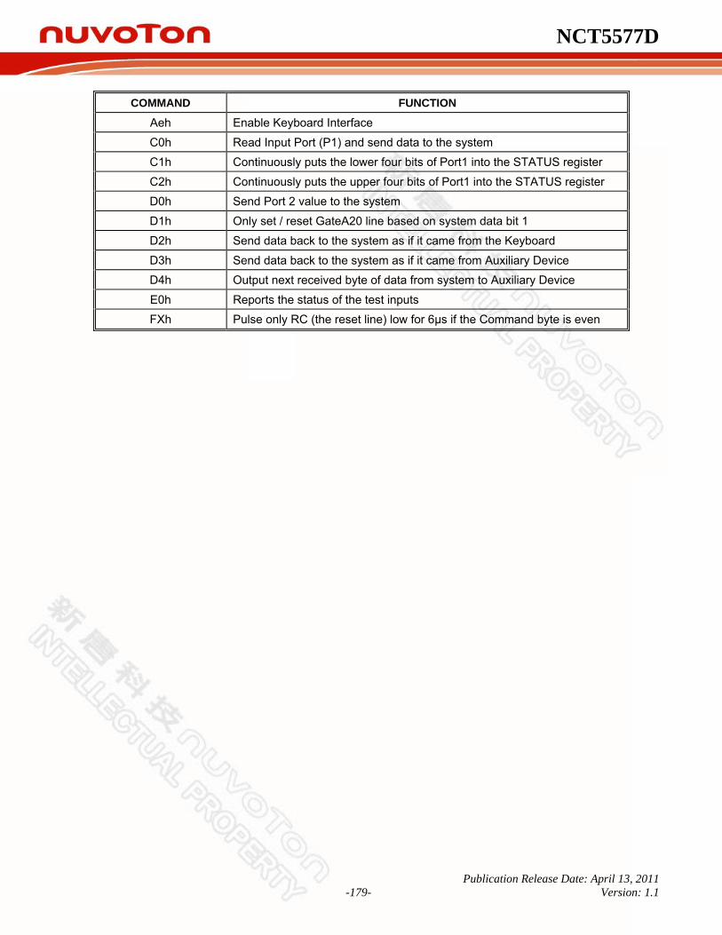
NCT5577D
Publication Release Date: April 13, 2011 -179- Version: 1.1
COMMAND FUNCTION
Aeh Enable Keyboard Interface
C0h Read Input Port (P1) and send data to the system C1h Continuously puts the lower four bits of Port1 into the STATUS register
C2h Continuously puts the upper four bits of Port1 into the STATUS register D0h Send Port 2 value to the system
D1h Only set / reset GateA20 line based on system data bit 1 D2h Send data back to the system as if it came from the Keyboard
D3h Send data back to the system as if it came from Auxiliary Device D4h Output next received byte of data from system to Auxiliary Device
E0h Reports the status of the test inputs FXh Pulse only RC (the reset line) low for 6μs if the Command byte is even

NCT5577D
Publication Release Date: April 13, 2011 -180- Version: 1.1
11.5 Hardware GATEA20/Keyboard Reset Control Logic The KBC includes hardware control logic to speed-up GATEA20 and KBRESET. This control logic is controlled by LD5-CRF0 as follows:
11.5.1 KB Control Register (Logic Device 5, CR-F0) BIT 7 6 5 4 3 2 1 0
NAME KCLKS1 KCLKS0 RESERVED P92EN HGA20 HKBRST#
DEFAULT 1 0 0 0 0 0 0 0
BIT DESCRIPTION
7 KCLKS1.
6 KCLKS0.
Select the KBC clock rate. Bits 7 6 0 0: Reserved 0 1: Reserved 1 0: KBC clock input is 12 MHz. 1 1: Reserved
5-3 RESERVED.
2 P92EN (Port 92 Enable). 1: Enables Port 92 to control GATEA20 and KBRESET. 0: Disables Port 92 functions.
1 HGA20 (Hardware GATEA 20). 1: Selects hardware GATE A20 control logic to control GATE A20 signal. 0: Disables GATEA20 control logic functions.
0 HKBRST# (Hardware Keyboard Reset). 1: Selects hardware KB RESET control logic to control KBRESET signal. 0: Disables hardware KB RESET control logic function.
When the KBC receives data that follows a “D1” command, the hardware control logic sets or clears GATE A20 according to received data bit 1. Similarly, the hardware control logic sets or clears KBRESET depending on received data bit 0. When the KBC receives an “FE” command, the KBRESET is pulse low for 6 μs (Min.) with a 14 μs (Min.) delay. GATE A20 and KBRESET are controlled by either software or hardware logic, and they are mutually exclusive. Then, GATE A20 and KBRESET are merged with Port92 when the P92EN bit is set.

NCT5577D
Publication Release Date: April 13, 2011 -181- Version: 1.1
11.5.2 Port 92 Control Register (Default Value = 0x24)
BIT 7 6 5 4 3 2 1 0 NAME RES. (0) RES. (1) RES. (0) RES. (1) SGA20 PLKBRST#
DEFAULT 0 0 1 0 0 1 0 0
BIT DESCRIPTION
7-6 RES. (0) 5 RES. (1)
4-3 RES. (0) 2 RES. (1)
1 SGA20 (Special GATE A20 Control) 1: Drives GATE A20 signal to high. 0: Drives GATE A20 signal to low.
0 PLKBRST# (Pulled-low KBRESET). A logical 1 on this bit causes KBRESET to drive low for 6 μS(Min.) with a 14 μS(Min.) delay. Before issuing another keyboard-reset command, the bit must be cleared.
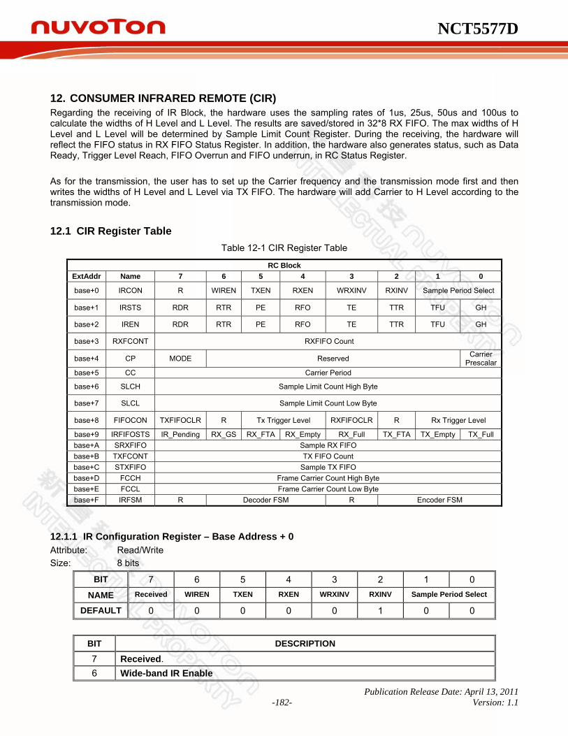
NCT5577D
Publication Release Date: April 13, 2011 -182- Version: 1.1
12. CONSUMER INFRARED REMOTE (CIR) Regarding the receiving of IR Block, the hardware uses the sampling rates of 1us, 25us, 50us and 100us to calculate the widths of H Level and L Level. The results are saved/stored in 32*8 RX FIFO. The max widths of H Level and L Level will be determined by Sample Limit Count Register. During the receiving, the hardware will reflect the FIFO status in RX FIFO Status Register. In addition, the hardware also generates status, such as Data Ready, Trigger Level Reach, FIFO Overrun and FIFO underrun, in RC Status Register. As for the transmission, the user has to set up the Carrier frequency and the transmission mode first and then writes the widths of H Level and L Level via TX FIFO. The hardware will add Carrier to H Level according to the transmission mode.
12.1 CIR Register Table Table 12-1 CIR Register Table
RC Block ExtAddr Name 7 6 5 4 3 2 1 0
base+0 IRCON R WIREN TXEN RXEN WRXINV RXINV Sample Period Select
base+1 IRSTS RDR RTR PE RFO TE TTR TFU GH
base+2 IREN RDR RTR PE RFO TE TTR TFU GH
base+3 RXFCONT RXFIFO Count
base+4 CP MODE Reserved Carrier Prescalar
base+5 CC Carrier Period
base+6 SLCH Sample Limit Count High Byte
base+7 SLCL Sample Limit Count Low Byte
base+8 FIFOCON TXFIFOCLR R Tx Trigger Level RXFIFOCLR R Rx Trigger Level
base+9 IRFIFOSTS IR_Pending RX_GS RX_FTA RX_Empty RX_Full TX_FTA TX_Empty TX_Fullbase+A SRXFIFO Sample RX FIFO base+B TXFCONT TX FIFO Count base+C STXFIFO Sample TX FIFO base+D FCCH Frame Carrier Count High Byte base+E FCCL Frame Carrier Count Low Byte base+F IRFSM R Decoder FSM R Encoder FSM
12.1.1 IR Configuration Register – Base Address + 0 Attribute: Read/Write Size: 8 bits
BIT 7 6 5 4 3 2 1 0
NAME Received WIREN TXEN RXEN WRXINV RXINV Sample Period Select
DEFAULT 0 0 0 0 0 1 0 0
BIT DESCRIPTION
7 Received. 6 Wide-band IR Enable
NCT5577D
Publication Release Date: April 13, 2011 -183- Version: 1.1
5 TX Enable 1: Transmission Enable. After confirming that FIFO is not empty, the transmission starts
(the hardware will wait until TX FIFO data are written). If TX Enable is set to 0 during the transmission, the transmission stops when the transmission of FIFO data is completed.
0: Transmission Disable. 4 RX Enable 3 Wide-band IR Rx Invert Enable
0: Dongle Carrier ON is high, OFF (Idle) is low. 1: Dongle Carrier ON is low, OFF (Idle) is high.
2 IR Rx Invert Enable 0: Dongle Carrier ON is high, OFF (Idle) is low. 1: Dongle Carrier ON is low, OFF (Idle) is high.
1~0 Sample Period Select 00:1us, 01: 25us, 10: 50us, 11: 100us Note: In the 1us mode, the pulse mode will not function due to the IR regulations.
12.1.2 IR Status Register – Base Address + 1 Attribute: Read/Write Size: 8 bits
BIT 7 6 5 4 3 2 1 0 Name RDR RTR PE RFO TE TTR TFU GH
DEFAULT 0 0 0 0 0 0 0 0
BIT DESCRIPTION
7 RX Data Ready (Writing 1 will clear the bit). 6 RX FIFO Trigger Level Reach (Writing 1 will clear the bit). 5 Packet End (Writing 1 will clear the bit). 4 RX FIFO Overrun (Overrun and Data Ready will be simultaneously generated. Writing 1
will clear the bit). 3 TX FIFO Empty (Writing 1 will clear the bit). 2 TX FIFO Trigger Level Reach (Writing 1 will clear the bit). 1 TX FIFO Underrun (Writing 1 will clear the bit). 0 Min Length Detected (Writing 1 will clear the bit)
1: The IR Data length received is shorter than the default value. 0: The IR Data length received is longer than the default value.
12.1.3 IR Interrupt Configuration Register – Base Address + 2 Attribute: Read/Write Size: 8 bits
BIT 7 6 5 4 3 2 1 0

NCT5577D
Publication Release Date: April 13, 2011 -184- Version: 1.1
NAME RDR RTR PE RFO TE TTR TFU GH
DEFAULT 0 0 0 0 0 0 0 0
1: Enable interrupt; 0: Disable interrupt
BIT DESCRIPTION
7 RX Data Ready
6 RX FIFO Trigger Level Reach
5 Packet End 4 RX FIFO Overrun (Overrun and Data Ready will be simultaneously generated).
3 TX FIFO Empty 2 TX FIFO Trigger Level Reach 1 TX FIFO Underrun 0 Min Length Detected
Note. When an Interrupt occurs, it only can be cleared by writing IR Status Register to 1.
12.1.4 RX FIFO Count– Base Address + 5 Attribute: Read Size: 8 bits
BIT 7 6 5 4 3 2 1 0
NAME FIFO Count
DEFAULT 0 0 0 0 0 0 0 0
1: Enable; 0: Disable
BIT DESCRIPTION
7~0 RX FIFO Count
12.1.5 IR TX Carrier Prescalar Configuration Register (CP) – Base Address + 4 Attribute: Read/Write Size: 8 bits
BIT 7 6 5 4 3 2 1 0
NAME Mode Reserved CP
DEFAULT 0 0 0 0 0 0 0 0
BIT DESCRIPTION
7 Mode 0 : DC Mode 1 : Pulse Mode
6~1 Reserved. 0 Carrier Prescalar (CP). This bit is set for the Prescalar value of the IR TX carrier
NCT5577D
Publication Release Date: April 13, 2011 -185- Version: 1.1
frequency.
12.1.6 IR TX Carrier Period Configuration Register (CC) – Base Address + 5 Attribute: Read/Write Size: 8 bits
BIT 7 6 5 4 3 2 1 0
NAME Carrier Period (CC)
DEFAULT 0 0 0 0 0 0 0 0
BIT DESCRIPTION
7~0 This byte is set for IR TX carrier period. The actual carrier period will be: Period = 2 * (2 ^ (CP*2)) * (CC+1) / (System Clock), where the frequency = 1 / period, and System Clock = 24MHz. Setting CP and CC to 0 will cause stop the device to from use using anyno carrier at all (that is, no light modulation, just constant on and off periods). The period count value CC can be any number from 0 to 255.
12.1.7 IR RX Sample Limited Count High Byte Register (RCLCH) – Base Address + 6 Attribute: Read/Write Size: 8 bits
BIT 7 6 5 4 3 2 1 0 NAME Sample Limited Count High Byte
DEFAULT 0 0 0 0 0 0 0 0
BIT DESCRIPTION
7~0 This byte is defined as the high byte of the limited count in the IR RX mode.
12.1.8 IR RX Sample Limited Count Low Byte Register (RCLCL) – Base Address + 7 Attribute: Read/Write Size: 8 bits
BIT 7 6 5 4 3 2 1 0
NAME Sample Limited Count low Byte
DEFAULT 0 0 0 0 0 0 0 0
BIT DESCRIPTION
7~0 This byte is defined as the low byte of the limited count in the IR RX mode.
Note. (RCLCH, RCLCL) is defined as 16 bits value of the limited count in the IR RX mode. When the RX date length reaches the limited count, Packet End status will appear.
12.1.9 IR FIFO Configuration Register (FIFOCON) – Base Address + 8 Attribute: Read/Write
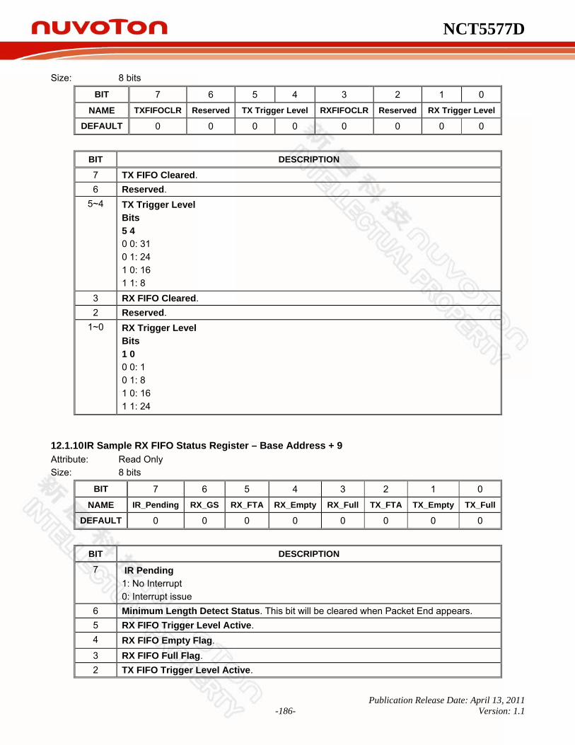
NCT5577D
Publication Release Date: April 13, 2011 -186- Version: 1.1
Size: 8 bits
BIT 7 6 5 4 3 2 1 0
NAME TXFIFOCLR Reserved TX Trigger Level RXFIFOCLR Reserved RX Trigger Level
DEFAULT 0 0 0 0 0 0 0 0
BIT DESCRIPTION
7 TX FIFO Cleared. 6 Reserved.
5~4 TX Trigger Level Bits 5 4 0 0: 31 0 1: 24 1 0: 16 1 1: 8
3 RX FIFO Cleared. 2 Reserved.
1~0 RX Trigger Level Bits 1 0 0 0: 1 0 1: 8 1 0: 16 1 1: 24
12.1.10 IR Sample RX FIFO Status Register – Base Address + 9 Attribute: Read Only Size: 8 bits
BIT 7 6 5 4 3 2 1 0
NAME IR_Pending RX_GS RX_FTA RX_Empty RX_Full TX_FTA TX_Empty TX_Full
DEFAULT 0 0 0 0 0 0 0 0
BIT DESCRIPTION
7 IR Pending 1: No Interrupt 0: Interrupt issue
6 Minimum Length Detect Status. This bit will be cleared when Packet End appears. 5 RX FIFO Trigger Level Active. 4 RX FIFO Empty Flag. 3 RX FIFO Full Flag. 2 TX FIFO Trigger Level Active.
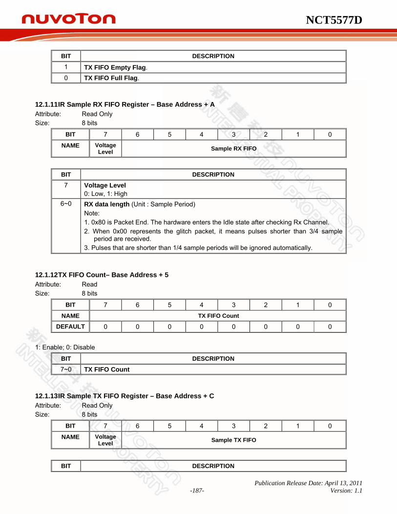
NCT5577D
Publication Release Date: April 13, 2011 -187- Version: 1.1
BIT DESCRIPTION
1 TX FIFO Empty Flag. 0 TX FIFO Full Flag.
12.1.11 IR Sample RX FIFO Register – Base Address + A Attribute: Read Only Size: 8 bits
BIT 7 6 5 4 3 2 1 0
NAME Voltage Level Sample RX FIFO
BIT DESCRIPTION
7 Voltage Level 0: Low, 1: High
6~0 RX data length (Unit : Sample Period) Note: 1. 0x80 is Packet End. The hardware enters the Idle state after checking Rx Channel. 2. When 0x00 represents the glitch packet, it means pulses shorter than 3/4 sample
period are received. 3. Pulses that are shorter than 1/4 sample periods will be ignored automatically.
12.1.12 TX FIFO Count– Base Address + 5 Attribute: Read Size: 8 bits
BIT 7 6 5 4 3 2 1 0 NAME TX FIFO Count
DEFAULT 0 0 0 0 0 0 0 0
1: Enable; 0: Disable
BIT DESCRIPTION
7~0 TX FIFO Count
12.1.13 IR Sample TX FIFO Register – Base Address + C Attribute: Read Only Size: 8 bits
BIT 7 6 5 4 3 2 1 0
NAME Voltage Level Sample TX FIFO
BIT DESCRIPTION
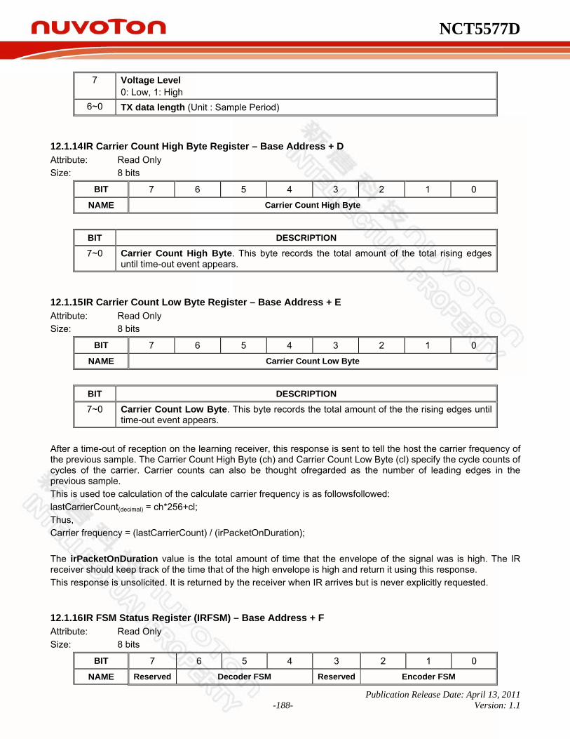
NCT5577D
Publication Release Date: April 13, 2011 -188- Version: 1.1
7 Voltage Level 0: Low, 1: High
6~0 TX data length (Unit : Sample Period)
12.1.14 IR Carrier Count High Byte Register – Base Address + D Attribute: Read Only Size: 8 bits
BIT 7 6 5 4 3 2 1 0
NAME Carrier Count High Byte
BIT DESCRIPTION
7~0 Carrier Count High Byte. This byte records the total amount of the total rising edges until time-out event appears.
12.1.15 IR Carrier Count Low Byte Register – Base Address + E Attribute: Read Only Size: 8 bits
BIT 7 6 5 4 3 2 1 0
NAME Carrier Count Low Byte
BIT DESCRIPTION
7~0 Carrier Count Low Byte. This byte records the total amount of the the rising edges until time-out event appears.
After a time-out of reception on the learning receiver, this response is sent to tell the host the carrier frequency of the previous sample. The Carrier Count High Byte (ch) and Carrier Count Low Byte (cl) specify the cycle counts of cycles of the carrier. Carrier counts can also be thought ofregarded as the number of leading edges in the previous sample. This is used toe calculation of the calculate carrier frequency is as followsfollowed: lastCarrierCount(decimal) = ch*256+cl; Thus, Carrier frequency = (lastCarrierCount) / (irPacketOnDuration); The irPacketOnDuration value is the total amount of time that the envelope of the signal was is high. The IR receiver should keep track of the time that of the high envelope is high and return it using this response. This response is unsolicited. It is returned by the receiver when IR arrives but is never explicitly requested.
12.1.16 IR FSM Status Register (IRFSM) – Base Address + F Attribute: Read Only Size: 8 bits
BIT 7 6 5 4 3 2 1 0 NAME Reserved Decoder FSM Reserved Encoder FSM

NCT5577D
Publication Release Date: April 13, 2011 -189- Version: 1.1
DEFAULT 0 0 0 0 0 0 0 0
BIT DESCRIPTION
7 Reserved. 6 Decoder over status 5 Decoder continuing status 4 Decoder wait H status
1: idle, 0: RX busy 3 Reserved. 2 Encoder Idle Status.
1: idle, 0: TX busy 1 Encoder Read Status 0 Encoder Level Output Status
12.1.17 IR Minimum Length Register – Base Address + F Attribute: Write Only Size: 8 bits
BIT 7 6 5 4 3 2 1 0
NAME Min Length Register
DEFAULT 0 0 0 0 0 0 0 0
BIT DESCRIPTION
7~0 Min Length Register. Set up the shortest expected length of each carrier on the RX receiver (Unit: Sample Clock).

NCT5577D
Publication Release Date: April 13, 2011 -190- Version: 1.1
13. CONSUMER INFRARED REMOTE (CIR) WAKE-UP One of the features of the NCT5577D is system boot-up by a remote controller. The hardware will store a specifically appointed key command from the IR remote controller in the FIFO of 67Byte. The same key is required to re-boot the system after the computer shut-down. Such way can be applied to any remote controllers. Learning is necessary only at the first time.
13.1 CIR WAKE-UP Register Table RC Block
ExtAddr Name 7 6 5 4 3 2 1 0
base+0 IRCON DEC_RST Mode[1] Mode[0] RXEN IgnoreEN RXINV Sample Period Select
base+1 IRSTS RDR RTR PE RFO GH R R IR Pending
base+2 IREN RDR RTR PE RFO GH R
Base+3 FIFO_COMPARE_DEEP
base+4 FIFO_COMPARE_TOLERANCE base+5 FIFO_Count
Base+6 SLCH Sample Limit Count High Byte
base+7 SLCL Sample Limit Count Low Byte
base+8 FIFOCON R RXFIFOCLR R Rx Trigger Level
base+9 SRXFSTS GS FTA Empty Full R base+A Sample RX FIFO base+B WR_FIFO_DATA Base+C Read FIFO Only Base+D Read FIFO Only Index Base+E FIFO_Ignore
Base+F IRFSM R Decoder FSM R Wakeup Event
13.1.1 IR Configuration Register – Base Address + 0 Attribute: Read/Write Size: 8 bits
BIT 7 6 5 4 3 2 1 0 NAME DEC_RST Mode[1] Mode[0] RXEN Received RXINV Sample Period Select
DEFAULT 0 0 1 0 0 1 1 0
BIT DESCRIPTION 7 Reset CIR DECODER ( Write 1 to clear) 6 Mode[1] :
0: FIFO can’t be written 1: FIFO can be written
5 Mode[0] 0: Learning Mode

NCT5577D
Publication Release Date: April 13, 2011 -191- Version: 1.1
BIT DESCRIPTION 1: Wake up Mode (Before enter in Power S3 state, this bit should be set) This bit reset by VCC.
4 RX Enable 3 Ignore Bit Enable 2 IR Rx Invert Enable
0: Dongle Carrier ON is high, OFF (Idle) is low. 1: Dongle Carrier ON is low, OFF (Idle) is high.
1~0 Sample Period Select 00:1us, 01: 25us, 10: 50us, 11: 100us Note: In the 1us mode, the pulse mode will not function due to the IR regulations.
13.1.2 IR Status Register – Base Address + 1 Attribute: Read/Write Size: 8 bits
BIT 7 6 5 4 3 2 1 0
NAME RDR RTR PE RFO GH Received IR_Pending
DEFAULT 0 0 0 0 0 0 0 0
BIT DESCRIPTION
7 RX Data Ready (Writing 1 will clear the bit). 6 RX FIFO Trigger Level Reach (Writing 1 will clear the bit). 5 Packet End (Writing 1 will clear the bit). 4 RX FIFO Overrun (Overrun and Data Ready will be simultaneously generated. Writing 1
will clear the bit). 3 Min Length Detected (Writing 1 will clear the bit)
1: The IR Data length received is shorter than the default value. 0: The IR Data length received is longer than the default value.
2~1 Reserved. 0 IR Pending
1: No Interrupt 0: Interrupt issue
13.1.3 IR Interrupt Configuration Register – Base Address + 2 Attribute: Read/Write Size: 8 bits
BIT 7 6 5 4 3 2 1 0
NAME RDR RTR PE RFO GH Reserved
DEFAULT 0 0 0 0 0 0 0 0
1: Enable interrupt; 0: Disable interrupt
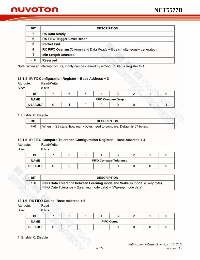
NCT5577D
Publication Release Date: April 13, 2011 -192- Version: 1.1
BIT DESCRIPTION
7 RX Data Ready 6 RX FIFO Trigger Level Reach 5 Packet End 4 RX FIFO Overrun (Overrun and Data Ready will be simultaneously generated). 3 Min Length Detected
2~0 Reserved
Note. When an Interrupt occurs, it only can be cleared by writing IR Status Register to 1.
13.1.4 IR TX Configuration Register – Base Address + 3 Attribute: Read/Write Size: 8 bits
BIT 7 6 5 4 3 2 1 0
NAME FIFO Compare Deep
DEFAULT 0 1 0 0 0 0 1 1
1: Enable; 0: Disable
BIT DESCRIPTION
7~0 When in S3 state, how many bytes need to compare. Default is 67 bytes.
13.1.5 IR FIFO Compare Tolerance Configuration Register – Base Address + 4 Attribute: Read/Write Size: 8 bits
BIT 7 6 5 4 3 2 1 0 NAME FIFO Compare Tolerance
DEFAULT 0 0 0 0 0 0 0 0
BIT DESCRIPTION
7~0 FIFO Data Tolerance between Learning mode and Wakeup mode. (Every byte) FIFO Date Tolerance = (Learning mode data) – (Wakeup mode data)
13.1.6 RX FIFO Count– Base Address + 5 Attribute: Read Size: 8 bits
BIT 7 6 5 4 3 2 1 0
NAME FIFO Count
DEFAULT 0 0 0 0 0 0 0 0
1: Enable; 0: Disable
NCT5577D
Publication Release Date: April 13, 2011 -193- Version: 1.1
BIT DESCRIPTION
7~0 RX FIFO Count
13.1.7 IR RX Sample Limited Count High Byte Register (RCLCH) – Base Address + 6 Attribute: Read/Write Size: 8 bits
BIT 7 6 5 4 3 2 1 0
NAME Sample Limited Count High Byte
DEFAULT 0 0 0 0 0 0 0 0
BIT DESCRIPTION
7~0 This byte is defined as the high byte of the limited count in the IR RX mode.
13.1.8 IR RX Sample Limited Count Low Byte Register (RCLCL) – Base Address + 7 Attribute: Read/Write Size: 8 bits
BIT 7 6 5 4 3 2 1 0
NAME Sample Limited Count low Byte
DEFAULT 0 0 0 0 0 0 0 0
BIT DESCRIPTION
7~0 This byte is defined as the low byte of the limited count in the IR RX mode.
Note. (RCLCH, RCLCL) is defined as 16 bits value of the limited count in the IR RX mode. When the RX date length reaches the limited count, Packet End status will appear.
13.1.9 IR FIFO Configuration Register (FIFOCON) – Base Address + 8 Attribute: Read/Write Size: 8 bits
BIT 7 6 5 4 3 2 1 0
NAME Reserved RXFIFOCLR Reserved RX Trigger Level
DEFAULT 0 0 0 0 0 0 0 0
BIT DESCRIPTION
7~4 Reserved 3 RX FIFO Cleared. 2 Reserved.
1~0 RX Trigger Level Bits 1 0 0 0: 67
NCT5577D
Publication Release Date: April 13, 2011 -194- Version: 1.1
0 1: 66 1 0: 65 1 1: 64
13.1.10 IR Sample RX FIFO Status Register – Base Address + 9 Attribute: Read Only Size: 8 bits
BIT 7 6 5 4 3 2 1 0
NAME GS FTA Empty Full Reserved
DEFAULT 0 0 0 0 0 0 0 0
BIT DESCRIPTION
7 Minimum Length Detect Status. This bit will be cleared when Packet End appears. 6 RX FIFO Trigger Level Active. 5 RX FIFO Empty Flag. 4 RX FIFO Full Flag.
3~0 Reserved
13.1.11 IR Sample RX FIFO Register – Base Address + A Attribute: Read Only Size: 8 bits
BIT 7 6 5 4 3 2 1 0 NAME Voltage
Level Sample RX FIFO
BIT DESCRIPTION
7~6 Voltage Level 0: Low, 1: High
0 RX data length (Unit : Sample Period) Note: 1. 0x80 is Packet End. The hardware enters the Idle state after checking Rx Channel. 2. When 0x00 represents the glitch packet, it means pulses shorter than 3/4 sample
period are received. 3. Pulses that are shorter than 1/4 sample periods will be ignored automatically.
13.1.12 Write FIFO – Base Address + B Attribute: Write Only Size: 8 bits
BIT 7 6 5 4 3 2 1 0
NAME Voltage Level Write Sample RX FIFO

NCT5577D
Publication Release Date: April 13, 2011 -195- Version: 1.1
BIT DESCRIPTION
7~6 Voltage Level 0: Low, 1: High
0 RX data length (Unit : Sample Period)
Note. Before writing FIFO Data, mode[1] register should be set.
13.1.13 Read FIFO Only – Base Address + C Attribute: Read Only Size: 8 bits
BIT 7 6 5 4 3 2 1 0
NAME Voltage Level Sample RX FIFO
BIT DESCRIPTION
7~6 Voltage Level 0: Low, 1: High
0 RX data length (Unit : Sample Period)
Note. Only Read FIFO Data.
13.1.14 Read FIFO Index – Base Address + D Attribute: Read Only Size: 8 bits
BIT 7 6 5 4 3 2 1 0
NAME FIFO Index
BIT DESCRIPTION
7~0 Indicate that FIFO Index when only read FIFO data(Base Address + C)
Note. Only Read FIFO Data.
13.1.15 Reserved – Base Address + E
13.1.16 IR FSM Status Register (IRFSM) – Base Address + F Attribute: Read Only Size: 8 bits
BIT 7 6 5 4 3 2 1 0
NAME Reserved Decoder FSM Reserved Wakeup event
DEFAULT 0 0 0 0 0 0 0 0
13.1.17 IR Minimum Length Register – Base Address + F

NCT5577D
Publication Release Date: April 13, 2011 -196- Version: 1.1
Attribute: Write Only Size: 8 bits
BIT 7 6 5 4 3 2 1 0
NAME Min Length Register
DEFAULT 0 0 0 0 0 0 0 0
BIT DESCRIPTION
7~0 Min Length Register. Set up the shortest expected length of each carrier on the RX receiver (Unit: Sample Clock).
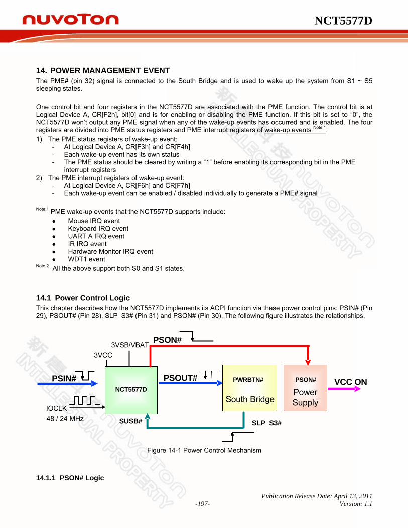
NCT5577D
Publication Release Date: April 13, 2011 -197- Version: 1.1
14. POWER MANAGEMENT EVENT The PME# (pin 32) signal is connected to the South Bridge and is used to wake up the system from S1 ~ S5 sleeping states. One control bit and four registers in the NCT5577D are associated with the PME function. The control bit is at Logical Device A, CR[F2h], bit[0] and is for enabling or disabling the PME function. If this bit is set to “0”, the NCT5577D won’t output any PME signal when any of the wake-up events has occurred and is enabled. The four registers are divided into PME status registers and PME interrupt registers of wake-up events Note.1. 1) The PME status registers of wake-up event:
- At Logical Device A, CR[F3h] and CR[F4h] - Each wake-up event has its own status - The PME status should be cleared by writing a “1” before enabling its corresponding bit in the PME
interrupt registers 2) The PME interrupt registers of wake-up event:
- At Logical Device A, CR[F6h] and CR[F7h] - Each wake-up event can be enabled / disabled individually to generate a PME# signal
Note.1 PME wake-up events that the NCT5577D supports include: Mouse IRQ event Keyboard IRQ event UART A IRQ event IR IRQ event Hardware Monitor IRQ event WDT1 event
Note.2 All the above support both S0 and S1 states.
14.1 Power Control Logic This chapter describes how the NCT5577D implements its ACPI function via these power control pins: PSIN# (Pin 29), PSOUT# (Pin 28), SLP_S3# (Pin 31) and PSON# (Pin 30). The following figure illustrates the relationships.
IOCLK
VCC ON
PSON#
PSON#PWRBTN#
SUSB# SLP_S3#
PSOUT#PSIN#
48 / 24 MHz
3VSB/VBAT3VCC
NCT5577DSouth Bridge
Power Supply
Figure 14-1 Power Control Mechanism
14.1.1 PSON# Logic

NCT5577D
Publication Release Date: April 13, 2011 -198- Version: 1.1
14.1.1.1. Normal Operation The PSOUT# signal will be asserted low if the PSIN# signal is asserted low. The PSOUT# signal is held low for as long as the PSIN# is held low. The South Bridge controls the SLP_S3# signal through the PSOUT# signal. The PSON# is directly connected to the power supply to turn on or off the power. Figure 14-2 shows the power on and off sequences. The ACPI state changes from S5 to S0, then to S5
Figure 14-2 Power Sequence from S5 to S0, then Back to S5
14.1.2 AC Power Failure Resume By definition, AC power failure means that the standby power is removed. The power failure resume control logic of the NCT5577D is used to recover the system to a pre-defined state after AC power failure. Two control bits at Logical Device A, CR[E4h], bits[6:5] indicate the pre-defined state. The definition of these two bits is listed in the following table:
Table 14-1 Bit Map of Logical Device A, CR[E4h], Bits[6:5]
LOGICAL DEVICE A, CR[E4H], BITS[6 :5]
DEFINITION

NCT5577D
Publication Release Date: April 13, 2011 -199- Version: 1.1
LOGICAL DEVICE A, CR[E4H], BITS[6 :5]
DEFINITION
00 System always turns off when it returns from AC power failure
01 System always turns on when it returns from AC power failure
10 System turns off / on when it returns from power failure depending on the state before the power failure. (Please see Note 1)
11 User defines the state before the power failure. (The previous state is set at CRE6[4]. Please see Note 2)
Note1. The NCT5577D detects the state before power failure (on or off) through the SLP_S3# signal and the 3VCC power. The relation is illustrated in the following two figures.
Figure 14-3 The previous state is “on” 3VCC falls to 2.6V and SLP_S3# keeps at 2.0V.
Figure 14-4 The previous state is “off”. 3VCC falls to 2.6V and SLP_S3# keeps at 0.8V.
Note 2.
Logical Device A, CR[E6h] bit [4]
Definition
0 User defines the state to be “on”
1 User defines the state to be “off”
To ensure that VCC does not fall faster than VSB in various ATX Power Supplies, the NCT5577D adds the option of “user define mode” for the pre-defined state before AC power failure. BIOS can set the pre-defined state to be “On” or “Off”. According to this setting, the system is returned to the pre-defined state after the AC power recovery.
14.2 Wake Up the System by Keyboard and Mouse
SLP_S3#
3VCC
3VCC
SLP_S3#

NCT5577D
Publication Release Date: April 13, 2011 -200- Version: 1.1
The NCT5577D generates a low pulse through the PSOUT# pin to wake up the system when it detects a key code pressed or mouse button clicked. The following sections describe how the NCT5577D works.
14.2.1 Waken up by Keyboard events The keyboard Wake-Up function is enabled by setting Logical Device A, CR[E0h], bit 6 to “1”. There are two keyboard events can be used for the wake-up 1) Any key – Set bit 0 at Logical Device A, CR[E0h] to “1” (Default). 2) Specific keys (Password) – Set bit 0 at Logical Device A, CR[E0h] to “0”. Three sets of specific key combinations are stored at Logical Device A. CR[E1h] is an index register to indicate which byte of key code storage (0x00h ~ 0x0Eh, 0x30h ~ 0x3Eh, 0x40h ~ 0x4Eh) is going to be read or written through CR[E2h]. According to IBM 101/102 keyboard specification, a complete key code contains a 1-byte make code and a 2-byte break code. For example, the make code of “0” is 0x45h, and the corresponding break code is 0xF0h, 0x45h. The approach to implement Keyboard Password Wake-Up Function is to fill key codes into the password storage. Assume that we want to set “012” as the password. The storage should be filled as below. Please note that index 0x09h ~ 0x0Eh must be filled as 0x00h since the password has only three numbers.
Index(CRE1) 00 01 02 03 04 05 06 07 08 09 0A 0B 0C 0D 0E
Data(CRE2) 1E F0 1E 16 F0 16 45 F0 45 00 00 00 00 00 00
First-pressed key “0”
Second-pressed key “1”
Third-pressed key “2”
14.2.2 Waken up by Mouse events The mouse Wake-Up function is enabled by setting Logical Device A, CR[E0h], bit 5 to “1”. The following specific mouse events can be used for the wake-up:
Any button clicked or any movement One click of the left or the right button One click of the left button One click of the right button Two clicks of the left button Two clicks of the right button.
Three control bits (ENMDAT_UP, MSRKEY, MSXKEY) define the combinations of the mouse wake-up events. Please see the following table for the details.
Table 14-2 Definitions of Mouse Wake-Up Events
ENMDAT_UP (LOGICAL DEVICE A,
CR[E6H], BIT 7)
MSRKEY (LOGICAL DEVICE A, CR[E0H], BIT 4)
MSXKEY (LOGICAL DEVICE A,
CR[E0H], BIT 1)
WAKE-UP EVENT

NCT5577D
Publication Release Date: April 13, 2011 -201- Version: 1.1
ENMDAT_UP (LOGICAL DEVICE A,
CR[E6H], BIT 7)
MSRKEY (LOGICAL DEVICE A, CR[E0H], BIT 4)
MSXKEY (LOGICAL DEVICE A,
CR[E0H], BIT 1)
WAKE-UP EVENT
1 x 1 Any button clicked or any movement.
1 x 0 One click of the left or right button.
0 0 1 One click of the left button. 0 1 1 One click of the right button. 0 0 0 Two clicks of the left button. 0 1 0 Two clicks of the right button.
14.3 Resume Reset Logic The RSMRST# (Pin 49) signal is a reset output and is used as the VSB power on reset signal for the South Bridge. When the NCT5577D detects the 3VSB voltage rises to “V1”, it then starts a delay – “t1” before the rising edge of RSMRST# asserting. If the 3VSB voltage falls below “V2”, the RSMRST# de-asserts immediately. Timing and voltage parameters are shown in Figure 14-5 and Table 14-3.
3VSB
RSMRST#
t1
V1 V2
Figure 14-5 Mechanism of Resume Reset Logic
Table 14-3 Timing and Voltage Parameters of RSMRST#
NAME PARAMETER MIN. MAX. UNIT V1 3VSB Valid Voltage - 3.033 V
V2 3VSB Ineffective Voltage 2.882 - V
t1 Valid 3VSB to RSMRST# inactive 100 200 mS

NCT5577D
Publication Release Date: April 13, 2011 -202- Version: 1.1
15. SERIALIZED IRQ The NCT5577D supports a serialized IRQ scheme. This allows a signal line to be used to report the parallel interrupt requests. Since more than one device may need to share the signal serial SERIRQ signal, an open drain signal scheme is employed. The clock source is the PCI clock. The serialized interrupt is transferred on the SERIRQ signal, one cycle consisting of three frames types: the Start Frame, the IRQ/Data Frame, and the Stop Frame.
15.1 Start Frame There are two modes of operation for the SERIRQ Start Frame: Quiet mode and Continuous mode. In the Quiet mode, the NCT5577D drives the SERIRQ signal active low for one clock, and then tri-states it. This brings all the state machines of the NCT5577D from idle to active states. The host controller (the South Bridge) then takes over driving SERIRQ signal low in the next clock and continues driving the SERIRQ low for programmable 3 to 7 clock periods. This makes the total number of clocks low 4 to 8 clock periods. After these clocks, the host controller drives the SERIRQ high for one clock and then tri-states it. In the Continuous mode, the START Frame can only be initiated by the host controller to update the information of the IRQ/Data Frame. The host controller drives the SERIRQ signal low for 4 to 8 clock periods. Upon a reset, the SERIRQ signal is defaulted to the Continuous mode for the host controller to initiate the first Start Frame. Please see the diagram below for more details.
Start Frame Timing with source sampled a low pulse on IRQ1.
R T S R T S
SER IRQ PCICLK
Host Controller IRQ1 IRQ1 Drive Source
R T
None
IRQ0 FRAME IRQ1 FRAME
S R T
SMI# FRAME
None
START
START FRAME
H SL or H
1
2
Figure 15-1 Start Frame Timing with Source Sampled A Low Pulse on IRQ1
H=Host Control SL=Slave Control R=Recovery T=Turn-around S=SampleNote: 1. The Start Frame pulse can be 4-8 clocks wide. 2. The first clock of Start Frame is driven low by the NCT5577D because IRQ1 of the NCT5577D needs an interrupt request. Then the host takes over and continues to pull the SERIRQ low.

NCT5577D
Publication Release Date: April 13, 2011 -203- Version: 1.1
15.2 IRQ/Data Frame Once the Start Frame has been initiated, the NCT5577D must start counting frames based on the rising edge of the start pulse. Each IRQ/Data Frame has three clocks: the Sample phase, the Recovery phase, and the Turn-around phase. During the Sample phase, the NCT5577D drives SERIRQ low if the corresponding IRQ is active. If the corresponding IRQ is inactive, then SERIRQ must be left tri-stated. During the Recovery phase, the NCT5577D device drives the SERIRQ high. During the Turn-around phase, the NCT5577D device leaves the SERIRQ tri-stated. The NCT5577D starts to drive the SERIRQ line from the beginning of “IRQ0 FRAME” based on the rising edge of PCICLK. The IRQ/Data Frame has a specific numeral order, as shown in Table 15-1.
Table 15-1 SERIRQ Sampling Periods
SERIRQ SAMPLING PERIODS IRQ/DATA FRAME SIGNAL SAMPLED # OF CLOCKS PAST
START EMPLOYED BY
1 IRQ0 2 Reserved
2 IRQ1 5 Keyboard
3 SMI# 8 H/W Monitor & SMI
4 IRQ3 11 IR
5 IRQ4 14 UART A
6 IRQ5 17 -
7 IRQ6 20 -
8 IRQ7 23 -
9 IRQ8 26 -
10 IRQ9 29 -
11 IRQ10 32 -
12 IRQ11 35 -
13 IRQ12 38 Mouse
14 IRQ13 41 Reserved
15 IRQ14 44 -
16 IRQ15 47 -
17 IOCHCK# 50 -
18 INTA# 53 -
19 INTB# 56 -
20 INTC# 59 -
21 INTD# 62 -
32:22 Unassigned 95 -
15.3 Stop Frame

NCT5577D
Publication Release Date: April 13, 2011 -204- Version: 1.1
After all IRQ/Data Frames have completed, the host controller will terminates SERIRQ with a Stop frame. Only the host controller can initiate the Stop Frame by driving SERIRQ low for 2 or 3 clocks. If the Stop Frame is low for 2 clocks, the Sample mode of next SERIRQ cycle’s Sample mode is the Quiet mode. If the Stop Frame is low for 3 clocks, the Sample mode of next SERIRQ cycle is the Continuous mode. Please see the diagram below for more details.
Stop Frame Timing with Host Using 17 SERIRQ sampling period.
S R T S
SERIRQ
PCICLK
Host ControllerIRQ15Driver
R T
None
IRQ14 IRQ15
S R T
IOCHCK#
None
STOP
R T
STOP FRAME
HI
START
NEXT CYCLE
1
2
FRAMEFRAMEFRAME
Figure 15-2 Stop Frame Timing with Host Using 17 SERIRQ Sampling Period
H=Host Control R=Recovery T=Turn-around S=Sample I= Idle. Note:
1. There may be none, one or more Idle states during the Stop Frame. 2. The Start Frame pulse of next SERIRQ cycle may or may not start immediately after the turn-around
clock of the Stop Frame.

NCT5577D
Publication Release Date: April 13, 2011 -205- Version: 1.1
16. WATCHDOG TIMER The Watchdog Timer of the NCT5577D consists of an 8-bit programmable time-out counter and a control and status register. GPIO2, GPIO3, GPIO5, GPIO8, GPIOA provides an alternative WDT1 function. This function can be configured by the relative GPIO control register. The units of Watchdog Timer counter can be selected at Logical Device 8, CR[F5h], bit[3]. The time-out value is set at Logical Device 8, CR[F6h]. Writing zero disables the Watchdog Timer function. Writing any non-zero value to this register causes the counter to load this value into the Watchdog Timer counter and start counting down. The NCT5577D outputs a low signal to the GPIO2 bit[0] & [4], GPIO3 bit[0] & [4], GPIO5 bit[4], GPIO8 bit[0] & [4], and GPIOA bit[0] when a time-out event occurs. In other words, when the value is counted down to zero, the timer stops, and the NCT5577D sets the WDT1 status bit in Logical Device 8, CR[F7h], bit[4]. Writing a zero will clear the status bit. it. This bit will also be cleared if LRESET# or PWROK# signal is asserted. Please note that the output type of GPIO2, GPIO3, GPIO5, GPIO8, bit[0] & [4], and GPIOA bit[0] are open-drain.
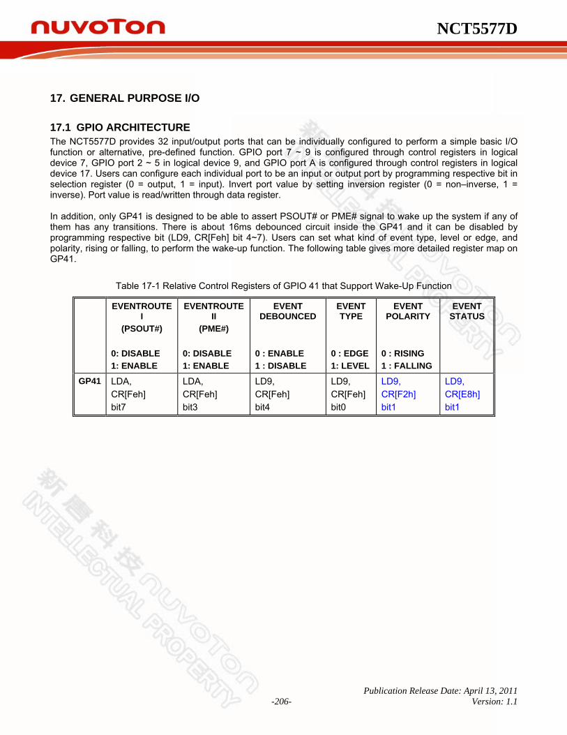
NCT5577D
Publication Release Date: April 13, 2011 -206- Version: 1.1
17. GENERAL PURPOSE I/O
17.1 GPIO ARCHITECTURE The NCT5577D provides 32 input/output ports that can be individually configured to perform a simple basic I/O function or alternative, pre-defined function. GPIO port 7 ~ 9 is configured through control registers in logical device 7, GPIO port 2 ~ 5 in logical device 9, and GPIO port A is configured through control registers in logical device 17. Users can configure each individual port to be an input or output port by programming respective bit in selection register (0 = output, 1 = input). Invert port value by setting inversion register (0 = non–inverse, 1 = inverse). Port value is read/written through data register. In addition, only GP41 is designed to be able to assert PSOUT# or PME# signal to wake up the system if any of them has any transitions. There is about 16ms debounced circuit inside the GP41 and it can be disabled by programming respective bit (LD9, CR[Feh] bit 4~7). Users can set what kind of event type, level or edge, and polarity, rising or falling, to perform the wake-up function. The following table gives more detailed register map on GP41.
Table 17-1 Relative Control Registers of GPIO 41 that Support Wake-Up Function
EVENTROUTE I
(PSOUT#)
0: DISABLE 1: ENABLE
EVENTROUTE II
(PME#)
0: DISABLE 1: ENABLE
EVENT DEBOUNCED
0 : ENABLE 1 : DISABLE
EVENT TYPE
0 : EDGE1: LEVEL
EVENT POLARITY
0 : RISING 1 : FALLING
EVENT STATUS
GP41 LDA, CR[Feh] bit7
LDA, CR[Feh] bit3
LD9, CR[Feh] bit4
LD9, CR[Feh] bit0
LD9, CR[F2h] bit1
LD9, CR[E8h] bit1

NCT5577D
Publication Release Date: April 13, 2011 -207- Version: 1.1
17.2 ACCESS CHANNELS There are two different channels to set up/access the GPIO ports. The first one is the indirect access via register 2E/2F (4E/4F, it depends by HEFRAS trapping). The registers can be read / written only when the respective logical device ID and port number are selected.
The other is the direct access through GPIO register table that can be configured by {CR61, CR60} of logic device 8. The mapped 5 registers are defined in table 17-2. Since the base address is set, the GPIO number can be selected by writing the group number to GSR [INDEX] (GPIO Select Register, #0~#A for GPIO2 ~ GPIOA respectively). Then the I/O register, the Data register and the Inversion register are mapped to addresses Base+0, Base+1 and Base+2 respectively. Only one GPIO can be accessed at one time.
Table 17-2 GPIO Register Addresses
BIT NUMBER ADDRESS ABBR 7 6 5 4 3 2 1 0
Base + 0 GSR Reserved INDEX Base + 1 IOR GPIO I/O Register Base + 2 DAT GPIO Data Register Base + 3 INV GPIO Inversion Register Base + 4 DST GPIO Status Register

NCT5577D
Publication Release Date: April 13, 2011 -208- Version: 1.1
18. SMBUS MASTER INTERFACE
18.1 General Description The SMBus interface module is two wire serial interface compatible to the SMBus physical layer. It is also compatible with Intel’s SMBus and Philips’ I2C bus. The rest of this section introduces the various features of the SMBus master capability. These features are divided into the following sections:
SMBus and I2C compliant AMD-TSI PCH SMBus master
18.2 Introduction to the SMBus Master
18.2.1 Data Transfer Format Every byte transferred on the bus consists of 8 bits. After the start condition, the master places the 7-bit address to the slave device it wants to address on the bus. The address followed an eight bit indicating the direction of the data transfer (R/W#); a zero indicates a transmission for data while a one indicates a request for data. Each byte is transferred with the most significant bit first, and after each byte, an acknowledge signal must follow. A data transfer is always terminated by stop condition generated by master.
Figure 18-1 Data Transfer Format
18.2.2 Arbitration Arbitration takes place on the SMBDAT data line while the SMBCLK line is high. Two devices may generate a start condition at the same time and enter the arbitration procedure. Arbitration continues until one master generates a HIGH level on the SMBDAT line while another competing master generates a LOW level on the SMBDAT line while SMBCLK is high. The master device which generated the HIGH level on SMBDAT loses arbitration. If a device loses arbitration during the first byte following a start condition i.e. while transmitting a slave address it becomes a slave receiver and monitors the address for a potential match. Arbitration may also be lost in the master receive mode during the acknowledge cycle.
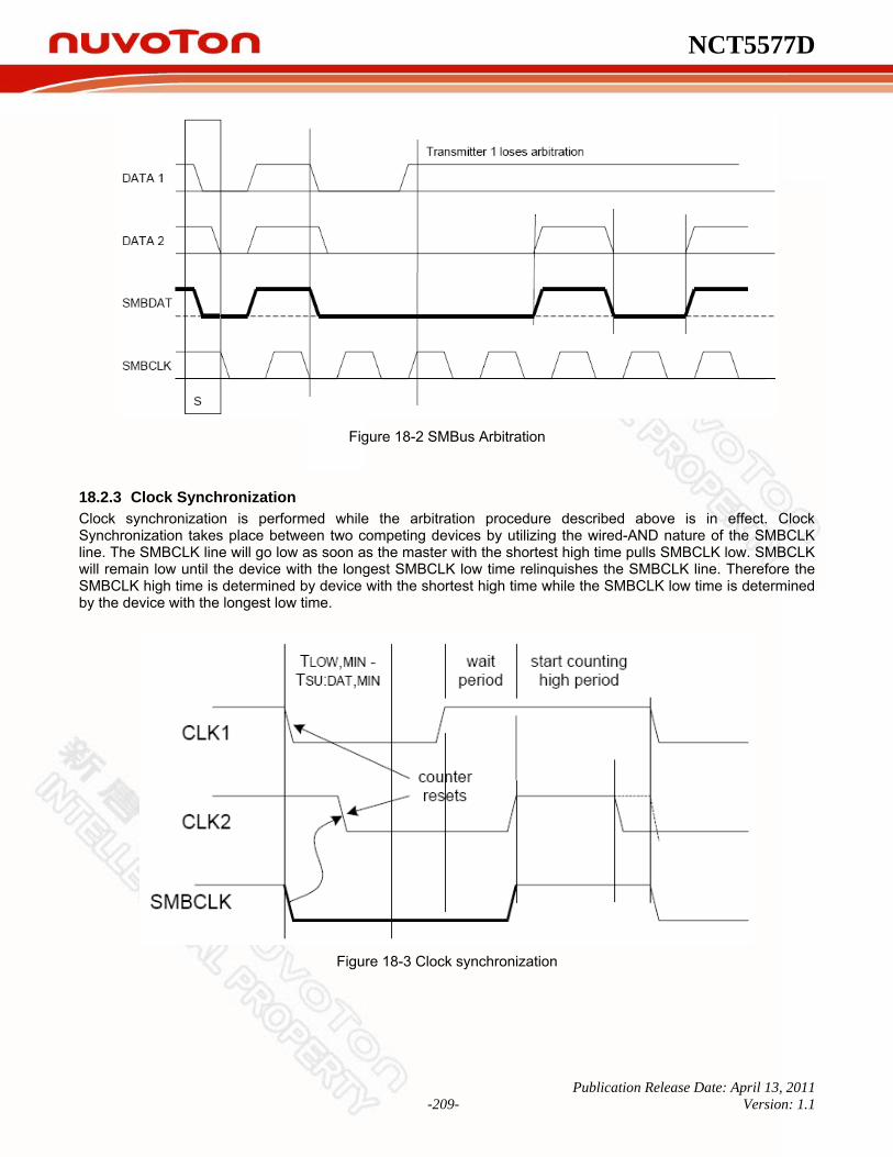
NCT5577D
Publication Release Date: April 13, 2011 -209- Version: 1.1
Figure 18-2 SMBus Arbitration
18.2.3 Clock Synchronization Clock synchronization is performed while the arbitration procedure described above is in effect. Clock Synchronization takes place between two competing devices by utilizing the wired-AND nature of the SMBCLK line. The SMBCLK line will go low as soon as the master with the shortest high time pulls SMBCLK low. SMBCLK will remain low until the device with the longest SMBCLK low time relinquishes the SMBCLK line. Therefore the SMBCLK high time is determined by device with the shortest high time while the SMBCLK low time is determined by the device with the longest low time.
Figure 18-3 Clock synchronization

NCT5577D
Publication Release Date: April 13, 2011 -210- Version: 1.1
18.3 SB-TSI The combined-format repeated start sequence is not supported in standard-mode and fast-mode.
Only 7-bit SMBus addresses are supported. SB-TSI implements the Send/Receive Byte and Read/Write Byte protocols. SB-TSI registers can only by written using a write byte command. Address Resolution Protocol (ARP) is not implemented. Packet Error Checking (PEC) is not supported.
18.3.1 SB-TSI Address The SMBus address is really 7 bits. The SB-TSI address is normally 98h or 4Ch. The address could vary with address select bits.
Table 18-1 SB-TSI Address Encoding
Address Select Bits SB-TSI Address
000b 98h
001b 9Ah
010b 9Ch
011b 9Eh
100b 90h
101b 92h
110b 94h
111b 96h
18.4 PCH The PCH provide system thermal data to EC. The EC can manage the fans and other cooling elements based on this data. A subset of the thermal collection is that the PCH and be programmed to alert the EC when a device has gone outside of its temperature limits.
18.4.1 Command Summary Table 18-2 PCH Command Summary
Trans-action Slave Addr.
Data Byte 0 =Com mand
Data Byte 1 =Byte Count
Data Byte 2
Data Byte 3
Data Byte 4
Data Byte 5
Data Byte 6
Data Byte 7
Write STS Preferences
I2C 0x41 0x6 STS [47:40]
STS [39:32]
STS [31:24]
STS [23:16]
STS [15:8]
STS [7:0]
Write CPU Temp Limits
I2C 0x42 0x6 Lower Limit [15:8]
Lower Limit [7:0]
Upper Limit [15:8]
Upper Limit [15:8]
Write MCH I2C 0x43 0x2 Lower Upper na na

NCT5577D
Publication Release Date: April 13, 2011 -211- Version: 1.1
I2C Module
Packet FSM
IIC FSM
INT
SMRDCNTSMBCMD SMBADDR
SMBCTL SMCTL2SMWRCNT
PCHADDR
SMCTL3 ACBCTL CFG
DAT_AVIL
F-Full
MU_SET
Scl in Sda_in
SCL OUT
SDA OUT
DAT_EN
DAT_OUT
CRC8 G/C
LPC
DAT
CS
WE#
RE#
Temp Limits Limit [7:0] Limit [7:0]
Write IBX Temp Limits
I2C 0x44 0x2 Lower Limit [7:0]
Upper Limit [7:0] na na
Write DIMM Temp Limits
I2C 0x45 0x2 Lower Limit [7:0]
Upper Limit [7:0] na na
Write MPC CPU Power
Clamp
I2C 0x50 0x2 Lower Limit [7:0]
Power Clamp [7:0]
Block Read Block Read Address
0x40 Block Read Address
Byte Count
Data 0 Data N PEC (optional)
18.5 SMBus Master
18.5.1 Block Diagram
Figure 18-4 SMBus Master Block Diagram
.
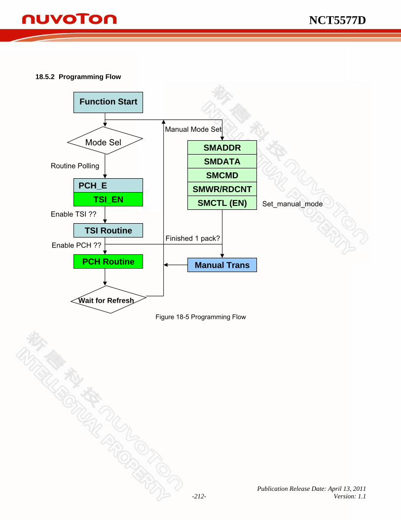
NCT5577D
Publication Release Date: April 13, 2011 -212- Version: 1.1
Function Start
PCH_E
TSI_EN
Routine Polling
Mode Sel
TSI Routine
PCH Routine
Enable TSI ??
Enable PCH ??
Wait for Refresh
Manual Mode Set
SMADDR SMDATA
SMWR/RDCNTSMCTL (EN)
Manual Trans
SMCMD
Finished 1 pack?
Set_manual_mode
18.5.2 Programming Flow
Figure 18-5 Programming Flow
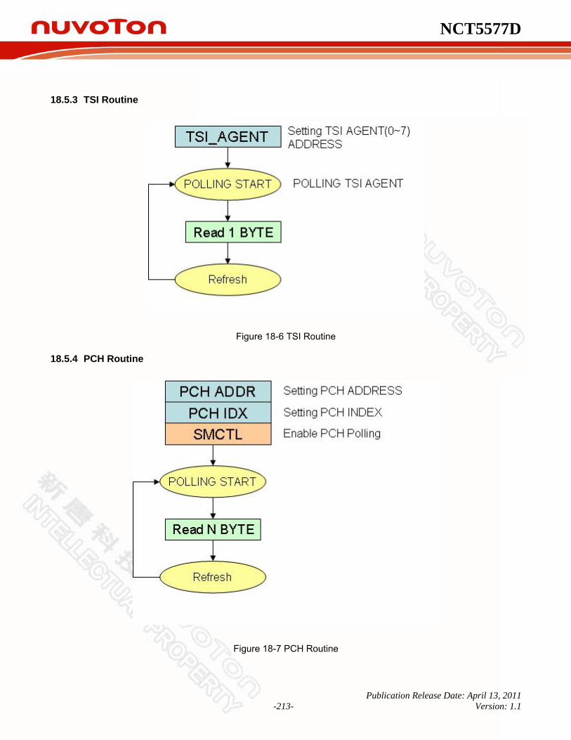
NCT5577D
Publication Release Date: April 13, 2011 -213- Version: 1.1
18.5.3 TSI Routine
Figure 18-6 TSI Routine
18.5.4 PCH Routine
Figure 18-7 PCH Routine
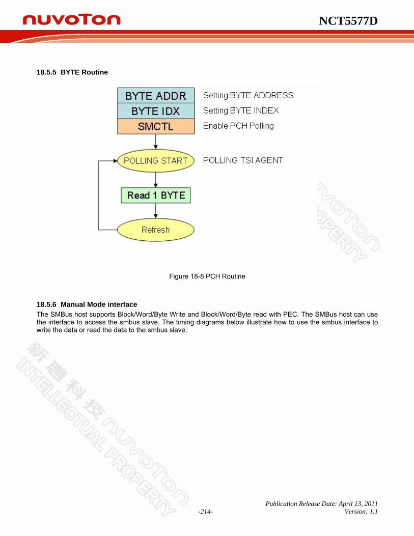
NCT5577D
Publication Release Date: April 13, 2011 -214- Version: 1.1
18.5.5 BYTE Routine
Figure 18-8 PCH Routine
18.5.6 Manual Mode interface The SMBus host supports Block/Word/Byte Write and Block/Word/Byte read with PEC. The SMBus host can use the interface to access the smbus slave. The timing diagrams below illustrate how to use the smbus interface to write the data or read the data to the smbus slave.

NCT5577D
Publication Release Date: April 13, 2011 -215- Version: 1.1
Figure 18-9 Manual Mode Programming Flow
18.6 Register Type Abbreviations The following abbreviations are used to indicate the Register Type:
R/W = Read/Write.
R = Read from register.
W = Write.
RO = Read-only.
To program the SMBus master configuration registers, the following configuration procedures must be followed in sequence: (1). Enter the Extended Function Mode. (2). Configure the configuration registers.
18.6.1 Enter the Extended Function Mode To place the chip into the Extended Function Mode, two successive writes of 0x26 must be applied to Extended Function Enable Registers (EFERs, i.e. 2Eh or 4Eh).

NCT5577D
Publication Release Date: April 13, 2011 -216- Version: 1.1
18.6.2 Configure the Configuration Registers The chip selects the Logical Device and activates the desired Logical Devices through Extended Function Index Register (EFIR) and Extended Function Data Register (EFDR). The EFIR is located at the same address as the EFER, and the EFDR is located at address (EFIR+1). First, write the Logical Device Number (i.e. 0x07) to the EFIR and then write the number of the desired Logical Device to the EFDR. If accessing the Chip (Global) Control Registers, this step is not required. Secondly, write the address of the desired configuration register within the Logical Device to the EFIR and then write (or read) the desired configuration register through the EFDR.
18.7 SMBus Master Register Set
18.7.1 SMBus Register Map SMBus Master base address in register Logic Device B CR62h(MSB), CR63h(LSB).
Table 18-3 SMBus Master Bank 0 Registers
Offset Type Name Section
0 R/W SMDATA 18.7.2
1 R/W SMWRSIZE 18.7.3
2 R/W SMBCMD 18.7.4
3 R/W SMIDX 18.7.5
4 R/W SMCTL 18.7.6
5 R/W SMADDR 18.7.7
6 R/W SCKFREQ 18.7.8
7 RO Reserved --
8 R/W PCHADDR 18.7.10
9 R/W Error_status 18.7.11
A R/W Reserved --
B R/W PCHCMD 18.7.13
D R/W TSI_AGENT --
E R/W SMCTL3 18.7.15
F R/W SMCTL2 18.7.15
10 R/W BYTE_ADDR
11 R/W BYTE_IDX_H
12 R/W BYTE_IDX_L
13 R/W Reserved
14 R/W Reserved

NCT5577D
Publication Release Date: April 13, 2011 -217- Version: 1.1
18.7.2 SMBus Data (SMDATA) – Bank 0 This 32 bits register is the data in and out register of SMBus data register. Before writing to SMDATA register, this register
contains the input data, after writing to SMDATA register, this register contains the output data.
Offset: 0h
Type: R/W
Byte 3 2 1 0 Name SMFIFO3 SMFIFO2 SMFIFO1 SMFIFO0 Default 00h 00h 00h 00h
Byte
Description 3 SMFIFO3 (SMBus FIFO 3). This byte represents the high byte of the 32 bits SMBus data.
2 SMFIFO2 (SMBus FIFO 2). This byte represents the second byte of the 32 bits SMBus data.
1 SMFIFO1 (SMBus FIFO 1). This byte represents the first byte of the 32 bits SMBus data.
0 SMFIFO0 (SMBus FIFO 0). This byte represents the low byte of the 32 bits SMBus data.
18.7.3 SMBus Write Data Size (SMWRSIZE) – Bank 0 Offset: 1h
Type: R/W Bit 7 6 5 4 3 2 1 0 Name Reserved SMWRSIZE Default 0 0 0 0 0 0 0 0
Bit
Description
7-5 Reserved.
4-0 SMWRSIZE (SMBus Write Byte Counter). This field sets the write byte counter, the max counter size is 32 bytes, and the minimal size is 1 bytes.
18.7.4 SMBus Command (SMCMD) – Bank 0 Offset: 2h
Type: R/W Bit 7 6 5 4 3 2 1 0 NAME REV SMBus CMD
Default 0 0 0 0 0 0 0 0
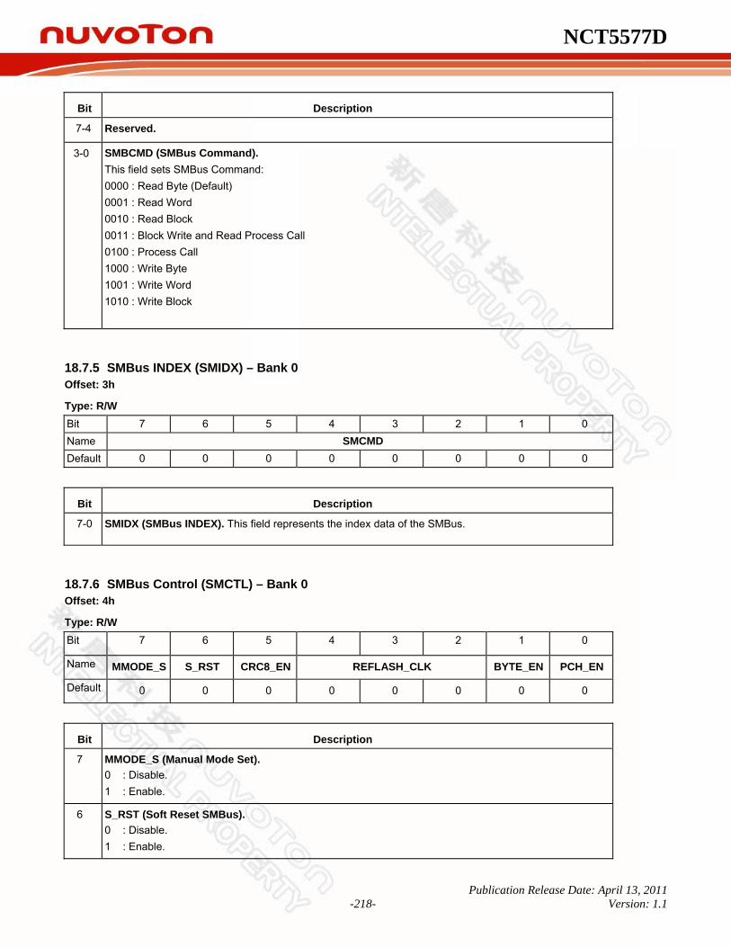
NCT5577D
Publication Release Date: April 13, 2011 -218- Version: 1.1
Bit
Description
7-4 Reserved.
3-0 SMBCMD (SMBus Command). This field sets SMBus Command: 0000 : Read Byte (Default) 0001 : Read Word 0010 : Read Block 0011 : Block Write and Read Process Call 0100 : Process Call 1000 : Write Byte 1001 : Write Word 1010 : Write Block
18.7.5 SMBus INDEX (SMIDX) – Bank 0 Offset: 3h
Type: R/W Bit 7 6 5 4 3 2 1 0 Name SMCMD Default 0 0 0 0 0 0 0 0
Bit
Description 7-0 SMIDX (SMBus INDEX). This field represents the index data of the SMBus.
18.7.6 SMBus Control (SMCTL) – Bank 0 Offset: 4h
Type: R/W Bit 7 6 5 4 3 2 1 0
Name MMODE_S S_RST CRC8_EN REFLASH_CLK BYTE_EN PCH_EN
Default 0 0 0 0 0 0 0 0
Bit
Description 7 MMODE_S (Manual Mode Set).
0 : Disable. 1 : Enable.
6 S_RST (Soft Reset SMBus). 0 : Disable. 1 : Enable.

NCT5577D
Publication Release Date: April 13, 2011 -219- Version: 1.1
5 CRC8_EN (CRC8 Enable). 0 : CRC8 function is disable. 1 : CRC8 function is enable.
4-2 REFRASH_CLK (Refrash Clock Select). 000, 100 – 128ms 001, 101 – 256ms 010, 110 – 512ms 011, 111 – 64ms (1KHz)
1 BYTE_EN (BYTE Enable). 0 : BYTE function is disable. 1 : BYTE function is enable.
0 PCH_EN (PCH Enable). 0 : PCH function is disable. 1 : PCH function is enable.
18.7.7 SMBus Address (SMADDR) – Bank 0 Offset: 5h
Type: R/W Bit 7 6 5 4 3 2 1 0
Name SMADDR REV
Default 0 0 0 0 0 0 0 0
Bit
Description 7-1 SMADDR (SMBus Address). AMD-TSI only supports 7-bit SMBus address.
0 Reserved: 0 : Write. If the protocol is write, the WR_SIZE can’t be zero. (Default)
18.7.8 ACB Control 2 (ACBCTRL2) – Bank 0 Offset: 6h
Type: R/W Bit 7 6 5 4 3 2 1 0
Reserved: SCLFREQ Default 0 0 0 0 0 1 1 1
Bit
Description 7-4 Reserved

NCT5577D
Publication Release Date: April 13, 2011 -220- Version: 1.1
3-0 SCLFQ (SMBCLK Frequency). This field defines the SMBCLK period (low time and high time). The clock low time and high time ate defined as follows: 0000 : 382KHz
0001 : 266KHz 0010 : 204KHz
0011 : 165KHz
0100 : 139KHz
0101 : 120KHz
0110 : 105KHz
0111 : 94KHz (Default)
1000 : 85KHz
1001 : 77KHz
1010 : 71KHz
1011 : 65KHz
1100 : 61KHz
1101 : 57KHz
1110 : 53KHz
1111 : 48KHz
18.7.9 PCH Address (PCHADDR) – Bank 0 Offset: 8h
Type: R/W Bit 7 6 5 4 3 2 1 0 Name PCHADDR REV Default 1 0 0 1 0 1 0 0
Bit
Description 7-1 PCHADDR (PCH Address). PCH supports 8-bit SMBus address. The default address is 94h. The last bit
is read or write bit. It needs to set to “0”.
18.7.10 SMBus Error Status (Error_status) – Bank 0 Offset: 9h
Type: RO/W1C Bit 7 6 5 4 3 2 1 0
Name REV ADNACK Timeout Reserved BER NACK Reserved
Default 1 0 0 1 0 1 0 0
Bit
Description
7-6 Reserved.
5 ADDR Non ACK. This bit reflects SMBus occurred ADDRESS NON ACK in Manual mode..
4 Timeout. This bit reflects when SMBus occurs timeout.

NCT5577D
Publication Release Date: April 13, 2011 -221- Version: 1.1
3 Reserved.
2 BER (Bus Error). This bit reflects when a start or stop condition is detected during data transfer, or when an arbitration problem is detected.
1 NACK (Negative acknowledge). This bit is set by hardware when a transmission is not acknowledged on the ninth clock. While NACK is set SCL will be drive low and subsequent bus transactions are stalled until NACK is cleared.
0 Reserved.
18.7.11 PCH Command (PCHCMD) – Bank 0 Offset: bh
Type: R/W Bit 7 6 5 4 3 2 1 0 Name PCHCMD Default 0 1 0 0 0 0 0 0
Bit
Description 7-0 PCHCMD (PCH Command).
This field represents the command data of the PCH. The default command is block read (40h).
18.7.12 TSI Agent Enable Register (TSI_AGENT) – Bank Offset: dh
Type: RO Bit 7 6 5 4 3 2 1 0
Name AG7 AG6 AG5 AG4 AG3 AG2 AG1 AG0
Default 0 0 0 0 0 0 0 0
Bit
Description
7 TSI AGENT7 Enable. : This bit reflects AMD-TSI Agent enbale. 0 : Diable
6 TSI AGENT6 Enable. : This bit reflects AMD-TSI Agent enbale. 0 : Diable
5 TSI AGENT5 Enable. : This bit reflects AMD-TSI Agent enbale. 0 : Diable
4 TSI AGENT4 Enable. : This bit reflects AMD-TSI Agent enbale. 0 : Diable

NCT5577D
Publication Release Date: April 13, 2011 -222- Version: 1.1
3 TSI AGENT3 Enable. : This bit reflects AMD-TSI Agent enbale. 0 : Diable
2 TSI AGENT2 Enable. : This bit reflects AMD-TSI Agent enbale. 0 : Diable
1 TSI AGENT1 Enable. : This bit reflects AMD-TSI Agent enbale. 0 : Diable 1 : Full
0 TSI AGENT0 Enable. : This bit reflects AMD-TSI Agent enbale. 0 : Diable 1 : Empty
18.7.13 SMBus Control 3 Register (SMCTL3) – Bank 0 Offset: eh
Type: RO Bit 7 6 5 4 3 2 1 0 Name Reserved CRC_CHK M_MODE F_FULL F_EMPTDefault 0 0 0 0 0 0 0 0
Bit
Description
7-4 Reserved
3 CRC_CHK (CRC Check). 0 : incorrect 1 : correct
2 M_MODE (Manual Mode). 0 : Non-active 1 : Active
1 F_FULL (fifo_full). : This bit reflects SMBus data fifo is full. 0 : Non-full 1 : Full
0 F_EMPT (fifo empty). : This bit reflects the SMBus data fifo is empty. 0 : Non-empty 1 : Empty
18.7.14 SMBus Control 2 Register (SMCTL2) – Bank 0 Offset: fh
Type: R/W Bit 7 6 5 4 3 2 1 0
Name Reserved INT_LCH_E Reserved BYTE_SEL BANKSEL
Default 0 0 0 0 0 0 0 0
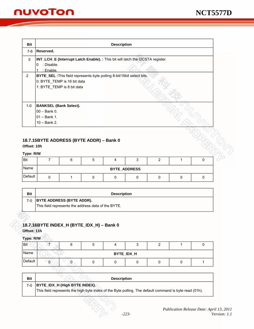
NCT5577D
Publication Release Date: April 13, 2011 -223- Version: 1.1
Bit
Description 7-6 Reserved.
5 INT_LCH_E (Interrupt Latch Enable). : This bit will latch the I2CSTA register. 0 : Disable. 1 : Enable.
2 BYTE_SEL :This field represents byte polling 8-bit/16bit select bits. 0: BYTE_TEMP is 16 bit data 1: BYTE_TEMP is 8 bit data
1-0 BANKSEL (Bank Select). 00 – Bank 0. 01 – Bank 1. 10 – Bank 2.
18.7.15 BYTE ADDRESS (BYTE ADDR) – Bank 0 Offset: 10h
Type: R/W Bit 7 6 5 4 3 2 1 0
Name BYTE_ADDRESS
Default 0 1 0 0 0 0 0 0
Bit
Description 7-0 BYTE ADDRESS (BYTE ADDR).
This field represents the address data of the BYTE.
18.7.16 BYTE INDEX_H (BYTE_IDX_H) – Bank 0 Offset: 11h
Type: R/W Bit 7 6 5 4 3 2 1 0
Name BYTE_IDX_H
Default 0 0 0 0 0 0 0 1
Bit
Description 7-0 BYTE_IDX_H (High BYTE INDEX).
This field represents the high byte index of the Byte polling. The default command is byte read (01h).

NCT5577D
Publication Release Date: April 13, 2011 -224- Version: 1.1
18.7.17 BYTE INDEX_L (BYTE_IDX_L) – Bank 0 Offset: 12h
Type: R/W Bit 7 6 5 4 3 2 1 0
Name BYTE_IDX_L
Default 0 0 0 1 0 0 0 0
Bit
Description 7-0 BYTE_IDX_L (LOW BYTE INDEX).
This field represents the low byte index of the Byte polling. The default command is byte read (10h).
The EC may read thermal information from IBX using the SMBus block read command. The IBX doesn’t support byte-read or word-read SMBus commands. The read use a different address that the writes. The address must be different so that the IBX knows which target Is intended, either the I2C target or the block read buffer. The IBX and EC are set up by BIOS with the length of the read that is supported by the platform. The EC must always do reads of the lengths set up by BIOS. There is no way to change the length of the read after BIOS has set things up. An EC that only wants the single highest temperature among MCH, and CPU could read one byte. A 2 byte read would provide both IBX and CPU/MCH package temperature. An EC that wanted each components temperature would do a 4 byte read. An EC that also wanted DIMM information would read 9 bytes. If an EC wanted to read the HOST STS status, it must read 19 bytes. An EC can also read the energy data provided by the CPU by reading 12 bytes.

NCT5577D
Publication Release Date: April 13, 2011 -225- Version: 1.1
19. CONFIGURATION REGISTER
19.1 Chip (Global) Control Register Default Value of Global Control Register: Register Default Register Default Register Default CR 10h FFh CR 21h 33h (ID_L) CR 2Bh 00h CR 11h FFh CR 22h FFh CR 2Ch 81h CR 13h 00h CR 24h 64h CR 2Dh 00h CR 14h 00h CR 25h 00h CR 2Fh 00ssssssbCR 1Ah F0h CR 26h 0s000000b CR 1Bh 78h CR 27h 00h CR 1Ch 00h CR 28h 00h CR 20h C3h (ID_H) CR 2Ah C0h Note. The value of “s” means hardware strapping result: strapping high will report 1; strapping low will report 0. In addition, BIOS can write the value of strapping result after hardware strapping. Reserved Registers of Global Control Register: Register Default Register Default CR 02h 00h CR 1Dh 00h CR 16h FFh CR 1Eh FFh CR 17h FFh CR 1Fh FFh CR 18h FFh CR 23h 00h CR 19h FFh CR 2Eh 00h Note. All reserved registers must keep default value. Note. Before accessing CR10, CR11, CR13 and CR14, CR26 [Bit4] must be set to logic 1. CR 02h. Reserved.Software Reset Register Attribute: Write Only Power Well: VCC Reset by: LRESET# Default : 00h CR 07h. Logical Device Selection Attribute: Read/Write Power Well: VCC Reset by: LRESET# Default : 00h
BIT READ / WRITE DESCRIPTION
7-0 R / W Logical Device Number.

NCT5577D
Publication Release Date: April 13, 2011 -226- Version: 1.1
CR 10h. Device IRQ TYPE Selection Location: Address 10h Attribute: Read/Write Power Well: VCC Reset by: LRESET# Default : FFh Size: 8 bits
BIT READ / WRITE DESCRIPTION
7~6 Reserved.
5 R / W UARTA IRQ TYPE SELECT (note1.) 0: Edge. 1: Level.
4 Reserved.
3 R / W KBC IRQ TYPE SELECT (note1.) 0: Edge. 1: Level.
2 R / W MOUSE IRQ TYPE SELECT (note1.) 0: Edge. 1: Level.
1 R / W CIR IRQ TYPE SELECT (note1.) 0: Edge. 1: Level.
0 R / W CIRWAKUP IRQ TYPE SELECT (note1.) 0: Edge. 1: Level.
Note1: Before accessing CR10, CR11, CR13 and CR14, CR26 [Bit4] must be set to logic 1. CR 11h. Device IRQ TYPE Selection Location: Address 11h Attribute: Read/Write Power Well: VCC Reset by: LRESET# Default : FFh Size: 8 bits
BIT READ / WRITE DESCRIPTION
7 R / W HM IRQ TYPE SELECT (note1.) 0: Edge. 1: Level.
6 R / W WDTO IRQ TYPE SELECT (note1.) 0: Edge. 1: Level.
5-2 Reserved.
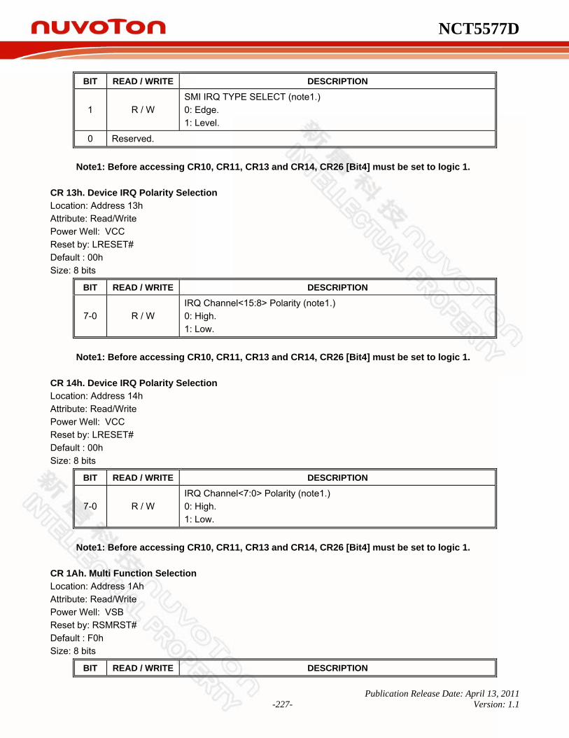
NCT5577D
Publication Release Date: April 13, 2011 -227- Version: 1.1
BIT READ / WRITE DESCRIPTION
1 R / W SMI IRQ TYPE SELECT (note1.) 0: Edge. 1: Level.
0 Reserved.
Note1: Before accessing CR10, CR11, CR13 and CR14, CR26 [Bit4] must be set to logic 1. CR 13h. Device IRQ Polarity Selection Location: Address 13h Attribute: Read/Write Power Well: VCC Reset by: LRESET# Default : 00h Size: 8 bits
BIT READ / WRITE DESCRIPTION
7-0 R / W IRQ Channel<15:8> Polarity (note1.) 0: High. 1: Low.
Note1: Before accessing CR10, CR11, CR13 and CR14, CR26 [Bit4] must be set to logic 1. CR 14h. Device IRQ Polarity Selection Location: Address 14h Attribute: Read/Write Power Well: VCC Reset by: LRESET# Default : 00h Size: 8 bits
BIT READ / WRITE DESCRIPTION
7-0 R / W IRQ Channel<7:0> Polarity (note1.) 0: High. 1: Low.
Note1: Before accessing CR10, CR11, CR13 and CR14, CR26 [Bit4] must be set to logic 1. CR 1Ah. Multi Function Selection Location: Address 1Ah Attribute: Read/Write Power Well: VSB Reset by: RSMRST# Default : F0h Size: 8 bits
BIT READ / WRITE DESCRIPTION
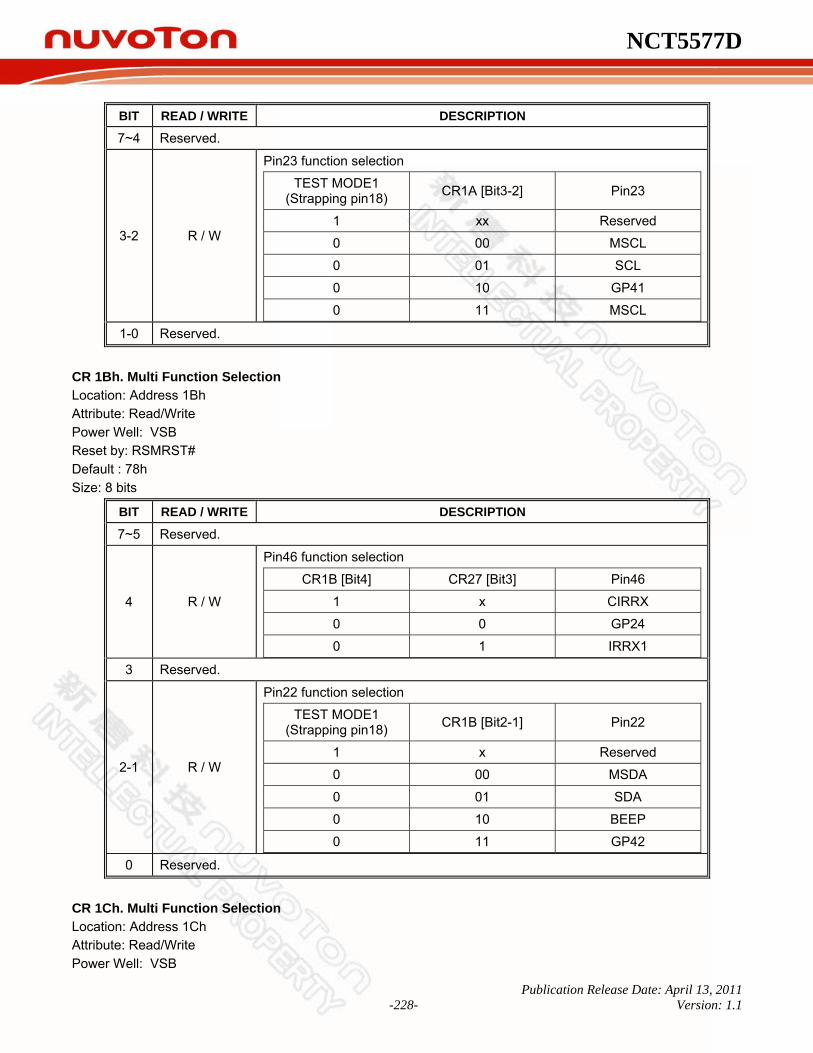
NCT5577D
Publication Release Date: April 13, 2011 -228- Version: 1.1
BIT READ / WRITE DESCRIPTION
7~4 Reserved.
3-2 R / W
Pin23 function selection
TEST MODE1 (Strapping pin18) CR1A [Bit3-2] Pin23
1 xx Reserved
0 00 MSCL
0 01 SCL
0 10 GP41
0 11 MSCL 1-0 Reserved.
CR 1Bh. Multi Function Selection Location: Address 1Bh Attribute: Read/Write Power Well: VSB Reset by: RSMRST# Default : 78h Size: 8 bits
BIT READ / WRITE DESCRIPTION
7~5 Reserved.
4 R / W
Pin46 function selection
CR1B [Bit4] CR27 [Bit3] Pin46
1 x CIRRX
0 0 GP24
0 1 IRRX1 3 Reserved.
2-1 R / W
Pin22 function selection
TEST MODE1 (Strapping pin18) CR1B [Bit2-1] Pin22
1 x Reserved
0 00 MSDA
0 01 SDA
0 10 BEEP
0 11 GP42 0 Reserved.
CR 1Ch. Multi Function Selection Location: Address 1Ch Attribute: Read/Write Power Well: VSB

NCT5577D
Publication Release Date: April 13, 2011 -229- Version: 1.1
Reset by: LRESET# Default : 00h Size: 8 bits
BIT READ / WRITE DESCRIPTION
7-0 Reserved.
CR 20h. Chip ID ( High Byte ) Attribute: Read Only Power Well: VCC Reset by: None Default : C3h
BIT READ / WRITE DESCRIPTION
7-0 Read Only Chip ID number = C3h (high byte).
CR 21h. Chip ID ( Low Byte ) Attribute: Read Only Power Well: VCC Reset by: None Default : 33h
BIT READ / WRITE DESCRIPTION
7-0 Read Only Chip ID number = 33h (low byte)
CR 22h. Device Power Down Location: Address 22h Attribute: Read/Write Power Well: VCC Reset by: LRESET# Default : FFh Size: 8 bits
BIT READ / WRITE DESCRIPTION
7-5 Reserved.
4 R / W UARTA Power Down. 0: Powered down. 1: Not powered down.
3-2 Reserved.
1 R / W IPD (Immediate Power Down). When set to 0, the whole chip is put into power-down mode immediately.
0 Reserved.
CR 24h. Global Option Location: Address 24h Attribute: Read/Write Power Well: VCC Reset by: LRESET# Default : 64h

NCT5577D
Publication Release Date: April 13, 2011 -230- Version: 1.1
Size: 8 bits
BIT READ / WRITE DESCRIPTION
7-5 Reserved.
4 R / W Select output type of SYSFANOUT =0 SYSFANOUT is Open-drain. (Default) =1 SYSFANOUT is Push-pull.
3 R / W Select output type of CPUFANOUT =0 CPUFANOUT is Open-drain. (Default) =1 CPUFANOUT is Push-pull.
2-1 Reserved.
0 R / W
PNPCVS => = 0 The compatible PNP address-select registers have default values.= 1 The compatible PNP address-select registers have no default values.
CR 25h. Interface Tri-state Enable Location: Address 25h Attribute: Read/Write Power Well: VCC Reset by: LRESET# Default : 00h Size: 8 bits
BIT READ / WRITE DESCRIPTION
7~3 Reserved.
2 R / W UARTATRI
1~0 Reserved.
CR 26h. Global Option s: value by strapping Location: Address 26h Attribute: Read/Write Power Well: VCC Reset by: LRESET# Default : 0s000000b Size: 8 bits
BIT READ / WRITE DESCRIPTION
7 Reserved.
6 R / W
HEFRAS => = 0 Write 87h to location 2E twice. = 1 Write 87h to location 4E twice. The corresponding power-on strapping pin is RTSA# (Pin 31).
5 R / W LOCKREG => = 0 Enable R/W configuration registers. = 1 Disable R/W configuration registers.

NCT5577D
Publication Release Date: April 13, 2011 -231- Version: 1.1
BIT READ / WRITE DESCRIPTION
4~2 Reserved.
1 R / W
DSUALGRQ => = 0 Enable UART A legacy mode for IRQ selection. Then HCR register (base address + 4) bit 3 is effective when selecting IRQ. = 1 Disable UART A legacy mode for IRQ selection. Then HCR register (base address + 4) bit 3 is not effective when selecting IRQ.
0 R / W
DSUBLGRQ => = 0 Enable IR legacy mode for IRQ selection. Then HCR register (base address + 4) bit 3 is effective when selecting IRQ. = 1 Disable IR legacy mode for IRQ selection. Then HCR register (base address + 4) bit 3 is not effective when selecting IRQ.
CR 27h. Global Option Location: Address 27h Attribute: Read/Write Power Well: VSB Reset by: RSMRST# Default : 00h Size: 8 bits
BIT READ / WRITE DESCRIPTION
7 R / W
Pin43 function selection
CR27 [Bit7] AMDPWR_EN (Strapping pin47)
CR2F [Bit3] Pin43
1 x x GP75
0 1 x Reserved
0 x 1 Reserved
0 0 0 SLP_SUS_FET
Pin44 function selection
CR27 [Bit7] AMDPWR_EN (Strapping pin47)
CR2F [Bit3] Pin44
1 x x GP74
0 1 x Reserved
0 x 1 Reserved
0 0 0 SLP_SUS#

NCT5577D
Publication Release Date: April 13, 2011 -232- Version: 1.1
BIT READ / WRITE DESCRIPTION
6 R / W
Pin41 function selection
CR27 [Bit6] AMDPWR_EN (Strapping pin47)
Pin41
1 x GP77
0 0 Reserved
0 1 VLDT_EN
Pin42 function selection
CR27 [Bit6] AMDPWR_EN (Strapping pin47)
Pin42
1 x GP76
0 0 Reserved
0 1 VCORE_EN 5~4 Reserved.
3 R / W
Pin46 function selection
CR1B [Bit4] CR27 [Bit3] Pin46
1 x CIRRX (Default)
0 0 GP24
0 1 IRRX1
Pin47 function selection
CR2A [Bit3] CR27 [Bit3] Pin47
1 x CIRTX1
0 0 GP25 (Default)
0 1 IRTX1 2 Reserved.
1 R / W LV_DETECT_L 0: AMD power sequence detect level and time delay 1: AMD power sequence non detect level but time delay
0 Reserved.
CR 28h. Global Option Location: Address 28h Attribute: Read/Write Power Well: VCC Reset by: LRESET# Default : 00h Size: 8 bits
BIT READ / WRITE DESCRIPTION
7-0 Reserved.
CR 2Ah. Multi Function Selection
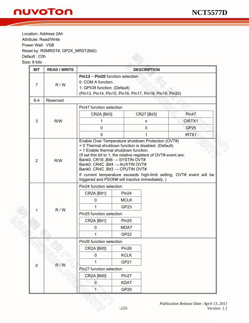
NCT5577D
Publication Release Date: April 13, 2011 -233- Version: 1.1
Location: Address 2Ah Attribute: Read/Write Power Well: VSB Reset by: RSMRST#, GP2X_MRST(Bit0) Default : C0h Size: 8 bits
BIT READ / WRITE DESCRIPTION
7 R / W
Pin13 ~ Pin20 function selection 0: COM A function. 1: GPIO8 function. (Default) (Pin13, Pin14, Pin15, Pin16, Pin17, Pin18, Pin19, Pin20)
6-4 Reserved.
3 R/W
Pin47 function selection
CR2A [Bit3] CR27 [Bit3] Pin47
1 x CIRTX1
0 0 GP25
0 1 IRTX1
2 R/W
Enable Over Temperature shutdown Protection (OVT#) = 0 Thermal shutdown function is disabled. (Default) = 1 Enable thermal shutdown function. (If set this bit to 1, the relative registers of OVT# event are: Bank0, CR18 ,Bit6 → SYSTIN OVT# Bank0, CR4C ,Bit4 → AUXTIN OVT# Bank0, CR4C ,Bit3 → CPUTIN OVT# If current temperature exceeds high-limit setting, OVT# event will be triggered and PSON# will inactive immediately. )
1 R / W
Pin24 function selection
CR2A [Bit1] Pin24
0 MCLK
1 GP23
Pin25 function selection
CR2A [Bit1] Pin25
0 MDAT
1 GP22
0 R / W
Pin26 function selection
CR2A [Bit0] Pin26
0 KCLK
1 GP21
Pin27 function selection
CR2A [Bit0] Pin27
0 KDAT
1 GP20

NCT5577D
Publication Release Date: April 13, 2011 -234- Version: 1.1
CR 2Bh. Multi Function Selection Location: Address 2Bh Attribute: Read/Write Power Well: VSB Reset by: RSMRST# Default : 00h Size: 8 bits
BIT READ / WRITE DESCRIPTION
7 Reserved.
6 R / W
Pin35 function selection
CR2B [Bit6] Pin35
0 RSTOUT1#
1 GP36
5 R / W
Pin36 function selection
CR2B [Bit5] Pin36
0 RSTOUT0#
1 GP35
4 R / W
Pin37 function selection
CR2B [Bit4] Pin37
0 ATXPGD
1 GP34
3 R / W
Pin38 function selection
CR2B [Bit3] Pin38
0 CPUPWRGD
1 GP33
2 R / W
Pin39 function selection
CR2B [Bit2] Pin39
0 PWROK
1 GP32
1 Reserved.
0 R / W
Pin40 function selection
CR2B [Bit0] Pin40
0 SLP_S5#
1 GP30 CR 2Ch. Multi Function Selection Location: Address 2Ch Attribute: Read/Write Power Well: VSB
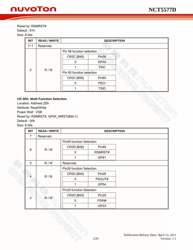
NCT5577D
Publication Release Date: April 13, 2011 -235- Version: 1.1
Reset by: RSMRST# Default : 81h Size: 8 bits
BIT READ / WRITE DESCRIPTION
7~1 Reserved.
0 R / W
Pin 58 function selection
CR2C [Bit5] Pin58
0 GPA0
1 TSIC
Pin 60 function selection
CR2C [Bit5] Pin60
0 PECI
1 TSID CR 2Dh. Multi Function Selection Location: Address 2Dh Attribute: Read/Write Power Well: VSB Reset by: RSMRST#, GP5X_MRST(Bit4-1) Default : 00h Size: 8 bits
BIT READ / WRITE DESCRIPTION
7 Reserved.
6 R / W
Pin49 function Selection
CR2D [Bit6] Pin49
0 RSMRST#
1 GP91 5 R / W Reserved.
4 R / W
Pin28 function Selection
CR2D [Bit4] Pin28
0 PSOUT#
1 GP54
3 R / W
Pin29 function Selection
CR2D [Bit3] Pin29
0 PSIN#
1 GP53

NCT5577D
Publication Release Date: April 13, 2011 -236- Version: 1.1
BIT READ / WRITE DESCRIPTION
2 R / W
Pin30 function Selection
CR2D [Bit2] AMDPWR_EN Pin30
1 x GP52
0 0 PSON#
0 1 AMD_PSON#
1 R / W
Pin31 function Selection
CR2D [Bit3] Pin31
0 SLP_S3#
1 GP51 0 Reserved.
CR 2Fh. Strapping Function Result Location: Address 2Fh Attribute: Read/Write Power Well: VSB Reset by: RSMRST#(Bit5-2), PWROK(Bit1-0) Default : by 00ss_ssss Size: 8 bits
BIT READ / WRITE DESCRIPTION
7-6 Reserved.
5 R/W AMDPWR_EN Strapping result reading
4-2 Reserved.
1 R / W TEST MODE1 Strapping result reading
0 R / W 24M_48M_SEL Strapping result reading
Note . All Strapping results can be programming by LPC Interface. There are three conditions below: 3) VSB Strapping result can be programming by LPC, and reset by RSMRST# 4) VCC Strapping result can be programming by LPC, and reset by PWROK 5) LRESET Strapping (2E_4E_SEL) : No change

NCT5577D
Publication Release Date: April 13, 2011 -237- Version: 1.1
19.2 Logical Device 2 (UART A) CR 30h. Attribute: Read/Write Power Well: VCC Reset by: LRESET# Default : 01h
BIT READ / WRITE DESCRIPTION
7-1 Reserved.
0 R / W 0: The logical device is inactive. 1: The logical device is active.
CR 60h, 61h. Attribute: Read/Write Power Well: VCC Reset by: LRESET# Default : 03h, F8h
BIT READ / WRITE DESCRIPTION
7-0 R / W These two registers select Serial Port 1 I/O base address <100h: FF8h> on 8 bytes boundary.
CR 70h. Attribute: Read/Write Power Well: VCC Reset by: LRESET# Default : 04h
BIT READ / WRITE DESCRIPTION
7-4 Reserved.
3-0 R / W These bits select IRQ resource for Serial Port 1.
CR F0h. Attribute: Read/Write Power Well: VCC Reset by: LRESET# Default : 00h
BIT READ / WRITE DESCRIPTION
7 R / W 0: Delay RXCLK for 5 ns for LG issue. 1: No delay of 5 ns for RXCLK.
6 R / W 0: IRQ is the level mode. 1: IRQ is the pulse mode for IRQ sharing function.
5 R / W 0: Using the original RX FIFO Error Indication signal (USR bit 7). 1: Using new RX FIFO Error Indication signal to solve some issues.
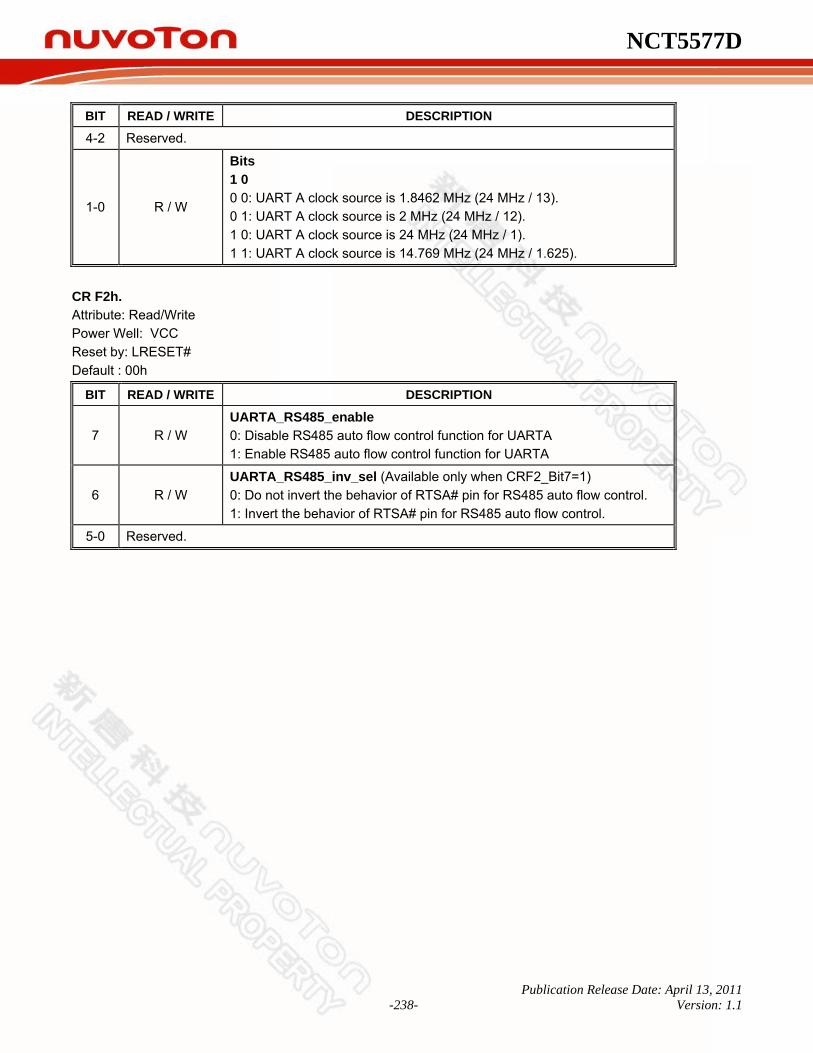
NCT5577D
Publication Release Date: April 13, 2011 -238- Version: 1.1
BIT READ / WRITE DESCRIPTION
4-2 Reserved.
1-0 R / W
Bits 1 0 0 0: UART A clock source is 1.8462 MHz (24 MHz / 13). 0 1: UART A clock source is 2 MHz (24 MHz / 12). 1 0: UART A clock source is 24 MHz (24 MHz / 1). 1 1: UART A clock source is 14.769 MHz (24 MHz / 1.625).
CR F2h. Attribute: Read/Write Power Well: VCC Reset by: LRESET# Default : 00h
BIT READ / WRITE DESCRIPTION
7 R / W UARTA_RS485_enable 0: Disable RS485 auto flow control function for UARTA 1: Enable RS485 auto flow control function for UARTA
6 R / W UARTA_RS485_inv_sel (Available only when CRF2_Bit7=1) 0: Do not invert the behavior of RTSA# pin for RS485 auto flow control. 1: Invert the behavior of RTSA# pin for RS485 auto flow control.
5-0 Reserved.

NCT5577D
Publication Release Date: April 13, 2011 -239- Version: 1.1
19.3 Logical Device 3 (IR) CR 30h. Location: Address 30h Attribute: Read/Write Power Well: VCC Reset by: LRESET# Default : 01h Size: 8 bits
BIT READ / WRITE DESCRIPTION
7~1 Reserved.
0 R / W 0: The logical device is inactive. 1: The logical device is active.
CR 60h, 61h. Location: Address 60h, 61h Attribute: Read/Write Power Well: VCC Reset by: LRESET# Default : 02h, F8h Size: 16 bits
BIT READ / WRITE DESCRIPTION
7~0 R / W These two registers select IR I/O base address <100h: FF8h> on eight-byte boundary.
CR 70h. Location: Address 70h Attribute: Read/Write Power Well: VCC Reset by: LRESET# Default : 03h Size: 8 bits
BIT READ / WRITE DESCRIPTION
7~4 Reserved.
3~0 R / W These bits select IRQ resource for IR.
CR F0h. Location: Address F0h Attribute: Read/Write Power Well: VCC Reset by: LRESET# Default : 00h Size: 8 bits

NCT5577D
Publication Release Date: April 13, 2011 -240- Version: 1.1
BIT READ / WRITE DESCRIPTION
7 R / W 0: Delay RXCLK for 5 ns for LG issue. 1: No delay of 5 ns for RXCLK.
6 R / W 0: IRQ is the level mode. 1: IRQ is the pulse mode for IRQ sharing function.
5 R / W 0: Using the original RX FIFO Error Indication signal (USR bit 7). 1: Using new RX FIFO Error Indication signal to solve some issues.
4~2 Reserved.
1~0 R / W
Bits 1 0 0 0: IR clock source is 1.8462 MHz (24 MHz / 13). 0 1: IR clock source is 2 MHz (24 MHz / 12). 0 0: IR clock source is 24 MHz (24 MHz / 1). 1 1: IR clock source is 14.769 MHz (24 MHz / 1.625).
CR F1h. Location: Address F1h Attribute: Read/Write Power Well: VCC Reset by: LRESET# Default : 00h Size: 8 bits
BIT READ / WRITE DESCRIPTION
7 Reserved.
6 R / W IRLOCSEL => IR I/O pins’ location selection. 0: reserved. 1: Through IRRX / IRTX.
5~3 R / W IRMODE => IR function mode selection. See the table below.
2 R / W IR half / full duplex function selection. 0: IR function is Full Duplex. 1: IR function is Half Duplex.
1 R / W 0: IRTX pin of IR function in normal condition. 1: Inverse IRTX pin of IR function.
0 R / W 0: IRRX pin of IR function in normal condition. 1: Inverse IRRX pin of IR function.
IR MODE IR FUNCTION IRTX IRRX
00X Disable Tri-state High
010* IrDA Active pulse 1.6 μS Demodulation into SINB/IRRX
011* IrDA Active pulse 3/16 bit time Demodulation into SINB/IRRX
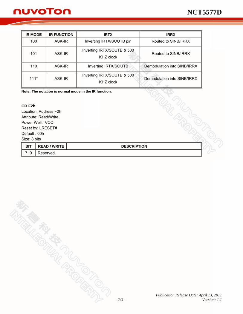
NCT5577D
Publication Release Date: April 13, 2011 -241- Version: 1.1
IR MODE IR FUNCTION IRTX IRRX
100 ASK-IR Inverting IRTX/SOUTB pin Routed to SINB/IRRX
101 ASK-IR Inverting IRTX/SOUTB & 500
KHZ clock Routed to SINB/IRRX
110 ASK-IR Inverting IRTX/SOUTB Demodulation into SINB/IRRX
111* ASK-IR Inverting IRTX/SOUTB & 500
KHZ clock Demodulation into SINB/IRRX
Note: The notation is normal mode in the IR function.
CR F2h. Location: Address F2h Attribute: Read/Write Power Well: VCC Reset by: LRESET# Default : 00h Size: 8 bits
BIT READ / WRITE DESCRIPTION
7~0 Reserved.

NCT5577D
Publication Release Date: April 13, 2011 -242- Version: 1.1
19.4 Logical Device 5 (Keyboard Controller) CR 30h. Location: Address 30h Attribute: Read/Write Power Well: VCC Reset by: LRESET# Default : 00h Size: 8 bits
BIT READ / WRITE DESCRIPTION
7~1 Reserved.
0 R / W 0: The logical device is inactive. 1: The logical device is active.
CR 60h, 61h. Location: Address 60h, 61h Attribute: Read/Write Power Well: VCC Reset by: LRESET# Default : 00h, 00h Size: 16 bits
BIT READ / WRITE DESCRIPTION
7~0 R / W These two registers select the first KBC I/O base address <100h: FFFh> on 1-byte boundary.
CR 62h, 63h. Location: Address 62h, 63h Attribute: Read/Write Power Well: VCC Reset by: LRESET# Default : 00h, 00h Size: 16 bits
BIT READ / WRITE DESCRIPTION
7~0 R / W These two registers select the second KBC I/O base address <100h: FFFh> on 1 byte boundary.
CR 70h. Location: Address 70h Attribute: Read/Write Power Well: VCC Reset by: LRESET# Default : 00h Size: 8 bits
BIT READ / WRITE DESCRIPTION

NCT5577D
Publication Release Date: April 13, 2011 -243- Version: 1.1
BIT READ / WRITE DESCRIPTION
7~4 Reserved.
3~0 R / W These bits select IRQ resource for KINT. (Keyboard interrupt)
CR 72h. Location: Address 72h Attribute: Read/Write Power Well: VCC Reset by: LRESET# Default : 00h Size: 8 bits
BIT READ / WRITE DESCRIPTION
7~4 Reserved.
3~0 R / W These bits select IRQ resource for MINT. (PS/2 Mouse interrupt)
CR F0h. Location: Address F0h Attribute: Read/Write Power Well: VCC Reset by: LRESET# Default : 83h Size: 8 bits
BIT READ / WRITE DESCRIPTION
7~6 R / W
KBC clock rate selection Bits 7 6 0 0: Reserved 0 1: Reserved 1 0: 12MHz 1 1: Reserved
5~3 Reserved.
2 R / W 0: Port 92 disabled. 1: Port 92 enabled.
1 R / W 0: Gate A20 software control. 1: Gate A20 hardware speed up.
0 R / W 0: KBRST# software control. 1: KBRST# hardware speed up.

NCT5577D
Publication Release Date: April 13, 2011 -244- Version: 1.1
19.5 Logical Device 6 (CIR) CR 30h. Location: Address 30h Attribute: Read/Write Power Well: VCC Reset by: LRESET# Default : 00h Size: 8 bits
BIT READ / WRITE DESCRIPTION
7~1 Reserved.
0 R / W 0: CIR Interface is inactive. 1: CIR Interface is active.
CR 60h, 61h. Location: Address 60h, 61h Attribute: Read/Write Power Well: VCC Reset by: LRESET# Default : 00h, 00h Size: 16 bits
BIT READ / WRITE DESCRIPTION
7~0 R / W These two registers select CIR Interface I/O base address <100h: FF8h> on 1 byte boundary.
CR 70h. Location: Address 70h Attribute: Read/Write Power Well: VCC Reset by: LRESET# Default : 00h Size: 8 bits
BIT READ / WRITE DESCRIPTION
7~4 Reserved.
3~0 R / W These bits select IRQ resource for CIR. CR F0h. Location: Address F0h Attribute: Read/Write Power Well: VCC Reset by: LRESET# Default : 08h Size: 8 bits
BIT READ / WRITE DESCRIPTION
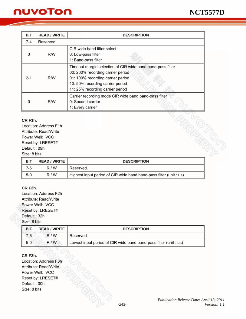
NCT5577D
Publication Release Date: April 13, 2011 -245- Version: 1.1
BIT READ / WRITE DESCRIPTION
7-4 Reserved.
3 R/W CIR wide band filter select 0: Low-pass filter 1: Band-pass filter
2-1 R/W
Timeout margin selection of CIR wide band band-pass filter 00: 200% recording carrier period 01: 100% recording carrier period 10: 50% recording carrier period 11: 25% recording carrier period
0 R/W Carrier recording mode CIR wide band band-pass filter 0: Second carrier 1: Every carrier
CR F1h. Location: Address F1h Attribute: Read/Write Power Well: VCC Reset by: LRESET# Default : 09h Size: 8 bits
BIT READ / WRITE DESCRIPTION
7-6 R / W Reserved.
5-0 R / W Highest input period of CIR wide band band-pass filter (unit : us)
CR F2h. Location: Address F2h Attribute: Read/Write Power Well: VCC Reset by: LRESET# Default : 32h Size: 8 bits
BIT READ / WRITE DESCRIPTION
7-6 R / W Reserved.
5-0 R / W Lowest input period of CIR wide band band-pass filter (unit : us)
CR F3h. Location: Address F3h Attribute: Read/Write Power Well: VCC Reset by: LRESET# Default : 00h Size: 8 bits

NCT5577D
Publication Release Date: April 13, 2011 -246- Version: 1.1
BIT READ / WRITE DESCRIPTION
7-6 R / W Reserved.
5-0 R / W Recording carrier period of CIR wide band band-pass filter (unit : us)

NCT5577D
Publication Release Date: April 13, 2011 -247- Version: 1.1
19.6 Logical Device 7 (GPIO7, GPIO8, GPIO9) CR 30h. Location: Address 30h Attribute: Read/Write Power Well: VSB Reset by: RSMRST# Default : 03h Size: 8 bits
BIT READ / WRITE DESCRIPTION
7-2 Reserved.
1 R / W 0: GPIO9 is inactive. 1: GPIO9 is active.
0 R / W 0: GPIO8 is inactive. 1: GPIO8 is active.
CR E0h. GPIO7 I/O Register Location: Address E0h Attribute: Read/Write Power Well: VSB Reset by: GP7X_MRST Default : FFh Size: 8 bits
BIT READ / WRITE DESCRIPTION
7~0 R / W GPIO7 I/O register 0: The respective GPIO7 PIN is programmed as an output port 1: The respective GPIO7 PIN is programmed as an input port.
CR E1h. GPIO7 Data Register Location: Address E1h Attribute: Read/Write Power Well: VSB Reset by: GP7X_MRST Default : 00h Size: 8 bits
BIT READ / WRITE DESCRIPTION
R / W GPIO7 Data register For output ports, the respective bits can be read/written and produced to pins. 7~0
Read Only For input ports, the respective bits can be read only from pins. Write accesses will be ignored.
CR E2h. GPIO7 Inversion Register Location: Address E2h Attribute: Read/Write Power Well: VSB

NCT5577D
Publication Release Date: April 13, 2011 -248- Version: 1.1
Reset by: GP7X_MRST Default : 00h Size: 8 bits
BIT READ / WRITE DESCRIPTION
7~0 R / W
GPIO7 Inversion register 0: The respective bit and the port value are the same. 1: The respective bit and the port value are inverted. (Both Input & Output ports)
CR E3h. GPIO7 Status Register Location: Address E3h Attribute: Read Only Power Well: VSB Reset by: GP7X_MRST Default : 00h Size: 8 bits
BIT READ / WRITE DESCRIPTION
7~0 Read Only Read-Clear
GPIO7 Event Status Bit 7-0 corresponds to GP77-GP70, respectively. 0 : No active edge (rising/falling) has been detected 1 : An active edge (rising/falling) has been detected Read the status bit clears it to 0.
CR E4h. GPIO8 I/O Register Location: Address E4h Attribute: Read/Write Power Well: VSB Reset by: GP8X_MRST Default : Efh Size: 8 bits
BIT READ / WRITE DESCRIPTION
7~0 R / W GPIO8 I/O register 0: The respective GPIO8 PIN is programmed as an output port 1: The respective GPIO8 PIN is programmed as an input port.
CR E5h. GPIO8 Data Register Location: Address E5h Attribute: Read/Write Power Well: VSB Reset by: GP8X_MRST Default : 00h Size: 8 bits
BIT READ / WRITE DESCRIPTION

NCT5577D
Publication Release Date: April 13, 2011 -249- Version: 1.1
BIT READ / WRITE DESCRIPTION
R / W GPIO8 Data register For output ports, the respective bits can be read/written and produced to pins. 7~0
Read Only For input ports, the respective bits can be read only from pins. Write accesses will be ignored.
CR E6h. GPIO8 Inversion Registe Location: Address E6h Attribute: Read/Write Power Well: VSB Reset by: GP8X_MRST Default : 00h Size: 8 bits
BIT READ / WRITE DESCRIPTION
7~0 R / W
GPIO8 Inversion register 0: The respective bit and the port value are the same. 1: The respective bit and the port value are inverted. (Both Input & Output ports)
CR E7h. GPIO8 Status Register Location: Address E7h Attribute: Read Only Power Well: VSB Reset by: GP8X_MRST Default : 00h Size: 8 bits
BIT READ / WRITE DESCRIPTION
7~0 Read Only Read-Clear
GPIO8 Event Status Bit 7-0 corresponds to GP87-GP80, respectively. 0 : No active edge (rising/falling) has been detected 1 : An active edge (rising/falling) has been detected Read the status bit clears it to 0.
CR E8h. GPIO9 I/O Register Location: Address E8h Attribute: Read/Write Power Well: VSB Reset by: GP9X_MRST Default : FFh Size: 8 bits
BIT READ / WRITE DESCRIPTION

NCT5577D
Publication Release Date: April 13, 2011 -250- Version: 1.1
BIT READ / WRITE DESCRIPTION
7~0 R / W GPIO9 I/O register 0: The respective GPIO9 PIN is programmed as an output port 1: The respective GPIO9 PIN is programmed as an input port.
CR E9h. GPIO9 Data Register Location: Address E9h Attribute: Read/Write Power Well: VSB Reset by: GP9X_MRST Default : 00h Size: 8 bits
BIT READ / WRITE DESCRIPTION
R / W GPIO9 Data register For output ports, the respective bits can be read/written and produced to pins. 7~0
Read Only For input ports, the respective bits can be read only from pins. Write accesses will be ignored.
CR EAh. GPIO9 Inversion Register Location: Address EAh Attribute: Read/Write Power Well: VSB Reset by: GP9X_MRST Default : 00h Size: 8 bits
BIT READ / WRITE DESCRIPTION
7~0 R / W
GPIO9 Inversion register 0: The respective bit and the port value are the same. 1: The respective bit and the port value are inverted. (Both Input & Output ports)
CR EBh. GPIO9 Status Register Location: Address EBh Attribute: Read Only Power Well: VSB Reset by: GP9X_MRST Default : 00h Size: 8 bits
BIT READ / WRITE DESCRIPTION
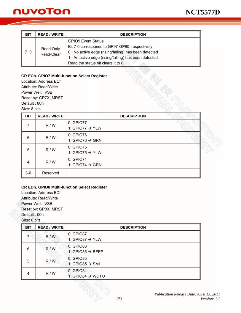
NCT5577D
Publication Release Date: April 13, 2011 -251- Version: 1.1
BIT READ / WRITE DESCRIPTION
7~0 Read Only Read-Clear
GPIO9 Event Status Bit 7-0 corresponds to GP97-GP90, respectively. 0 : No active edge (rising/falling) has been detected 1 : An active edge (rising/falling) has been detected Read the status bit clears it to 0.
CR ECh. GPIO7 Multi-function Select Register Location: Address ECh Attribute: Read/Write Power Well: VSB Reset by: GP7X_MRST Default : 00h Size: 8 bits
BIT READ / WRITE DESCRIPTION
7 R / W 0: GPIO77 1: GPIO77 YLW
6 R / W 0: GPIO76 1: GPIO76 GRN
5 R / W 0: GPIO75 1: GPIO75 YLW
4 R / W 0: GPIO74 1: GPIO74 GRN
3-0 Reserved
CR EDh. GPIO8 Multi-function Select Register Location: Address EDh Attribute: Read/Write Power Well: VSB Reset by: GP8X_MRST Default : 00h Size: 8 bits
BIT READ / WRITE DESCRIPTION
7 R / W 0: GPIO87 1: GPIO87 YLW
6 R / W 0: GPIO86 1: GPIO86 BEEP
5 R / W 0: GPIO85 1: GPIO85 SMI
4 R / W 0: GPIO84 1: GPIO84 WDTO
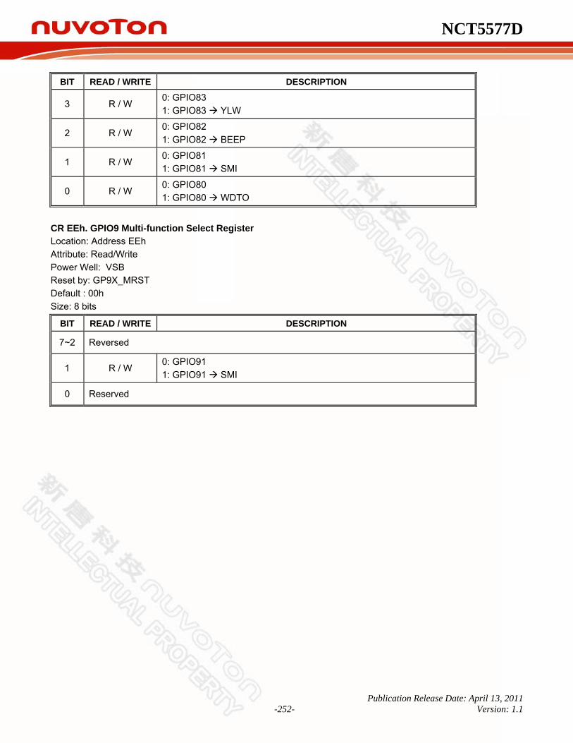
NCT5577D
Publication Release Date: April 13, 2011 -252- Version: 1.1
BIT READ / WRITE DESCRIPTION
3 R / W 0: GPIO83 1: GPIO83 YLW
2 R / W 0: GPIO82 1: GPIO82 BEEP
1 R / W 0: GPIO81 1: GPIO81 SMI
0 R / W 0: GPIO80 1: GPIO80 WDTO
CR EEh. GPIO9 Multi-function Select Register Location: Address EEh Attribute: Read/Write Power Well: VSB Reset by: GP9X_MRST Default : 00h Size: 8 bits
BIT READ / WRITE DESCRIPTION
7~2 Reversed
1 R / W 0: GPIO91 1: GPIO91 SMI
0 Reserved
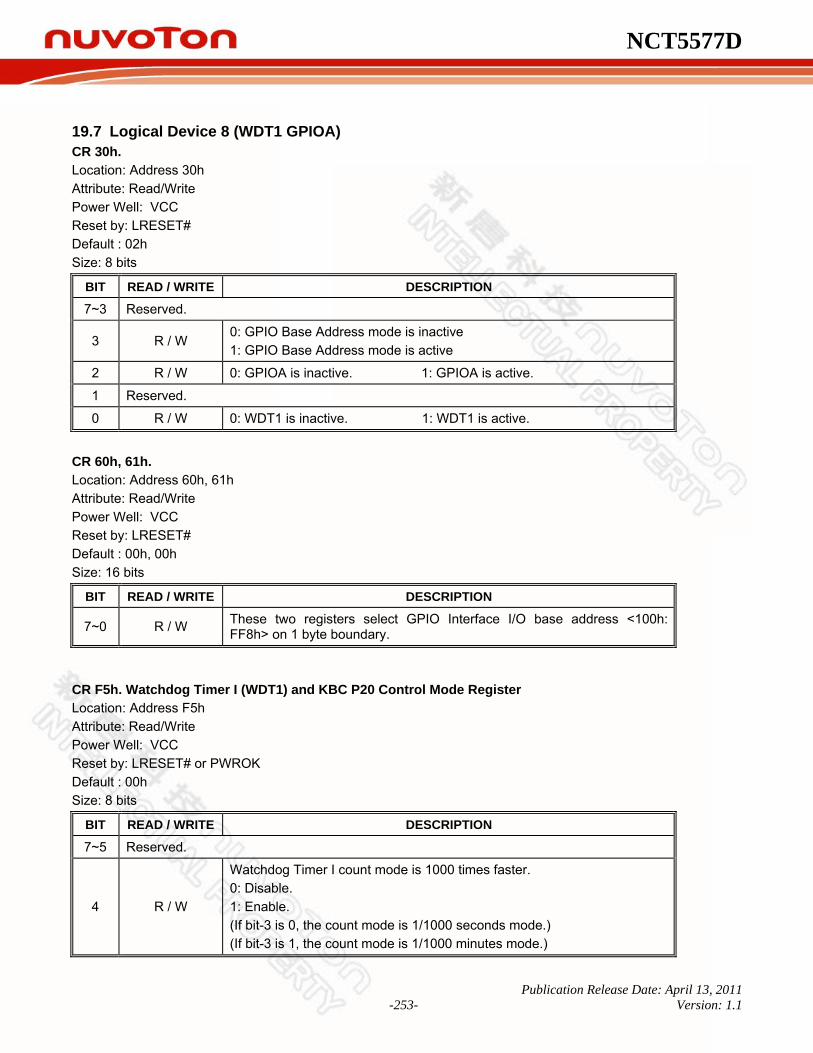
NCT5577D
Publication Release Date: April 13, 2011 -253- Version: 1.1
19.7 Logical Device 8 (WDT1 GPIOA) CR 30h. Location: Address 30h Attribute: Read/Write Power Well: VCC Reset by: LRESET# Default : 02h Size: 8 bits
BIT READ / WRITE DESCRIPTION
7~3 Reserved.
3 R / W 0: GPIO Base Address mode is inactive 1: GPIO Base Address mode is active
2 R / W 0: GPIOA is inactive. 1: GPIOA is active.
1 Reserved.
0 R / W 0: WDT1 is inactive. 1: WDT1 is active.
CR 60h, 61h. Location: Address 60h, 61h Attribute: Read/Write Power Well: VCC Reset by: LRESET# Default : 00h, 00h Size: 16 bits
BIT READ / WRITE DESCRIPTION
7~0 R / W These two registers select GPIO Interface I/O base address <100h: FF8h> on 1 byte boundary.
CR F5h. Watchdog Timer I (WDT1) and KBC P20 Control Mode Register Location: Address F5h Attribute: Read/Write Power Well: VCC Reset by: LRESET# or PWROK Default : 00h Size: 8 bits
BIT READ / WRITE DESCRIPTION
7~5 Reserved.
4 R / W
Watchdog Timer I count mode is 1000 times faster. 0: Disable. 1: Enable. (If bit-3 is 0, the count mode is 1/1000 seconds mode.) (If bit-3 is 1, the count mode is 1/1000 minutes mode.)

NCT5577D
Publication Release Date: April 13, 2011 -254- Version: 1.1
BIT READ / WRITE DESCRIPTION
3 R / W Select Watchdog Timer I count mode. 0: Second Mode. 1: Minute Mode.
2 R / W Enable the rising edge of a KBC reset (P20) to issue a time-out event. 0: Disable. 1: Enable.
1 R / W
Disable / Enable the Watchdog Timer I output low pulse to the KBRST# pin (PIN12) 0: Disable. 1: Enable.
0 Reversed
CR F6h. Watchdog Timer I (WDT1) Counter Register Location: Address F6h Attribute: Read/Write Power Well: VCC Reset by: LRESET# or PWROK Default : 00h Size: 8 bits
BIT READ / WRITE DESCRIPTION
7~0 R / W
Watch Dog Timer I Time-out value. Writing a non-zero value to this register causes the counter to load the value into the Watch Dog Counter and start counting down. If CR F7h, bits 7 and 6 are set, any Mouse Interrupt or Keyboard Interrupt event causes the previously-loaded, non-zero value to be reloaded to the Watch Dog Counter and the count down resumes. Reading this register returns the current value in the Watch Dog Counter, not the Watch Dog Timer Time-out value. 00h: Time-out Disable 01h: Time-out occurs after 5.03x10⁷ CLKIN cycle time, by analogy.
(5.03x107x (1/48MHz) = 1.046s)
CR F7h. Watchdog Timer I (WDT1) Control & Status Register Location: Address F7h Attribute: Read/Write Power Well: VCC Reset by: LRESET# or PWROK Default : 00h Size: 8 bits
BIT READ / WRITE DESCRIPTION
7 R / W Mouse interrupt reset enables watch-dog timer reload 0: Watchdog Timer I is not affected by mouse interrupt. 1: Watchdog Timer I is reset by mouse interrupt.
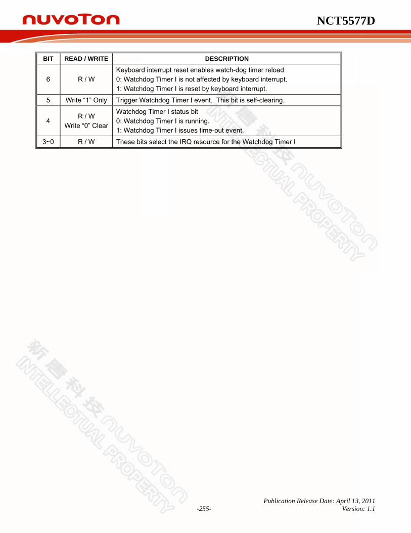
NCT5577D
Publication Release Date: April 13, 2011 -255- Version: 1.1
BIT READ / WRITE DESCRIPTION
6 R / W Keyboard interrupt reset enables watch-dog timer reload 0: Watchdog Timer I is not affected by keyboard interrupt. 1: Watchdog Timer I is reset by keyboard interrupt.
5 Write “1” Only Trigger Watchdog Timer I event. This bit is self-clearing.
4 R / W
Write “0” Clear
Watchdog Timer I status bit 0: Watchdog Timer I is running. 1: Watchdog Timer I issues time-out event.
3~0 R / W These bits select the IRQ resource for the Watchdog Timer I

NCT5577D
Publication Release Date: April 13, 2011 -256- Version: 1.1
19.8 Logical Device 9 (GPIO2, GPIO3, GPIO4, GPIO5, GPIO7) CR 30h. Location: Address 30h Attribute: Read/Write Power Well: VSB Reset by: RSMRST# Default : 04h Size: 8 bits
BIT READ / WRITE DESCRIPTION
7 R / W 0: GPIO7 is inactive. 1: GPIO7 is active.
6 Reserved.
5 R / W 0: GPIO5 is inactive. 1: GPIO5 is active.
4 R / W 0: GPIO4 is inactive. 1: GPIO4 is active.
3 R / W 0: GPIO3 is inactive. 1: GPIO3 is active
2 R / W 0: GPIO2 is inactive. 1: GPIO2 is active.
1~0 Reserved.
CR E0h. GPIO2 I/O Register Location: Address E0h Attribute: Read/Write Power Well: VSB Reset by: GP2X_MRST Default : DFh Size: 8 bits
BIT READ / WRITE DESCRIPTION
7~0 R / W GPIO2 I/O register 0: The respective GPIO2 PIN is programmed as an output port 1: The respective GPIO2 PIN is programmed as an input port.
CR E1h. GPIO2 Data Register Location: Address E1h Attribute: Read/Write Power Well: VSB Reset by: GP2X_MRST Default : 00h Size: 8 bits
BIT READ / WRITE DESCRIPTION
R / W GPIO2 Data register For output ports, the respective bits can be read and written by the pins.
7~0 Read Only For Input ports, the respective bits can only be read by the pins. Write
accesses are ignored.
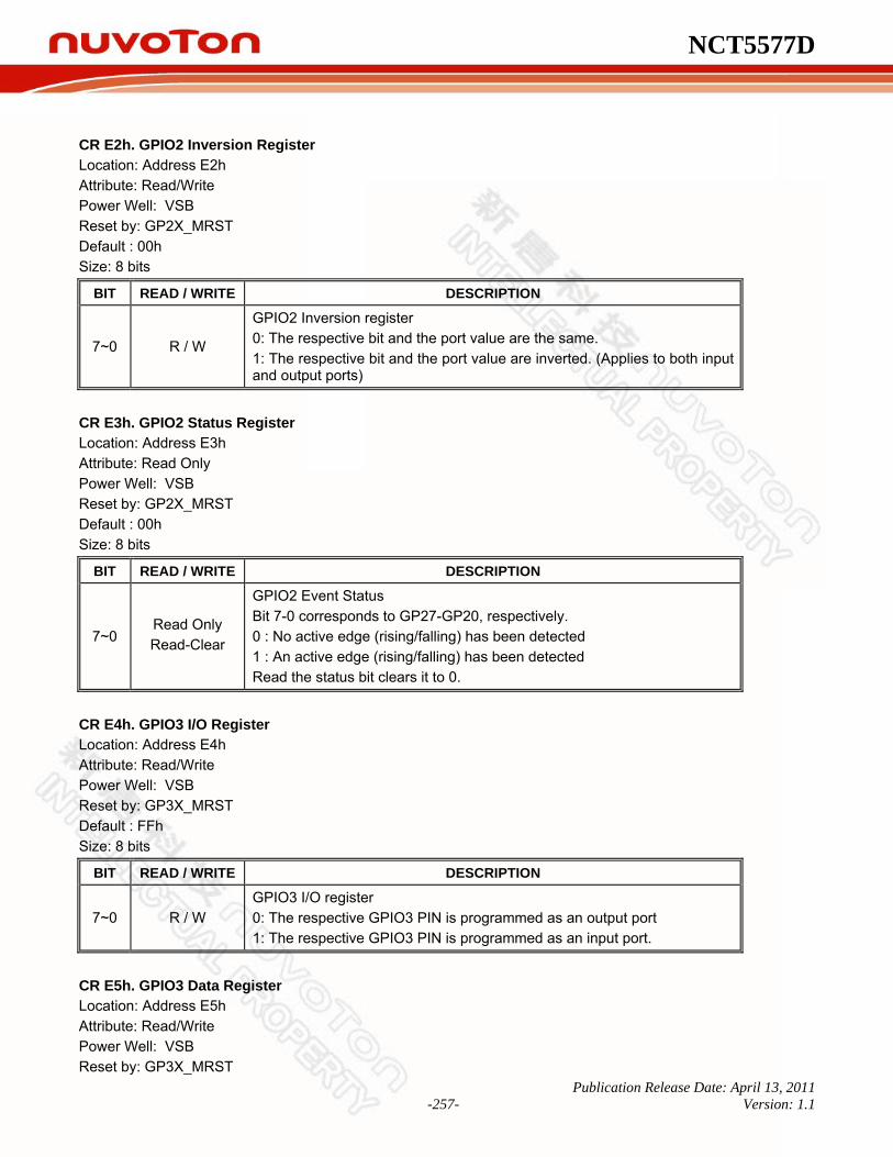
NCT5577D
Publication Release Date: April 13, 2011 -257- Version: 1.1
CR E2h. GPIO2 Inversion Register Location: Address E2h Attribute: Read/Write Power Well: VSB Reset by: GP2X_MRST Default : 00h Size: 8 bits
BIT READ / WRITE DESCRIPTION
7~0 R / W
GPIO2 Inversion register 0: The respective bit and the port value are the same. 1: The respective bit and the port value are inverted. (Applies to both input and output ports)
CR E3h. GPIO2 Status Register Location: Address E3h Attribute: Read Only Power Well: VSB Reset by: GP2X_MRST Default : 00h Size: 8 bits
BIT READ / WRITE DESCRIPTION
7~0 Read Only Read-Clear
GPIO2 Event Status Bit 7-0 corresponds to GP27-GP20, respectively. 0 : No active edge (rising/falling) has been detected 1 : An active edge (rising/falling) has been detected Read the status bit clears it to 0.
CR E4h. GPIO3 I/O Register Location: Address E4h Attribute: Read/Write Power Well: VSB Reset by: GP3X_MRST Default : FFh Size: 8 bits
BIT READ / WRITE DESCRIPTION
7~0 R / W GPIO3 I/O register 0: The respective GPIO3 PIN is programmed as an output port 1: The respective GPIO3 PIN is programmed as an input port.
CR E5h. GPIO3 Data Register Location: Address E5h Attribute: Read/Write Power Well: VSB Reset by: GP3X_MRST

NCT5577D
Publication Release Date: April 13, 2011 -258- Version: 1.1
Default : 00h Size: 8 bits
BIT READ / WRITE DESCRIPTION
R / W GPIO3 Data register For output ports, the respective bits can be read and written by the pins.
7~0 Read Only For Input ports, the respective bits can only be read by the pins. Write
accesses are ignored.
CR E6h. GPIO3 Inversion Register Location: Address E6h Attribute: Read/Write Power Well: VSB Reset by: GP3X_MRST Default : 00h Size: 8 bits
BIT READ / WRITE DESCRIPTION
7~0 R / W
GPIO3 Inversion register 0: The respective bit and the port value are the same. 1: The respective bit and the port value are inverted. (Applies to both input and output ports)
CR E7h. GPIO3 Status Register Location: Address E7h Attribute: Read Only Power Well: VSB Reset by: GP3X_MRST Default : 00h Size: 8 bits
BIT READ / WRITE DESCRIPTION
7~0 Read Only Read-Clear
GPIO3 Event Status Bit 7-0 corresponds to GP37-GP30, respectively. 0 : No active edge(rising/falling) has been detected 1 : An active edge(rising/falling) has been detected Read the status bit clears it to 0.
CR E9h. GPIO2 Multi-function Select Register Location: Address E9h Attribute: Read/Write Power Well: VSB Reset by: GP2X_MRST Default : 00h Size: 8 bits
BIT READ / WRITE DESCRIPTION

NCT5577D
Publication Release Date: April 13, 2011 -259- Version: 1.1
BIT READ / WRITE DESCRIPTION
7-6 Reserved
5 R / W 0: GPIO25 1: GPIO25 SMI
4 R / W 0: GPIO24 1: GPIO24 WDTO
3 R / W 0: GPIO23 1: GPIO23 GRN
2 R / W 0: GPIO22 1: GPIO22 BEEP
1 R / W 0: GPIO21 1: GPIO21 SMI
0 R / W 0: GPIO20 1: GPIO20 WDTO
CR EAh. GPIO3 Multi-function Select Register Location: Address EAh Attribute: Read/Write Power Well: VSB Reset by: GP3X_MRST Default : 00h Size: 8 bits
BIT READ / WRITE DESCRIPTION
7 Reserved
6 R / W 0: GPIO36 1: GPIO36 BEEP
5 R / W 0: GPIO35 1: GPIO35 SMI
4 R / W 0: GPIO34 1: GPIO34 WDTO
3 R / W 0: GPIO33 1: GPIO33 GRN
2 R / W 0: GPIO32 1: GPIO32 BEEP
1 Reserved
0 R / W 0: GPIO30 1: GPIO30 WDTO
CR EBh. GPIO5 Multi-function Select Register Location: Address EBh Attribute: Read/Write

NCT5577D
Publication Release Date: April 13, 2011 -260- Version: 1.1
Power Well: VSB Reset by: GP5X_MRST Default : 00h Size: 8 bits
BIT READ / WRITE DESCRIPTION
7-5 Reserved
4 R / W 0: GPIO54 1: GPIO54 WDTO
3 R / W 0: GPIO53 1: GPIO53 GRN
2 R / W 0: GPIO52 1: GPIO52 BEEP
1 R / W 0: GPIO51 1: GPIO51 SMI
0 Reserved
CR F0h. GPIO4 I/O Register Location: Address F0h Attribute: Read/Write Power Well: VSB Reset by: GP4X_MRST Default : FFh Size: 8 bits
BIT READ / WRITE DESCRIPTION
7~0 R / W GPIO4 I/O register 0: The respective GPIO4 PIN is programmed as an output port 1: The respective GPIO4 PIN is programmed as an input port.
CR F1h. GPIO4 Data Register Location: Address F1h Attribute: Read/Write Power Well: VSB Reset by: GP4X_MRST Default : 00h Size: 8 bits
BIT READ / WRITE DESCRIPTION
R / W GPIO4 Data register For output ports, the respective bits can be read and written by the pins.
7~0 Read Only For Input ports, the respective bits can only be read by the pins. Write
accesses are ignored.
CR F2h. GPIO4 Inversion Register

NCT5577D
Publication Release Date: April 13, 2011 -261- Version: 1.1
Location: Address F2h Attribute: Read/Write Power Well: VSB Reset by: GP4X_MRST Default : 00h Size: 8 bits
BIT READ / WRITE DESCRIPTION
7~0 R / W
GPIO4 Inversion register 0: The respective bit and the port value are the same. 1: The respective bit and the port value are inverted. (Applies to both input and output ports)
CR E8h. GPIO4 Status Register Location: Address E8h Attribute: Read Only Power Well: VSB Reset by: GP4X_MRST Default : 00h Size: 8 bits
BIT READ / WRITE DESCRIPTION
7~0 Read Only Read-Clear
GPIO4 Event Status Bit 7-0 corresponds to GP47-GP40, respectively. 0 : No active edge (rising/falling) has been detected 1 : An active edge (rising/falling) has been detected Read the status bit clears it to 0.
CR EEh. GPIO4 Multi-function Select Register Location: Address EEh Attribute: Read/Write Power Well: VSB Reset by: GP4X_MRST Default : 00h Size: 8 bits
BIT READ / WRITE DESCRIPTION
7 R / W 0: GPIO47 1: GPIO47 YLW
6 R / W 0: GPIO46 1: GPIO46 BEEP
5 R / W 0: GPIO45 1: GPIO45 SMI
4 R / W 0: GPIO44 1: GPIO44 WDTO
3 R / W 0: GPIO43 1: GPIO43 YLW

NCT5577D
Publication Release Date: April 13, 2011 -262- Version: 1.1
BIT READ / WRITE DESCRIPTION
2 R / W 0: GPIO42 1: GPIO42 BEEP
1 R / W 0: GPIO41 1: GPIO41 SMI
0 R / W 0: GPIO40 1: GPIO40 WDTO
CR F4h. GPIO5 I/O Register Location: Address F4h Attribute: Read/Write Power Well: VSB Reset by: GP5X_MRST Default : FFh Size: 8 bits
BIT READ / WRITE DESCRIPTION
7~5 Reserved.
4~0 R / W GPIO5 I/O register 0: The respective GPIO5 PIN is programmed as an output port 1: The respective GPIO5 PIN is programmed as an input port.
CR F5h. GPIO5 Data Register Location: Address F5h Attribute: Read/Write Power Well: VSB Reset by: GP5X_MRST Default : 00h Size: 8 bits
BIT READ / WRITE DESCRIPTION
7~5 Reserved.
R / W GPIO5 Data register For output ports, the respective bits can be read and written by the pins.
4~0 Read Only For input ports, the respective bits can only be read by the pins. Write
accesses are ignored.
CR F6h. GPIO5 Inversion Register Location: Address F6h Attribute: Read/Write Power Well: VSB Reset by: GP5X_MRST Default : 00h Size: 8 bits

NCT5577D
Publication Release Date: April 13, 2011 -263- Version: 1.1
BIT READ / WRITE DESCRIPTION
7~5 Reserved.
4~0 R / W
GPIO5 Inversion register 0: The respective bit and the port value are the same. 1: The respective bit and the port value are inverted. (Applies to both input and output ports)
CR F7h. GPIO5 Status Register Location: Address F7h Attribute: Read Only Power Well: VSB Reset by: GP5X_MRST Default : 00h Size: 8 bits
BIT READ / WRITE DESCRIPTION
7~5 Reserved.
4~0 Read Only Read-Clear
GPIO5 Event Status Bit 7-0 corresponds to GP57-GP50, respectively. 0 : No active edge (rising/falling) has been detected 1 : An active edge (rising/falling) has been detected Read the status bit clears it to 0.
CR FEh. Input Detected Type Register Location: Address FEh Attribute: Read/Write Power Well: VSB Reset by: GP4X_MRST or GP9X_MRST Default : 00h Size: 8 bits
BIT READ / WRITE DESCRIPTION
7~5 Reserved.
4 R / W 0: Enable GP41 input de-bouncer 1: Disable GP41 input de-bouncer
3~1 Reserved.
0 R / W 0: GP41 trigger type: edge 1: GP41 trigger type: level

NCT5577D
Publication Release Date: April 13, 2011 -264- Version: 1.1
19.9 Logical Device A (ACPI) CR E0h. Location: Address E0h Attribute: Read/Write Power Well: VRTC Reset by: Battery reset Default : 01h Size: 8 bits
BIT READ / WRITE DESCRIPTION
7 R / W
DIS_PSIN => Disable the panel switch input to turn on the system power supply. 0: PSIN is wire-AND and connected to PSOUT#. 1: PSIN is blocked and cannot affect PSOUT#.
6 R / W Enable KBC wake-up 0: Disable keyboard wake-up function via PSOUT#. 1: Enable keyboard wake-up function via PSOUT#.
5 R / W Enable Mouse wake-up 0: Disable mouse wake-up function via PSOUT#. 1: Enable mouse wake-up function via PSOUT#.
4 R / W
MSRKEY => Three keys (ENMDAT_UP, CRE6[7]; MSRKEY, CRE0[4]; MSXKEY, CRE0[1]) define the combinations of the mouse wake-up events. Please see the following table for the details. ENMDAT_UP MSRKEY MSXKEY Wake-up event
1 x 1 Any button clicked or any movement.
1 x 0 One click of left or right button.
0 0 1 One click of the left button. 0 1 1 One click of the right button. 0 0 0 Two clicks of the left button. 0 1 0 Two clicks of the right button.
3 R / W Enable CIR wake-up 0: Disable CIR wake-up function via PSOUT#. 1: Enable CIR wake-up function via PSOUT#.
2 R / W Keyboard / Mouse swap enable 0: Normal mode. 1: Keyboard / Mouse ports are swapped.
1 R / W
MSXKEY => Three keys (ENMDAT_UP, CRE6[7]; MSRKEY, CRE0[4]; MSXKEY, CRE0[1]) define the combinations of the mouse wake-up events. Please check out the table in CRE0[4] for the detailed.
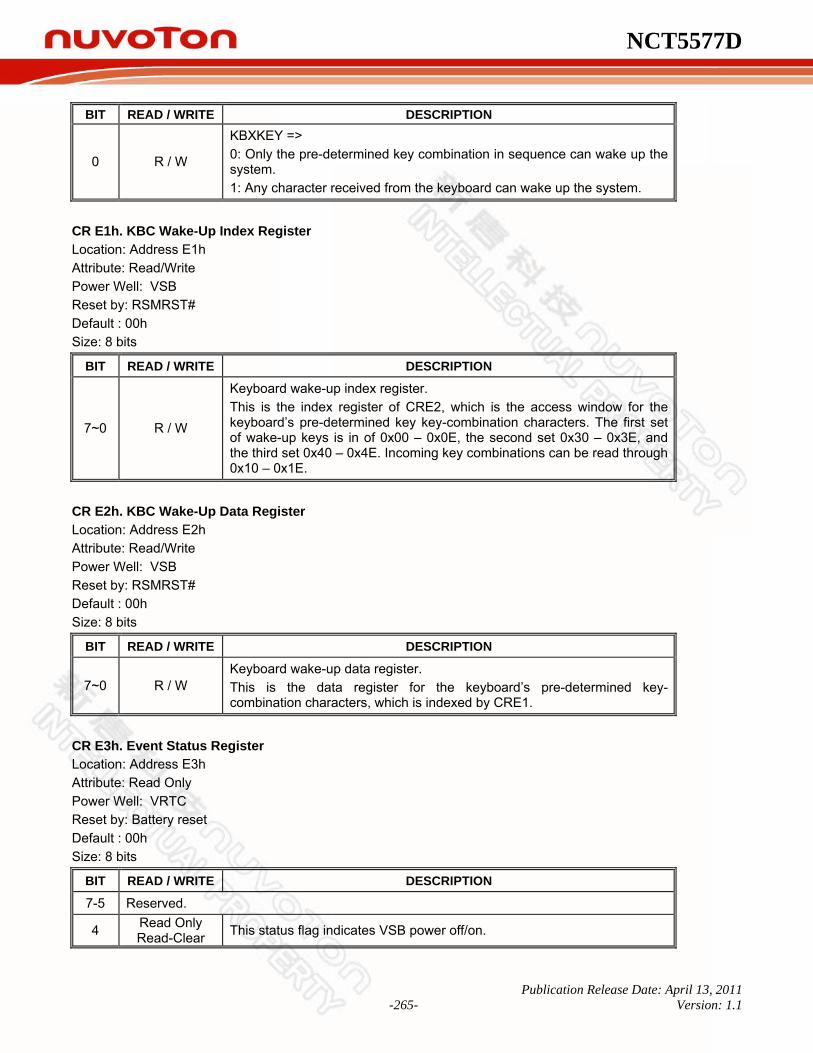
NCT5577D
Publication Release Date: April 13, 2011 -265- Version: 1.1
BIT READ / WRITE DESCRIPTION
0 R / W
KBXKEY => 0: Only the pre-determined key combination in sequence can wake up the system. 1: Any character received from the keyboard can wake up the system.
CR E1h. KBC Wake-Up Index Register Location: Address E1h Attribute: Read/Write Power Well: VSB Reset by: RSMRST# Default : 00h Size: 8 bits
BIT READ / WRITE DESCRIPTION
7~0 R / W
Keyboard wake-up index register. This is the index register of CRE2, which is the access window for the keyboard’s pre-determined key key-combination characters. The first set of wake-up keys is in of 0x00 – 0x0E, the second set 0x30 – 0x3E, and the third set 0x40 – 0x4E. Incoming key combinations can be read through 0x10 – 0x1E.
CR E2h. KBC Wake-Up Data Register Location: Address E2h Attribute: Read/Write Power Well: VSB Reset by: RSMRST# Default : 00h Size: 8 bits
BIT READ / WRITE DESCRIPTION
7~0 R / W Keyboard wake-up data register. This is the data register for the keyboard’s pre-determined key-combination characters, which is indexed by CRE1.
CR E3h. Event Status Register Location: Address E3h Attribute: Read Only Power Well: VRTC Reset by: Battery reset Default : 00h Size: 8 bits
BIT READ / WRITE DESCRIPTION
7-5 Reserved.
4 Read Only Read-Clear This status flag indicates VSB power off/on.

NCT5577D
Publication Release Date: April 13, 2011 -266- Version: 1.1
BIT READ / WRITE DESCRIPTION
3 Read Only Read-Clear
Thermal shutdown status. 0: No thermal shutdown event issued. 1: Thermal shutdown event issued.
2 Read Only Read-Clear
PSIN_STS 0: No PSIN event issued. 1: PSIN event issued.
1 Read Only Read-Clear
MSWAKEUP_STS => The bit is latched by the mouse wake-up event. 0: No mouse wake-up event issued. 1: Mouse wake-up event issued.
0 Read Only Read-Clear
KBWAKEUP_STS => The bit is latched by the keyboard wake-up event. 0: No keyboard wake-up event issued. 1: Keyboard wake-up event issued.
CR E4h. Location: Address E4h Attribute: Read/Write Power Well: VRTC Reset by: Battery reset, PWROK(Bit4), LRESET#(Bit3-2) Default : 00h Size: 8 bits
BIT READ / WRITE DESCRIPTION 7 Reserved
6~5 R / W
Power-loss control bits => (VBAT) Bits 6 5 0 0: System always turns off when it returns from power-loss state. 0 1: System always turns on when it returns from power-loss state. 1 0: System turns off / on when it returns from power-loss state depending
on the state before the power loss. 1 1: User defines the resuming state before power loss.(refer to Logic
Device A, CRE6[4])
4 R / W VSBGATE# Enable bit => 0: Disable. 1: Enable.
3 R / W Keyboard wake-up options. 0: Password or sequence hot keys programmed in the registers. 1: Any key.
2 R / W
Enable the hunting mode for all wake-up events set in CRE0. This bit is cleared when any wake-up events is captured. (this bit is reset by LRESET#) (Note. This bit is to generate PSOUT# via KB or MS under S1.) 0: Disable. 1: Enable.
1~0 Reserved. CR E5h. GPIOs Reset Source Register

NCT5577D
Publication Release Date: April 13, 2011 -267- Version: 1.1
Location: Address E5h Attribute: Read/Write Power Well: VSB Reset by: RSMRST# Default : 02h Size: 8 bits
BIT READ / WRITE DESCRIPTION
7 R / W GPAX_MRST 0: GPAX reset by LRESET#. 1: GPAX reset by PWROK.
6 R / W GP9X_MRST 0: GP9X reset by RSMRST#. 1: GP9X reset by SLPS5.
5 R / W GP8X_MRST 0: GP8X reset by RSMRST#. 1: GP8X reset by SLPS5.
4 R / W GP7X_MRST 0: GP7X reset by RSMRST#. 1: GP7X reset by SLPS5.
3~2 Reserved.
1 R / W PWROK source selection. 0: PSON#. 1: SLP_S3#.
0 R / W ATXPGD signal to control PWROK 0: Enable. 1: Disable.
CR E6h. Location: Address E6h Attribute: Read/Write Power Well: VRTC Reset by: RSMRST#(Bit7, Bit5, Bit3-1), Battery reset(Bit6, Bit4), PWROK(Bit0) Default : 1Ch Size: 8 bits
BIT READ / WRITE DESCRIPTION
7 R / W
ENMDAT => Three keys (ENMDAT_UP, CRE6[7]; MSRKEY, CRE0[4]; MSXKEY, CRE0[1]) define the combinations of the mouse wake-up events. Please see the table in CRE0, bit 4 for the details.
6~5 Reserved.
4 R / W Power-loss Last State Flag. 0: ON 1: OFF.

NCT5577D
Publication Release Date: April 13, 2011 -268- Version: 1.1
BIT READ / WRITE DESCRIPTION
3~1 R / W
PWROK_DEL Set the delay time when rising from 3VCC to PWROK Bits 3 2 1 0 0 0: 300 ~ 600mS 0 0 1: 330 ~ 670mS 0 1 0: 390 ~ 730mS 0 1 1: 520 ~ 860mS 1 0 0: 200 ~ 300mS 1 0 1: 230 ~ 370mS 1 1 0: 290 ~ 430mS 1 1 1: 420 ~ 560mS
0 R / W PWROK_TRIG => 0: PWROK work normally. (Default) 1: Write 1 will let PWROK keep low or from high to low immediately.
CR E7h. Location: Address E7h Attribute: Read/Write Power Well: VRTC Reset by: RSMRST#(Bit7-5, Bit3-2), Battery reset(Bit4, Bit1-0) Default : 00h Size: 8 bits
BIT READ / WRITE DESCRIPTION
7 R / W
ENKD3 => Enable the third set of keyboard wake-up key combination. Its values are accessed through keyboard wake-up index register (CRE1) and keyboard wake-up data register (CRE2) at the index from 40h to 4eh. 0: Disable the third set of the key combinations. 1: Enable the third set of the key combinations.
6 R / W
ENKD2 => Enable the second set of keyboard wake-up key combination. Its values are accessed through keyboard wake-up index register (CRE1) and keyboard wake-up data register (CRE2) at the index from 30h to 3eh. 0: Disable the second set of the key combinations. 1: Enable the second set of the key combinations.
5 R / W
ENWIN98KEY => Enable Win98 keyboard dedicated key to wake-up system via PSOUT# when keyboard wake-up function is enabled. 0: Disable Win98 keyboard wake-up. 1: Enable Win98 keyboard wake-up.

NCT5577D
Publication Release Date: April 13, 2011 -269- Version: 1.1
BIT READ / WRITE DESCRIPTION
4 R / W
EN_ONPSOUT Disable/Enable to issue a 0.5s delay PSOUT# level when system returns from power loss state and is supposed to be on as described in CRE4[6:5], logic device A. (for SiS & VIA chipsets) 0: Disable. 1: Enable.
3 R / W Select WDT1 reset source 0: Watchdog timer is reset by LRESET#. 1: Watchdog timer is reset by PWROK.
2~1 Reserved.
0 R / W Hardware Monitor RESET source select 0: PWROK. 1: LRESET#.
CR E9h. GPIOs Reset Source Register Location: Address E9h Attribute: Read/Write Power Well: VSB Reset by: RSMRST# Default : 00h Size: 8 bits
BIT READ / WRITE DESCRIPTION
7-6 Reserved.
5 R / W GP5X_MRST 0: GP5X reset by RSMRST#. 1: GP5X reset by SLPS5.
4 R / W GP4X_MRST 0: GP4X reset by RSMRST#. 1: GP4X reset by SLPS5.
3 R / W GP3X_MRST 0: GP3X reset by RSMRST#. 1: GP3X reset by SLPS5.
2 R / W GP2X_MRST 0: GP2X reset by RSMRST#. 1: GP2X reset by SLPS5.
1-0 Reserved.
CR EEh. Location: Address EEh Attribute: Read/Write Power Well: VRTC Reset by: Battery reset Default : 01h
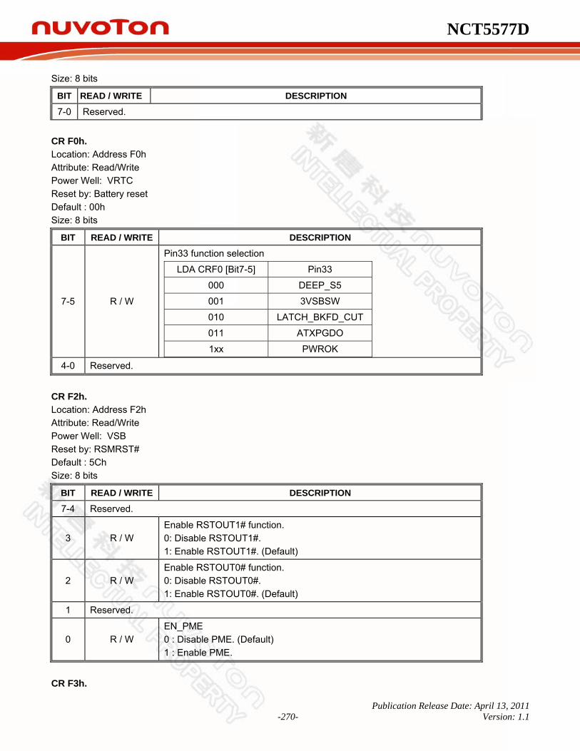
NCT5577D
Publication Release Date: April 13, 2011 -270- Version: 1.1
Size: 8 bits
BIT READ / WRITE DESCRIPTION
7-0 Reserved.
CR F0h. Location: Address F0h Attribute: Read/Write Power Well: VRTC Reset by: Battery reset Default : 00h Size: 8 bits
BIT READ / WRITE DESCRIPTION
7-5 R / W
Pin33 function selection
LDA CRF0 [Bit7-5] Pin33
000 DEEP_S5
001 3VSBSW
010 LATCH_BKFD_CUT
011 ATXPGDO
1xx PWROK 4-0 Reserved.
CR F2h. Location: Address F2h Attribute: Read/Write Power Well: VSB Reset by: RSMRST# Default : 5Ch Size: 8 bits
BIT READ / WRITE DESCRIPTION
7-4 Reserved.
3 R / W Enable RSTOUT1# function. 0: Disable RSTOUT1#. 1: Enable RSTOUT1#. (Default)
2 R / W Enable RSTOUT0# function. 0: Disable RSTOUT0#. 1: Enable RSTOUT0#. (Default)
1 Reserved.
0 R / W EN_PME 0 : Disable PME. (Default) 1 : Enable PME.
CR F3h.

NCT5577D
Publication Release Date: April 13, 2011 -271- Version: 1.1
Location: Address F3h Attribute: Read/Write Power Well: VSB Reset by: RSMRST# Default : 00h Size: 8 bits
BIT READ / WRITE DESCRIPTION
7~6 Reserved.
5 R / W-Clear PME status of the Mouse IRQ event. Write 1 to clear this status.
4 R / W-Clear PME status of the KBC IRQ event. Write 1 to clear this status.
3~2 Reserved.
1 R / W-Clear PME status of the URA IRQ event. Write 1 to clear this status.
0 Reserved.
CR F4h. Location: Address F4h Attribute: Read/Write Power Well: VSB Reset by: RSMRST# Default : 00h Size: 8 bits
BIT READ / WRITE DESCRIPTION
7~4 Reserved.
3 R / W-Clear PME status of the HM IRQ event. Write 1 to clear this status.
2 R / W-Clear PME status of the WDT1 event. Write 1 to clear this status.
1 Reserved.
0 R / W-Clear PME status of the RIB event. Write 1 to clear this status.
CR F6h. Location: Address F6h Attribute: Read/Write Power Well: VSB Reset by: LRESET#(Bit7), RSMRST# Default : 00h Size: 8 bits
BIT READ / WRITE DESCRIPTION

NCT5577D
Publication Release Date: April 13, 2011 -272- Version: 1.1
BIT READ / WRITE DESCRIPTION
7 R / W 0: Disable KB, MS interrupt of the KBC password event. 1: Enable KB, MS interrupt of the KBC password event.
6 Reserved.
5 R / W 0: Disable PME interrupt of the Mouse IRQ event. 1: Enable PME interrupt of the Mouse IRQ event.
4 R / W 0: Disable PME interrupt of the KBC IRQ event. 1: Enable PME interrupt of the KBC IRQ event.
3~2 Reserved.
1 R / W 0: Disable PME interrupt of the URA IRQ event. 1: Enable PME interrupt of the URA IRQ event.
0 Reserved.
CR F7h. Location: Address F7h Attribute: Read/Write Power Well: VSB Reset by: RSMRST# Default : C0h Size: 8 bits
BIT READ / WRITE DESCRIPTION
7 Reserved.
6 R / W RSTOUT1# Push-Pull/OD select 0: Open Drain 1: Push-Pull
5 Reserved
4 R / W 0: Disable PME interrupt of the CIRWAKEUP IRQ event. 1: Enable PME interrupt of the CIRWAKEUP IRQ event.
3 R / W 0: Disable PME interrupt of the HM IRQ event. 1: Enable PME interrupt of the HM IRQ event.
2 R / W 0: Disable PME interrupt of the WDT1 event. 1: Enable PME interrupt of the WDT1 event.
1 Reserved.
0 R / W 0: Disable PME interrupt of the RIB event. 1: Enable PME interrupt of the RIB event.
CR FEh. GPIO41 Event Route Selection Register Location: Address FEh Attribute: Read/Write Power Well: VSB Reset by: RSMRST# Default : 00h
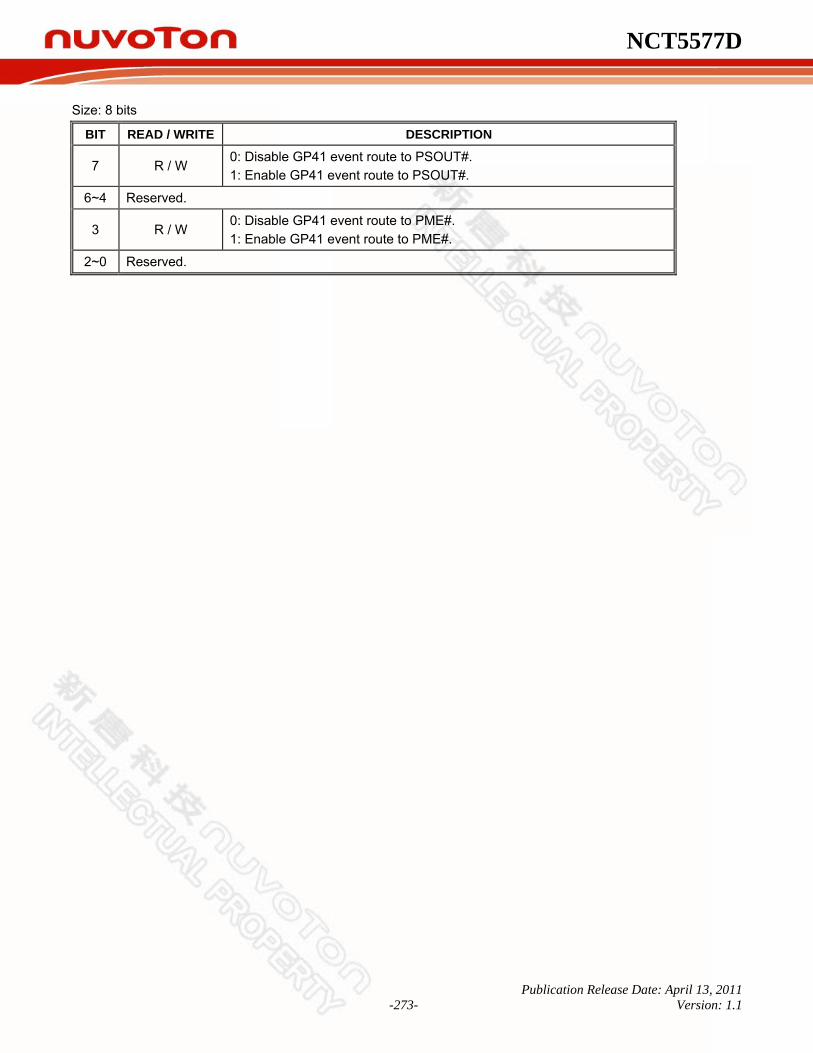
NCT5577D
Publication Release Date: April 13, 2011 -273- Version: 1.1
Size: 8 bits
BIT READ / WRITE DESCRIPTION
7 R / W 0: Disable GP41 event route to PSOUT#. 1: Enable GP41 event route to PSOUT#.
6~4 Reserved.
3 R / W 0: Disable GP41 event route to PME#. 1: Enable GP41 event route to PME#.
2~0 Reserved.
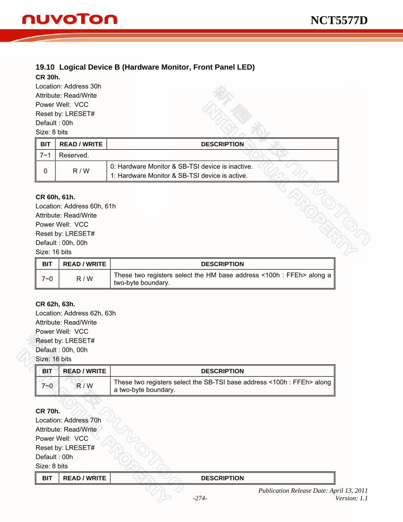
NCT5577D
Publication Release Date: April 13, 2011 -274- Version: 1.1
19.10 Logical Device B (Hardware Monitor, Front Panel LED) CR 30h. Location: Address 30h Attribute: Read/Write Power Well: VCC Reset by: LRESET# Default : 00h Size: 8 bits
BIT READ / WRITE DESCRIPTION
7~1 Reserved.
0 R / W 0: Hardware Monitor & SB-TSI device is inactive. 1: Hardware Monitor & SB-TSI device is active.
CR 60h, 61h. Location: Address 60h, 61h Attribute: Read/Write Power Well: VCC Reset by: LRESET# Default : 00h, 00h Size: 16 bits
BIT READ / WRITE DESCRIPTION
7~0 R / W These two registers select the HM base address <100h : FFEh> along a two-byte boundary.
CR 62h, 63h. Location: Address 62h, 63h Attribute: Read/Write Power Well: VCC Reset by: LRESET# Default : 00h, 00h Size: 16 bits
BIT READ / WRITE DESCRIPTION
7~0 R / W These two registers select the SB-TSI base address <100h : FFEh> along a two-byte boundary.
CR 70h. Location: Address 70h Attribute: Read/Write Power Well: VCC Reset by: LRESET# Default : 00h Size: 8 bits
BIT READ / WRITE DESCRIPTION
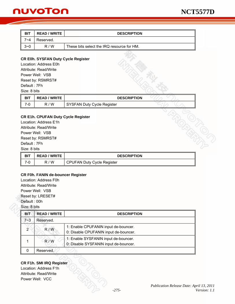
NCT5577D
Publication Release Date: April 13, 2011 -275- Version: 1.1
BIT READ / WRITE DESCRIPTION
7~4 Reserved.
3~0 R / W These bits select the IRQ resource for HM.
CR E0h. SYSFAN Duty Cycle Register Location: Address E0h Attribute: Read/Write Power Well: VSB Reset by: RSMRST# Default : 7Fh Size: 8 bits
BIT READ / WRITE DESCRIPTION
7-0 R / W SYSFAN Duty Cycle Register
CR E1h. CPUFAN Duty Cycle Register Location: Address E1h Attribute: Read/Write Power Well: VSB Reset by: RSMRST# Default : 7Fh Size: 8 bits
BIT READ / WRITE DESCRIPTION
7-0 R / W CPUFAN Duty Cycle Register
CR F0h. FANIN de-bouncer Register Location: Address F0h Attribute: Read/Write Power Well: VSB Reset by: LRESET# Default : 00h Size: 8 bits
BIT READ / WRITE DESCRIPTION
7~3 Reserved.
2 R / W 1: Enable CPUFANIN input de-bouncer. 0: Disable CPUFANIN input de-bouncer.
1 R / W 1: Enable SYSFANIN input de-bouncer. 0: Disable SYSFANIN input de-bouncer.
0 Reserved.
CR F1h. SMI IRQ Register Location: Address F1h Attribute: Read/Write Power Well: VCC
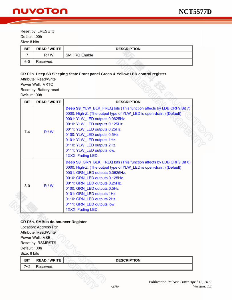
NCT5577D
Publication Release Date: April 13, 2011 -276- Version: 1.1
Reset by: LRESET# Default : 00h Size: 8 bits
BIT READ / WRITE DESCRIPTION
7 R / W SMI IRQ Enable
6-0 Reserved.
CR F2h. Deep S3 Sleeping State Front panel Green & Yellow LED control register Attribute: Read/Write Power Well: VRTC Reset by: Battery reset Default : 00h
BIT READ / WRITE DESCRIPTION
7-4 R / W
Deep S3_YLW_BLK_FREQ bits (This function affects by LDB CRF9 Bit 7)0000: High-Z. (The output type of YLW_LED is open-drain.) (Default) 0001: YLW_LED outputs 0.0625Hz. 0010: YLW_LED outputs 0.125Hz. 0011: YLW_LED outputs 0.25Hz. 0100: YLW_LED outputs 0.5Hz 0101: YLW_LED outputs 1Hz. 0110: YLW_LED outputs 2Hz. 0111: YLW_LED outputs low. 1XXX: Fading LED.
3-0 R / W
Deep S3_GRN_BLK_FREQ bits (This function affects by LDB CRF9 Bit 6)0000: High-Z. (The output type of YLW_LED is open-drain.) (Default) 0001: GRN_LED outputs 0.0625Hz. 0010: GRN_LED outputs 0.125Hz. 0011: GRN_LED outputs 0.25Hz. 0100: GRN_LED outputs 0.5Hz 0101: GRN_LED outputs 1Hz. 0110: GRN_LED outputs 2Hz. 0111: GRN_LED outputs low. 1XXX: Fading LED.
CR F5h. SMBus de-bouncer Register Location: Address F5h Attribute: Read/Write Power Well: VSB Reset by: RSMRST# Default : 00h Size: 8 bits
BIT READ / WRITE DESCRIPTION
7~2 Reserved.

NCT5577D
Publication Release Date: April 13, 2011 -277- Version: 1.1
BIT READ / WRITE DESCRIPTION
1 R / W 1: Enable SCL input de-bouncer 160ns. 0: Disable SCL input de-bouncer.
0 R / W 1: Enable SDA input de-bouncer 160ns. 0: Disable SDA input de-bouncer.
CR F6h. Deep S5 Front Panel Green & Yellow LED control register Attribute: Read/Write Power Well: VRTC Reset by: Battery reset Default : 00h
BIT READ / WRITE DESCRIPTION
7-4 R / W
Deep S5_YLW_BLK_FREQ bits (This function affects by LDB CRF9 Bit 5)0000: High-Z. (The output type of YLW_LED is open-drain.) (Default) 0001: YLW_LED outputs 0.0625Hz. 0010: YLW_LED outputs 0.125Hz. 0011: YLW_LED outputs 0.25Hz. 0100: YLW_LED outputs 0.5Hz 0101: YLW_LED outputs 1Hz. 0110: YLW_LED outputs 2Hz. 0111: YLW_LED outputs low. 1XXX: Fading LED.
3-0 R / W
Deep S5_GRN_BLK_FREQ bits (This function affects by LDB CRF9 Bit 4)0000: High-Z. (The output type of YLW_LED is open-drain.) (Default) 0001: GRN_LED outputs 0.0625Hz. 0010: GRN_LED outputs 0.125Hz. 0011: GRN_LED outputs 0.25Hz. 0100: GRN_LED outputs 0.5Hz 0101: GRN_LED outputs 1Hz. 0110: GRN_LED outputs 2Hz. 0111: GRN_LED outputs low. 1XXX: Fading LED.
CR F7h. Front Panel Green LED (GRN_LED) control register Attribute: Read/Write Power Well: VRTC Reset by: Battery reset Default : 87h
BIT READ / WRITE DESCRIPTION
7 R / W
AUTO_EN (Powered by VSB, RSMRST# reset , default = 1) 0: GRN_LED and YLW_LED are controlled by GRN_ LED_ RST,
GRN_BLK_FREQ and YLW_LED_RST, YLW_BLK_FREQ bits. 1: GRN_LED and YLW_LED are controlled by “SLP_S5#” and “SLP_S3#”.

NCT5577D
Publication Release Date: April 13, 2011 -278- Version: 1.1
BIT READ / WRITE DESCRIPTION
6 R / W GRN_LED_RST# (Default= 0) 0: GRN_BLK_FREQ will be set to “0000” (High-Z) when into S3~S5 state. 1: GRN_BLK_FREQ will be kept when into S3~S5 state.
5 R / W GRN_LED_POL 0: GRN_LED output is active low. (Default) 1: GRN_LED output is active high.
4 Reserved.
3-0 R / W
GRN_BLK_FREQ bits (The reset depends on bit6, GRN_LED_RST#) 0000: High-Z. (The output type of YLW_LED is open-drain.) 0001: GRN_LED outputs 0.0625Hz. 0010: GRN_LED outputs 0.125Hz. 0011: GRN_LED outputs 0.25Hz. 0100: GRN_LED outputs 0.5Hz 0101: GRN_LED outputs 1Hz. 0110: GRN_LED outputs 2Hz. 0111: GRN_LED outputs low. (Default) 1XXX: Fading LED.
CR F8h. Front Panel Yellow LED (YLW_LED) control register Attribute: Read/Write Power Well: VRTC Reset by: Battery reset Default : 47h
BIT READ / WRITE DESCRIPTION
7 Reserved.
6 R / W YLW_LED_RST# (Default =1) 0: YLW_BLK_FREQ will be set to “0000” (High-Z) when into S3~S5 state. 1: YLW_BLK_FREQ will be kept when into S3~S5 state.
5 R / W YLW_LED_POL 0: YLW_LED output is active low. (Default) 1: YLW_LED output is active high.
4 Reserved.
3-0 R / W
YLW_BLK_FREQ bits (The reset depends on bit6,YLW_LED_RST#) 0000: High-Z. (The output type of YLW_LED is open-drain.) 0001: YLW_LED outputs 0.0625Hz. 0010: YLW_LED outputs 0.125Hz. 0011: YLW_LED outputs 0.25Hz. 0100: YLW_LED outputs 0.5Hz 0101: YLW_LED outputs 1Hz. 0110: YLW_LED outputs 2Hz. 0111: YLW_LED outputs low. (Default) 1XXX: Fading LED.
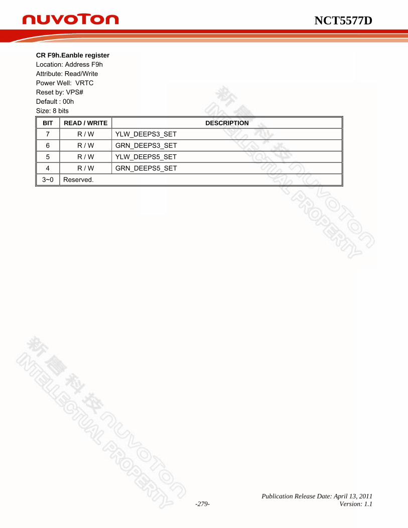
NCT5577D
Publication Release Date: April 13, 2011 -279- Version: 1.1
CR F9h.Eanble register Location: Address F9h Attribute: Read/Write Power Well: VRTC Reset by: VPS# Default : 00h Size: 8 bits
BIT READ / WRITE DESCRIPTION
7 R / W YLW_DEEPS3_SET
6 R / W GRN_DEEPS3_SET
5 R / W YLW_DEEPS5_SET
4 R / W GRN_DEEPS5_SET
3~0 Reserved.

NCT5577D
Publication Release Date: April 13, 2011 -280- Version: 1.1
Logical Device E (CIR WAKE-UP) CR 30h. Location: Address 00h Attribute: Read/Write Power Well: VCC Reset by: LRESET# Default : 00h Size: 8 bits
BIT READ / WRITE DESCRIPTION
7~1 Reserved.
0 R / W 0: CIR Wake-up is inactive. 1: CIR Wake-up Interface is active.
CR 60h, 61h. Location: Address 60h, 61h Attribute: Read/Write Power Well: VCC Reset by: LRESET# Default : 00h, 00h Size: 16 bits
BIT READ / WRITE DESCRIPTION
7~0 R / W These two registers select CIR Wake-up Interface I/O base address <100h: FF8h> on 1 byte boundary.
CR 70h. Location: Address 70h Attribute: Read/Write Power Well: VCC Reset by: LRESET# Default : 00h Size: 8 bits
BIT READ / WRITE DESCRIPTION
7~4 Reserved.
3~0 R / W These bits select IRQ resource for CIR Wake-up.

NCT5577D
Publication Release Date: April 13, 2011 -281- Version: 1.1
19.11 Logical Device F ((GPIO Push-pull or Open-drain selection) CR E1h. Location: Address E1h Attribute: Read/Write Power Well: VSB Reset by: GP2X_MRST Default : DFh Size: 8 bits
BIT READ / WRITE DESCRIPTION
7~0 R / W GP2 Push-Pull/OD select 0:Push-Pull 1:Open Drain
CR E2h. Location: Address E2h Attribute: Read/Write Power Well: VSB Reset by: GP3X_MRST Default : F7h Size: 8 bits
BIT READ / WRITE DESCRIPTION
7~0 R / W GP3 Push-Pull/OD select 0:Push-Pull (Push-Pull is the default for GP33) 1:Open Drain
CR E3h. Location: Address E3h Attribute: Read/Write Power Well: VSB Reset by: GP4X_MRST Default : FEh Size: 8 bits
BIT READ / WRITE DESCRIPTION
7~0 R / W GP4 Push-Pull/OD select 0:Push-Pull 1:Open Drain
CR E4h. Location: Address E4h Attribute: Read/Write Power Well: VSB Reset by: GP5X_MRST Default : F6h Size: 8 bits

NCT5577D
Publication Release Date: April 13, 2011 -282- Version: 1.1
BIT READ / WRITE DESCRIPTION
7~0 R / W GP5 Push-Pull/OD select 0:Push-Pull (Push-Pull is the default for GP52) 1:Open Drain
CR E6h. Location: Address E6h Attribute: Read/Write Power Well: VSB Reset by: GP7X_MRST Default : FFh Size: 8 bits
BIT READ / WRITE DESCRIPTION
7~0 R / W GP7 Push-Pull/OD select 0:Push-Pull 1:Open Drain
CR E7h. Location: Address E7h Attribute: Read/Write Power Well: VSB Reset by: GP8X_MRST Default : D3h Size: 8 bits
BIT READ / WRITE DESCRIPTION
7~0 R / W GP8 Push-Pull/OD select 0:Push-Pull 1:Open Drain
CR E8h. Location: Address E8h Attribute: Read/Write Power Well: VSB Reset by: GP9X_MRST Default : FFh Size: 8 bits
BIT READ / WRITE DESCRIPTION
7~0 R / W GP9 Push-Pull/OD select 0:Push-Pull 1:Open Drain
CR F0h. I2C Control & Address Register Location: Address F0h Attribute: Read/Write
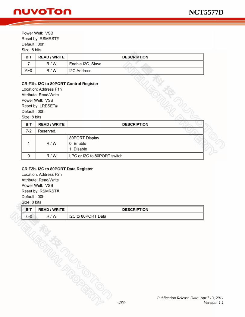
NCT5577D
Publication Release Date: April 13, 2011 -283- Version: 1.1
Power Well: VSB Reset by: RSMRST# Default : 00h Size: 8 bits
BIT READ / WRITE DESCRIPTION
7 R / W Enable I2C_Slave
6~0 R / W I2C Address
CR F1h. I2C to 80PORT Control Register Location: Address F1h Attribute: Read/Write Power Well: VSB Reset by: LRESET# Default : 00h Size: 8 bits
BIT READ / WRITE DESCRIPTION
7-2 Reserved.
1 R / W 80PORT Display 0: Enable 1: Disable
0 R / W LPC or I2C to 80PORT switch
CR F2h. I2C to 80PORT Data Register Location: Address F2h Attribute: Read/Write Power Well: VSB Reset by: RSMRST# Default : 00h Size: 8 bits
BIT READ / WRITE DESCRIPTION
7~0 R / W I2C to 80PORT Data
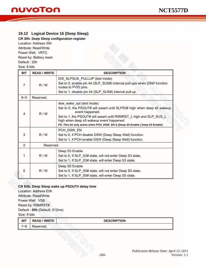
NCT5577D
Publication Release Date: April 13, 2011 -284- Version: 1.1
19.12 Logical Device 16 (Deep Sleep) CR 30h. Deep Sleep configuration register Location: Address 30h Attribute: Read/Write Power Well: VRTC Reset by: Battery reset Default : 20h Size: 8 bits
BIT READ / WRITE DESCRIPTION
7 R / W
DIS_SLPSUS_PULLUP (test mode) Set to 0, enable pin 44 (SLP_SUS#) internal pull-ups when DSW function routes to PVID pins. Set to 1, disable pin 44 (SLP_SUS#) internal pull-up.
6~5 Reserved.
4 R / W
dsw_wake_opt (test mode) Set to 0, the PSOUT# will assert until SLPS3# high when deep s5 wakeup
event happened. Set to 1, the PSOUT# will assert until RSMRST_L high and SLP_SUS_L high when deep s5 wakeup event happened. PS. This bit only active when PCH_DSW_EN & (Deep S5 Enable | Deep S3 Enable)
3 R / W PCH_DSW_EN Set to 0, if PCH disable DSW (Deep Sleep Well) function. Set to 1, if PCH enable DSW (Deep Sleep Well) function.
2 Reserved.
1 R / W Deep S3 Enable Set to 0, If SLP_S3# state, will not enter Deep S3 state. Set to 1, If SLP_S3# state, will enter Deep S3 state.
0 R / W Deep S5 Enable Set to 0, If SLP_S5# state, will not enter Deep S5 state. Set to 1, If SLP_S5# state, will enter Deep S5 state.
CR E0h. Deep Sleep wake up PSOUT# delay time Location: Address E0h Attribute: Read/Write Power Well: VSB Reset by: RSMRST# Default : 20h (Default: 512ms) Size: 8 bits
BIT READ / WRITE DESCRIPTION
7~6 Reserved.

NCT5577D
Publication Release Date: April 13, 2011 -285- Version: 1.1
BIT READ / WRITE DESCRIPTION
5~0 R / W
Deep Sleep wake up PSOUT# delay time. When system wake up from deep sleep state, IO will issue a low pulse via PSOUT# after SYS_3VSB and wait a delay time. DELAY TIME = (Setting Value) * 16ms Example : maximum delay time = (3F)hex * 16ms = 1008ms
CR E1h. Deep Sleep wake up PSOUT# pulse width Location: Address E1h Attribute: Read/Write Power Well: VSB Reset by: RSMRST# Default : 04h (Default: 128 ms) Size: 8 bits
BIT READ / WRITE DESCRIPTION
7~4 Reserved.
3~0 R / W
Deep Sleep wake up PSOUT# pulse width. When system wake up from deep sleep state, IO will issue a low pulse via PSOUT#.. Pulse Width = (Setting Value) * 32ms Example : maximum pulse width = (F)hex * 32ms = 480ms
CR E2h. Deep Sleep Delay Time Control Location: Address E2h Attribute: Read/Write Power Well: VSB Reset by: RSMRST# Default : 05h (Default: 5 sec) Size: 8 bits
BIT READ / WRITE DESCRIPTION
7 R / W 0: The unit of deep sleep delay time is second. 1: The unit of deep sleep delay time is Minute.
6~0 R / W
Deep Sleep Delay Time Control. When system leaves S0 State, IO will wait a delay time before entering into Deep Sleep State. Example: maximum delay time = 127 second/minute
CR E3h. Reserved
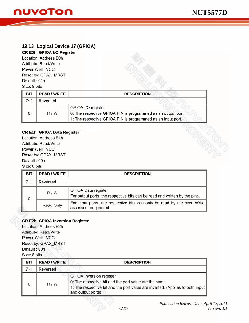
NCT5577D
Publication Release Date: April 13, 2011 -286- Version: 1.1
19.13 Logical Device 17 (GPIOA) CR E0h. GPIOA I/O Register Location: Address E0h Attribute: Read/Write Power Well: VCC Reset by: GPAX_MRST Default : 01h Size: 8 bits
BIT READ / WRITE DESCRIPTION
7~1 Reversed
0 R / W GPIOA I/O register 0: The respective GPIOA PIN is programmed as an output port 1: The respective GPIOA PIN is programmed as an input port.
CR E1h. GPIOA Data Register Location: Address E1h Attribute: Read/Write Power Well: VCC Reset by: GPAX_MRST Default : 00h Size: 8 bits
BIT READ / WRITE DESCRIPTION
7~1 Reversed
R / W GPIOA Data register For output ports, the respective bits can be read and written by the pins.
0 Read Only For Input ports, the respective bits can only be read by the pins. Write
accesses are ignored.
CR E2h. GPIOA Inversion Register Location: Address E2h Attribute: Read/Write Power Well: VCC Reset by: GPAX_MRST Default : 00h Size: 8 bits
BIT READ / WRITE DESCRIPTION
7~1 Reversed
0 R / W
GPIOA Inversion register 0: The respective bit and the port value are the same. 1: The respective bit and the port value are inverted. (Applies to both input and output ports)

NCT5577D
Publication Release Date: April 13, 2011 -287- Version: 1.1
CR E3h. GPIOA Status Register Location: Address E3h Attribute: Read Only Power Well: VCC Reset by: GPAX_MRST Default : 00h Size: 8 bits
BIT READ / WRITE DESCRIPTION
7~1 Reversed
0 Read Only Read-Clear
GPIOA Event Status Bit 7-0 corresponds to GPA7-GPA0, respectively. 0 : No active edge (rising/falling) has been detected 1 : An active edge (rising/falling) has been detected Read the status bit clears it to 0.
CR E4h. GPIOA PUSH-PULL/OD Register Location: Address E4h Attribute: Read/Write Power Well: VCC Reset by: GPAX_MRST Default : 01h Size: 8 bits
BIT READ / WRITE DESCRIPTION
7~1 Reversed
0 R / W GPA Push-Pull/OD select 0:Push-Pull 1:Open Drain
CR E5h. GPIOA Multi-function Select Register Attribute: Read/Write Power Well: VCC Reset by: GPAX_MRST Default : 00h
BIT READ / WRITE DESCRIPTION
7-1 Reversed
0 R / W 0:GPIOA0 1:GPIOA0 WDTO

NCT5577D
Publication Release Date: April 13, 2011 -288- Version: 1.1
20. SPECIFICATIONS
20.1 Absolute Maximum Ratings SYMBOL PARAMETER RATING UNIT
3VCC Power Supply Voltage (3.3V) -0.3 to 3.6 V Input Voltage -0.3 to 3VCC+0.3 V
VI Input Voltage (5V tolerance) -0.3 to 5.5 V
TA Operating Temperature 0 to +70 °C
TSTG Storage Temperature -55 to +150 °C
Note: Exposure to conditions beyond those listed under Absolute Maximum Ratings may adversely affect the life and reliability of the device.
20.2 DC CHARACTERISTICS (TA = 0°C to +70°C, VDD = 3.3V ± 5%, VSS = 0V)
PARAMETER SYM MIN TYP MAX. UNIT CONDITIONS
Battery Quiescent Current IBAT 2.4 μA VBAT = 2.5 V
ACPI Stand-by Power Supply Quiescent Current IVSB 8.0 mA
VSB = 3.3 V, All ACPI pins are not connected.
VCC Quiescent Current IVCC 25 mA
VSB = 3.3 V VCC (AVCC)= 3.3 V LRESET = High IOCLK = 48MHz CASEOPEN Pull-Up to VBAT
Vtt Quiescent Current IVTT 1 mA
VSB = 3.3 V VCC (AVCC)= 3.3 V VTT = 1.2V LRESET = High IOCLK = 48MHz CASEOPEN Pull-Up to VBAT
AIN – Analog input
AOUT – Analog output
INtp3 – 3.3V TTL-level input pin
NCT5577D
Publication Release Date: April 13, 2011 -289- Version: 1.1
PARAMETER SYM MIN TYP MAX. UNIT CONDITIONS
Input Low Voltage VIL 0.8 V
Input High Voltage VIH 2.0 V
Input High Leakage ILIH +10 μA VIN = 3.3V
Input Low Leakage ILIL -10 μA VIN = 0 V
INtsp3 – 3.3V TTL-level, Schmitt-trigger input pin
Input Low Threshold Voltage Vt- 0.5 0.8 1.1 V VCC = 3.3 V
Input High Threshold Voltage Vt+ 1.6 2.0 2.4 V VCC = 3.3 V
Hystersis VTH 0.5 1.2 V VCC = 3.3 V
Input High Leakage ILIH +10 μA VIN = 3.3 V
Input Low Leakage ILIL -10 μA VIN = 0 V
INgp5 – 5V GTL-level input pin
Input Low Voltage VIL 0.72 V
Input High Voltage VIH 0.72 V
Input High Leakage ILIH +10 μA VIN = 3.3V
Input Low Leakage ILIL -10 μA VIN = 0 V
INtp5 – 5V TTL-level input pin
Input Low Voltage VIL 0.8 V
Input High Voltage VIH 2.0 V
Input High Leakage ILIH +10 μA VIN = 3.3V
Input Low Leakage ILIL -10 μA VIN = 0 V
INtscup5 – 5V TTL-level, Schmitt-trigger input buffer with controllable pull-up
Input Low Threshold Voltage Vt- 0.5 0.8 1.1 V VCC = 3.3 V
Input High Threshold Voltage Vt+ 1.6 2.0 2.4 V VCC = 3.3 V
Hystersis VTH 0.5 1.2 V VCC = 3.3 V
Input High Leakage ILIH +10 μA VIN = 3.3 V
Input Low Leakage ILIL -10 μA VIN = 0 V
INtsp5 – 5V TTL-level, Schmitt-trigger input pin
Input Low Threshold Voltage Vt- 0.5 0.8 1.1 V VCC = 3.3 V
Input High Threshold Voltage Vt+ 1.6 2.0 2.4 V VCC = 3.3 V
Hystersis VTH 0.5 1.2 V VCC = 3.3 V
Input High Leakage ILIH +10 μA VIN = 3.3 V
Input Low Leakage ILIL -10 μA VIN = 0 V
INtdp5 – 5V TTL-level input pin with internal pull-down resistor
Input Low Voltage VIL 0.8 V
Input High Voltage VIH 2.0 V
NCT5577D
Publication Release Date: April 13, 2011 -290- Version: 1.1
PARAMETER SYM MIN TYP MAX. UNIT CONDITIONS
Input High Leakage ILIH +10 μA VIN = 3.3V
Input Low Leakage ILIL -10 μA VIN = 0 V
O8 – Output pin with 8mA source-sink capability Output Low Voltage VOL 0.4 V IOL = 8 mA
Output High Voltage VOH 2.4 V IOH = -8 mA
OD8 – Open-drain output pin with 8mA sink capability
Output Low Voltage VOL 0.4 V IOL = 8 mA
O12 – Output pin with 12mA source-sink capability Output Low Voltage VOL 0.4 V IOL = 12 mA
Output High Voltage VOH 2.4 V IOH = -12 mA
OD12 – Open-drain output pin with 12mA sink capability
Output Low Voltage VOL 0.4 V IOL = 12 mA
O24 – Output pin with 24mA source-sink capability Output Low Voltage VOL 0.4 V IOL = 24 mA
Output High Voltage VOH 2.4 V IOH = -24 mA
OD24 – Open-drain output pin with 24mA sink capability
Output Low Voltage VOL 0.4 V IOL = 24 mA
O48 – Output pin with 48mA source-sink capability Output Low Voltage VOL 0.4 V IOL = 48 mA
Output High Voltage VOH 2.4 V IOH = -48 mA
OD48 – Open-drain output pin with 48mA sink capability
Output Low Voltage VOL 0.4 V IOL = 48 mA
I/OV3 – Bi-direction pin with source capability of 6 mA and sink capability of 1 mA for INTEL® PECI
Input Low Voltage VIL 0.275*Vtt 0.5*Vtt V
Input High Voltage VIH 0.55*Vtt 0.725*Vtt V
Output Low Voltage VOL 0.25*Vtt V
Output High Voltage VOH 0.75*Vtt V
Hysterisis VHys 0.1*Vtt V
O12cu – Output pin 12mA source-sink capability with controllable pull-up Output Low Voltage VOL 0.4 V IOL = 12 mA
Output High Voltage VOH 2.4 V IOH = -12 mA
OD12cu – Open-drain 12mA sink capability output pin with controllable pull-up
Output Low Voltage VOL 0.4 V IOL = 12 mA

NCT5577D
Publication Release Date: April 13, 2011 -291- Version: 1.1
21. AC CHARACTERISTICS
21.1 Power On / Off Timing
PSON#
SLP_S3#(Intel Chipset)
S3#(Other Chipset)
PSOUT#
PSIN#
3VSB
T3 T4
T1
T2
S0 S5S5G3
T1 T2 T3 T4
IDEAL TIMING 64ms Over 64ms at least < 10ns 32ms
NCT5577D
Publication Release Date: April 13, 2011 -292- Version: 1.1
21.2 AC Power Failure Resume Timing (1) Logical Device A, CR [E4h] bits [6:5] =00 means “OFF” state
(“OFF” means the system is always turned off after the AC power loss recovered.) 3VCC
PSOUT#
PSON#
SLP_S3#
RSMRST#
3VSB
ACLOSS

NCT5577D
Publication Release Date: April 13, 2011 -293- Version: 1.1
(2) Logical Device A, CR [E4h] bits [6:5]=01 means “ON” state. (“ON” means the system is always turned on after AC power loss recovered.)
3VCC
PSOUT#
PSON#
SLP_S3#
RSMRST#
3VSB
ACLOSS
NCT5577D
Publication Release Date: April 13, 2011 -294- Version: 1.1
** What’s the definition of former state at AC power failure? 1) The previous state is “ON” VCC falls to 2.6V and SLP_S3# keeps at VIH 2.0V
3VCC
SLP_S3#
2) The previous state is “OFF” VCC fall to 2.6V and SLP_S3# keeps at VIL 0.8V
3VCC
SLP_S3#
To ensure that VCC does not fall faster than VSB in various ATX Power Supplies, the NCT5577D adds the option of “user define mode” for the pre-defined state before AC power failure. BIOS can set the pre-defined state for the system to be “On” or “Off”. According to this setting, the system chooses the state after the AC power recovery. Please refer to the descriptions of bit 6~5 of CR E4h and bit 4 of CR E6h in Logical Device A.
CR E4h BIT READ/WRITE DESCRIPTION
6~5 R / W
Power-loss control bits => (VBAT) 0 0: System always turns off when it returns from power-loss state. 0 1: System always turns on when it returns from power-loss state. 1 0: System turns off / on when it returns from power-loss state depending
on the state before the power loss. 1 1: User defines the resuming state before power loss.(refer to Logic
Device A, CRE6[4])
CR E6h
BIT READ/WRITE DESCRIPTION
4 R / W Power loss Last State Flag. (VBAT) 0: ON 1: OFF
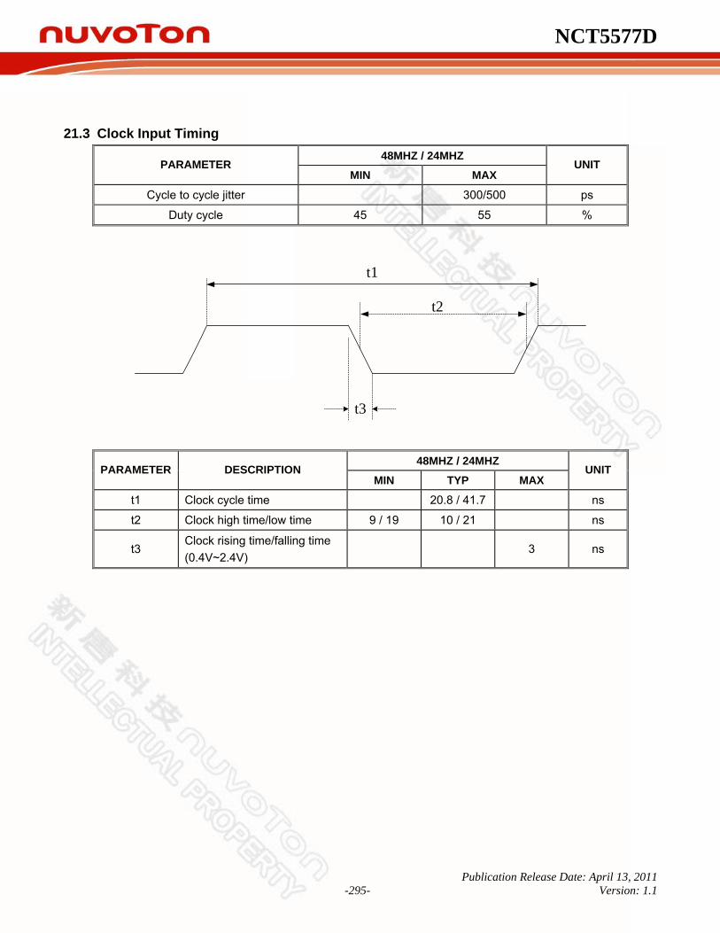
NCT5577D
Publication Release Date: April 13, 2011 -295- Version: 1.1
21.3 Clock Input Timing 48MHZ / 24MHZ
PARAMETER MIN MAX
UNIT
Cycle to cycle jitter 300/500 ps
Duty cycle 45 55 %
t1
t2
t3
48MHZ / 24MHZ PARAMETER DESCRIPTION
MIN TYP MAX UNIT
t1 Clock cycle time 20.8 / 41.7 ns
t2 Clock high time/low time 9 / 19 10 / 21 ns
t3 Clock rising time/falling time (0.4V~2.4V)
3 ns
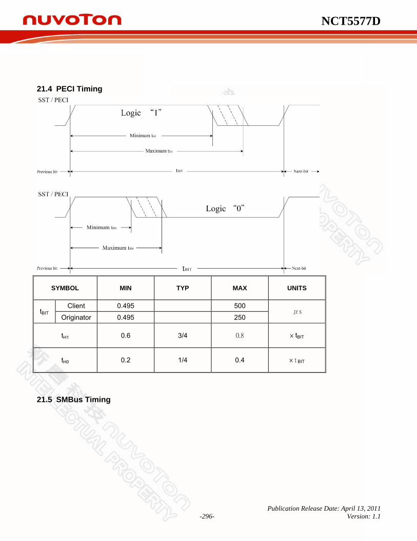
NCT5577D
Publication Release Date: April 13, 2011 -296- Version: 1.1
21.4 PECI Timing
SYMBOL MIN TYP MAX UNITS
Client 0.495 500 tBIT
Originator 0.495 250 μs
tH1 0.6 3/4 0.8 × tBIT
tH0 0.2 1/4 0.4 × t BIT
21.5 SMBus Timing

NCT5577D
Publication Release Date: April 13, 2011 -297- Version: 1.1
SMBCLK
SMBDAT
P S PS
TBUF
THD:STA
TLOW TR
THD:DAT
THIGH
TF
TSU:DAT
TSU:STATSU:STO
21.6 UART PARAMETER SYMBOL TEST
CONDITIONS MIN. MAX. UNIT
Delay from Stop to Set Interrupt TSINT 9/16 Baud Rate
Delay from IOR Reset Interrupt TRINT 9 1000 nS
Delay from Initial IRQ Reset to Transmit Start
TIRS 1/16 8/16 Baud Rate
Delay from to Reset interrupt THR 175 nS
Delay from Initial IOW to interrupt TSI 9/16 16/16 Baud Rate
Delay from Stop to Set Interrupt TSTI 8/16 Baud Rate
Delay from IOR to Reset Interrupt TIR 8 250 nS
Delay from IOR to Output TMWO 6 200 nS
Set Interrupt Delay from Modem Input
TSIM 18 250 nS
Reset Interrupt Delay from IOR TRIM 9 250 nS
Baud Divisor N 100 pF Loading 216-1
UART Receiver Timing
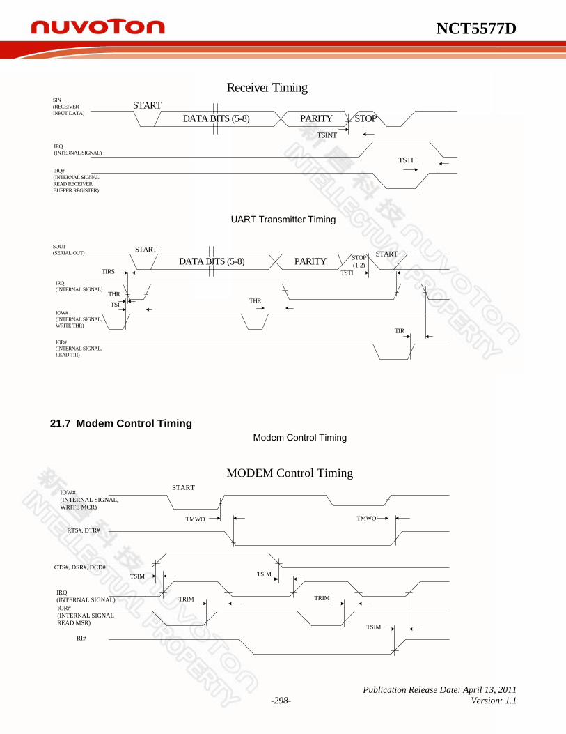
NCT5577D
Publication Release Date: April 13, 2011 -298- Version: 1.1
DATA BITS (5-8) PARITY STOPSTART
TSINT
TSTI
Receiver TimingSIN (RECEIVERINPUT DATA)
IRQ(INTERNAL SIGNAL)
IRQ#(INTERNAL SIGNAL.READ RECEIVERBUFFER REGISTER)
UART Transmitter Timing
DATA BITS (5-8) PARITY STOP(1-2)
START
TSTI
TIR
TIRS
THR
TSI THR
STARTSOUT (SERIAL OUT)
IRQ(INTERNAL SIGNAL)
IOW#(INTERNAL SIGNAL,WRITE THR)
IOR#(INTERNAL SIGNAL,READ TIR)
21.7 Modem Control Timing Modem Control Timing
TSIM
TRIM
TMWO
TSIM
TRIM
TSIM
TMWO
STARTIOW#(INTERNAL SIGNAL,WRITE MCR)
RTS#, DTR#
CTS#, DSR#, DCD#
IRQ(INTERNAL SIGNAL)IOR#(INTERNAL SIGNALREAD MSR)
RI#
MODEM Control Timing

NCT5577D
Publication Release Date: April 13, 2011 -299- Version: 1.1
21.8 KBC Timing Parameters NO. DESCRIPTION MIN. MAX. UNIT
T1 Address Setup Time from WRB 0 nS
T2 Address Setup Time from RDB 0 nS
T3 WRB Strobe Width 20 nS
T4 RDB Strobe Width 20 nS
T5 Address Hold Time from WRB 0 nS
T6 Address Hold Time from RDB 0 nS
T7 Data Setup Time 50 nS
T8 Data Hold Time 0 nS
T9 Gate Delay Time from WRB 10 30 nS
T10 RDB to Drive Data Delay 40 nS
T11 RDB to Floating Data Delay 0 20 nS
T12 Data Valid After Clock Falling (SEND) 4 μS
T13 K/B Clock Period 20 μS
T14 K/B Clock Pulse Width 10 μS
T15 Data Valid Before Clock Falling (RECEIVE) 4 μS
T16 K/B ACK After Finish Receiving 20 μS
T19 Transmit Timeout 2 mS
T20 Data Valid Hold Time 0 μS
T21 Input Clock Period (6−16 Mhz) 63 167 nS
T22 Duration of CLK inactive 30 50 μS
T23 Duration of CLK active 30 50 μS
T24 Time from inactive CLK transition, used to time when the auxiliary device sample DATA
5 25 μS
T25 Time of inhibit mode 100 300 μS
T26 Time from rising edge of CLK to DATA transition 5 T28-5 μS
T27 Duration of CLK inactive 30 50 μS
T28 Duration of CLK active 30 50 μS
T29 Time from DATA transition to falling edge of CLK 5 25 μS
21.8.1 Writing Cycle Timing
Write Cycle Timing
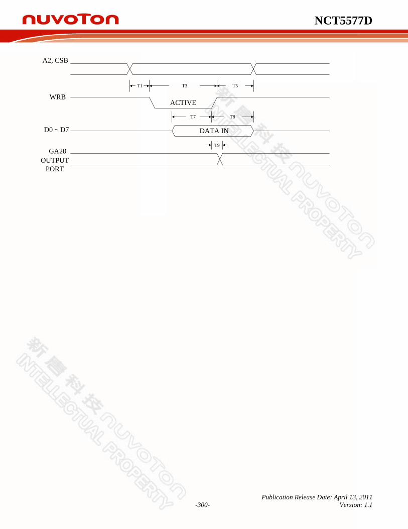
NCT5577D
Publication Release Date: April 13, 2011 -300- Version: 1.1
T7 T8
T9
T3T1 T5
A2, CSB
WRB
D0 ~ D7
GA20OUTPUT
PORT
DATA IN
ACTIVE

NCT5577D
Publication Release Date: April 13, 2011 -301- Version: 1.1
21.8.2 Read Cycle Timing
Read Cycle
T10 T11
T2 T4T6
ACTIVE
DATA OUT
A2, CSB
AEN
RDB
D0 ~ D7
21.8.3 Send Data to K/B Send Data to K/B
START STOPD0 D1 D2 D3 D4 D5 D6 D7 P
CLOCK(KCLK)
SERIAL DATA(KDAT)
T12T14 T13 T26
21.8.4 Receive Data from K/B Receive Data from K/B
T15T14 T13
START STOPD0 D1 D2 D3 D4 D5 D6 D7 P
CLOCK(KCLK)
SERIAL DATA(T1)
T20
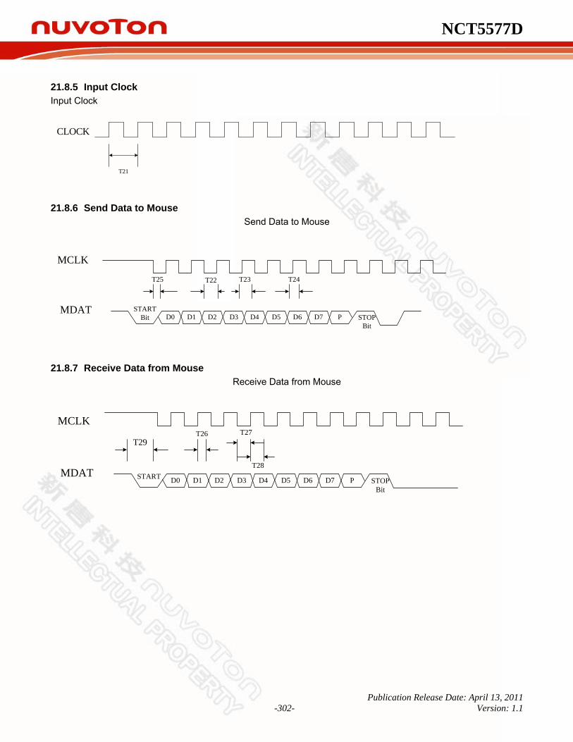
NCT5577D
Publication Release Date: April 13, 2011 -302- Version: 1.1
21.8.5 Input Clock Input Clock
T21
CLOCK
21.8.6 Send Data to Mouse Send Data to Mouse
STARTBit STOP
BitD0 D1 D2 D3 D4 D5 D6 D7 P
MCLK
MDAT
T25 T22 T23 T24
21.8.7 Receive Data from Mouse Receive Data from Mouse
START STOPBit
D0 D1 D2 D3 D4 D5 D6 D7 P
MCLK
MDAT
T29T26 T27
T28

NCT5577D
Publication Release Date: April 13, 2011 -303- Version: 1.1
21.9 GPIO Timing Parameters SYMBOL PARAMETER MIN. MAX. UNIT
tWGO Write data to GPIO update 300(Note 1) ns
tSWP SWITCH pulse width 16 msec
Note: Refer to Microprocessor Interface Timing for Read Timing.
21.9.1 GPIO Write Timing GPIO Write Timing diagram
VALID
VALID
tWGO
PREVIOUS STATE VALID
A0-A15
IOW
D0-7
GPIO10-17GPIO20-25

NCT5577D
Publication Release Date: April 13, 2011 -304- Version: 1.1
22. TOP MARKING SPECIFICATIONS
1st line: Nuvoton logo 2nd line: part number: NCT5577D (Green package) 3rd line: wafer production series lot number: E902B006 4th line: tracking code 010G9AFA
010: packages made in 2010, week 10 G: assembly house ID; G means GR, A means ASE, etc 9: code version; 9 means code 009 A: IC revision; A means version A; B means version B, and C means version C FA: Nuvoton internal use
NCT5577D E902B006
010G9AFA
NCT5577D
Publication Release Date: April 13, 2011 -305- Version: 1.1
23. ORDERING INFORMATION
PART NUMBER PACKAGE TYPE PRODUCTION FLOW
NCT5577D 64Pin LQFP (Green package) Commercial, 0°C to +70°C

NCT5577D
Publication Release Date: April 13, 2011 -306- Version: 1.1
24. PACKAGE SPECIFICATION

NCT5577D
Publication Release Date: April 13, 2011 -307- Version: 1.1
64-pin (LQFP, 7x7x1.4mm)

NCT5577D
Publication Release Date: April 13, 2011 -308- Version: 1.1
25. REVISION HISTORY
VERSION DATE PAGE DESCRIPTION
0.6 06/09/2010 N.A. Preliminary datasheet
0.7 07/02/2010 N.A. Re-define pin configuration
1.0 02/08/2011 N.A. Update the contents.
1.1 04/13/2011 N.A. Update the contents.

NCT5577D
Publication Release Date: April 13, 2011 -309- Version: 1.1
Important Notice
Nuvoton Products are neither intended nor warranted for usage in systems or equipment, any malfunction or failure of which may cause loss of human life, bodily injury or severe property damage. Such applications are deemed, “Insecure Usage”. Insecure usage includes, but is not limited to: equipment for surgical implementation, atomic energy control instruments, airplane or spaceship instruments, the control or operation of dynamic, brake or safety systems designed for vehicular use, traffic signal instruments, all types of safety devices, and other applications intended to support or sustain life.
All Insecure Usage shall be made at customer’s risk, and in the event that third parties lay claims to Nuvoton as a result of customer’s Insecure Usage, customer shall indemnify the damages and liabilities thus incurred by Nuvoton.
Related Documents