© Semiconductor Components Industries, LLC, 2021 July, 2021 − Rev. P0 1 Publication Order Number: NCP51513/D 130 V, 2.0 A / 3.0 A High and Low Side Drivers with Dead Time & Interlock Product Preview NCP51513 Description NCP51513 is 130 V half bridge driver with high drive current capabilities and options for DC−DC power supplies and inverters. NCP51513 offers best in class propagation delay, low quiescent current and low switching current at high frequencies of operation. This device is tailored for highly efficient power supplies operating at high frequencies. NCP51513 is offered in two versions for propagation delays. With filter version, it has a typical 50 ns propagation delay, while without filter version it has a typical propagation delay of 20 ns. Internal 80 ns dead time and interlock function protect the output MOSFETs against cross conduction events. Enable functionality provides additional system flexibility and helps reducing power consumption. Features • High Voltage Range: Up to 130 V • dV/dt Immunity Up to 50 V/ns • Output Source / Sink Current Capability 2.0 A / 3.0 A • Rise / Fall Time 9 ns / 7 ns for 1 nF Load • Independent Logic Inputs 3.3 V and 5 V Compatible • Enable Input • Propagation Delay 50 ns A Version, 20 ns B Version • Input Filter Time 30 ns for A Version and No Filter for B Version • Internal Fixed 80 ns Dead Time • Input Cross−Conduction Prevention • Extended Allowable Negative Bridge Pin Voltage Swing to −10 V @ Vcc = 10 V • Matched Propagation Delays Between Both Channels Max 11 ns • Independent Under Voltage Lock Out (UVLO) for Both Channels • This is a Pb−Free Device Typical Applications • Half and Full Bridge Converters • DC−to−AC Inverters • Motor Drivers • Synchronous Buck This document contains information on a product under development. ON Semiconductor reserves the right to change or discontinue this product without notice. www. onsemi.com ORDERING INFORMATION MARKING DIAGRAM DFN10 (3x3) CASE 506CL PIN CONNECTION 51513 Pxy ALYW G x = A or B (Input Noise Filter) y = Internal Dead Time 80 ns A = Assembly Location L = Wafer Lot Y = Year W = Work Week G = Pb−Free Package Device Package Shipping † NCP51513ABMNTWG DFN10 (Pb−free) 3000 / Tape & Reel †For information on tape and reel specifications, including part orientation and tape sizes, please refer to our Tape and Reel Packaging Specification Brochure, BRD8011/D. NC VB DRVH VCC LIN DRVL EN 1 2 3 4 5 6 7 8 9 10 GND HIN HB (Note: Microdot may be in either location) Top View

Welcome message from author
This document is posted to help you gain knowledge. Please leave a comment to let me know what you think about it! Share it to your friends and learn new things together.
Transcript

© Semiconductor Components Industries, LLC, 2021
July, 2021 − Rev. P01 Publication Order Number:
NCP51513/D
130 V, 2.0 A / 3.0 AHigh and Low Side Driverswith Dead Time & Interlock
Product Preview
NCP51513
DescriptionNCP51513 is 130 V half bridge driver with high drive current
capabilities and options for DC−DC power supplies and inverters.NCP51513 offers best in class propagation delay, low quiescentcurrent and low switching current at high frequencies of operation.
This device is tailored for highly efficient power supplies operatingat high frequencies. NCP51513 is offered in two versionsfor propagation delays. With filter version, it has a typical 50 nspropagation delay, while without filter version it has a typicalpropagation delay of 20 ns. Internal 80 ns dead time and interlockfunction protect the output MOSFETs against cross conduction events.Enable functionality provides additional system flexibility and helpsreducing power consumption.
Features• High Voltage Range: Up to 130 V
• dV/dt Immunity Up to 50 V/ns
• Output Source / Sink Current Capability 2.0 A / 3.0 A
• Rise / Fall Time 9 ns / 7 ns for 1 nF Load
• Independent Logic Inputs 3.3 V and 5 V Compatible
• Enable Input
• Propagation Delay 50 ns A Version, 20 ns B Version
• Input Filter Time 30 ns for A Version and No Filter for B Version
• Internal Fixed 80 ns Dead Time
• Input Cross−Conduction Prevention
• Extended Allowable Negative Bridge Pin Voltage Swing to −10 V @ Vcc = 10 V
• Matched Propagation Delays Between Both Channels Max 11 ns
• Independent Under Voltage Lock Out (UVLO) for Both Channels
• This is a Pb−Free Device
Typical Applications• Half and Full Bridge Converters
• DC−to−AC Inverters
• Motor Drivers
• Synchronous Buck
This document contains information on a product under development. ON Semiconductorreserves the right to change or discontinue this product without notice.
www.onsemi.com
ORDERING INFORMATION
MARKING DIAGRAM
DFN10 (3x3)CASE 506CL
PIN CONNECTION
51513Pxy
ALYW�
x = A or B (Input Noise Filter)y = Internal Dead Time 80 nsA = Assembly LocationL = Wafer LotY = YearW = Work Week� = Pb−Free Package
Device Package Shipping†
NCP51513ABMNTWG DFN10(Pb−free)
3000 / Tape & Reel
†For information on tape and reel specifications,including part orientation and tape sizes, pleaserefer to our Tape and Reel Packaging SpecificationBrochure, BRD8011/D.
NC
VB
DRVH
VCC
LIN
DRVL
EN
1
2
3
4
5 6
7
8
9
10
GND
HIN
HB
(Note: Microdot may be in either location)
Top View
NCP51513
www.onsemi.com2
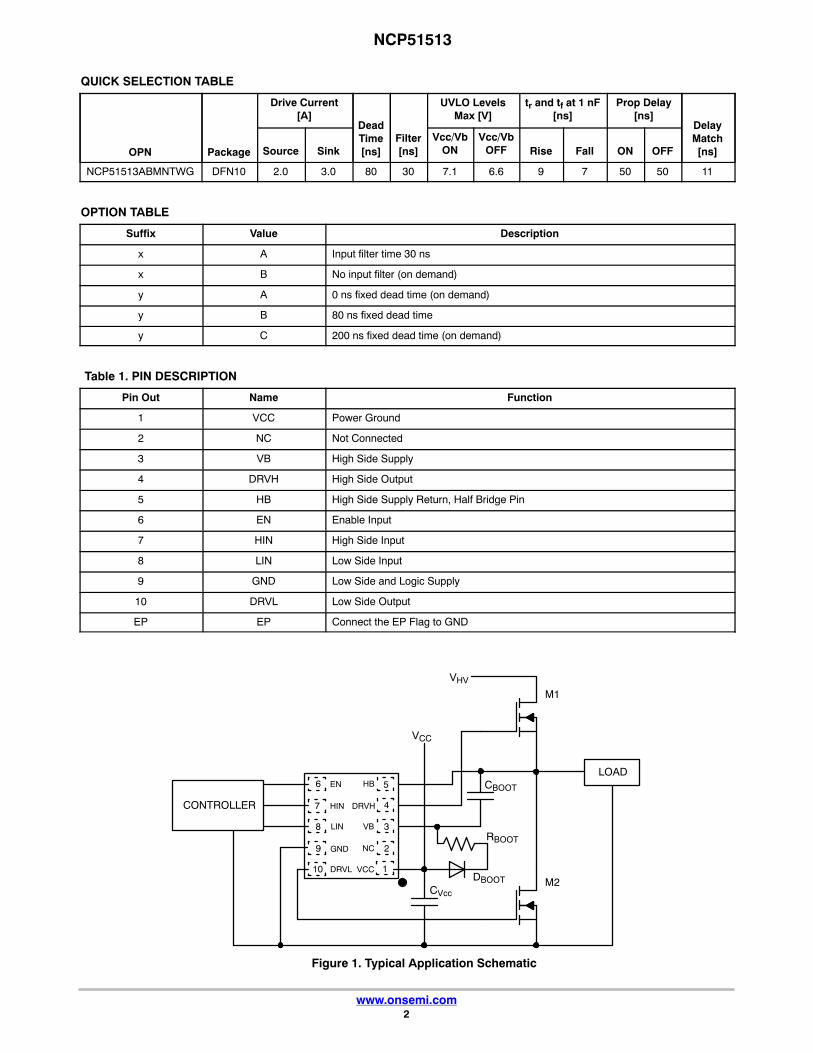
QUICK SELECTION TABLE
OPN Package
Drive Current[A]
DeadTime[ns]
Filter[ns]
UVLO LevelsMax [V]
tr and tf at 1 nF[ns]
Prop Delay[ns]
DelayMatch[ns]Source Sink
Vcc/VbON
Vcc/VbOFF Rise Fall ON OFF
NCP51513ABMNTWG DFN10 2.0 3.0 80 30 7.1 6.6 9 7 50 50 11
OPTION TABLE
Suffix Value Description
x A Input filter time 30 ns
x B No input filter (on demand)
y A 0 ns fixed dead time (on demand)
y B 80 ns fixed dead time
y C 200 ns fixed dead time (on demand)
Table 1. PIN DESCRIPTION
Pin Out Name FunctionÁÁÁÁÁÁÁÁÁÁÁÁÁÁ1
ÁÁÁÁÁÁÁÁÁÁÁÁÁÁVCC
ÁÁÁÁÁÁÁÁÁÁÁÁÁÁÁÁÁÁÁÁÁÁÁÁÁÁÁÁÁÁÁÁÁÁÁÁÁÁÁÁÁÁPower GroundÁÁÁÁÁÁÁ
ÁÁÁÁÁÁÁ2ÁÁÁÁÁÁÁÁÁÁÁÁÁÁNC
ÁÁÁÁÁÁÁÁÁÁÁÁÁÁÁÁÁÁÁÁÁÁÁÁÁÁÁÁÁÁÁÁÁÁÁÁÁÁÁÁÁÁNot ConnectedÁÁÁÁÁÁÁ
ÁÁÁÁÁÁÁ3ÁÁÁÁÁÁÁÁÁÁÁÁÁÁVB
ÁÁÁÁÁÁÁÁÁÁÁÁÁÁÁÁÁÁÁÁÁÁÁÁÁÁÁÁÁÁÁÁÁÁÁÁÁÁÁÁÁÁHigh Side SupplyÁÁÁÁÁÁÁ
ÁÁÁÁÁÁÁ4ÁÁÁÁÁÁÁÁÁÁÁÁÁÁDRVH
ÁÁÁÁÁÁÁÁÁÁÁÁÁÁÁÁÁÁÁÁÁÁÁÁÁÁÁÁÁÁÁÁÁÁÁÁÁÁÁÁÁÁHigh Side OutputÁÁÁÁÁÁÁ
ÁÁÁÁÁÁÁ5ÁÁÁÁÁÁÁÁÁÁÁÁÁÁHB
ÁÁÁÁÁÁÁÁÁÁÁÁÁÁÁÁÁÁÁÁÁÁÁÁÁÁÁÁÁÁÁÁÁÁÁÁÁÁÁÁÁÁHigh Side Supply Return, Half Bridge PinÁÁÁÁÁÁÁ
ÁÁÁÁÁÁÁ6ÁÁÁÁÁÁÁÁÁÁÁÁÁÁEN
ÁÁÁÁÁÁÁÁÁÁÁÁÁÁÁÁÁÁÁÁÁÁÁÁÁÁÁÁÁÁÁÁÁÁÁÁÁÁÁÁÁÁEnable InputÁÁÁÁÁÁÁ
ÁÁÁÁÁÁÁ7ÁÁÁÁÁÁÁÁÁÁÁÁÁÁHIN
ÁÁÁÁÁÁÁÁÁÁÁÁÁÁÁÁÁÁÁÁÁÁÁÁÁÁÁÁÁÁÁÁÁÁÁÁÁÁÁÁÁÁHigh Side InputÁÁÁÁÁÁÁ
ÁÁÁÁÁÁÁ8ÁÁÁÁÁÁÁÁÁÁÁÁÁÁLIN
ÁÁÁÁÁÁÁÁÁÁÁÁÁÁÁÁÁÁÁÁÁÁÁÁÁÁÁÁÁÁÁÁÁÁÁÁÁÁÁÁÁÁLow Side InputÁÁÁÁÁÁÁ
ÁÁÁÁÁÁÁ9ÁÁÁÁÁÁÁÁÁÁÁÁÁÁGND
ÁÁÁÁÁÁÁÁÁÁÁÁÁÁÁÁÁÁÁÁÁÁÁÁÁÁÁÁÁÁÁÁÁÁÁÁÁÁÁÁÁÁLow Side and Logic SupplyÁÁÁÁÁÁÁ
ÁÁÁÁÁÁÁ10ÁÁÁÁÁÁÁÁÁÁÁÁÁÁDRVL
ÁÁÁÁÁÁÁÁÁÁÁÁÁÁÁÁÁÁÁÁÁÁÁÁÁÁÁÁÁÁÁÁÁÁÁÁÁÁÁÁÁÁLow Side OutputÁÁÁÁÁÁÁ
ÁÁÁÁÁÁÁEPÁÁÁÁÁÁÁÁÁÁÁÁÁÁEP
ÁÁÁÁÁÁÁÁÁÁÁÁÁÁÁÁÁÁÁÁÁÁÁÁÁÁÁÁÁÁÁÁÁÁÁÁÁÁÁÁÁÁConnect the EP Flag to GNDÁÁÁÁÁÁÁÁÁÁÁÁÁÁÁÁÁÁÁÁÁÁÁÁÁÁÁÁÁÁÁÁÁ
ÁÁÁÁÁÁÁÁÁÁÁÁÁÁÁÁÁÁÁÁÁÁÁÁÁÁÁÁÁÁÁÁÁ
M1
M2
CONTROLLER
LOADHB
DRVH
VB
NC
EN
HIN
LIN
GND
VCCDRVL
Figure 1. Typical Application Schematic
6
VCC
VHV
CBOOT
RBOOT
DBOOTCVcc
7
8
9
10
5
4
3
2
1

NCP51513
www.onsemi.com3
Figure 2. NCP51513A Version
S
R
Q
Q DRVH
HB
VB
DRVL
HIN
LIN
GND
DELAY
EN
S
R
Q
Q DRVH
HB
VB
DRVL
HIN
LIN
GND
DELAY
EN
Figure 3. NCP51513B Version
VCC
VCC
VCC
VCC
UVDetect
PulseTrigger
LevelShifter
UVDetect
Dead time and Cross conductionprevention logic
UVDetect
PulseTrigger
LevelShifter
Dead time and Cross conductionprevention logic
UVDetect
Inputfilter
Inputfilter
Inputfilter

NCP51513
www.onsemi.com4
MAXIMUM RATINGS
Rating Symbol Value Units
Supply Voltage Range VCC −0.3 to 20 V
High Side Boot Pin Voltage VB −0.3 to 150 V
High Side Floating Voltage VB−VHB −0.3 to 20 V
High Side Bridge Pin Voltage VHB VB −20 to VB + 0.3 V
High Side Drive Output Voltage VDRVH VHB −0.3 to VB + 0.3 V
Low Side Output Voltage VDRVL −0.3 to VCC + 0.3 V
Allowable Output Slew Rate dVHB/dt 50 V/ns
Inputs HIN, LIN VLIN, VHIN −5 to VCC + 0.3 V
Input EN VEN −0.3 to VCC + 0.3 V
Junction Temperature TJ_max +150 °C
Storage Temperature Range TST −55 to +150 °C
ESD Capability (Note 1):− HBM Model− CDM Model
20001000
VV
Lead Temperature SolderingReflow (SMD Styles ONLY), Pb−Free Versions (Note 2)
260 °C
Stresses exceeding those listed in the Maximum Ratings table may damage the device. If any of these limits are exceeded, device functionalityshould not be assumed, damage may occur and reliability may be affected.1. This device series incorporates ESD protection and is tested by the following methods. ESD Human Body Model tested
perAEC−Q100−002(EIA/JESD22−A114)ESD Charged Device Model tested per AEC−Q100−11(EIA/JESD22−C101E)Latchup Current Maximum Rating: ≤100 mA per JEDEC standard: JESD78E.
2. For information, please refer to our Soldering and Mounting Techniques Reference Manual, SOLDERRM/D.
THERMAL CHARACTERISTICS
Rating Symbol Value Units
Thermal Resistance Junction to Air (Note 3) RθJA 157 °C/W
Junction to Top Characterization Parameter �J−T 8.5 °C/W
Junction to Bottom Characterization Parameter �J−B 0.12 °C/W
3. Values based on copper area of 100 mm2 1 oz copper thickness and FR4 PCB substrate
RECOMMENDED OPERATING CONDITIONS
Rating Symbol Min Max Unit
Supply Voltage Range VCC 8 19 V
Floating Supply Voltage Range VB−VHB 8 19 V
Bridge Pin Voltage Range @ Vcc = 10 V VHB −2 110 V
High Side Driver Voltage VDRVH VHB VB V
Low Side Driver Voltage VDRVL GND VCC V
Input Signal Voltage VHIN, VLIN −3 VCC V
Input Signal Voltage VEN GND VCC V
Operating Junction Temperature Range TJ −40 +125 °C
Functional operation above the stresses listed in the Recommended Operating Ranges is not implied. Extended exposure to stresses beyondthe Recommended Operating Ranges limits may affect device reliability.

NCP51513
www.onsemi.com5
ELECTRICAL CHARACTERISTICS (VCC = VB = 12 V, VGND = VHB, −40°C < Tj < 125°C, Outputs loaded with 1 nF, typical values are valid for 25°C. All voltages arereferred to GND pin)
Parameter Symbol Test Condition Min Typ Max Unit
SUPPLY SECTION
VCC Current Consumption in Active Mode ICC1 fSW = 100 kHz − 1.8 2.3 mA
VB Current Consumption in Active Mode IB1 fSW = 100 kHz − 1.8 2.3 mA
VCC Current Consumption in Active Mode ICC1_noload fSW = 100 kHz, CLOAD = 0 − 0.6 1.2 mA
VB Current Consumption in Active Mode IB1−noload fSW = 100 kHz, CLOAD = 0 − 0.3 0.5 mA
Vcc Current Consumption in Active Mode ICC2_EN_H fSW = 0 Hz, VEN = 3 V − 150 250 μA
VB Current Consumption in Active Mode IB2_EN_H fSW = 0 Hz, VEN = 3 V − 100 150 μA
VCC Current Consumption in Inhibition Mode ICC2 VEN = 0 V − 150 250 μA
VB Current Consumption in Inhibition Mode IB2 VEN = 0 V − 100 150 μA
Leakage Current on High Voltage Pins to GND IHV_LEAK VB = HB = DRVH = 130 V − 2 5 μA
INPUT SECTION
Low Level Input Voltage Threshold VxINL, VENL − − 0.8 V
Input Pull−Down Resistor RxIN VxIN = 5 V, VEN = 0 V 100 175 250 k�
High Level Input Voltage Threshold VxINH, VENH 2.3 − − V
Enable Pin Pull−Down Resistor REN VEN = 5 V 60 95 135 k�
Logic “1” Input Bias Current IxIN+ VxIN = 5 V, VEN = 5 V − 30 50 μA
Logic “0” Input Bias Current IxIN− VxIN = 0 V, VEN = 0 V − − 2.0 μA
Logic “1” Input Bias Current IEN+ VEN = 5 V − 50 85 μA
Logic “0” Input Bias Current IEN− VEN = 0 V − − 2.0 μA
UVLO SECTION
VCC UV Start−Up Voltage Threshold VCCon 5.8 6.4 7.0 V
VCC UV Shut−Down Voltage Threshold VCCoff 5.3 5.9 6.5 V
Hysteresis on VCC VCChyst 0.2 0.5 − V
Vboot Start−Up Voltage Threshold Reference toBridge Pin
VBon VBon = VB − HB 5.8 6.4 7.0 V
Vboot UV Shut−Down Voltage Threshold VBoff 5.3 5.9 6.5 V
Hysteresis on Vboot VBhyst 0.2 0.5 − V
Time between Vboot > VBon & 1st DRVH Pulse tstartup − − 10 μs
OUTPUT SECTION
Output High Short Circuit Pulsed Current (Note 4)
IDRVxsource VDRVx = 0 V, PW = 300 ns − 2.0 − A
Output Low Short Circuit Pulsed Current (Note 4)
IDRVxsink VDRVx = VCC (VB), PW = 300 ns − 3.0 − A
Output Resistance Source ROH IDRVx = 30 mA − 2.5 7 �
Output Resistance Sink ROL IDRVx = 30 mA − 1.5 5 �
High Level Output Voltage VDRVx H VBIAS − VDRVx @ IDRVL = 20 mA − 0.06 0.25 V
Low Level Output Voltage VDRVx L VDRVx @ IDRVx = 20 mA − 0.04 0.15 V
OUTPUT RISE AND FALL TIME
Output Voltage Rise Time (from 10% to 90%) tr VxIN = 3 V − 9 30 ns
Output Voltage Fall Time (from 90% to 10%) tf VxIN = 0 V − 7 25 ns

NCP51513
www.onsemi.com6
ELECTRICAL CHARACTERISTICS (continued)(VCC = VB = 12 V, VGND = VHB, −40°C < Tj < 125°C, Outputs loaded with 1 nF, typical values are valid for 25°C. All voltages arereferred to GND pin)
Parameter UnitMaxTypMinTest ConditionSymbol
PROPAGATION DELAY NCP51513A
Turn−On Propagation Delay tON HB = 0 V, 50 V or 130 V, Cload = 0 pF, VxIN = 3 V
− 50 100 ns
Turn−Off Propagation Delay tOFF HB = 0 V, 50 V or 130 V, Cload = 0 pF
− 50 100 ns
Enable High Signal Propagation Delay tEN HB = 0 V, 50 V or 130 V, Cload = 0 pF, VxIN = 3 V
− 50 100 ns
Enable Low Signal Propagation Delay tENoff HB = 0 V, 50 V or 130 V, Cload = 0 pF, VxIN = 3 V
− 50 100 ns
Minimum Input Filter Time tFLT VxIN = 3 V 20 30 − ns
PROPAGATION DELAY NCP51513B
Turn−On Propagation Delay tON HB = 0 V, 50 V or 130 V, Cload = 0 pF, VxIN = 3 V
− 20 40 ns
Turn−Off Propagation Delay tOFF HB = 0 V, 50 V or 130 V, Cload = 0 pF
− 20 40 ns
Enable High Signal Propagation Delay tEN HB = 0 V, 50 V or 130 V, Cload = 0 pF, VxIN = 3 V
− 20 40 ns
Enable Low Signal Propagation Delay tENoff HB = 0 V, 50 V or 130 V, Cload = 0 pF, VxIN = 3 V
− 20 40 ns
DELAY MATCHING
Propagation Delay Matching between the High Side and the Low Side
�t VxIN = 3 V − 0 11 ns
TIMING
Minimum Input Width that Changes the Output tPW VxIN = 3 V (B Version Only)
− − 10 ns
Internal Dead Time tDT VxIN = 3 V 60 80 100 ns
Dead Time Matching �tDT − − 20 ns
Product parametric performance is indicated in the Electrical Characteristics for the listed test conditions, unless otherwise noted. Productperformance may not be indicated by the Electrical Characteristics if operated under different conditions.4. Parameter guaranteed by design.

NCP51513
www.onsemi.com7
Figure 4. Propagation Delay, Propagation Delay Matching,Rise Time and Fall Time Testing
Figure 5. Dead Time and Dead Time Matching Measurement
DRVL(DRVH)
LIN(HIN)
50%
90%
10%
10%
10%
90%
90%
DRVL
DRVH
DRVL
DRVH
tONL(tONH)
trL(trH)
tOFFL(tOFFH)
tfL(tfH)
tON = higher of {tONL, tONH}
tOFF = higher of {tOFFL, tOFFH}
�tA = the highest of {tONL, tONH, tOFFL, tOFFH}
�tB = the lowest of {tONL, tONH, tOFFL, tOFFH}
�t = �tA − �tB
tr = higher of {trL, trH}
tf = higher of {tfL, tfH}
tDT A is in limit of tDTtDT B is in limit of tDT�tDT = ⎪tDT A − tDT B⎪
tDT A tDT B

NCP51513
www.onsemi.com8
TYPICAL ELECTRICAL CHARACTERISTICS
6.30
6.35
6.40
6.45
6.50
−40 −20 0 20 40 60 80 100 120
Vol
tage
[V]
Temperature [°C]
5.90
5.91
5.92
5.93
5.94
5.95
5.96
5.97
5.98
5.99
6.00
−40 −20 0 20 40 60 80 100 120
Vol
tage
[V]
Temperature [°C]
Figure 6. VCCon vs. Temperature Figure 7. VCCoff vs. Temperature
0.40
0.41
0.42
0.43
0.44
0.45
0.46
0.47
0.48
0.49
0.50
−40 −20 0 20 40 60 80 100 120
Vol
tage
[V]
Temperature [°C]
Figure 8. VCChyst vs. Temperature
6.32
6.33
6.34
6.35
6.36
6.37
6.38
6.39
6.40
−40 −20 0 20 40 60 80 100 120
Vol
tage
[V]
Temperature [°C]
Figure 9. VBon vs. Temperature
5.90
5.91
5.92
5.93
5.94
5.95
5.96
5.97
5.98
5.99
6.00
−40 −20 0 20 40 60 80 100 120
Vol
tage
[V]
Temperature [°C]
Figure 10. VBoff vs. Temperature
0.38
0.39
0.40
0.41
0.42
0.43
0.44
0.45
−40 −20 0 20 40 60 80 100 120
Vol
tage
[V]
Temperature [°C]
Figure 11. VBhyst vs. Temperature

NCP51513
www.onsemi.com9
TYPICAL ELECTRICAL CHARACTERISTICS (continued)
1.55
1.57
1.59
1.61
1.63
1.65
−40 −20 0 20 40 60 80 100 120
Cur
rent
[mA
]
Temperature [°C]
Figure 12. ICC1 vs. Temperature
0.230
0.235
0.240
0.245
0.250
0.255
0.260
0.265
0.270
−40 −20 0 20 40 60 80 100 120
Cur
rent
[mA
]
Temperature [°C]
Figure 13. ICC1 noload vs. Temperature
109
111
113
115
117
119
121
123
125
−40 −20 0 20 40 60 80 100 120
Cur
rent
[�A
]
Temperature [°C]
Figure 14. ICC1 EN H vs. Temperature
70
80
90
100
110
120
130
140
150
−40 −20 0 20 40 60 80 100 120
Cur
rent
[�A
]
Temperature [°C]
Figure 15. ICC2 vs. Temperature
1.45
1.47
1.49
1.51
1.53
1.55
−40 −20 0 20 40 60 80 100 120
Cur
rent
[mA
]
Temperature [°C]
Figure 16. IB1 vs. Temperature
0.200
0.205
0.210
0.215
0.220
0.225
0.230
0.235
0.240
0.245
0.250
−40 −20 0 20 40 60 80 100 120
Cur
rent
[mA
]
Temperature [°C]
Figure 17. IB1 noload vs. Temperature

NCP51513
www.onsemi.com10
TYPICAL ELECTRICAL CHARACTERISTICS (continued)
60
65
70
75
80
85
90
95
100
−40 −20 0 20 40 60 80 100 120
Cur
rent
[�A
]
Temperature [°C]
Figure 18. IB1 EN H vs. Temperature
65
70
75
80
85
90
95
−40 −20 0 20 40 60 80 100 120
Cur
rent
[�A
]
Temperature [°C]
Figure 19. IB2 vs. Temperature
150
155
160
165
170
175
180
185
190
195
200
−40 −20 0 20 40 60 80 100 120
Res
istiv
ity [k
�]
Temperature [°C]
Figure 20. RxIH vs. Temperature
100
105
110
115
120
125
130
135
140
145
150
−40 −20 0 20 40 60 80 100 120
Res
istiv
ity [k
�]
Temperature [°C]
Figure 21. REN vs. Temperature
54
56
58
60
62
64
66
68
−40 −20 0 20 40 60 80 100 120
Tim
e [n
s]
Temperature [°C]
Figure 22. tON vs. Temperature
54
56
58
60
62
64
66
−40 −20 0 20 40 60 80 100 120
Tim
e [n
s]
Temperature [°C]
Figure 23. tOFF vs. Temperature

NCP51513
www.onsemi.com11
TYPICAL ELECTRICAL CHARACTERISTICS (continued)
0
1
2
3
4
5
6
−40 −20 0 20 40 60 80 100 120
Tim
e [n
s]
Temperature [°C]
Figure 24. �t vs. Temperature
55
56
57
58
59
60
61
62
63
64
−40 −20 0 20 40 60 80 100 120
Tim
e [n
s]
Temperature [°C]
Figure 25. tEN vs. Temperature
77.0
77.5
78.0
78.5
79.0
79.5
80.0
−40 −20 0 20 40 60 80 100 120
Tim
e [n
s]
Temperature [°C]
Figure 26. tDT vs. Temperature
−12
−10
−8
−6
−4
−2
0
2
4
6
−40 −20 0 20 40 60 80 100 120
Tim
e [n
s]
Temperature [°C]
Figure 27. �tDT vs. Temperature
5
6
7
8
9
10
11
12
13
14
−40 −20 0 20 40 60 80 100 120
Tim
e [n
s]
Temperature [°C]
Figure 28. tr vs. Temperature
7.0
7.1
7.2
7.3
7.4
7.5
7.6
7.7
7.8
7.9
8.0
−40 −20 0 20 40 60 80 100 120
Tim
e [n
s]
Temperature [°C]
Figure 29. tf vs. Temperature

NCP51513
www.onsemi.com12
TYPICAL ELECTRICAL CHARACTERISTICS (continued)
Figure 30. tr 10 nF vs. Temperature Figure 31. tf 10 nF vs. Temperature
40
45
50
55
60
65
70
75
80
85
90
−40 −20 0 20 40 60 80 100 120
Tim
e [n
s]
Temperature [°C]
30
35
40
45
50
55
60
65
70
−40 −20 0 20 40 60 80 100 120
Tim
e [n
s]
Temperature [°C]
Figure 32. ROH vs. Temperature Figure 33. ROL vs. Temperature
Figure 34. IHV_leak vs. Temperature Figure 35. Current Consumption vs. Voltage.Cload = 0 nF
0.0
0.5
1.0
1.5
2.0
2.5
3.0
3.5
4.0
−40 −20 0 20 40 60 80 100 120
Temperature [°C]
Res
istiv
ity [�
]
0.0
0.2
0.4
0.6
0.8
1.0
1.2
1.4
1.6
1.8
2.0
−40 −20 0 20 40 60 80 100 120
Temperature [°C]
Res
istiv
ity [�
]
0
1
2
3
4
5
6
−40 −20 0 20 40 60 80 100 120
Cur
rent
[�A
]
Temperature [°C]
800
700
600
500
400
300
200
1006.5 8.0 9.5 11.0 12.5 14.0 15.5 17.0 18.5 20.0
Voltage [V]
Cur
rent
[�A
]
Icc 500 kHz
Ib 500 kHz
Icc 100 kHz
Ib 100 kHz

NCP51513
www.onsemi.com13
TYPICAL ELECTRICAL CHARACTERISTICS (continued)
Figure 36. DRVx Source Resistance.25�C. GBD
Figure 37. DRVx Sink Resistance.25�C. GBD
7.0
6.0
5.0
4.0
3.0
2.0
1.0
0.00 2 4 6 8 10 12
Vcc(Vb) − DRVx Pin Voltage [V]
Res
istiv
ity [�
]
0 2 4 6 8 10 12
4.0
3.5
3.0
2.5
2.0
1.5
1.0
0.5
0.0
Res
istiv
ity [�
]
DRVx −GND(HB) Pin Voltage [V]
R source DRVH
R source DRVL
R sink DRVH
R sink DRVL
General DescriptionFor popular topologies like LLC, half bridge full brige
converters, synchronous buck converters, etc. low−side andhigh−side drivers are needed which perform the function ofboth buffer and level shifter. These devices can drive the gateof the topside MOSFETs whose source node is adynamically changing node. The bias for the high side driverin these devices is usually provided through a bootstrapcircuit.
In a bid to make modern power supplies more compactand efficient, power supply designers are increasinglyopting for high frequency operations. High frequencyoperation causes higher losses in the drivers, hence reducingthe efficiency of the power supply.
NCP51513x are 130 V high side−low side drivers forDC−DC power supplies and inverters. NCP51513x offerbest in class propagation delay, low quiescent current andlow switching current at high frequencies of operation. Thisdevice thus enables highly efficient power suppliesoperating at high frequencies.
NCP51513x are available in two versions,NCP51513A or B. The A version includes a 30 ns inputfilter time, so propagation delay is 50 ns, the B version iswithout any filter, the propagation delay is reduced to 20 ns.
Internal 80 ns dead time eliminates cross conduction ofthe output MOSFETs.
NCP51513x have three input pins HIN, LIN and EN,allowing it to be used in a variety of applications. This devicealso includes features where in case of floating input, thelogic is still defined. Driver inputs are compatible with bothCMOS and TTL logic hence it provides easy interface withanalog and digital controllers. NCP51513x has undervoltage lock out feature for both high and low side driverswhich ensures operation at correct VCC and VB voltagelevels.
The output stage of NCP51513x has 2.0/3.0 A source/sinkcapability which can effectively charge and discharge a 1nFload in 9/7 ns.
Features
Input StagesNCP51513x driver have three input pins HIN, LIN and
EN, allowing it to be used in a variety of applications. Theinput stages of NCP51513x are TTL and CMOS compatible.This ensures that the inputs of NCP51513x can be drivenwith 3.3 V or 5 V logic signals from analog or digital PWMcontrollers or logic gates.
The input pins have Schmitt triggers to avoid noiseinduced logic errors.
NCP51513x come with an important feature whereinoutputs (DRVH, DRVL) stays low in case any of the inputpin is floating. At all the input pins there is an internal pulldown resistor to define its logic value in case the pin is leftopen or NCP51513x are driven by open drain signal.
NCP51513A features a noise rejection function to ensurethat any pulse glitch shorter than 30 ns will not produce anyoutput change. This feature is well illustrated in theFigure 39.
NCP51513B have no such filter in the input stages. Thetiming diagram NCP51513B is depicted in Figure 39.
Enable pin in L state sets both outputs to L state. Enablepin in H state lets outputs to switch according to inputsignals. See Figure 40 for more details.

NCP51513
www.onsemi.com14
Figure 38. Version with Input Filter (NCP51513A)
Figure 39. Version without Input Filter (NCP51513B)
Figure 40. Enable Pin Function
LINHIN
DRVLDRVH
Pulse isfiltered out
Pulse isfiltered out80 ns
50 ns110 ns
50 ns50 ns 50 ns
50 ns15 ns (tOFF + tFLT)
(tON + tFLT)50 ns
(tON + tFLT)
80 ns
10 ns
(tOFF + tFLT)
LIN
DRVL
HIN
DRVH
EN
DRVLDRVH
LINHIN
80 ns
80 ns20 ns
20 ns
50 ns
50 ns
40 ns
40 ns
10 ns
10 ns
20 ns(tON)(tON)
(tOFF)
20 ns(tON)
15 ns
15 ns

NCP51513
www.onsemi.com15
Under Voltage Lock−OutNCP51513x has under voltage lockout protection on both
the high side and the low side driver. The function of theUVLO circuits is to ensure that there is enough supplyvoltages (VCC and VB) to correctly bias high side and lowside circuits. This also ensures that the gate of externalMOSFETs are driven at an optimum voltage. If the VCC isbelow the VCC UVLO voltage, the low side driver output(DRVL) and high side driver output (DRVH) both remainlow. If VB is below VBoff UVLO voltage the high side driveroutput (DRVH) remains low. However if the VCC is aboveVCCon UVLO voltage level, the low side driver output
(DRVL) can still turn on and off based on the low side driverinput (LIN) and is not affected by the VB status. This ensuresproper charging of the bootstrap capacitor to bring the highside bias supply VB above UVLO voltage. Both the VCC andVB UVLO circuits are provided with hysteresis feature. Thishysteresis feature avoids errors due to ground noise in thepower supply. The hysteresis also ensures continuousoperation in case of a small drop in the bias voltage. Thisdrop in the bias can happen when device starts switchingMOSFET and the operating current of the device increases.The UVLO feature of the device is explained in theFigure 41.
LIN
DRVL
HIN
DRVH
1 2 3 84 5 6 7 9
VCCon
VCCoff
VCC
VBonVBoff
VB − VHB
Figure 41. UVLO Timing Diagram
Legend:1. Vcc crossed Vcc ON level, LIN is set to H. The DRVH is set to H immediately. Current starts to flow from Vcc to Cboot via bootstrap diode.2. Cboot is not fully charged in first pulse. 3. Vb cross Vbon level. HIN is in L, output staysin L. Both UVLOs are activated, pulses Can pass the driver.4. Vccoff level is activated, DRVL is set to L, DRVH had been in L, it stayes in L5. Vccon level crossed, HS UVLO had been activated earlier, the pulse is ignored.6. Vboff level crossed while DRVH is H. DRVH is set to L immediately.7. Vbon level crossed. Current (ongoing) HIN pulse is ignored.8. Both UVLOs are activated, all pulses passesthe driver. Steady state conditions.9. Vccoff level is croosed while DRVH is in H.Both drivers are inhibited, DRVH is set to L immediately. From now on, no pulse will pass the driver (LS nor HS).
Dead Time Control & InterlockNCP51513x features inbuild 80 ns dead control logic.
The logic inserts the 80 ns delay after any driver turn off topostpone turn on of the opposite one. The delay helps tominimize cross conduction current through the MOSFETs
when one is switched off and simultaneously other one isswitched on. The dead time section also includes crossconduction prevention logic (interlock), which does not letto set both drivers to High simultaneously. See detailfunction in Figure 42.

NCP51513
www.onsemi.com16
Figure 42. Dead Time Timing Diagram
HIN
LIN
DRVH
DRVL
t
t
t
t
t
tDT timer
CrossPreventionActive
Table 2. TRUE TABLE
# Vcc Supply Vb Supply EN LIN HIN DRVL DRVH
1 Vcc < Vccoff Vb = x x x x L (Note 7) L (Note 7)
2 Vcc > Vccon (Note 5) Vb = x L x x L L (Note 7)
3 Vcc > Vccon (Note 5) Vb < Vboff H L x L L
4 Vcc > Vccon (Note 5) Vb < Vboff H H L H L
5 Vcc > Vccon (Note 5) Vb > Vbon (Note 5) H L L L L
6 Vcc > Vccon (Note 5) Vb > Vbon (Note 5) H H L H L
7 Vcc > Vccon (Note 5) Vb > Vbon (Note 5) H L H L H
8 Vcc > Vccon (Note 5) Vb > Vbon (Note 5) H H H L L
9 Vcc ↑ Vccon (Note 6) Vb < Vboff H L x L L
10 Vcc ↑ Vccon (Note 6) Vb < Vboff H H L L ↑ H L
11 Vcc ↑ Vccon (Note 6) Vb > Vbon (Note 5) H L L L L
12 Vcc ↑ Vccon (Note 6) Vb > Vbon (Note 5) H L H L L
13 Vcc > Vccon (Note 6) Vb ↑ Vbon (Note 6) H L H L L
14 Vcc ↓ Vccoff Vb > Vbon (Note 5) H H L H ↓ L L
15 Vcc ↓ Vccoff Vb > Vbon (Note 5) H L H L H ↓ L
16 Vcc > Vccon (Note 5) Vb ↓ Vboff H H L H L
17 Vcc > Vccon (Note 5) Vb ↓ Vboff H L H L H ↓ L
5. The voltage has crossed Vcc/Vb on level and it is higher than Vcc/Vb off level.6. The voltage is rising from 0 V.7. If the Vcc/Vb is lower than 3 V, the driver is pulled down via 150 k��
NOTE: x − Any value

NCP51513
www.onsemi.com17
Output StagesNCP51513x are equipped with two independent drivers
with typical source/sink current is 2.0/3.0 A. The driver caneffectively charge/discharge a 1 nF load in 9/7 ns.NCP51513x output drivers can not be turned on at the sametime. Internal dead time generator inserts 80 ns dead time toeliminate short through current through the MOSFETs. SeeFigure 42.
The Figure 43 shows the output stage structure and thecharging and discharging path of the external powerMOSFET. The bias supply VCC or VB supplies energy tocharge the gate capacitance Cgs of the low side or the highside external MOSFETs respectively. When a logic high is
received from input stage, Qsource turns on and VCC/VBstarts charging Cgs through Rg. Once the Cgs is charged to thedrive voltage level, the external power MOSFET turns onand connects HB pin either to GND node (low side switch)or to HV line (high side switch).
When a logic low signal is received from the input stage,Qsource turns off and Qsink turns on providing a path forgate terminal discharging.
As seen in the Figure 43, there are parasitic inductances incharging and discharging path of the Cgs. This can result ina little dip in the bias voltages VCC/VB. If the VCC/VB dropsbelow UVLO level, the power supply can shut down thedevice.
Figure 43. NCP51513x Turn ON−OFF Paths
VCC(VB)
DRVL(DRVH)
GND(HB)
MOSFET
All voltages are refered to GND(HB) pin
turn on turn off
turn on turn offturn on turn off
turn on turn off
Voltage probes
CGD
CGS
Rg
Ltrace
Ltrace
Ltrace
Ltrace
CVCC(Cboot)
Lbond
Lbond
Lbond
Qsource
RDSon
RDSon
Qsink
NCP51513x
Short Propagation DelayNCP51513x boast short propagation delay between input
and output. NCP51513A have a typical of 50 ns propagationdelay. The best in class propagation delay in NCP51513xmakes it suitable for high frequency operation.
Since NCP51513B doesn’t have the input filter included,the propagation delays are even faster. NCP51513B offers20 ns propagation delay between input and output.
The device allows 100 % duty cycle operation. TheDRVH or DRVL can be continuously in H or L state. It isnecessary to have a floating source to supply DRVH driverwhen using the driver under this 100% DC.

NCP51513
www.onsemi.com18
Negative Transient Immunity (NTI) OperatingConditions
In any HB switching applications the HB node is oftenpulled under the ground during the switching operationbecause of parasitic inductances and inductive load. These
negative spikes may lead to malfunction or damage of thecircuit.
Below schematics depicts parasitic and currentcirculation during switching operations that could create thenegative deep of the HB node.
Figure 44. HB Negative Voltage in an LLC Configuration
I1−Positive currentI2−Reverse currentI3−Short through currentI4−Negative current
HB driverVcc
HB
DRVL
GND
DRVH
VB
V+
Load
+
+
−
−+
+
−
−
I1
I2
I3
I4
Rboot Dboot
CbootL1
Q1D1
L2
L3
Q2 D2
L4
Lres+prim
Cres
NTI Robustness MeasurementThe capability of NCP51513 to operate under negative
voltage conditions is reported in NTI graph using below testset up.
Figure 45. NTI Test Set Up
DRVL
HB
DRVH
VBVCC
EN
HIN
LIN
GND
220 μF
MUR16022 Ω
470 nF
DRVHprobe
DRVLprobe
HBprobe
HIN LIN
12V
BAT54
VNTI
9 V

NCP51513
www.onsemi.com19
Figure 46. Timing Diagram
LIN
HIN
Case A
VB
Case B
VB − HB
VNTI
NCP51513 robustness against negative spikes is shown inFigure 47. The result is a curve which shows negative
voltage level for specific pulse width under which drivercould still operate properly.
Figure 47. Indicative Negative Transient Immunity
0
−10
−20
−30
−40
−50
−60
−70
−80
−90
−1000 50 100 150 200 250 300
Time [ns]
Neg
ativ
e P
eak
[V]
Important note:Even though above figure shows that NCP51513 is able tohandle negative transient voltage conditions, it is highlyrecommended that the application circuit design is such that
it removes or at least always limit the negative transientvoltage on VB pin as much as possible via careful PCBlayout and proper component selection.

NCP51513
www.onsemi.com20
Applications information & Component SelectionThis section outlines the key design steps and components
selection to get full benefit of NCP51513 performances. Itincludes as well some power dissipation considerations andlayout recommendations.
Figure 48. Recommended Schematic
IC1
Rboot Dboot
CbootRhsnk Dhsnk
Rhgate
Rlsnk
Rlgate
Dlsnk
Q_HI
Q_LO
Cbulk
Cvcc
DRVLGNDLINHINEN
VCCNCVBDRVHHB
Cboot Capacitor Value CalculationThe device features two independent drivers. The low side
driver (DRVL) supplies a MOSFET whose source isconnected to ground. The driver is powered from VCC line.The high side driver (DRVH) supplies a MOSFET whosesource is floating from GND to bulk voltage. The floatingdriver is powered from Cboot capacitor. The capacitor ischarged only when HB pin is pulled to GND (by inductanceor the low side MOSFET when turned on). If too small Cbootcapacitor is used the high side UVLO protection can disablethe high side driver which leads to improper switching.
Expected voltage on Cboot is pictured in Figure 49. Thecurves are valid for ZVS (Zero Voltage Switching) observedin LLC applications. For hard switch the curves are slightlydifferent, but from charge on Cboot point of view morefavorable. Under the hard switch conditions the energy to
charge Qg (from zero voltage to Vth of the MOSFET) istaken from VCC capacitor (through an external boot strapdiode) so the voltage drop on Cboot is smaller. For thecalculation of Cboot value the ZVS conditions are takenaccount.
The switching cycle is divided into two parts, the charging(tcharge) and the discharging (tdischarge) of the Cbootcapacitor. The discharging can be divided even more todischarging by floating driver current consumption IB2(tdsIb), and to discharging by transfering energy from Cbootto gate terminal of the MOSFET (tdsQm) and discharging byleakage current of the bootstrap diode (not taken account).Discharging by ICC4 becoming more dominant when driverruns at lower frequencies and/or during skip modeoperation. To calculate Cboot value, follow these steps:

NCP51513
www.onsemi.com21
Figure 49. Boot Strap Capacitor Charging
DRVL
DRVH
HB
t
t
VCmax
VCmin
VCboot
VCboot
tcharge
tcharge tdischarge
tdsIbtdsQmtdsIb
0 V
0 V
0 V
Legend:DRVL low side driver DRVH high side driver HB bridge pin VCboot boot strap capacitor voltageVCmax maximum Cboot voltage VCmin minimum Cboot voltage tcharge charging period tdischarge discharging period tdsIb discharging by IB currenttdsQm discharging by transcer a
charge to a MOSFET
1. For example, let’s have a MOSFET withQg = 49 nC, VDD = 10 V.
2. Charge stored in Cboot necessary to cover the periodthe Cboot is not supplied from VCC line (which isbasically the period the high side MOSFET is turnedon). Let’s say the application is switching at100 kHz, 50% duty cycle, which means the upperMOSFET is conductive for 5 �s. It means the Cbootis discharged by IB2 current (100 �A typ) for 5 �s, sothe charge consumed by floating driver is:
Qb � IB2 � tdischarge � 100 � � 5 � � 500 pC(eq. 1)
3. Total charge loss during one switching cycle is sumof charge to supply the high side driver andMOSFET’s gate charge:
Qtot � Qg � Qb � 49 n � 500 p � 49.5 nC(eq. 2)
4. Let’s determine acceptable voltage ripple on Cboot to1% of nominal value, which is 100 mV. To covercharge losses from Eq. 2.
Cboot �Qtot
Vripple�
49.5 n0.1
� 495 nF(eq. 3)
Rboot Resistor Value CalculationTo keep the application running properly, it is necessary
to charge the Cboot again. This is done by external diodefrom VCC line to VB pin. In serial with the diode a resistoris placed to reduce the current peaks from VCC line. The
resistor value selection is critical for proper function of thehigh side driver. If too small high current peaks are drownfrom VCC line, if too high the capacitor will not be chargedto appropriate level and the high side driver can be disabledby internal UVLO protection.
First of all keep in mind the capacitor is charged throughthe external bootstrap diode, so it can be charged to amaximum voltage level of VCC – Vf. The resistor value iscalculated using this equation:
Rboot �tcharge
Cboot � ln�Vmax�VCmin
Vmax�VCmax�
(eq. 4)
�5 �
1 � � ln�9.4�9.259.4�9.35
�� 4.6 �
Where:
tcharge time period the Cboot is being charged, usually the period the low side MOSFET is turned on,
Cboot boot strap capacitor value,
Vmax maximum voltage the Cboot capacitor can be theoretically charged to. Usually the VCC – Vf . The Vf is forward voltage of used diode,

NCP51513
www.onsemi.com22
VCmin the voltage level the capacitor is charge from,
VCmax the voltage level the capacitor is charged to. It is necessary to determine the target voltage for charging, because in theory, when a capacitor is charged from a voltage source through a resistor, the capacitor can never reach the voltage of the source. In this particular case a 50 mV difference (between the voltage behind the diode and VCmax) is used.
The resistor value obtained from Eq. 4 does not count withthe quiescent current IB2 of the high side driver. This currentwill create another voltage drop of:
VIB2_drop � Rboot � IB2 � 4.6 � 100 � � 460 �V(eq. 5)
The current consumed by high side driver will be higher,because the IB2 is valid when the device is not switching.While switching, losses by charging and discharginginternal transistors as well as the level shifters will be added.This current will increase with frequency.
The additional 460 �V drop will be added to VCmax value.The additional 460 �V drop can be either accepted or theRboot value can be recalculated to eliminate this additionaldrop.
The resistor Rboot calculated in Eq. 4 is valid under steadystate conditions. During start and/or skip operation thestarting point voltage value is different (lower) and it takesmore time to charge the boot strap capacitor. More over it isnot counted with temperature and voltage variability duringnormal operation or the dynamic resistance of the boot strapdiode (approximately 0.34 � for MURA160). From thesereasons the resistor value should be decreased especiallywith respect to skip operation.
Boot strap resistor loss calculation.
PRboot � Qtot � Vmax � f � 49.5 n � 9.4 � 100 k � 46.3 mW(eq. 6)
Boot strap diode loss calculation.
PDboot � Qtot � Vf � f � 49.5 n � 0.6 � 100 k � 3 mW(eq. 7)
Please keep in mind the value is temperature and voltagedependent. Especially Cboot voltage can be higher thancalculated value. See “Layout recommendation” section formore details. Also keep in mind, the Boot strap resistorpower dissipation calculated in Eq. 6 is valid for steady stateconditions. For first Cboot charging, the power loss (thecurrent) is much higher.
IRboot �CVcc � VDboot � VCboot
Rboot� 10 � 0.6 � 0
4.6� 2 A
(eq. 8)
PRboot � (CVcc � VDboot � VCboot ) � IRboot
(eq. 9)� (10 � 0.6 � 0) � 2 � 18.8 W
The Boot strap resistor must be designed to accept thecurrent from Eq. 8 and power loss from Eq. 9 for a while.
VCC Capacitor SelectionVCC capacitor value should be selected at least ten times
the value of Cboot . In this case thus CVcc > 10 �F.Very close to the driver should be placed a ceramic
capacitor at least the same value of Cboot, to cover currentpeaks for low side MOSFET gate charging.
Rgate SelectionThe Rgate are selected to limit the peak gate current during
charging and discharging of the gate capacitance. Thisresistance also helps to damp the ringing due to the parasiticinductances, reduce dV/dt on HB pin to safe level andattenuate EMI radiation. If high dV/dt (during rise/fall edgeand/or ringing after switching) is applied on HB pin, it cancause unexpected behavior of the driver.
On the other hand, too high resistor will increase powerloss on MOSFETs, which leads to lower efficiency. It isrecommended to start evaluation with a high resistor valueand decrease the value if behavior is safe under allconditions. We recommend to have at least a 4.7 � resistorbetween NCP51513 outputs and MOSFET’s gate.
The resistors also help to decrease power dissipation ofthe driver, because part of the energy from charging anddischarging Cgs is radiated on the resistors Rxgate (and onRxsnk if they are used) outside the driver see Figure 48. Thegate resistor selection is tricky task. It depends onapplication, topology, on used MOSFETs, layout etc.
For example for an Rxgate value of 4.7 �, the peak sourceand sink currents would be limited to the following values.Rgate = 4.7 �
IDRVL_Source �Vcc
RLgate � RLOL � Rg�
10 V12.7 �
� 787 mA
(eq. 10)
IDRVL_Sink �Vcc
RLgate � RLOL � Rg�
10 V10.7 �
� 935 mA
(eq. 11)
Where:
RLOH RDSon of internal source MOSFET (see parametric table ROH parameter),
RLOL RDSon of internal sink MOSFET (see parametric table ROL parameter),
Rg internal gate resistance of external MOSFET (see appropriate DS), in this case 1 ��
In some applications it is desired/advantageous to useseparated current paths for charging and discharging the gatecapacitance. For this purpose external MOSFET gateconnection must be extended (see Figure 48). Twocomponents Rxsnk and Dxsnk can be added in parallel toRxgate resistor. The charging path is now only through

NCP51513
www.onsemi.com23
Rxgate resistor, while discharging path is through Rxsnk andRxgate in parallel combination. Consider both resistors arethe same value 10 �. The source current is calculated usingEq. 10. The current is 556 mA. Rlgate = 10 �
IDRVLSink�
Vcc
Rlgate � (RLOL � Rg) � 2�
Vcc � VDlsnk
Rlsnk � (RLOL � Rg) � 2
(eq. 12)
�10 V22 �
�9.4 V22 �
� 882 mA
For high side driver current calculation use the samemethod. Use Eq. 10 to Eq. 12, but use VCboot voltage(usually diminished by Vf of used bootstrap diode).
Total Power DissipationTotal power dissipation of NCP51513x is sum of partial
dissipations which can be calculated as follows. For moredetails, please refer to AND90004.
1. Power loss of device (except drivers) whileswitching at appropriate frequency is calculatedfrom current consumption at given voltage forspecific frequency. The current can be estimatedfrom Figure 35, or it could be calculated using theseformulas:
Icc � 21.1 � � f � V � 7.01 m � V � 783 � � f � 53.6 m
(eq. 13)
Ib � 28.6 � � f � V � 6.75 m � V � 633 � � f � 17.6 m
(eq. 14)
Where:
f is frequency in kHz,
V is voltage in V,
Calculated current will be in mA.
The power dissipation of device (without drivers) is equal to.
Plogic � PHS � PLS � �Vboot � IB1noload� � �VCC � ICC1noload
�
(eq. 15)� (9.4 � 0.171 m) � (10 � 0.223 m) � 3.8 mW
2. Power loss of drivers
Pdrivers � ��Qg � Vboot� � �Qg � VCC
�� � f
(eq. 16)
� ((49 n � 9.4) � (49 n � 10)) � 100 k
� 95.1 mW
Pdrivers � ��Qg � Vboot� � �Qg � VCC
�� � f
3. Level shifter power loss
Plvlshft � (VHV � VB) � fSW � (QS � QR)
(eq. 17)
� (100 � 9.4) � 100 k � (190 p � 190 p)
� 4.2 mW
Where:
VHV is DC link voltage, here 100 V,
VB is boot strap voltage, here 9.6 V,
fSW is duty frequency, here 100 kHz,
QS, QR is energy needed to transfer information from LS part to HS part of the driver. The worst case is ZVS mode. In hard switch mode is QS very small, as the set pulse come when HB pin is on low voltage.
4. HS leakage power loss
Pleak � IHVLEAK� (VHV � VB) � DC
(eq. 18)� 1.8 � � (100 � 9.4) � 0.5 � 0.1 mW
Where:
VHV is DC link voltage, here 100 V,
VB is boot strap voltage, here 9.4 V,
DC is duty cycle, here 50%.
5. Total power losses
Ptotal � Plogic � Pdrivers � Plvlshft � Pleak
(eq. 19)
� 3.8 m � 95.1 m � 4.2 m � 0.1 m
� 103 mW
6. Junction temperature rises for calculated powerloss
tJ � RtJa � Ptotal � 157 � 0.103 � 16 K(eq. 20)
The temperature calculated in Eq. 15 is the value whichhas to be added to ambient temperature. In case the ambienttemperature is 30°C, the junction temperature will be 46°C.

NCP51513
www.onsemi.com24
Layout RecommendationsThe NCP51513x are high speed drivers suitable for
mid−high power application. To avoid any damage and/ormalfunction during switching (and/or during transients,overloads, shorts etc.) it is very important to avoid a highparasitic inductances in high current paths (see “MOSFETturn on and turn off current path” section). It isrecommended to fulfill some rules in layout. One ofa possible layout for the IC is depictured in Figure 50.• Keep loop HB_pin – GND_pin – Q_LO as small as
possible. This loop (parasitic inductance) has potential toincrease negative spike on HB pin which can causemalfunction or damage of HB driver. The negativevoltage presented on HB pin is added to VCC−Vf voltageso VCboot is increased. In extreme case the Cboot voltagecan be so high it will cross maximum rating value whichcan lead to device damage.
• Keep loop VCC_pin – GND_pin – CVCC as small aspossible (locate CVDD as close to the IC as possible).The IC features high current capability driver. Anyparasitic inductance in this path will result in slow Q_LOturn on and voltage drop on VCC pin which can result inUVLO activation.
• To avoid switching current (a noise) from the driver todisturb the Vcc line a small resistance in serie with CVCCand VCC supply line is good to add.
• Keep loop VB_pin – HB_pin – Cboot as small as possible(locate Cboot as close to the IC as possible). The IC
featured high current capability driver. Any parasiticinductance in this path will result in slow Q_HI turn onand voltage drop on VB pin which can result in UVLOactivation.
• To limit bootstap switching current from the CVCC it isrecommended to add a resistor in serial with bootstrapdiode. The resistor also protect HS driver againstovervoltage on VB – HB pins in case of negative spikeson HB pin.
• Do not let high current flow through trace betweenGND_pin and CVCC.Even a small parasitic inductancehere will create high voltage drop if high current flowsthrough this path. This voltage is added or subtracted fromHIN, LIN and EN signal, which results in incorrectthresholds or device damaging.
• Keep loops DRVL_pin – Q_LO – GND_pin andDRVH_pin – Q_HI – HB_pin as small as possible. A highparasitic inductance in these paths will result in slowMOSFET switching and undesired resonance on gateterminal.
• The high side driver is jumping up and down with highdV/dt at high frequency. The generated noise caninfluence devices and traces around. Do not place lowvoltage and sensitive traces into the vicinity of this HVnode.
Figure 50. Recommended Layout

NCP51513
www.onsemi.com25
PACKAGE DIMENSIONS
ÇÇÇÇÇÇÇÇÇ
DFN10, 3x3, 0.5PCASE 506CL
ISSUE O
10X
SEATINGPLANE
L
D
E
0.10 C
A
A1
e
D2
E2
b
1 5
10 6
NOTES:1. DIMENSIONING AND TOLERANCING PER ASME Y14.5M, 1994.2. CONTROLLING DIMENSION: MILLIMETERS.3. DIMENSION b APPLIES TO PLATED TERMINAL AND IS
MEASURED BETWEEN 0.25 AND 0.30 MM FROM THETERMINAL TIP.
4. COPLANARITY APPLIES TO THE EXPOSED PAD AS WELL ASTHE TERMINALS.
5. TERMINAL b MAY HAVE MOLD COMPOUND MATERIAL ALONGSIDE EDGE. MOLD FLASHING MAY NOT EXCEED 30MICRONS ONTO BOTTOM SURFACE OF TERMINAL b.
6. FOR DEVICE OPN CONTAINING W OPTION, DETAIL B ALTERNATE CONSTRUCTION IS NOT APPLICABLE.
BA
0.10 C TOP VIEW
SIDE VIEW
BOTTOM VIEW
PIN ONEREFERENCE
0.05 C
0.05 C (A3)C
10X
10X
0.10 C
0.05 C
A B
NOTE 3
K
DIM MIN MAXMILLIMETERS
A 0.80 1.00A1 0.00 0.05A3 0.20 REFb 0.20 0.30D 3.00 BSCD2 2.40 2.60E 3.00 BSC
E2 1.40 1.60e 0.50 BSC
L 0.25 0.45L1 0.00 0.03
DETAIL A
2X
2X
DETAIL B
L1
DETAIL A
L
ALTERNATE TERMINALCONSTRUCTIONS
L
ÉÉÉÉÇÇ
DETAIL B
MOLD CMPDEXPOSED Cu
ALTERNATECONSTRUCTIONS
*For additional information on our Pb−Free strategy and solderingdetails, please download the ON Semiconductor Soldering andMounting Techniques Reference Manual, SOLDERRM/D.
SOLDERING FOOTPRINT*
3.30
0.50
0.5710X
DIMENSIONS: MILLIMETERS
0.32
2.70
PITCH
1.70
10X
1
PACKAGEOUTLINE
RECOMMENDED
NOTE 4
K 0.25 −−−

NCP51513
www.onsemi.com26
ON Semiconductor and are trademarks of Semiconductor Components Industries, LLC dba ON Semiconductor or its subsidiaries in the United States and/or other countries.ON Semiconductor owns the rights to a number of patents, trademarks, copyrights, trade secrets, and other intellectual property. A listing of ON Semiconductor’s product/patentcoverage may be accessed at www.onsemi.com/site/pdf/Patent−Marking.pdf. ON Semiconductor reserves the right to make changes without further notice to any products herein.ON Semiconductor makes no warranty, representation or guarantee regarding the suitability of its products for any particular purpose, nor does ON Semiconductor assume any liabilityarising out of the application or use of any product or circuit, and specifically disclaims any and all liability, including without limitation special, consequential or incidental damages.Buyer is responsible for its products and applications using ON Semiconductor products, including compliance with all laws, regulations and safety requirements or standards,regardless of any support or applications information provided by ON Semiconductor. “Typical” parameters which may be provided in ON Semiconductor data sheets and/orspecifications can and do vary in different applications and actual performance may vary over time. All operating parameters, including “Typicals” must be validated for each customerapplication by customer’s technical experts. ON Semiconductor does not convey any license under its patent rights nor the rights of others. ON Semiconductor products are notdesigned, intended, or authorized for use as a critical component in life support systems or any FDA Class 3 medical devices or medical devices with a same or similar classificationin a foreign jurisdiction or any devices intended for implantation in the human body. Should Buyer purchase or use ON Semiconductor products for any such unintended or unauthorizedapplication, Buyer shall indemnify and hold ON Semiconductor and its officers, employees, subsidiaries, affiliates, and distributors harmless against all claims, costs, damages, andexpenses, and reasonable attorney fees arising out of, directly or indirectly, any claim of personal injury or death associated with such unintended or unauthorized use, even if suchclaim alleges that ON Semiconductor was negligent regarding the design or manufacture of the part. ON Semiconductor is an Equal Opportunity/Affirmative Action Employer. Thisliterature is subject to all applicable copyright laws and is not for resale in any manner.
PUBLICATION ORDERING INFORMATIONTECHNICAL SUPPORTNorth American Technical Support:Voice Mail: 1 800−282−9855 Toll Free USA/CanadaPhone: 011 421 33 790 2910
LITERATURE FULFILLMENT:Email Requests to: [email protected]
ON Semiconductor Website: www.onsemi.com
Europe, Middle East and Africa Technical Support:Phone: 00421 33 790 2910For additional information, please contact your local Sales Representative
◊
Related Documents