RAPID COMMUNICATION Nanowires and nanotubes from p-conjugated organic materials fabricated by template wetting Kirill Bordo • Manuela Schiek • Horst-Gu ¨ nter Rubahn Received: 22 October 2013 / Accepted: 3 January 2014 / Published online: 31 January 2014 Ó Springer-Verlag Berlin Heidelberg 2014 Abstract 1D nanostructures (nanowires and/or nano- tubes) from poly(9,9-dioctylfluorene-2,7-diyl) (PF8), poly(3-hexylthiophene-2,5-diyl) (P3HT), and N,N 0 -dioctyl- 3,4,9,10-perylenedicarboximide (PTCDI-C8) were suc- cessfully fabricated by a simple and facile template-based technique. The technique involved wetting of porous anodic alumina membranes by solutions and/or melts of the respective materials. Arrays of 1D nanostructures from the polymers PF8 and P3HT can be obtained by both solution- and melt-assisted template wetting. In the case of PF8, the morphology of the obtained nanostructures depends on the wetting conditions: for diluted PF8 solu- tions mostly nanotubes are obtained; while for concen- trated PF8 solutions and PF8 melts, the formation of nanowires is dominating. Wetting of the template pores by P3HT solutions and melts leads to the formation of nanotubes. For the small-molecule material PTCDI-C8, arrays of nanowires can only be obtained by melt-assisted wetting. Wetting of the template pores with PTCDI-C8 solutions does not allow the formation of pronounced 1D nanostructures. For all three materials, the diameters of the formed nanowires and nanotubes correspond to those of the template pores (around 250 nm), while their lengths range from hundreds of nanometers to tens of microme- ters. The photoluminescence spectra of the as-prepared nanostructures show peak shifts and redistribution of the peak intensities, if compared to unstructured thin films from the respective materials. 1 Introduction 1D nanostructures from p-conjugated organic molecules are known to possess interesting optical, electrical and optoelectronic properties, which are significantly different from those of the respective bulk materials. In particular, such nanostructures show emission of light following electrical or optical excitation, as well as waveguiding and lasing. They have successfully been used as active layers in field-effect transistors, light-emitting diodes, full color displays, organic semiconductor lasers and solar cells [1– 3]. Since the mutual alignment and orientation of such nanostructures may influence the device performance, it is important to synthesize well-aligned nanoaggregates in a controllable manner. The use of porous anodic aluminas (PAA’s) as templates is a versatile approach to the preparation of 1D nano- and microstructures. Wetting of PAA templates with solutions or melts allows fabrication of nanowires and nanotubes from a wide variety of materials. The diameters and lengths of such 1D structures correspond to those of the templates, which in turn can be readily tuned within a wide range by adjusting the anodization conditions [4–6]. In the present work, the fabrication of 1D nanostructures (nanowires and/or nanotubes) from poly(9,9-dioctylfluo- rene-2,7-diyl) (PF8), poly(3-hexylthiophene-2,5-diyl) (P3HT), and N,N 0 -dioctyl-3,4,9,10-perylenedicarboximide (PTCDI-C8) by means of wetting of PAA templates is K. Bordo (&) Section for Materials and Surface Engineering, Department of Mechanical Engineering, Technical University of Denmark, 2800 Kongens Lyngby, Denmark e-mail: [email protected] M. Schiek Energy and Semiconductor Research Laboratory, Department of Physics, University of Oldenburg, 26111 Oldenburg, Germany H.-G. Rubahn Mads Clausen Institute, University of Southern Denmark, NanoSYD, 6400 Sønderborg, Denmark 123 Appl. Phys. A (2014) 114:1067–1074 DOI 10.1007/s00339-014-8226-5

Welcome message from author
This document is posted to help you gain knowledge. Please leave a comment to let me know what you think about it! Share it to your friends and learn new things together.
Transcript
RAPID COMMUNICATION
Nanowires and nanotubes from p-conjugated organic materialsfabricated by template wetting
Kirill Bordo • Manuela Schiek • Horst-Gunter Rubahn
Received: 22 October 2013 / Accepted: 3 January 2014 / Published online: 31 January 2014
� Springer-Verlag Berlin Heidelberg 2014
Abstract 1D nanostructures (nanowires and/or nano-
tubes) from poly(9,9-dioctylfluorene-2,7-diyl) (PF8),
poly(3-hexylthiophene-2,5-diyl) (P3HT), and N,N0-dioctyl-
3,4,9,10-perylenedicarboximide (PTCDI-C8) were suc-
cessfully fabricated by a simple and facile template-based
technique. The technique involved wetting of porous
anodic alumina membranes by solutions and/or melts of
the respective materials. Arrays of 1D nanostructures from
the polymers PF8 and P3HT can be obtained by both
solution- and melt-assisted template wetting. In the case of
PF8, the morphology of the obtained nanostructures
depends on the wetting conditions: for diluted PF8 solu-
tions mostly nanotubes are obtained; while for concen-
trated PF8 solutions and PF8 melts, the formation of
nanowires is dominating. Wetting of the template pores by
P3HT solutions and melts leads to the formation of
nanotubes. For the small-molecule material PTCDI-C8,
arrays of nanowires can only be obtained by melt-assisted
wetting. Wetting of the template pores with PTCDI-C8
solutions does not allow the formation of pronounced 1D
nanostructures. For all three materials, the diameters of
the formed nanowires and nanotubes correspond to those
of the template pores (around 250 nm), while their lengths
range from hundreds of nanometers to tens of microme-
ters. The photoluminescence spectra of the as-prepared
nanostructures show peak shifts and redistribution of the
peak intensities, if compared to unstructured thin films
from the respective materials.
1 Introduction
1D nanostructures from p-conjugated organic molecules
are known to possess interesting optical, electrical and
optoelectronic properties, which are significantly different
from those of the respective bulk materials. In particular,
such nanostructures show emission of light following
electrical or optical excitation, as well as waveguiding and
lasing. They have successfully been used as active layers in
field-effect transistors, light-emitting diodes, full color
displays, organic semiconductor lasers and solar cells [1–
3]. Since the mutual alignment and orientation of such
nanostructures may influence the device performance, it is
important to synthesize well-aligned nanoaggregates in a
controllable manner.
The use of porous anodic aluminas (PAA’s) as templates
is a versatile approach to the preparation of 1D nano- and
microstructures. Wetting of PAA templates with solutions
or melts allows fabrication of nanowires and nanotubes
from a wide variety of materials. The diameters and lengths
of such 1D structures correspond to those of the templates,
which in turn can be readily tuned within a wide range by
adjusting the anodization conditions [4–6].
In the present work, the fabrication of 1D nanostructures
(nanowires and/or nanotubes) from poly(9,9-dioctylfluo-
rene-2,7-diyl) (PF8), poly(3-hexylthiophene-2,5-diyl)
(P3HT), and N,N0-dioctyl-3,4,9,10-perylenedicarboximide
(PTCDI-C8) by means of wetting of PAA templates is
K. Bordo (&)
Section for Materials and Surface Engineering, Department of
Mechanical Engineering, Technical University of Denmark,
2800 Kongens Lyngby, Denmark
e-mail: [email protected]
M. Schiek
Energy and Semiconductor Research Laboratory, Department of
Physics, University of Oldenburg, 26111 Oldenburg, Germany
H.-G. Rubahn
Mads Clausen Institute, University of Southern Denmark,
NanoSYD, 6400 Sønderborg, Denmark
123
Appl. Phys. A (2014) 114:1067–1074
DOI 10.1007/s00339-014-8226-5
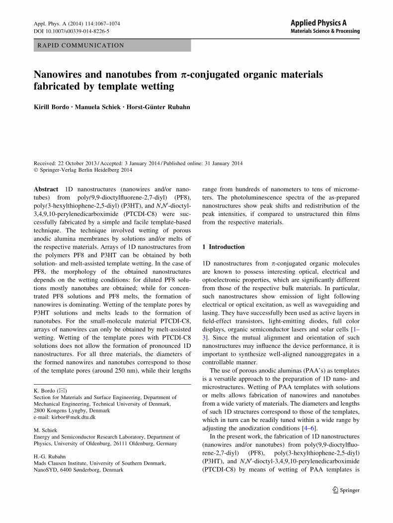
considered. The structural formulae of these compounds
are shown in Fig. 1.
The investigation of the formation of 1D nanostructures
from these materials is important, since they are promising
candidates for different electronic device applications. PF8
and other polyfluorenes are typical active materials in blue
light-emitting diodes [7, 8]. P3HT is widely used in BHJ
solar cells [9–11]. PTCDI and perylene-diimide derivatives
are employed in field-effect transistors and other electronic
devices [12–14].
Nanowires (or ‘‘nanohillocks’’) from P3HT were pre-
pared via solution-assisted [15, 16] or melt-assisted [9,
17, 18] wetting of PAA templates, and also by nano-
imprint lithography, using thin PAA films on Si sub-
strates as stamps [11, 19]. The fabrication of PF8
nanowires and nanotubes has also been reported [20–23].
Needle-like nanoaggregates from several different per-
ylene-diimide derivatives were obtained by self-assembly
from solutions [24, 25]. However, this technique only
allowed the formation of randomly oriented ‘‘nanonee-
dles’’ having different lengths and widths. In addition,
nanotube arrays from perylene were fabricated by solu-
tion-assisted template wetting [26] and pyridine-perylene-
diimide nanowires were made by electrophoretic depo-
sition into the pores of a PAA template [27]. In general,
facile and size-controlled preparation of well-defined
nanowires or nanotube arrays from these materials is still
a challenge.
In the present paper, we report on the fabrication of 1D
nanostructures from PF8, P3HT and PTCDI-C8. The
nanostructures were made in a controllable manner by
employing both solution- and melt-assisted wetting of PAA
templates. The solution-assisted wetting by PF8 and P3HT
was studied for two different concentrations of the pre-
cursor solutions. The effects of the preparation conditions
on the morphology of the obtained nanostructures, as well
as their optical properties, are discussed.
2 Experimental section
PF8 (regioregular, semiconductor grade, Sigma-Aldrich),
P3HT (regioregular, semiconductor grade, Rieke Metals)
and PTCDI-C8 (semiconductor grade, Sigma-Aldrich)
were used without further purification.
For the fabrication of nanostructures by means of tem-
plate wetting, mainly commercial membrane filters (Ano-
disc 25, Whatman Ltd.) were used. These membranes had
mean pore diameter of 200 nm and thickness of 60 lm
(according to the manufacturer’s data). The real pore
diameter was found to be 244 ± 48 nm previously [22].
In some of the experiments, lab-made thin-film PAA
templates were employed. Such templates were prepared
by the anodization of thin evaporated Al films on ITO-
coated glass substrates. A detailed description of this pro-
cedure can be found elsewhere [28]. Briefly, the Al films
(thickness 1 lm) were deposited by e-beam evaporation
from a 99.99 % pure Al target in a conventional PVD
machine (Edwards Auto 500). In order to improve the
adhesion of the Al to the substrate, a thin (2 nm) layer of Ti
was applied. The as-prepared thin Al films were anodized
in 0.3 M oxalic acid at 40 V, and the pores of the formed
PAA films were subsequently widened by etching in 5 %
phosphoric acid for 45 min. at room temperature. The
obtained templates had pore diameters of about 80 nm and
thickness of about 1.5 lm.
All three materials were introduced into the pores of the
templates by both solution- and melt-assisted wetting.
For the solution-assisted wetting, two solutions of PF8
in toluene and two solutions of P3HT in chlorobenzene
having different concentrations (a saturated solution and a
1 mg/ml solution for each material) were used. Because of
relatively low solubility of PTCDI-C8, only a saturated
solution of PTCDI-C8 in chloroform was employed. Sat-
urated solutions of the stated materials were prepared by
adding an excess amount of each material to a fixed volume
(about 1 ml) of the corresponding solvent in a glass vial
under constant stirring at room temperature. In the case of
PF8 and P3HT, a drop of a solution was placed on top of a
membrane and the membrane was sandwiched between
two glass slides. The membrane was left clamped between
the glass slides for about 10 h to allow slow evaporation of
the solvent. In the case of PTCDI-C8, the so-called ‘‘dip-
and-dry’’ method was employed. In that technique, the
porous membrane was dipped into the PTCDI-C8 solution
for 2 min. After dipping, the membrane was put on a 50 �C
Fig. 1 Structural formulae of
PF8 (a), P3HT (b) and PTCDI-
C8 (c)
1068 K. Bordo et al.
123
hot plate and the solvent was allowed to evaporate. In total,
20 ‘‘dip-and-dry’’ cycles were conducted.
For the melt-assisted wetting, thin films of PF8, P3HT
and PTCDI were formed on microscope glass slides by
drop-casting from the corresponding saturated solutions. A
porous membrane was placed on top of the film and cov-
ered by another glass slide. For each material, such a
‘‘sandwiched’’ structure was heated up slightly above the
respective melting point (to 180 �C for PF8, to 250 �C for
P3HT, to 340 �C for PTCDI-C8) for 15 min. The melting
was carried out on a hotplate placed in a glove box under
constant nitrogen flow. For the sake of comparison, some
of the mentioned drop-casted thin films were left as-pre-
pared, without template-assisted nanostructuring. These
films will be referred to as ‘‘non-structured’’ thin films.
Finally in all of the experiments a sticky carbon pad was
attached to one side of the membrane, while the other side
was cleaned from the excess polymer by scratching with a
scalpel. The nanowire/nanotube arrays were released by
dissolving the membrane in a 2 M NaOH solution.
Optical images of the obtained nanowire/nanotube
arrays were acquired by a fluorescence microscope equip-
ped with a high-pressure Hg lamp (Nikon Eclipse TE 300)
and a CCD camera. Photoluminescence spectra of the
nanostructures were measured on the same microscope
with a fiber spectrometer (Ocean Optics) attached. Scan-
ning electron microscopy (SEM) images of the nanowire/
nanotube arrays were collected using a Hitachi S-4800
instrument operating at beam voltages of 2–3 kV. In order
to facilitate SEM imaging, all the samples were coated with
Au/Pd (2 nm) by magnetron sputtering (Cressington HR
208 sputter coater).
3 Results and discussion
3.1 Morphology of the obtained nanostructures
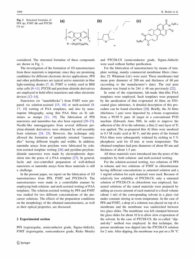
Fluorescence microscopy reveals arrays of bright blue-emit-
ting 1D nanostructures for PF8 and red-emitting structures for
P3HT and PTCDI-C8 (Fig. 2). It can be seen that the nano-
structures are merged together to form bundles. On the pre-
sented images, the tips of the nanostructures cannot be seen,
since their lengths are bigger than the depth of focus. The
magnification of the microscope is not sufficient to distinguish
between nanowires and nanotubes.
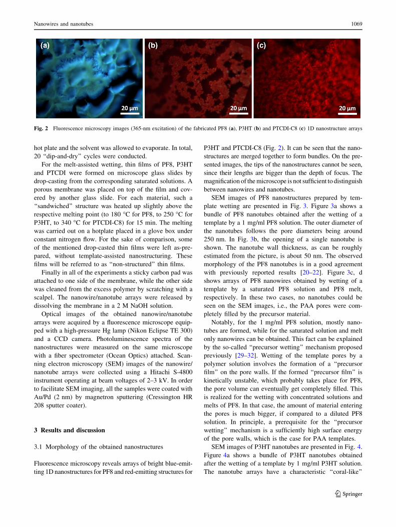
SEM images of PF8 nanostructures prepared by tem-
plate wetting are presented in Fig. 3. Figure 3a shows a
bundle of PF8 nanotubes obtained after the wetting of a
template by a 1 mg/ml PF8 solution. The outer diameter of
the nanotubes follows the pore diameters being around
250 nm. In Fig. 3b, the opening of a single nanotube is
shown. The nanotube wall thickness, as can be roughly
estimated from the picture, is about 50 nm. The observed
morphology of the PF8 nanotubes is in a good agreement
with previously reported results [20–22]. Figure 3c, d
shows arrays of PF8 nanowires obtained by wetting of a
template by a saturated PF8 solution and PF8 melt,
respectively. In these two cases, no nanotubes could be
seen on the SEM images, i.e., the PAA pores were com-
pletely filled by the precursor material.
Notably, for the 1 mg/ml PF8 solution, mostly nano-
tubes are formed, while for the saturated solution and melt
only nanowires can be obtained. This fact can be explained
by the so-called ‘‘precursor wetting’’ mechanism proposed
previously [29–32]. Wetting of the template pores by a
polymer solution involves the formation of a ‘‘precursor
film’’ on the pore walls. If the formed ‘‘precursor film’’ is
kinetically unstable, which probably takes place for PF8,
the pore volume can eventually get completely filled. This
is realized for the wetting with concentrated solutions and
melts of PF8. In that case, the amount of material entering
the pores is much bigger, if compared to a diluted PF8
solution. In principle, a prerequisite for the ‘‘precursor
wetting’’ mechanism is a sufficiently high surface energy
of the pore walls, which is the case for PAA templates.
SEM images of P3HT nanotubes are presented in Fig. 4.
Figure 4a shows a bundle of P3HT nanotubes obtained
after the wetting of a template by 1 mg/ml P3HT solution.
The nanotube arrays have a characteristic ‘‘coral-like’’
Fig. 2 Fluorescence microscopy images (365-nm excitation) of the fabricated PF8 (a), P3HT (b) and PTCDI-C8 (c) 1D nanostructure arrays
Nanowires and nanotubes 1069
123
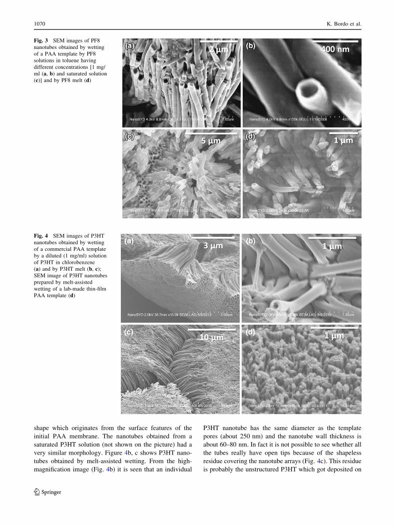
shape which originates from the surface features of the
initial PAA membrane. The nanotubes obtained from a
saturated P3HT solution (not shown on the picture) had a
very similar morphology. Figure 4b, c shows P3HT nano-
tubes obtained by melt-assisted wetting. From the high-
magnification image (Fig. 4b) it is seen that an individual
P3HT nanotube has the same diameter as the template
pores (about 250 nm) and the nanotube wall thickness is
about 60–80 nm. In fact it is not possible to see whether all
the tubes really have open tips because of the shapeless
residue covering the nanotube arrays (Fig. 4c). This residue
is probably the unstructured P3HT which got deposited on
Fig. 3 SEM images of PF8
nanotubes obtained by wetting
of a PAA template by PF8
solutions in toluene having
different concentrations [1 mg/
ml (a, b) and saturated solution
(c)] and by PF8 melt (d)
Fig. 4 SEM images of P3HT
nanotubes obtained by wetting
of a commercial PAA template
by a diluted (1 mg/ml) solution
of P3HT in chlorobenzene
(a) and by P3HT melt (b, c);
SEM image of P3HT nanotubes
prepared by melt-assisted
wetting of a lab-made thin-film
PAA template (d)
1070 K. Bordo et al.
123
the top of the PAA membrane during the wetting procedure
and could not be removed completely before the template
dissolution. On the other hand, open nanotube tips can be
clearly seen on the SEM image of a homemade supported
thin-film PAA template wetted by P3HT melt (Fig. 4d). In
that case, the excess of P3HT was completely removed
from the top of the template by carefully wiping it with a
toluene-soaked tissue. Here, the nanotube diameters cor-
respond to those of the thin-film template (60–80 nm) and
the nanotube wall thickness is about 20 nm.
It should be noted that for P3HT both solution- and
melt-assisted wetting lead to the preferential formation of
nanotubes, not nanowires. That can be explained by the
‘‘precursor wetting’’ mechanism which is described above
for PF8. However, in the case of P3HT the ‘‘precursor
film’’, which is formed on the walls of the PAA template, is
kinetically stable. The evaporation of the solvent (in the
case of P3HT solution) and solidification of the polymer
after cooling it below the melting point (in the case of
P3HT melt) leads to the formation of nanotubes in the
pores of the PAA template.
PTCDI-C8 was introduced into the template pores by
means of the so-called ‘‘dip-and-dry’’ method. SEM
imaging of the samples after complete removal of the PAA
did not reveal any pronounced nanostructures. At some
regions, only small PTCDI-C8 nanoaggregates could be
seen. Apparently, the employed number of ‘‘dip-and-dry’’
cycles was not enough to introduce sufficient amount of
material into the template pores and to allow the formation
of long 1D nanostructures. Another technique involved
melting of a PTCDI-C8 thin film formed on top of a PAA
template and filling the pores by the PTCDI-C8 melt, see
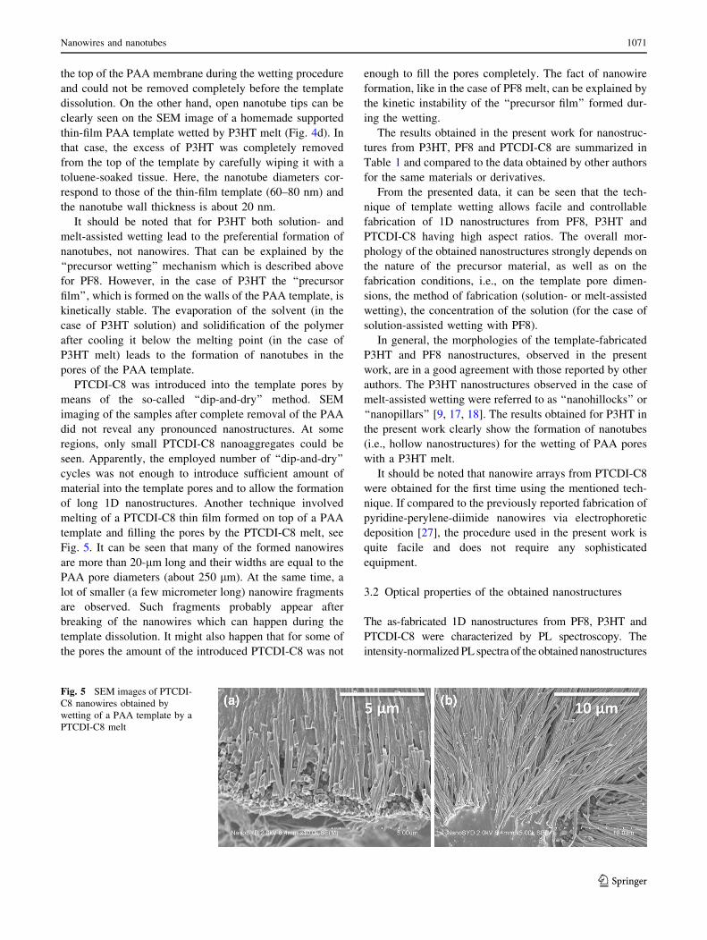
Fig. 5. It can be seen that many of the formed nanowires
are more than 20-lm long and their widths are equal to the
PAA pore diameters (about 250 lm). At the same time, a
lot of smaller (a few micrometer long) nanowire fragments
are observed. Such fragments probably appear after
breaking of the nanowires which can happen during the
template dissolution. It might also happen that for some of
the pores the amount of the introduced PTCDI-C8 was not
enough to fill the pores completely. The fact of nanowire
formation, like in the case of PF8 melt, can be explained by
the kinetic instability of the ‘‘precursor film’’ formed dur-
ing the wetting.
The results obtained in the present work for nanostruc-
tures from P3HT, PF8 and PTCDI-C8 are summarized in
Table 1 and compared to the data obtained by other authors
for the same materials or derivatives.
From the presented data, it can be seen that the tech-
nique of template wetting allows facile and controllable
fabrication of 1D nanostructures from PF8, P3HT and
PTCDI-C8 having high aspect ratios. The overall mor-
phology of the obtained nanostructures strongly depends on
the nature of the precursor material, as well as on the
fabrication conditions, i.e., on the template pore dimen-
sions, the method of fabrication (solution- or melt-assisted
wetting), the concentration of the solution (for the case of
solution-assisted wetting with PF8).
In general, the morphologies of the template-fabricated
P3HT and PF8 nanostructures, observed in the present
work, are in a good agreement with those reported by other
authors. The P3HT nanostructures observed in the case of
melt-assisted wetting were referred to as ‘‘nanohillocks’’ or
‘‘nanopillars’’ [9, 17, 18]. The results obtained for P3HT in
the present work clearly show the formation of nanotubes
(i.e., hollow nanostructures) for the wetting of PAA pores
with a P3HT melt.
It should be noted that nanowire arrays from PTCDI-C8
were obtained for the first time using the mentioned tech-
nique. If compared to the previously reported fabrication of
pyridine-perylene-diimide nanowires via electrophoretic
deposition [27], the procedure used in the present work is
quite facile and does not require any sophisticated
equipment.
3.2 Optical properties of the obtained nanostructures
The as-fabricated 1D nanostructures from PF8, P3HT and
PTCDI-C8 were characterized by PL spectroscopy. The
intensity-normalized PL spectra of the obtained nanostructures
Fig. 5 SEM images of PTCDI-
C8 nanowires obtained by
wetting of a PAA template by a
PTCDI-C8 melt
Nanowires and nanotubes 1071
123
as well as the respective ‘‘non-structured’’ thin films are pre-
sented in Fig. 6.
In the PL spectra of the ‘‘non-structured’’ thin films
before and after heat treatment, no changes were observed.
Therefore, it was assumed that the employed heat treatment
did not cause any change in the chemical composition of
the studied materials.
For the determination of the peak positions, each spec-
trum was fit with a set of Gaussian curves. The spectrum of
a spin-coated PF8 film (Fig. 6a) exhibits a vibronic pro-
gression with peaks at 441, 465 and 501 nm, corresponding
to 0–0, 0–1 and 0–2 vibronic transitions, respectively. A
broad peak at around 540 nm can also be seen. The PL
spectra of the PF8 nanotubes and nanowires are slightly
shifted to the blue with respect to that of PF8 thin film. The
broad featureless band centered around 540 nm can be
attributed to the on-chain chemical defects probably
associated with oxidatively generated fluorenone units [7,
8, 33–36]. The relative intensity of this band is maximal for
the PF8 nanowires, being significantly lower for the PF8
nanotubes and the thin film.
It can be seen that the relative intensities of the 0–0 and
0–1 vibronic peaks are significantly changed for the PF8
nanowires and nanotubes, compared to PF8 thin film. In
particular, the relative intensity of the 0–0 peak decreases
for the PF8 nanowires and increases for the PF8 nanotubes.
The relative intensity of the 0–1 peak exhibits the opposite
trend. It should be noted, however, that PF8 nanostructures
of both morphologies (nanowires and nanotubes) can be
present on the observed areas of the samples simulta-
neously. Thus, the observed PL spectra might be a super-
position of the spectra for both nanowires and nanotubes.
Therefore, it is difficult to attribute the observed spectral
features to any particular form of PF8 nanostructures.
Table 1 1D nanostructures from PF8, P3HT and perylene derivatives fabricated via template-based techniques
Material Reference Method of
fabrication
Fabrication conditions Morphology of the
nanostructures
Length/outer diameter of
the nanostructures
P3HT [15] SAW 2 mg/ml P3HT in chloroform Nanotubes 200/65 nm
[16] SAW 0.5 % P3HT in chloroform Nanotubes 100-nm outer diameter
[9] MAW 250 �C, 30 min., in air Nanopillars 295/269 nm
[17] MAW 250 �C, 30 min., in air Nanopillars 500/52 nm
[18] MAW 250 �C, vacuum Nanohillocks 800/100 nm
[11] NIL 230 �C, 10 min., vacuum Nanopillars 200/50 nm
[19] NIL with PAA film
on Si as a stamp
125 �C Nanohillocks 450/80 nm
Present
work
SAW 1 mg/ml P3HT in chlorobenzene Nanotubes Tens of lm/250 nm
Present
work
SAW Saturated solution of P3HT in
chlorobenzene
Nanotubes Tens of lm/250 nm
MAW 250 �C, 15 min., N2 flow Nanotubes Tens of lm/250 nm
MAW 250 �C, 15 min., N2 flow Nanotubes 1.5 lm/60–80 nm
PF8 [20] SAW 60 mg/ml PF8 in THF Nanowires Not stated
[21] SAW 60 mg/ml PF8 in THF Nanowires 46 lm/232 nm
[22] SAW 40 mg/ml PF8 in THF Nanotubes Diameter: 257 nm
[23] MAW 250 �C, 2 h, vacuum Nanowires Not stated
Present
work
SAW 1 mg/ml PF8 in THF Nanotubes Tens of lm/250 nm
SAW Saturated solution of PF8 in THF Nanowires Tens of lm/250 nm
MAW 180 �C, 15 min., N2 flow Nanowires Tens of lm/250 nm
Perylene [26] MAW 240 �C 10 h, N2 flow Nanotubes 60 lm/200 nm
Pyridine-perylene-
diimide
[27] ED into PAA
template
CF3COOH as protonating agent Nanowires 20 lm/80 nm
Other perylene-
diimide
derivatives
[24, 25] Self-assembly from
solutions
– Nanowires or
‘‘nanoneedles’’
Up to 500 lm/ca.
200 nm
PTCDI-C8 Present
work
SAW Saturated solution of PTCDI-C8 in
chloroform, ‘‘drip-and-dry’’
None Hundreds of nm
MAW 340 �C, 15 min., N2 flow Nanowires Tens of lm/250 nm
MAW melt-assisted wetting, SAW solution-assisted wetting, NIL nanoimprint lithography, ED electrophoretic deposition
1072 K. Bordo et al.
123

The fitting of the PL spectrum of a thin spin-coated
P3HT film (Fig. 6b) reveals three peaks at 650, 730 and
810 nm. The spectrum of P3HT nanotubes is blue-shifted
with respect to the spectrum of the P3HT thin film. Like in
the case of PF8, a redistribution of peak intensities is
observed. The relative intensity of the 0–0 peak decreases
for the P3HT nanotubes, while the relative intensity of the
0–1 peak increases.
The PL spectrum of a drop-casted PTCDI-C8 film
(Fig. 6c) shows the main peak at 680 nm and a shoulder at
around 640 nm. In the spectrum of PTCDI-C8 nanowires,
the main peak is red-shifted compared to that of the thin
film and an additional shoulder appears at around 800 nm.
Peak shifts and redistribution of peak intensities in PL
spectra have been observed previously for 1D nanostruc-
tures from different p-conjugated organic materials [20–22,
37–43].
For the polymers, PF8 and P3HT, such spectral features
can be explained by phase transitions or changes in the
molecular alignment occurring during the template pore
filling. In particular, the presence of large amount of b-
phase was shown for PF8 nanowires prepared by solution-
assisted wetting [20–22]. The observed phase transition
was attributed to the mechanical stresses arising within a
polymer material during the pore filling and solvent
evaporation.
In general, the observed changes in the PL spectra can
also be explained by surface effects associated with 1D
nanostructures [37, 42]. In nanowires and nanotubes, the
fraction of molecules existing on the surface of these
nanostructures is significantly higher than in the respective
bulk materials or drop-casted thin films. The energy states
and energetic coupling of these molecules are different
when compared to those located in the bulk. That leads to
the changes in the overall structure of absorption and
emission spectra observed for the nanowires and
nanotubes.
In order to determine the particular mechanisms
responsible for the observed spectral changes, more
detailed spectroscopic studies (including, e.g., temperature-
dependent photoluminescence and polarization measure-
ments) are required.
4 Conclusions
In the present work, facile and controllable template-based
fabrication of 1D nanostructures from PF8, P3HT and
PTCDI-C8 is reported. Nanostructures from the polymers
P3HT and PF8 can be obtained by both solution- and melt-
assisted template wetting. For these materials, the so-called
‘‘precursor wetting’’ is realized. For P3HT, the ‘‘precursor
film’’ formed on the pore walls is kinetically stable, and
therefore this material can only form nanotubes––for wet-
ting with both solutions and melts. For PF8, the formed
‘‘precursor film’’ is not stable and the morphology of the
obtained nanostructures depends on the amount of material
introduced into the pores. For solutions with lower
Fig. 6 Intensity-normalized photoluminescence spectra of the fab-
ricated nanostructures and the respective ‘‘non-structured’’ thin films:
PF8 (a), P3HT (b) and PTCDI-C8 (c)
Nanowires and nanotubes 1073
123
concentrations, mostly nanotubes are obtained. For highly
concentrated solutions and melts, the pore volume can be
filled completely, and the formation of nanowires is dom-
inating. The small-molecule material PTCDI-C8 can be
introduced into a PAA template by wetting it with a melt.
Even a big number of ‘‘dip-and-dry’’ cycles in solution-
assisted wetting do not allow the formation of pronounced
1D nanostructures.
The photoluminescence spectra of the as-prepared
nanostructures show peak shifts and redistribution of the
peak intensities, compared to unstructured thin films from
the respective materials.
As can be seen from the obtained results, the method of
template wetting provides an effective and reliable general
route for the preparation of 1D nanostructures from prac-
tically important organic polymers and small molecules.
The fabrication of supported PF8, P3HT and PTCDI-C8
nanowire and/or nanotube arrays by wetting of thin-film
PAA templates would be the next step in the realization of
highly efficient electronic devices based on these materials.
Acknowledgments The authors are grateful to the Danish research
agency as well as the Danish Advanced Technologies Trust for sup-
porting this work by various grants.
References
1. F.S. Kim, G. Ren, S.A. Jenekhe, Chem. Mater. 23, 682 (2011)
2. S.B. Jo, W.H. Lee, L. Qiu, K. Cho, J. Mater. Chem. 22, 4244
(2012)
3. A.L. Briseno, S.C.B. Mannsfeld, S.A. Jenekhe, Z. Bao, Y.N. Xia,
Mater. Today 11, 38 (2008)
4. C.R. Martin, Chem. Mater. 8, 1739 (1996)
5. G. Cao, D. Liu, Adv. Coll. Interf. Sci. 136, 45 (2008)
6. R.O. Al-Kaysi, T.H. Ghaddar, G. Guirado, J. Nanomat. 2009, 1
(2009)
7. J.M. Lupton, J. Klein, Synth. Met. 138, 233 (2003)
8. W. Zhao, T. Cao, J.M. White, Adv. Funct. Mater. 14, 783 (2004)
9. A. Santos, P. Formentin, J. Pallares, J. Ferre-Borrull, L.F. Marsal,
Sol. Energ. Mat. Sol. C. 94, 1247 (2010)
10. M.T. Dang, L. Hirsch, G. Wantz, Adv. Mater. 23, 3597 (2011)
11. D. Chen, W. Zhao, T.P. Russell, ACS Nano 6, 1479 (2012)
12. A.L. Briseno, S.C.B. Mannsfeld, C. Reese, J.M. Hancock, Y.
Xiong, S.A. Jenekhe, Z. Bao, Y. Xia, Nano Lett. 7, 2847 (2007)
13. J.H. Oh, H.W. Lee, S. Mannsfeld, R.M. Stoltenberg, E. Jung,
Y.W. Jin, J.M. Kim, J.-B. Yoo, Z. Bao, PNAS 106, 6065 (2009)
14. H. Yu, Z. Bao, J.H. Oh, Adv. Funct. Mater. 23, 629 (2013)
15. J.P. Cannon, S.D. Bearden, S.A. Gold, Compos. A 41, 836 (2010)
16. J. Byun, Y. Kim, G. Jeon, J.K. Kim, Macromolecules 44, 8558
(2011)
17. A. Santos, P. Formentin, J. Pallares, J. Ferre-Borrull, L.F. Marsal,
Mat. Lett. 64, 371 (2010)
18. J.S. Kim, Y. Park, D.Y. Lee, J.H. Lee, J.H. Park, J.K. Kim, K.
Cho, Adv. Funct. Mater. 20, 540 (2010)
19. W. Wiedermann, L. Sims, A. Abdelilah, A. Exner, R. Meier, K.P.
Musselman, J.L. MacManus-Driscoll, P. Muller-Buschbaum, G.
Scarpa, P. Lugli, L. Schmidt-Mende, Appl. Phys. Lett. 96,
263109 (2010)
20. D. O’Carrol, G. Redmond, Chem. Mater. 20, 6501 (2008)
21. D. O’Carrol, D. Iacopino, A. O’Riordan, P. Lovera, E. O’Connor,
G.A. O’Brien, G. Redmond, Adv. Mater. 20, 42 (2008)
22. S. Moynihan, D. Iacopino, D. O’Carrol, P. Lovera, G. Redmond,
Chem. Mater. 20, 996 (2008)
23. D. O’Carrol, I. Lieberwirth, G. Redmond, Small 3, 1178 (2007)
24. Y. Che, A. Datar, K. Balakrishnan, L. Zang, J. Am. Chem. Soc.
129, 7234 (2007)
25. Y. Che, X. Yang, K. Balakrishnan, J. Zuo, L. Zang, Chem. Mater.
21, 2930 (2009)
26. L. Zhao, W. Yang, Y. Ma, J. Yao, Y. Li, H. Liu, Chem. Commun.
19, 2442 (2003)
27. R. Bai, M. Ouyang, R.-J. Zhou, M.-M. Shi, M. Wang, H.-Z.
Chen, Nanotechnology 19, 1 (2008)
28. K. Bordo, Nanoporous thin film templates for the fabrication of
nanowires and nanotubes (Ph.D. thesis, University of Southern
Denmark, Sønderborg, 2011)
29. http://www.mpi-halle.mpg.de. Accessed 16 Dec 2012
30. M. Steinhart, R.B. Wehrspohn, U. Gosele, J.H. Wendorff, An-
gew. Chem. Int. Ed. 43, 1334 (2004)
31. M. Steinhart, J.H. Wendorff, A. Greiner, R.B. Wehrspohn, K.
Nielsch, J. Schilling, J. Choi, U. Gosele, Science 296, 1997
(2002)
32. S. Schlitt, A. Greiner, J.H. Wendorff, Macromolecules 41, 3228
(2008)
33. A.C. Grimsdale, K.L. Chan, R.E. Martin, P.G. Jokisz, A.B.
Holmes, Chem. Rev. 109, 897 (2009)
34. A.C. Grimsdale, K. Mullen, Adv. Polym. Sci. 199, 1 (2006)
35. A.C. Grimsdale, K. Mullen, Macromol. Rapid Commun. 28, 1676
(2007)
36. A.C. Grimsdale, K. Mullen, Adv. Polym. Sci. 212, 1 (2008)
37. J.-K. Lee, W.-K. Koh, W.-S. Chae, Y.-R. Kim, Chem. Commun.
2, 138 (2002)
38. S. Guha, J.D. Rice, Y.T. Yau, C.M. Martin, M. Chandrasekhar,
H.R. Chandrasekhar, R. Guentner, P. Scanduicci de Freitas, U.
Scherf, Phys. Rev. B 67, 125204 (2003)
39. J. Beermann, S.I. Bozhevolnyi, V.G. Bordo, H.-G. Rubahn, Opt.
Commun. 237, 423 (2004)
40. J. Beermann, S.I. Bozhevolnyi, F. Balzer, H.-G. Rubahn, Laser
Phys. Lett. 2, 480 (2005)
41. F. Balzer, A. Pogantsch, H.-G. Rubahn, J. Lumin. 129, 784
(2009)
42. X.-P. Shen, G. Yin, C. Gao, Z. Xu, Mat. Chem. Phys. 113, 202
(2009)
43. K. Bordo, M. Schiek, A. Ghazal, I. Wallmann, A. Lutzen, F.
Balzer, H.-G. Rubahn, J. Phys. Chem. C 115, 20882 (2011)
1074 K. Bordo et al.
123
Related Documents


![Nanoparticle-doped electrospun fiber random lasers with ... · [2,6,8,10]. Organic crystals [16,17] and epitaxial nanowires [18], biopolymers [19,20], as well as conjugated polymers](https://static.cupdf.com/doc/110x72/600d3d88f8e5ef616721ea08/nanoparticle-doped-electrospun-fiber-random-lasers-with-26810-organic.jpg)
