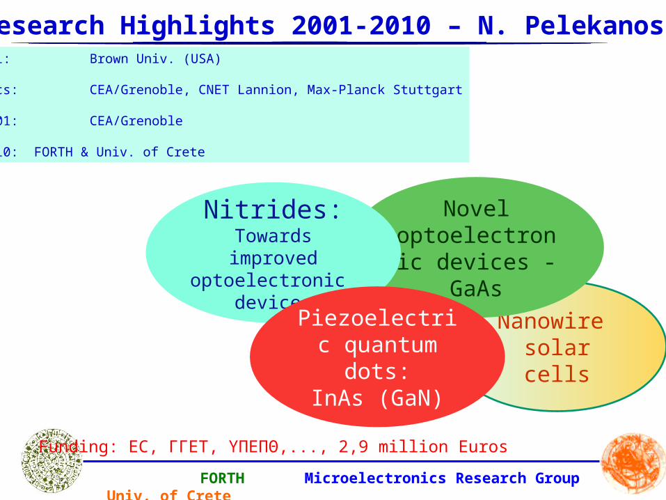
Nanowire solar cells Novel optoelectron ic devices - GaAs esearch Highlights 2001-2010 – N. Pelekanos Nitrides: Towards improved optoelectronic devices Piezoelectri c quantum dots: InAs (GaN) Funding: EC, ΓΓΕΤ, ΥΠΕΠΘ,..., 2,9 million Euros FORTH Microelectronics Research Group Univ. of Crete 1: Brown Univ. (USA) cs: CEA/Grenoble, CNET Lannion, Max-Planck Stuttgart 01: CEA/Grenoble 10: FORTH & Univ. of Crete

Welcome message from author
This document is posted to help you gain knowledge. Please leave a comment to let me know what you think about it! Share it to your friends and learn new things together.
Transcript
Nanowire solar cells
Novel optoelectronic
devices - GaAs
Research Highlights 2001-2010 – N. Pelekanos
Nitrides:Towards improved
optoelectronic devices
Piezoelectric quantum dots:
InAs (GaN)
Funding: EC, ΓΓΕΤ, ΥΠΕΠΘ,..., 2,9 million Euros
FORTH Microelectronics Research Group Univ. of Crete
PhD 1991: Brown Univ. (USA)
Post-docs: CEA/Grenoble, CNET Lannion, Max-Planck Stuttgart
1994-2001: CEA/Grenoble
2001-2010: FORTH & Univ. of Crete
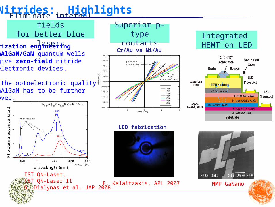
Eliminate internal fieldsfor better blue lasers
Superior p-type contacts Integrated
HEMT on LED
Nitrides: Highlights
IST QN-Laser,IST QN-Laser IIG. Dialynas et al. JAP 2008
-4 -2 0 2 4-0.025
-0.020
-0.015
-0.010
-0.005
0.000
0.005
0.010
0.015
0.020
0.025
Ni/Au
RTA @500oC in air
10 m 18 m 26 m 34 m 42 m 50 m 58 m
curr
en
t (A
)
votage (V)
p-GaN/A/Bas-deposited
Cr/Au vs Ni/Au
F. Kalaitzakis, APL 2007
LED fabrication
NMP GaNano
Polarization engineering on InAlGaN/GaN quantum wells can give zero-field nitride optoelectronic devices.
But, the optoelectronic quality of InAlGaN has to be further improved.
360 380 400 420 440
#347
#346
4nm
In0.14
Al0.25
Ga0.61
N/GaN QWs
8nm
GaN-related
Pho
tolu
min
esce
nce
(a.u
.)
Wavelength (nm)325nm, 17K
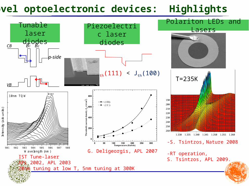
Polariton LEDs and LasersPiezoelectric laser diodes
Tunable laser diodes
Novel optoelectronic devices: Highlights
Jth(111) < Jth(100)
G. Deligeorgis, APL 2007 901 902 903 904 905 906 907 908
laser10nm TQW
Inte
nsity
(ar
b.un
its)
Wavelength (nm)
p-side
CB B1 B2
VB
IST Tune-laser APL 2002, APL 200320nm tuning at low T, 5nm tuning at 300K
190
200
210
220
230
240
250
260
1.3601.3551.3501.3451.3401.3351.330
-S. Tsintzos, Nature 2008
-RT operation, S. Tsintzos, APL 2009.
T=235K
VV
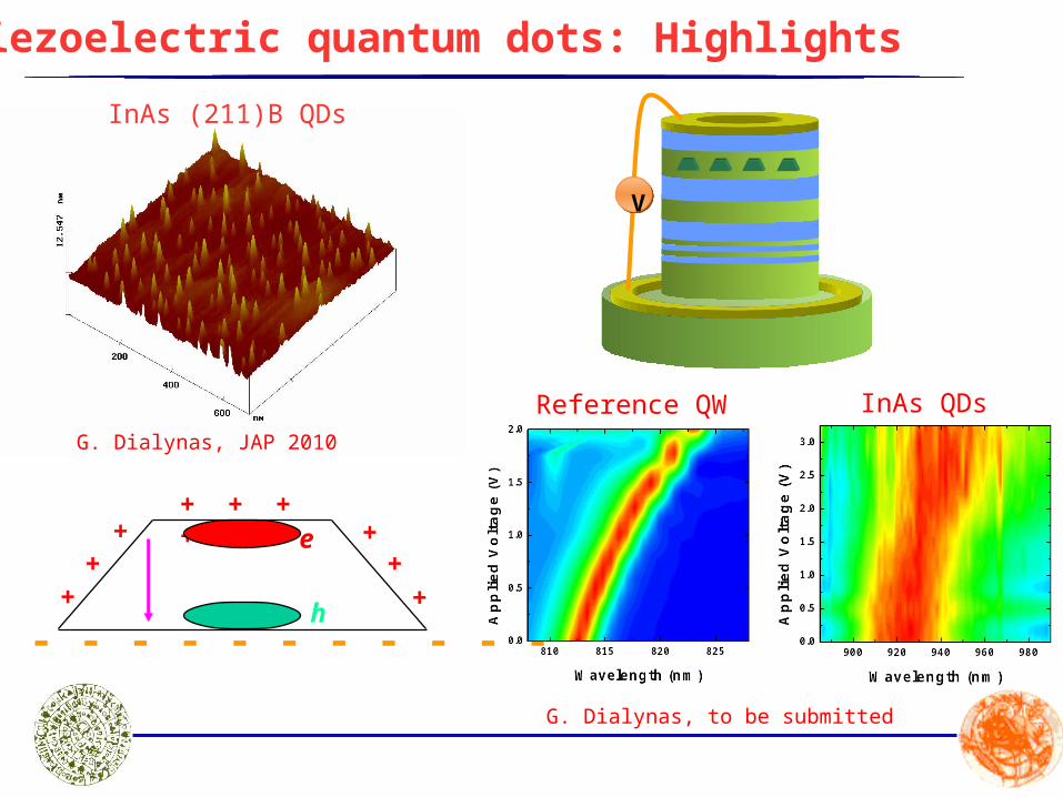
Piezoelectric quantum dots: Highlights
+ + + + +
- - - - - - - - - - - - -
+
+
+
+++
e
h
InAs (211)B QDs
G. Dialynas, JAP 2010
G. Dialynas, to be submitted
Reference QW InAs QDs
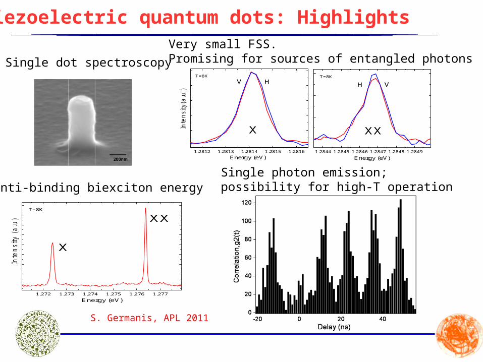
1.2812 1.2813 1.2814 1.2815 1.2816Energy (eV)
T=8KV H
XInte
nsity
(a.u
.)
1.2844 1.2845 1.2846 1.2847 1.2848 1.2849
Energy (eV)
T=8K
XX
VH
Very small FSS. Promising for sources of entangled photons
Single photon emission; possibility for high-T operationAnti-binding biexciton energy
1.272 1.273 1.274 1.275 1.276 1.277
T=8K
XX
X
Inte
nsity (a.u
)
Energy (eV)
Single dot spectroscopy
Piezoelectric quantum dots: Highlights
S. Germanis, APL 2011
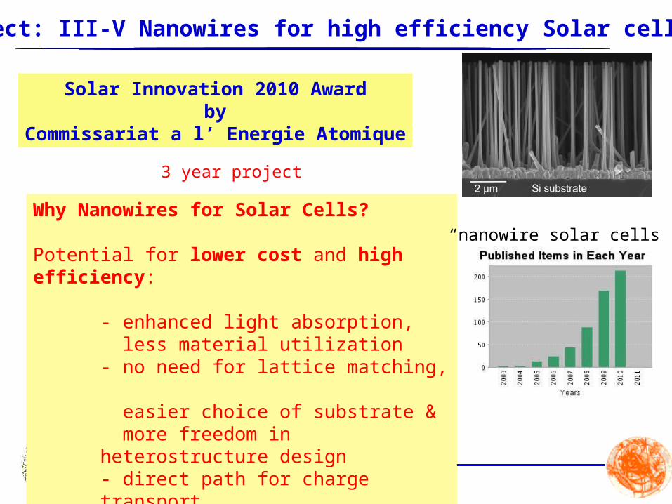
Project: III-V Nanowires for high efficiency Solar cells
Solar Innovation 2010 Awardby
Commissariat a l’ Energie Atomique
Why Nanowires for Solar Cells?
Potential for lower cost and high efficiency:
- enhanced light absorption, less material utilization- no need for lattice matching, easier choice of substrate & more freedom in heterostructure design- direct path for charge transport
“nanowire solar cells”
3 year project
Related Documents