Nanostructures and Nanostructuring Why Nanostructures ? Note: Nanostructures not equal to Nanomaterials, albeit common concepts Examples: ‘Devices’: Transistors, Processors, D-RAM, …. ‘Functional Surfaces’ www.psi.ch/lmn www.empa.ch Visions towards the Future: Self-organisation providing functional structures of higher and higher complexity

Welcome message from author
This document is posted to help you gain knowledge. Please leave a comment to let me know what you think about it! Share it to your friends and learn new things together.
Transcript
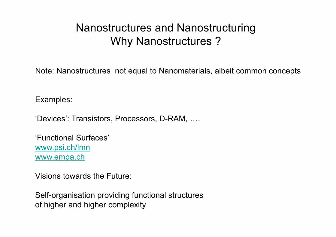
Nanostructures and NanostructuringWhy Nanostructures ?
Note: Nanostructures not equal to Nanomaterials, albeit common concepts
Examples:
‘Devices’: Transistors, Processors, D-RAM, ….
‘Functional Surfaces’www.psi.ch/lmnwww.empa.ch
Visions towards the Future:
Self-organisation providing functional structures of higher and higher complexity

Nanostructures and Nanostructuring
Bildungs- und Wachstumsmechanismen � 20.09.11 27.09.11 Selbst-Organisation 04.10.11 Analyse: Rastertunnel- und Rasterkraft-Mikroskopie, SEM, TEM 11.10.11 Analyse: Ellipsometrie Photoemissionsspektroskopie 18.10.11 Verdampfung, PVD, MBE, Nano-Cluster 25.10.11 Sputtering Ionenstrahl Sputtering, Magnetron Sputtering 01.11.11 Chemical Vapor deposition (CVD) 08.11.11 Lithographie und Ätzprozesse 15.11.11 Ionen-Implantation 22.11.11 Kolloidale Methoden und inverse Mizellen 29.11.11 Nanostrukturen 06.12.11 Laborführung 13.12.11 Prüfung 20.12.11
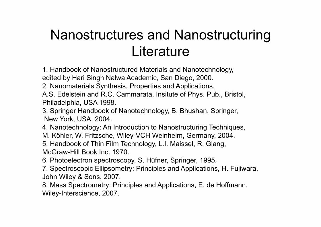
Nanostructures and NanostructuringLiterature
1. Handbook of Nanostructured Materials and Nanotechnology, edited by Hari Singh Nalwa Academic, San Diego, 2000. 2. Nanomaterials Synthesis, Properties and Applications, A.S. Edelstein and R.C. Cammarata, Insitute of Phys. Pub., Bristol, Philadelphia, USA 1998. 3. Springer Handbook of Nanotechnology, B. Bhushan, Springer,New York, USA, 2004. 4. Nanotechnology: An Introduction to Nanostructuring Techniques, M. Köhler, W. Fritzsche, Wiley-VCH Weinheim, Germany, 2004. 5. Handbook of Thin Film Technology, L.I. Maissel, R. Glang, McGraw-Hill Book Inc. 1970. 6. Photoelectron spectroscopy, S. Hüfner, Springer, 1995. 7. Spectroscopic Ellipsometry: Principles and Applications, H. Fujiwara, John Wiley & Sons, 2007. 8. Mass Spectrometry: Principles and Applications, E. de Hoffmann, Wiley-Interscience, 2007.

Nanostruktures: Important conceptsDimensionality ‘dot’ vs ‘wire’ vs sheetRatio Bulk I vs Bulk II ‘matrix & filler’, ceramicControlling by size effects ‘optic’, ‘electronic’ etc.Controlling by anisotropy ‘polymer – polarizer’Controlling contact area ‘lotus effect’Controlling by proximity @ Interface ‘field effect transistor’Sub-wavelength optics (diffraction) ‘~ photons, ~ 1...
Important: Nanostructuring: Mostly 2D or pseudo 3D3D: wishful thinking but enormous potential
( ‘brain’ vs ‘processor’ )
Crucial: Control ‘Surface / Interface active components’ need very clean materials (~d3) / surfaces (d2)
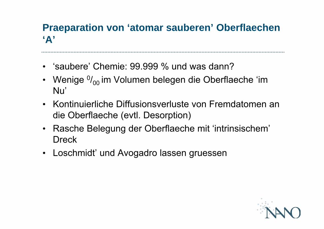
Praeparation von ‘atomar sauberen’ Oberflaechen ‘A’
• ‘saubere’ Chemie: 99.999 % und was dann?• Wenige 0/00 im Volumen belegen die Oberflaeche ‘im
Nu’• Kontinuierliche Diffusionsverluste von Fremdatomen an
die Oberflaeche (evtl. Desorption)• Rasche Belegung der Oberflaeche mit ‘intrinsischem’
Dreck• Loschmidt’ und Avogadro lassen gruessen

Praeparation von ‘atomar sauberen’ Oberflaechen ‘B’
• Oberflaechenbelegungsdichte nach Exposition eines Gases:
1 Langmuir ~ 10-6 mbar sec• Fuer Experimentierdauern von einem Tag (typisch!)
braucht es <~ 10-10 mbar • UHV !
N.B. nur wenige Oberflaechen, HOPG, Glimmer, ITO sind so inert, dass sie nach Luftexposition ohne Praeparation im Vakuum verwendet werden koennen.
Roland SteinerSept. 200911:49
7
Roland SteinerSept. 200911:49
8
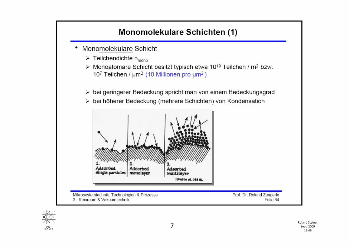
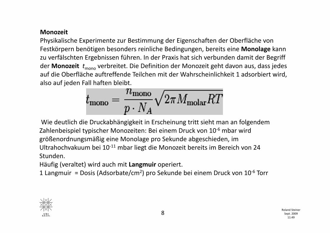
MonozeitPhysikalische Experimente zur Bestimmung der Eigenschaften der Oberfläche von Festkörpern benötigen besonders reinliche Bedingungen, bereits eine Monolage kann zu verfälschten Ergebnissen führen. In der Praxis hat sich verbunden damit der Begriff der Monozeit tmono verbreitet. Die Definition der Monozeit geht davon aus, dass jedes auf die Oberfläche auftreffende Teilchen mit der Wahrscheinlichkeit 1 adsorbiert wird, also auf jeden Fall haften bleibt.
Wie deutlich die Druckabhängigkeit in Erscheinung tritt sieht man an folgendem Zahlenbeispiel typischer Monozeiten: Bei einem Druck von 10‐6 mbar wird größenordnungsmäßig eine Monolage pro Sekunde abgeschieden, im Ultrahochvakuum bei 10‐11 mbar liegt die Monozeit bereits im Bereich von 24 Stunden.Häufig (veraltet) wird auch mit Langmuir operiert. 1 Langmuir = Dosis (Adsorbate/cm2) pro Sekunde bei einem Druck von 10‐6 Torr
Roland SteinerSept. 200911:49
9
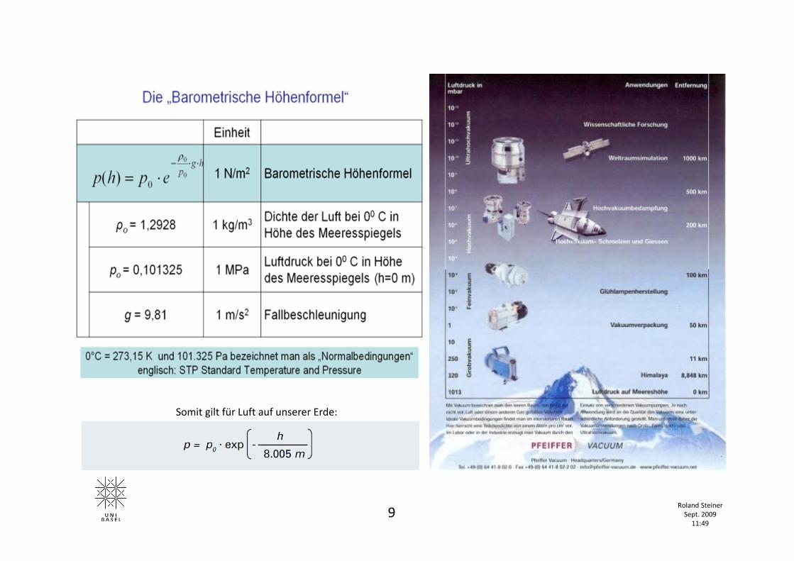
Somit gilt für Luft auf unserer Erde:
Technologie und Innovation
• Ist ein wesentlicher Vorteil fuer eine Gesellschaft• Ist von kommerziellem Interesse / vertraulich• Kommt aus der ‘offenen’ Wissenschaft heraus, nur selten durch die
Wissenschaftler selber• Wird durch Patente und Marken geschuetzt• Vakuumtechnik, Oberflaechenanalytik und Oberflaechenchemie /
Physik haben eine gemeinsame Entwicklung erfahren seit ~40 Jahren
Nanostructures and Nanostructuring20. / 27. Sept 2011
• Bildungs- und Wachstumsmechanismen • Oberflächendiffusion • Wachstumsmoden (ballistisch, dendritisch) • Oberflächendiffusion • amorph, poly, einkristallin • Epitaxie
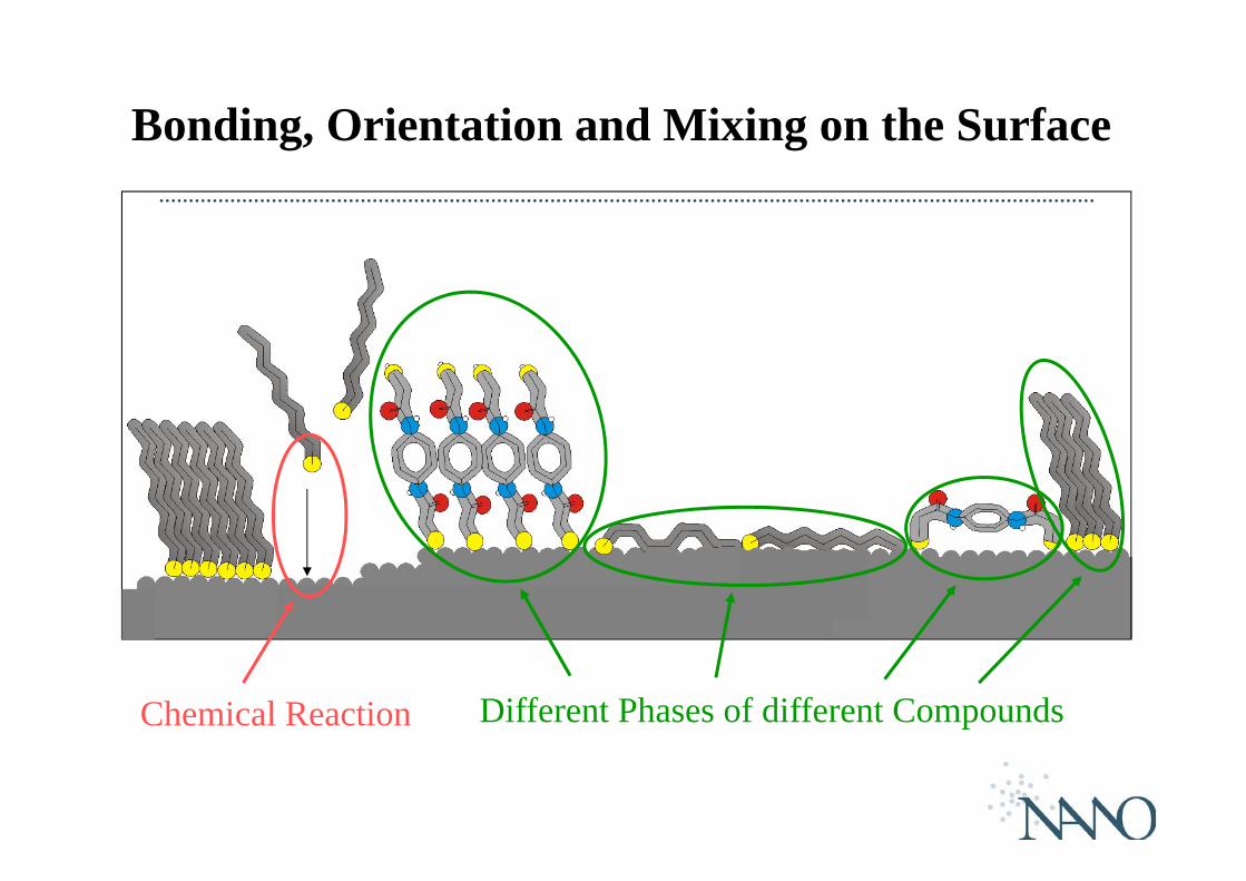
Bonding, Orientation and Mixing on the Surface
Au(111) surface
Chemical Reaction Different Phases of different Compounds
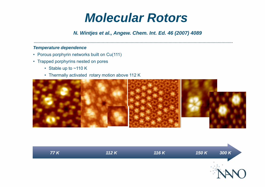
77 K 112 K 116 K 150 K 300 K
Temperature dependence• Porous porphyrin networks built on Cu(111)• Trapped porphyrins nested on pores
• Stable up to ~110 K• Thermally activated rotary motion above 112 K
Molecular RotorsN. Wintjes et al., Angew. Chem. Int. Ed. 46 (2007) 4089
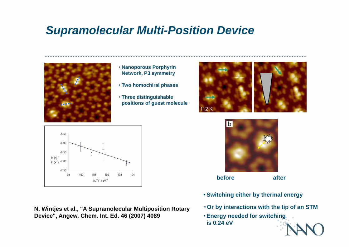
Supramolecular Multi-Position Device
before after
• Switching either by thermal energy
• Nanoporous PorphyrinNetwork, P3 symmetry
• Two homochiral phases
• Three distinguishablepositions of guest molecule
• Or by interactions with the tip of an STM
-7.50
-7.00
-6.50
-6.00
-5.50
99 100 101 102 103 104
(kBT)-1 / eV -1
ln (h) / ln (s-1)
• Energy needed for switchingis 0.24 eV
112 K
N. Wintjes et al., "A Supramolecular Multiposition Rotary Device", Angew. Chem. Int. Ed. 46 (2007) 4089

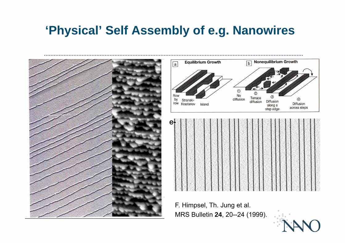
‘Physical’ Self Assembly of e.g. Nanowires
F. Himpsel, Th. Jung et al. MRS Bulletin 24, 20--24 (1999).
e-e-e-
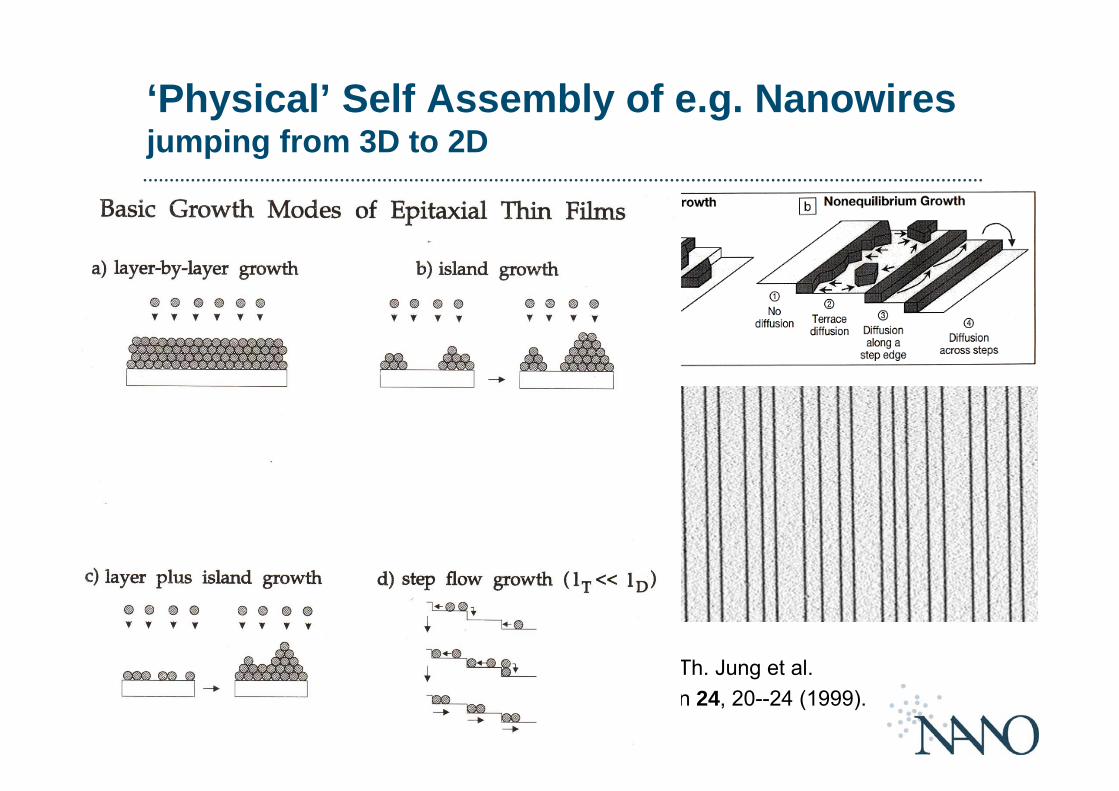
‘Physical’ Self Assembly of e.g. Nanowiresjumping from 3D to 2D
F. Himpsel, Th. Jung et al. MRS Bulletin 24, 20--24 (1999).
e-e-e-

‘Physical’ Self Assembly of e.g. Nanowires
F. Himpsel, Th. Jung et al. MRS Bulletin 24, 20--24 (1999).
e-e-e-
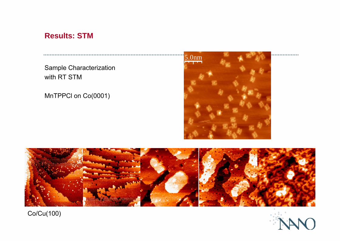
Results: STM
Sample Characterizationwith RT STM
MnTPPCl on Co(0001)
Co/Cu(100)
5.0nm
Praeparation von ‘atomar sauberen’ Oberflaechen oder ‘Grenzflaechen’
• Heizen (Si-1200, Pt-1200, W-2400, Mo-2400, Cu-500, …) bei kontaminationen auch mit reaktiven Gasen
• Zyklisches ‘annealing’ (dt. Ausheilen) und ‘sputtern’ (dt. Ionenbeschuss). Reinigen einer oberflaechennahen Schicht
• Aufdampfen ( ‘aufbringen’ im allgemeinsten Sinne) im Vakuum
Was passiert beim Aufbringen von Atomen oder Molekuelenauf Oberflaechen genau
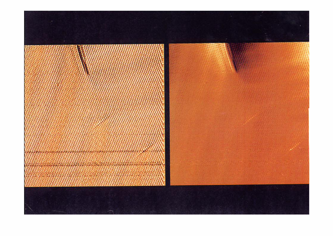
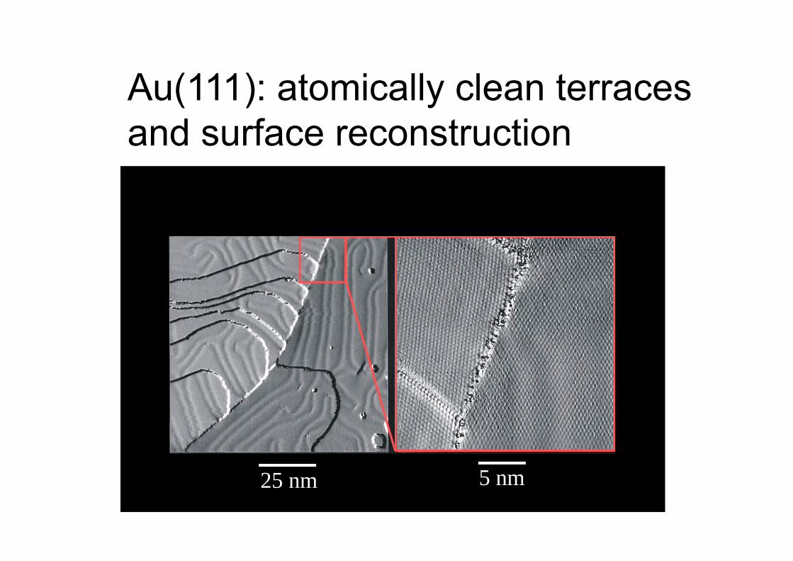
Au(111): atomically clean terracesand surface reconstruction
25 nm 5 nm
Related Documents


![Nanostructuring of Silicon Surface with Femtosecond ... · Nanostructuring of Silicon Surface with Femtosecond - Laser-Induced Near-field . ... Uji, Kyoto 611-0011, ... [2,3,15-19],](https://static.cupdf.com/doc/110x72/5af5bb3a7f8b9a4d4d8f7a06/nanostructuring-of-silicon-surface-with-femtosecond-of-silicon-surface-with.jpg)