Proceedings of the International Workshop "Advanced Techniques for Energy Sources Investigation and Testing" 4 – 9 Sept. 2004, Sofia, Bulgaria NANOSTRUCTURED PEROVSKITE CONDUCTORS FOR SOFC AND ELECTROCHEMICAL DEVICES M. Viviani 1* , A. Barbucci 2 , M.T. Buscaglia 1 , V. Buscaglia 1 , P. Carpanese 2 , A. Testino 2 , R.V. Calderone 2 , L. Mitoseriu 2 , P. Nanni 2 , D. Vladikova 3 1 IENI - CNR, Via De Marini 6, 16149 Genova, Italy 2 DICheP, University of Genoa, P.le Kennedy, 1 16129 Genova, Italy 3 IEES – BAS, 10 Acad. G. Bonchev, 1113 Sofia, Bulgaria * Corresponding author: [email protected] Abstract Transport properties of oxides seem to be strongly influenced by the reduction of the grain size to the nanometric scale. While several experimental results are reported about the enhancement of conductivity in thin film with nanostructure, few data exist about bulk materials, mainly due to the difficulty of preparation. In this paper the realisation of bulk nanostructured materials, prepared by Spark Plasma Sintering (SPS) and Airflow Deposition (AD), is reported. Nanopowders of BaTiO 3 and Y-doped BaZrO 3 were obtained both by solid state route and precipitation in aqueous solution. The microstructure of dense pellets and thick films with grain size of about 50 nm is presented and compared to ceramics obtained with conventional furnace sintering (FS). The dielectric properties have been also characterised and discussed in view of potential applications of such materials as oxygen ion and protonic conductors. 1. Introduction In the last few years the interest towards nanostructured materials has grown rapidly. Nanoscience is becoming one of the most active research fields, characterised by a broad interdisciplinary approach involving solid state physics, materials science, supramolecular chemistry and molecular biology [1-6]. When lateral dimensions fall below 100 nm, the properties often differ from those of thick or coarse-grained materials since a considerable fraction of atoms is located at the interfaces between different crystallites, where chemical and mechanical defects form a different environment. There are many examples of functional or structural materials with improved properties thanks to their very fine structure. In particular, the transport properties of oxides seem to be strongly influenced by the reduction of the grain size to the nanometric scale. Electronic, ionic, and thermal conductivity can be involved. Unique transport properties and defect thermodynamics of fully-dense nanometric ceria have been reported [7], with an electronic conductivity increased by a factor of 10 4 , with reduced grain boundary resistance and a lower heat of reduction. Furthermore, the dependence of the conductivity from oxygen partial pressure appears to be substantially altered, showing that the defect thermodynamics of the bulk material can be governed by surface properties. From investigations on the band-gap energy in nanocrystalline YSZ an influence of the microstructure on the ratio between ionic and electronic conductivity in the bulk material was suggested [8]. Protonic conductors like SrCe 0.95 Yb 0.05 O 3 also exhibit greatly enhanced conductivity and faster reaction kinetics with hydrogen containing atmospheres [9]. This appears to be particularly promising for electrochemical applications involving high temperature proton conductors. Recently Maier and co-workers [10-13] have proposed an interesting interpretation for the unusual characteristics of nanostructured ionic materials and nanocomposites. The presence of a surface space charge effect deriving from the formation of surface point defects stimulated by the L7-1

Welcome message from author
This document is posted to help you gain knowledge. Please leave a comment to let me know what you think about it! Share it to your friends and learn new things together.
Transcript

Proceedings of the International Workshop "Advanced Techniques for Energy Sources Investigation and Testing" 4 – 9 Sept. 2004, Sofia, Bulgaria
NANOSTRUCTURED PEROVSKITE CONDUCTORS FOR SOFC AND ELECTROCHEMICAL DEVICES
M. Viviani1*, A. Barbucci2, M.T. Buscaglia1, V. Buscaglia1, P. Carpanese2, A. Testino2, R.V. Calderone2, L. Mitoseriu2, P. Nanni2, D. Vladikova3
1 IENI - CNR, Via De Marini 6, 16149 Genova, Italy
2 DICheP, University of Genoa, P.le Kennedy, 1 16129 Genova, Italy 3 IEES – BAS, 10 Acad. G. Bonchev, 1113 Sofia, Bulgaria
*Corresponding author: [email protected]
Abstract
Transport properties of oxides seem to be strongly influenced by the reduction of the grain size to the nanometric scale. While several experimental results are reported about the enhancement of conductivity in thin film with nanostructure, few data exist about bulk materials, mainly due to the difficulty of preparation. In this paper the realisation of bulk nanostructured materials, prepared by Spark Plasma Sintering (SPS) and Airflow Deposition (AD), is reported. Nanopowders of BaTiO3 and Y-doped BaZrO3 were obtained both by solid state route and precipitation in aqueous solution. The microstructure of dense pellets and thick films with grain size of about 50 nm is presented and compared to ceramics obtained with conventional furnace sintering (FS). The dielectric properties have been also characterised and discussed in view of potential applications of such materials as oxygen ion and protonic conductors. 1. Introduction
In the last few years the interest towards nanostructured materials has grown rapidly. Nanoscience is becoming one of the most active research fields, characterised by a broad interdisciplinary approach involving solid state physics, materials science, supramolecular chemistry and molecular biology [1-6]. When lateral dimensions fall below 100 nm, the properties often differ from those of thick or coarse-grained materials since a considerable fraction of atoms is located at the interfaces between different crystallites, where chemical and mechanical defects form a different environment. There are many examples of functional or structural materials with improved properties thanks to their very fine structure. In particular, the transport properties of oxides seem to be strongly influenced by the reduction of the grain size to the nanometric scale. Electronic, ionic, and thermal conductivity can be involved. Unique transport properties and defect thermodynamics of fully-dense nanometric ceria have been reported [7], with an electronic conductivity increased by a factor of 104, with reduced grain boundary resistance and a lower heat of reduction. Furthermore, the dependence of the conductivity from oxygen partial pressure appears to be substantially altered, showing that the defect thermodynamics of the bulk material can be governed by surface properties. From investigations on the band-gap energy in nanocrystalline YSZ an influence of the microstructure on the ratio between ionic and electronic conductivity in the bulk material was suggested [8]. Protonic conductors like SrCe0.95Yb0.05O3 also exhibit greatly enhanced conductivity and faster reaction kinetics with hydrogen containing atmospheres [9]. This appears to be particularly promising for electrochemical applications involving high temperature proton conductors. Recently Maier and co-workers [10-13] have proposed an interesting interpretation for the unusual characteristics of nanostructured ionic materials and nanocomposites. The presence of a surface space charge effect deriving from the formation of surface point defects stimulated by the
L7-1
presence of another phase or by the external atmosphere has been assumed. If the two phases present the appropriate chemical properties, this effect can be considered as a sort of “heterogeneous doping” producing at the interface a situation similar to homogeneous doping in bulk ionic compounds. The size of the region affected by this effect has been evaluated to be 5-10 nm for alkaline-earth fluoride. When the particle size is reduced to the same order of magnitude the boundary zones overlap and an artificial ionic conducting material with anomalous transport properties can be generated. Using double layers produced by MBE, Sata et al. [12], we were able to demonstrate the presence of this mesoscopic effect. An increase in ionic conductivity of about 3-4 orders of magnitude was observed for CaF2 and BaF2 multi-layers when the thickness of each individual layer is below 50 nm. This mesoscopic size effect could open the possibility to obtain materials characterised by values of ionic conductivity considerably higher than those observed in superionic materials. 2. From nanopowders to nanostructured ceramics
A major limitation to the technological applications of bulk nanostructured materials is their difficult preparation. Two different approaches have been devised to overcome the problem [14]. The first approach relies on synthetic methods able to produce compact nanostructured materials in one step. Examples of this approach are electrodeposition, crystallisation of amorphous alloys and severe plastic deformation. The application of these techniques, however, is generally limited to metallic phases and their extension to ceramic materials appears problematic. An alternative approach relies on two step processes, involving synthesis and consolidation of nanostructured powders. A certain number of experimental methods for the synthesis of nano-powders have been developed recently. Among them, mechanical alloying, several gas condensation techniques and various solution chemistry techniques appear to be more promising. The consolidation of nanopowders, however, proved to be a challenging task. The compaction of nanoparticles is known to be difficult due to the large specific surface areas and strong friction forces between the particles. Furthermore, the temperature must be kept as low as possible during the process in order to reduce the grain growth. Conventional pressureless sintering, hot isostatic pressing, explosive compaction, plasma activated sintering (SPS), dynamic magnetic compaction and high-pressure/low-temperature sintering techniques have been applied. However, only few of these methods have proved to be able to maintain the nanostructured nature of the starting powders in samples characterized by good mechanical properties and by low porosity. Spark Plasma Sintering (SPS) appears promising, allowing low pressures and good control of the final microstructure. Also airflow deposition of nanopowders followed by conventional low-temperature sintering represents a valid alternative. In this paper recent experimental results obtained on the preparation of nanostructured bulk and thick film ceramics of potential interest in solid oxide fuel cells (SOFC) and other electrochemical devices are reported. The focus of our work has been put on perovskite-like oxide materials, a class where lots of ionic, electronic and mixed conductors have been recognised. Most of the results were obtained on BaTiO3, which is a pure dielectric, but can be easily converted to an electronic or a mixed electronic/ionic conductor when properly doped. Nanostructured Y-doped BaZrO3 ceramics is also presented as a proton conducting material [15]. 3. Synthesis of nanopowders A process for the precipitation of crystalline ABO3 particles with perovskite structure in the range 20-300 nm has been developed using aqueous solutions of inorganic salts as precursors. The method has been successfully used to prepare titanates, zirconates and stannates of Ba and Sr
L7-2
[16]. In the case of BaTiO3, an aqueous solution containing Ba2+ and Ti4+ ions is obtained from BaCl2
.2H2O and TiCl4 and mixed to an equal volume of a NaOH at T > 80°C. The overall reaction is
OHBaTiOOHTiBa 2342 36 +→++ −++
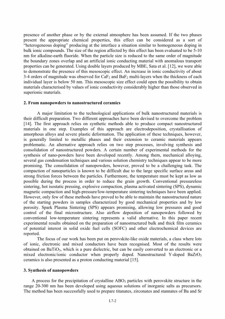
(1) Reaction (1) occurs in two steps: (i) an initial rapid formation of a gelatinous precipitate of hydrated amorphous titania; (ii) a reaction between the amorphous phase and the Ba2+ ions in the solution with formation of crystalline BaTiO3 particles. The size of the final particles is largely determined by the concentration of the reacting species and by the heating rate to the crystallisation temperature: Fig. 1 shows the effect of Ba2+ starting concentration on the kinetics of the second stage of reaction (1).
0
20
40
60
80
100
0 50 100 150 200 250 300
time (min)
Con
vers
ion
(mol
.%)..
0.062 mol/l0.0780.0950.127
Fig. 1. Formation kinetics of crystalline BaTiO3 from aqueous solutions of BaCl2 and TiCl4 at 82°C as a function of barium concentration
From the conversion curves some information about the reaction mechanism can be
obtained, mainly the existence of secondary nucleation, i.e. nucleation in the presence of solid surfaces that also explains the polycrystalline morphology of the powders prepared by this method.
Immiscible fluid
Tubular reactor
Reactants mixture
Segmenter Micromixer
Immiscible fluid
Reactant 1
Reactant 2
Fig. 2. Sketch of the Segmented Flow Tubular Reactor showing the formation of segmented micro-batch volumes
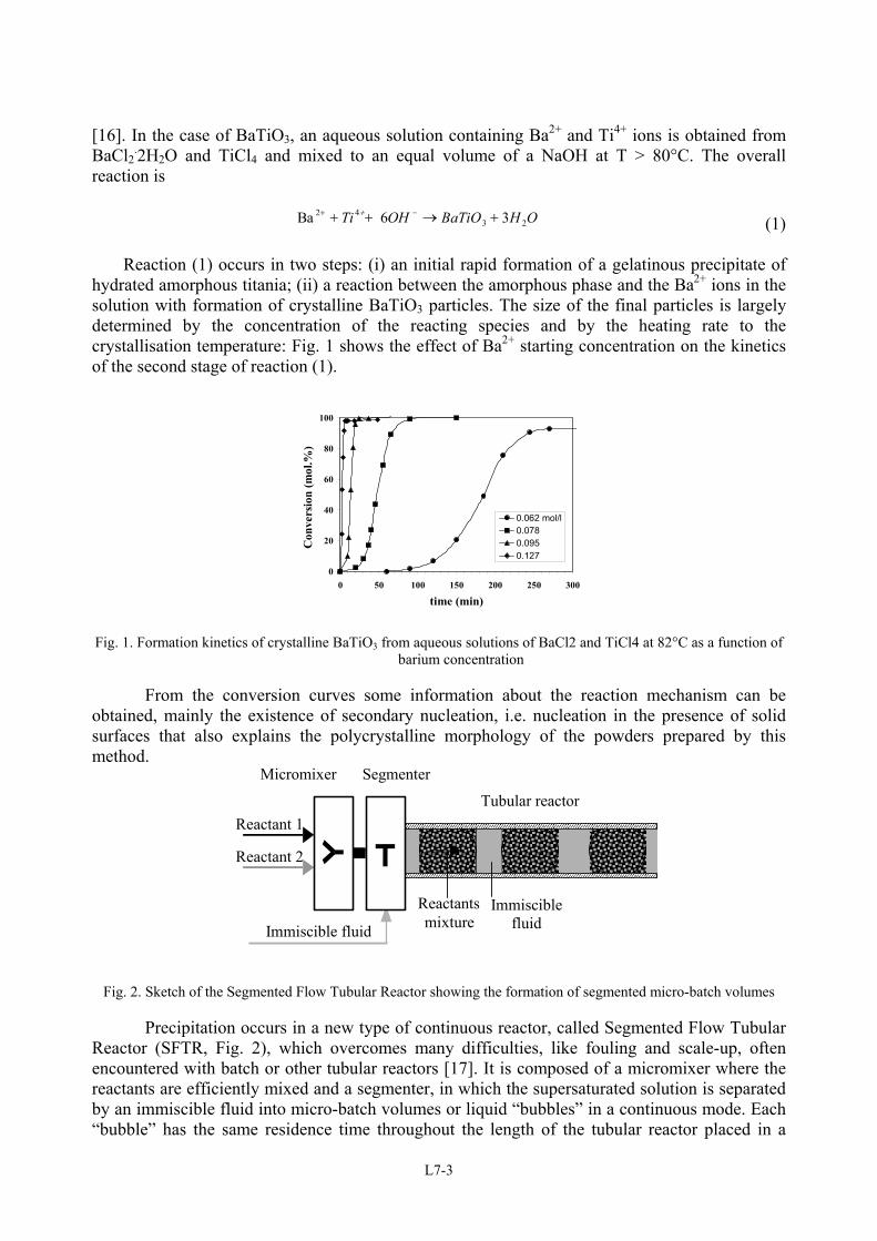
Precipitation occurs in a new type of continuous reactor, called Segmented Flow Tubular Reactor (SFTR, Fig. 2), which overcomes many difficulties, like fouling and scale-up, often encountered with batch or other tubular reactors [17]. It is composed of a micromixer where the reactants are efficiently mixed and a segmenter, in which the supersaturated solution is separated by an immiscible fluid into micro-batch volumes or liquid “bubbles” in a continuous mode. Each “bubble” has the same residence time throughout the length of the tubular reactor placed in a
L7-3
thermostatic bath. Therefore the reaction conditions that lead to the nanoparticles formation are identical for each “bubble” that acts like a real microreactor, owing to their small dimension. At the end of the tube the “bubbles” are separated from the fluid by decantation and the powder is eventually collected, washed and dried. The particles show highly homogeneous final characteristics: morphology, particle size, as well as chemical and phase composition.
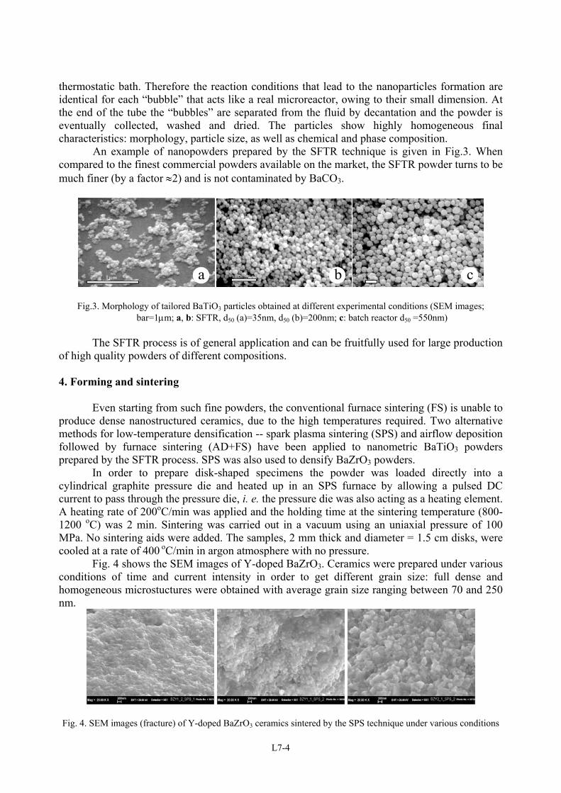
An example of nanopowders prepared by the SFTR technique is given in Fig.3. When compared to the finest commercial powders available on the market, the SFTR powder turns to be much finer (by a factor ≈2) and is not contaminated by BaCO3.
a b c
Fig.3. Morphology of tailored BaTiO3 particles obtained at different experimental conditions (SEM images;
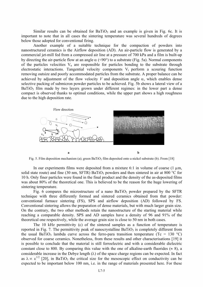
bar=1µm; a, b: SFTR, d50 (a)=35nm, d50 (b)=200nm; c: batch reactor d50 =550nm) The SFTR process is of general application and can be fruitfully used for large production of high quality powders of different compositions. 4. Forming and sintering Even starting from such fine powders, the conventional furnace sintering (FS) is unable to produce dense nanostructured ceramics, due to the high temperatures required. Two alternative methods for low-temperature densification -- spark plasma sintering (SPS) and airflow deposition followed by furnace sintering (AD+FS) have been applied to nanometric BaTiO3 powders prepared by the SFTR process. SPS was also used to densify BaZrO3 powders. In order to prepare disk-shaped specimens the powder was loaded directly into a cylindrical graphite pressure die and heated up in an SPS furnace by allowing a pulsed DC current to pass through the pressure die, i. e. the pressure die was also acting as a heating element. A heating rate of 200oC/min was applied and the holding time at the sintering temperature (800-1200 oC) was 2 min. Sintering was carried out in a vacuum using an uniaxial pressure of 100 MPa. No sintering aids were added. The samples, 2 mm thick and diameter = 1.5 cm disks, were cooled at a rate of 400 oC/min in argon atmosphere with no pressure. Fig. 4 shows the SEM images of Y-doped BaZrO3. Ceramics were prepared under various conditions of time and current intensity in order to get different grain size: full dense and homogeneous microstuctures were obtained with average grain size ranging between 70 and 250 nm.
Fig. 4. SEM images (fracture) of Y-doped BaZrO3 ceramics sintered by the SPS technique under various conditions
L7-4
Similar results can be obtained for BaTiO3 and an example is given in Fig. 6c. It is important to note that in all cases the sintering temperature was several hundreds of degrees below those adopted for conventional firing. Another example of a suitable technique for the compaction of powders into nanostructured ceramics is the Airflow deposition (AD). An air-particle flow is generated by a commercial jet-mill fed from a compressed air line at a pressure of 700 kPa and a film is built-up by directing the air-particle flow at an angle α (<90°) to a substrate (Fig. 5a). Normal components of the particles velocities Vn are responsible for particles bonding to the substrate through electrostatic interactions. Tangential velocity components Vt perform a scouring function removing outsize and poorly accommodated particles from the substrate. A proper balance can be achieved by adjustment of the flow velocity V and deposition angle α, which enables dense selective packing of submicron powder particles to be achieved. Fig. 5b shows a lateral view of a BaTiO3 film made by two layers grown under different regimes: in the lower part a dense compact is observed thanks to optimal conditions, while the upper part shows a high roughness due to the high deposition rate.
Substrate
Air + particle flow direction
Vt
V
Flow direction
α v
vt
Vnvn
a b
Fig. 5. Film deposition mechanism (a); green BaTiO3 film deposited onto a nickel substrate (b). From [18]
In our experiments films were deposited from a mixture 6:1 in volume of coarse (1 µm, solid state route) and fine (30 nm, SFTR) BaTiO3 powders and then sintered in air at 800 °C for 10 h. Only finer particles were found in the final product and the density of the as-deposited films was about 80% of the theoretical one. This is believed to be the reason for the huge lowering of sintering temperature. Fig. 6 compares the microstructure of a nano BaTiO3 powder prepared by the SFTR technique with three differently formed and sintered ceramics obtained from that powder: conventional furnace sintering (FS), SPS and airflow deposition (AD) followed by FS. Conventional sintering allows the preparation of dense materials, but with much larger grain size. On the contrary, the two other methods retain the nanostructure of the starting material while reaching a comparable density. SPS and AD samples have a density of 96 and 91% of the theoretical one respectively, while the average grain size is close to 50 nm in both cases. The 10 kHz permittivity (ε) of the sintered samples as a function of temperature is reported in Fig. 7. The permittivity peak of nanocrystalline BaTiO3 is completely different from the usual BaTiO3 lambda curve across the ferro-para transition temperature (Tc = 130 °C) observed for coarse ceramics. Nonetheless, from these results and other characterisations [19] it is possible to conclude that the material is still ferroelectric and with a considerable dielectric constant close to 800. By comparing this value with the one of alkaline-earth fluorides (≈ 8), a considerable increase in the Debye length (λ) of the space charge regions can be expected. In fact as λ ∝ ε1/2 [20], in BaTiO3 the critical size for the mesoscopic effect on conductivity can be expected to be important below 100 nm, i.e. in the range of materials presented here. For these
L7-5

reasons we believe that nanostructured perovsikte materials can be of great interest as ionically conducting materials.
(a) (b)
(c) (d)
Fig. 6. Electron microscope (SEM) images of as prepared SFTR BaTiO3 powder (a), thermally etched FS ceramic (b), chemically etched SPS ceramic (c) and surface of AD film (d)
500
600
700
800
900
40 60 80 100 120 140 160 180
Temperature (°C)
ε r'
1000
3000
5000ε r'
SPS AD FS
Fig. 7. Dielectric constant εr' vs. temperature measured at 10 kHz. Dots = FS ceramic, thin line = SPS ceramic, thick
line = AD film
5. Conclusions The preparation of dense and nanocrystalline bulk ceramics is possible when adopting well suited sintering techniques. The Spark Plasma Sintering and the Airflow Deposition have demonstrated that they can be reliable methods to obtain nanostructured perovskite materials like
L7-6

BaTiO3 and BaZrO3. Due to the persistence of ferroelectric properties for grain size below 100 nm, great enhancement of the ionic conductivity can be expected in BaTiO3 due to the mesoscopic effect. 6. Acknowledgements One of the authors (M. Viviani) would like to thank the EC for the grant that supported his participation in the Workshop (specific programme "Energy, Environment and Sustainable Development - Part B: Energy program", contract No NNE5/2002/18) 7. References 1. P. Moriarty, Rep. Prog. Phys 64 (2001) 297. 2. J. Schoonman, Solid State Ionics 135 (2000) 5. 3. Y-M. Chiang, J. Electroceramics 1-3 (1997) 205. 4. H. Gleiter, Acta Mater., 48 (2000) 1. 5. M. Cain, R. Morrell, Appl. Organomet. Chem. 15 (2001) 321. 6. N. Setter, J. Eur. Ceram. Soc. 21 (2001) 1279. 7. Y. M Chiang,E.B. Lavick, I. Kosacki, H.L. Tuller, J.Y. Ying, Appl.Phys.Lett. 69 (1996)185. 8. I. Kosacki, V.Petrovsky, H.U. Anderson, Appl.Phys.Lett. 74 (1999) 341. 9. I. Kosacki, H.U. Anderson, Solid State Ionics 97 (1997) 429. 10. J. Maier, Prog. Solid State Chem 23 (1995) 171. 11. J. Maier, J. Eur. Ceram. Soc. 19 (1999) 675. 12. N. Sata, K. Eberman, K. Eberl, J. Maier, Nature 408 (2000) 946. 13. J.S Lee, St. Adams, J. Maier, Solid State Ionics 136-137 (2000) 1261. 14. L. L Shaw, JOM 52 (2000) 41. 15. K.D. Kreuer, St. Adams, W. Munch, A. Fuchs, U. Klock, J. Maier, Solid State Ionics 145
(2001) 295. 16. M. Leoni, M. Viviani, P. Nanni and V. Buscaglia, J. Mater. Sci. Lett. 15 (1996) 1302. 17. P. Bowen P., M. Donnet, A. Testino, M. Viviani, M.T. Buscaglia, V. Buscaglia, P. Nanni,
Key Eng. Mater., 206-213 (2002) 21. 18. E. Stytsenko, M.J., Ryan, M. Daglish, J. Eur. Ceram. Soc. 24 (2004) 999. 19. Z. Zhao, V. Buscaglia, M. Viviani, M.T. Buscaglia, L. Mitoseriu, A. Testino, M. Nygren, M.
Johnsson, P. Nanni, Phys. Rev. B 70 (2004) 024107. 20. P. Knauth, H.L. Tuller, J. Am. Ceram. Soc. 85 (2002) 1654.
L7-7
Related Documents