Page 3 of 16 Nanoscale

Welcome message from author
This document is posted to help you gain knowledge. Please leave a comment to let me know what you think about it! Share it to your friends and learn new things together.
Transcript
Page 3 of 16 Nanoscale
Nanoscale
Cite this: DOI: 10.1039/c0xx00000x
www.rsc.org/xxxxxx
Dynamic Article Links
ARTICLE TYPE
This journal is © The Royal Society of Chemistry [year] [journal], [year], [vol], 00–00 | 1
Nanostructure Studies of Strongly Correlated Materials
Jiang Weia and Douglas Natelson
b
Received (in XXX, XXX) Xth XXXXXXXXX 20XX, Accepted Xth XXXXXXXXX 20XX
DOI: 10.1039/b000000x
Strongly correlated materials exhibit an amazing variety of phenomena, including metal-insulator 5
transitions, colossal magnetoresistance, and high temperature superconductivity, as strong electron-
electron and electron-phonon couplings lead to competing correlated ground states. Recently, researchers
have begun to apply nanostructure-based techniques to this class of materials, examining electronic
transport properties on previously inaccessible length scales, and applying perturbations to drive systems
out of equilibrium. We review progress in this area, particularly emphasizing work in transition metal 10
oxides (Fe3O4, VO2), manganites, and high temperature cuprate superconductors. We conclude that such
nanostructure-based studies have strong potential to reveal new information about the rich physics at
work in these materials.
Introduction
Strongly correlated materials (SCMs), in which single-particle 15
band structure is inadequate to describe the electronic and
magnetic structure, remain at the forefront of condensed matter
and materials physics research. Strong electronic correlations and
the interplay between electronic, magnetic, and structural degrees
of freedom lead to an incredibly rich panoply of phenomena.1 20
Metal-insulator transitions, “heavy” charge carriers, colossal
magnetoresistance, and the emergence of high temperature
superconductivity all have their origins in this class of materials.
From the perspective of basic science, these materials are
fascinating precisely because of the richness of emergent 25
phenomena from the collective response of the system. Their low
energy excitations can be exotic, such as having effective masses
much larger than the free electron mass, or having
unconventional properties far from those of electron-like
quasiparticles. Somehow the interactions between electrons (and 30
between electrons and the lattice) give rise to properties vastly
different from those expected from noninteracting band structure.
We are able to understand the electronic structure of a single
copper, iron, phosphorus, or oxygen atom, for example, quite
well using atomic orbitals constructed from the single-electron 35
solution to the Schroedinger equation for the Coulomb potential,
with interaction-based corrections playing a comparatively minor
role (via Hund’s rules, for example). However, magnetite (Fe3O4)
exhibits an electronic structure with a correlated ground state that
has been a topic of controversy for seven decades2, 3 and the 40
copper oxide and iron pnictide superconductors show competition
between magnetic order and superconductivity. Strongly
correlated materials are a laboratory for studying the collective
properties of large numbers of strongly interacting, highly
quantum mechanical particles. 45
These materials are also of considerable technological interest.
Room temperature superconductivity, if it occurred with the right
combination of critical current and field, would be a
transformative technology. Materials with metal-insulator
transitions and large magnetoresistive effects are attractive for 50
possible electronic switching and data storage applications.
A great deal of progress in understanding SCMs has been
made using bulk characterization techniques. These include: x-
ray, electron, and neutron diffraction to determine crystal
structures and long-range order; optical spectroscopies and 55
photoemission to learn about the electronic energetics;
magnetometry and specific heat determination to learn about
magnetic order and phase transitions; and electronic and thermal
transport, often as a function of magnetic field, to find out about
charge carrier dynamics and the mechanisms of energy flow. 60
Likewise, the development of scanned probe microscopies has
given further insights into these systems, providing evidence of
inhomogeneities on the nanoscale4, 5, and other information about
electronic structure6, 7.
Recently, however, there has been a growing realization that 65
making nanodevices based directly on SCMs enables experiments
that give information that is otherwise not readily accessible. This
article is meant to provide an overview of some of the recent
developments in this area. By its nature it is not possible in this
format to provide an exhaustive review of all work in the field. 70
We have done our best to highlight a representative set of results,
and the omission of a reference should be interpreted as an
oversight rather than a critical judgment. We consider systems
confined at the nanoscale in at least one dimension, and when
discussing two-dimensional systems we pay particular attention 75
to those with strong two-dimensional confinement. We will
describe the specific motivations for nanostructure-based SCM
investigations, briefly summarize the various ways of producing
nanostructures that incorporate SCMs, and explain why such
research has been relatively slow, compared with the application 80
of similar techniques to semiconductors and ordinary metals. We
Page 4 of 16Nanoscale
2 | Journal Name, [year], [vol], 00–00 This journal is © The Royal Society of Chemistry [year]
will then describe recent efforts, broken down by particular
families of materials. We will conclude with some observations
about the state of this approach and its likely future directions.
Nanostructure-based investigations of these materials are
motivated by specific goals directed at better understanding the 5
origins of the rich physics described above:
• Nanostructure experiments can probe SCMs on length
scales of interest. As will be demonstrated below, SCMs can
exhibit inhomogeneities in their properties, particularly
evident in phenomena such as metal-insulator or normal-10
superconductor transitions. These inhomogeneities may
involve percolation or the breakup of the SCM into domains.
Macroscale measurements average over these
inhomogeneities and can therefore obscure single-domain or
single-boundary effects. While scanned probe measurements 15
are extremely useful, there are circumstances where being
able to perform transport through an individual region,
domain, or interface is revelatory.
• Nanostructures allow discrimination between possible
physical mechanisms for phenomena. Fig. 1 shows an 20
example of a dramatic effect in a SCM. In a charge-ordered
complex oxide (praesodymium calcium manganese oxide),
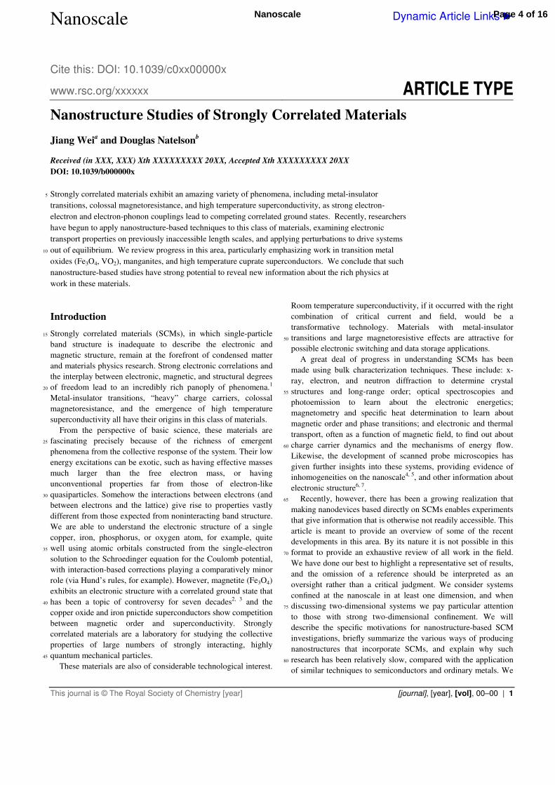
Asamitsu and collaborators observe1 that the application of
hundreds of volts across a mm-scale crystal results in a
transition from the charge-ordered insulating state to a more 25
conducting state. This change is reversible, though hysteretic,
as the voltage is reduced. It is tempting to conclude that this
represents the electric field-induced breakdown of the
correlated state. However, large energies are available to the
charge carriers in this situation, and other explanations are 30
possible. In nanoscale structures, it is possible to achieve
similar magnitudes of applied electric field while using much
lower voltages, thus placing an upper limit on the energy
available per charge carrier.
35
Fig. 1 Application of a large voltage across a ~ 1 mm crystal of a
correlated oxide in a charge-ordered insulating state results in a transition
to a more conducting state. Removal of the voltage leads to
reestablishment of the insulating state. Such large electric fields are
achievable at much lower voltages in nanostructure-based devices. 40
Reprinted by permission from MacMillan Publishers, Ltd.: Asamitsu et
al., Nature 388, 50-52 (1997), copyright 1997
• Nanostructured devices can enable gating/field-effect
experiments. In many SCM the density of charge carriers is a
tuning parameter of critical importance. Very often the carrier 45
density is altered by chemical doping, which carries with it
the necessary evil of simultaneously altering the disorder in
the material. Gating and the field-effect are a means of
altering the carrier density in a nanoscale-thickness channel at
fixed disorder.2 50
• Nanostructured devices are ideal for examining contact
effects and the process of charge injection. Conventionally,
electronic transport measurements employ multiterminal
methods to examine the intrinsic properties of the material
itself, avoiding the effects of contact resistances. In nanoscale 55
devices, contacts necessarily play an amplified role relative to
the bulk. This can be an opportunity rather than a problem. In
many SCMs, the low energy excitations are collective objects
with quantum numbers that differ greatly from those of the
electron-like quasiparticles in ordinary metals. When an 60
electron is injected into such a SCM, there is a ”dressing”
process that must take place, and contact/charge injection
experiments are the natural way to probe this.
• Nanostructured devices are essential for probing the
nonequilibrium physics of SCMs. The nonequilibrium 65
response of SCMs can be dramatic and provides another
probe of the electronic states and their excitations in such
materials. Applying a voltage bias to a SCM drives the local
electronic (and vibrational) distributions out of equilibrium.
Deviations from equilibrium distributions persist on length 70
scales associated with inelastic processes. Any effort to
measure these deviations, through tunneling3, 4, or shot noise5,
must be made using devices that are comparable in scale to
the inelastic scattering length. In SCMs, this distance can
easily be on the nanoscale, requiring electrodes spaced 75
accordingly.
Nanoscale devices may be made from SCMs by a variety of
techniques, many of which are based on approaches developed in
the study and engineering of semiconductors. The simplest is
direct growth of the material into a form useful for nanoscale 80
study. For two-dimensional structures or superlattices, molecular
beam epitaxy and pulsed laser deposition have been invaluable.6, 7
Some SCMs may be grown in even further reduced
dimensionality, as in VO2 nanowires8 produced from the vapor
phase, or nanowires made via templating9, 10. Exfoliation of 85
layered materials is also possible.11
More traditionally, lithographic techniques may be combined
with thin film growth to achieve SCM-based nanostructures.
Electrodes may be fabricated with nanoscale separations directly
on the surfaces of bulk or thin-film SCMs.12, 13 Films of strongly 90
correlated materials may be subtractively patterned into
nanostructures via lithographic definement of features and
chemical etching14-16. Additive patterning via lift-off processing
is also possible under some circumstances17, 18, though that
requires the growth of the SCM in the presence of some material 95
that may be used as a resist.
The patterning required for device fabrication is one reason
why nanostructured studies of SCM are often challenging.
Stoichiometry is often critical to the character of the ground states
exhibited in SCMs, as exemplified in the cuprate 100
Page 5 of 16 Nanoscale
This journal is © The Royal Society of Chemistry [year] Journal Name, [year], [vol], 00–00 | 3
superconductors. The parent compound of the typical cuprate is a
Mott insulator, and depending on the chemical doping (including
alteration of the oxygen content) the ground state of the material
may be an antiferromagnet, a “strange” (non-Fermi liquid) metal,
an unconventional superconductor, or a comparatively normal 5
metal. Preserving stoichiometry in nanostructured materials can
be difficult. In nanostructured form, materials have large surface
to volume ratios, and oxidation or surface reconstruction must be
a concern. Similarly, in nanostructures produced by top-down
patterning of films or bulk materials, exposure of the material to 10
processing conditions (chemical etchants, lithography,
“descumming” techniques) can chemically modify the material
away from the desired composition.
Transition Metal Oxides
Strong correlations are frequently associated with materials 15
containing partially filled orbitals of a comparatively localized
character. Transition metal oxides, with their partially filled d
shells, fit the bill, and can exhibit dramatic deviations from
single-electron band structure expectations. NiO, for example, is
a transparent insulator when conventional band structure would 20
predict metallic conduction19. Here we discuss recent
nanostructure-based experiments on two particular transition
metal oxide systems.
Magnetite
Magnetite, Fe3O4, also known as lodestone, has been known for 25
thousands of years due to its magnetic properties. The oxide
contains two populations of iron atoms, the A-sites (formal
valence +3, tetrahedrally coordinated by oxygens) and the B-sites
(formally mixed valence, split between +2 and +3, octahedrally
coordinated by oxygens). The iron sites order ferrimagnetically at 30
a temperature of 848 K. At room temperature, Fe3O4 is an inverse
spinel with a large, cubic unit cell, and is moderately conductive,
with a resistivity of a few mΩ-cm. Conduction is takes place
through the hopping of charge among the d orbitals of the mixed-
valence B-site irons. As temperature is reduced, the resistivity 35
increases weakly. At a temperature of around 122 K in the bulk,
magnetite undergoes what is now known as the Verwey
transition20, a first-order phase transition to a more resistive state,
with a monoclinic unit cell. A similar transition is also observed
in other inverse spinels, and magnetite is therefore an archetype 40
of this kind of “metal”-insulator transition21. Verwey’s original
hypothesis for this transition, that of simple charge ordering of
the B-site iron valence, has been ruled out via diffraction
experiments22. However, controversy remains concerning the
nature of the Verwey ground state and the relative importance of 45
electronic correlations and the electron-phonon coupling.
One challenge in investigating the Verwey transition through
nanostructures is the sensitivity of the transition to oxygen
content23, 24. A deviation from ideal oxygen stoichiometry by only
a couple of percent completely suppresses the transition 50
temperature, TV, leading instead to a smoothly increasing
resistivity upon cooling. This sensitivity, combined with the
relative stability of other iron oxides, hematite (Fe2O3) and
wustite (FeO), implies that nanoscale magnetite studies may be
hampered by either oxidation or reduction of the material at its 55
surface. Some experiments with magnetite nanoparticles25 report
suppression of the Verwey transition with decreasing particle
size, while others show persistence of the transition even in sub-
10 nm nanoparticles26.
60
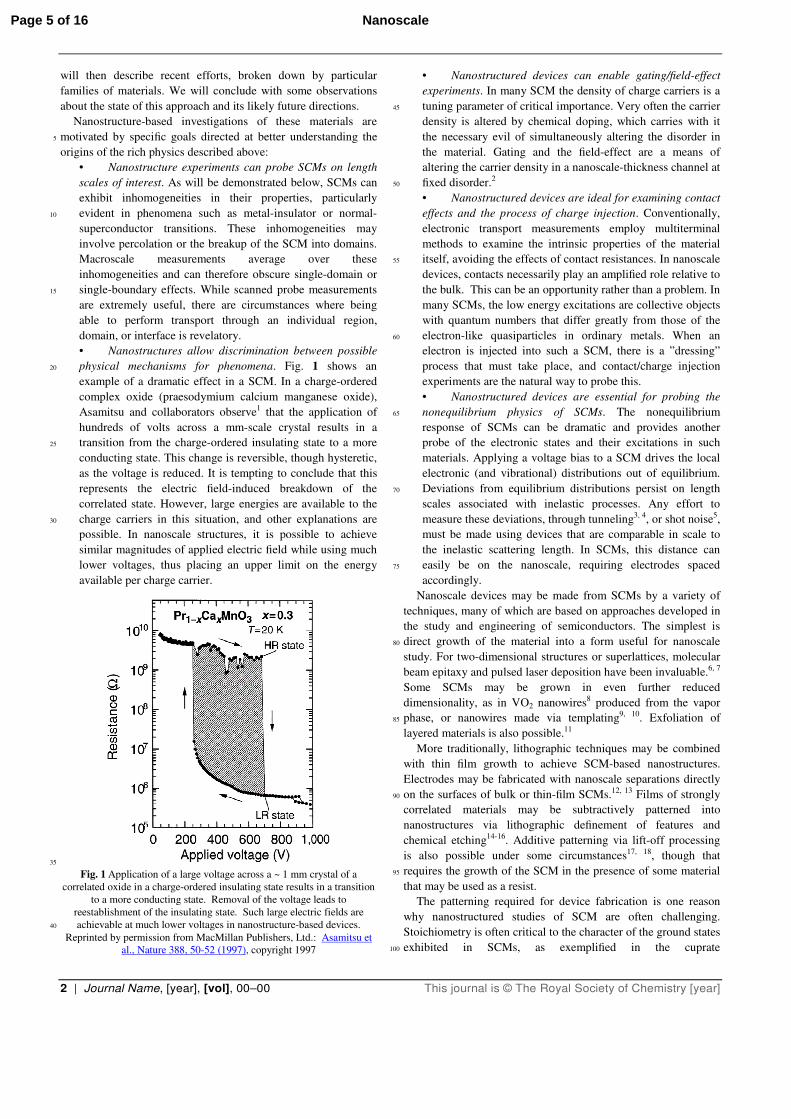
Fig. 2 (a) In magnetite nanostructures, the low-temperature, insulating Verwey state is destabilized at large applied voltages, similar to what is seen in Fig.
1. Adapted with permission from MacMillan Publishers, Ltd.: from Lee et al., Nature Mater. 7, 130-133 (2008).
(b) The switching voltage varies linearly with the length of the magnetite channel, consistent with an electric field-driven transition. A. A. Fursina et al.,
unpublished.
Recent studies using nanospaced electrodes with both Fe3O4 65
nanoparticles27 and epitaxially grown, single-crystal thin films12,
27 have revealed the existence of a nonequilibrium transition in
Fe3O4 at temperatures below TV. In the low temperature state, a
sufficiently large dc voltage in a given device drives the material
out of the insulating state and back into a more conducting state, 70
as shown in Fig. 2a. This transition, in which the material returns
to the insulating state as the bias voltage is reduced, is
reminiscent of that shown in Fig. 1, hypothesized to be the result
of field-driven breakdown of a charge-ordered ground state.
Page 6 of 16Nanoscale
4 | Journal Name, [year], [vol], 00–00 This journal is © The Royal Society of Chemistry [year]
Defining the switching voltage, Vsw(T), as the voltage at which
the device switches to the high-conductance state as the
magnitude of the applied voltage is increased, Fig. 2a shows that
Vsw increases as T is decreased below Vsw, and that the transition
vanishes as T → TV, where TV is determined by the temperature 5
dependence of the zero bias resistance.
In standard non-volatile resistive switching28, 29, sweeping an
applied voltage results in a change in the resistance of a device
that persists when the bias is reduced back to zero (“non-
volatile”). A second voltage sweep is required to recover the 10
original resistance. Note that the transition observed in magnetite
is not nonvolatile, and is not “resistive switching” as described by
the nonvolatile memory community.
In the magnetite case, it is possible to test for the field-driven
character of the transition by examining the geometric scaling of 15
the device characteristics. As shown in Fig. 2b, Vsw varies
approximately linearly with L, the interelectrode separation,
indicating that at any given temperature there is a characteristic
electric field, dVsw/dL, associated with the nonequilibrium
transition. For TV ≈ 110 K, the critical field scale is approximately 20
4 × 10⁶ V/m at 100 K and 8 × 10⁶ V/m at 80 K. Note that the
amount of energy gained by an electron tunneling across one unit
cell in such a field at 80 K would be about 7 meV, comparable to
kBTV. This is consistent with the scenario that the nonequilibrium
transition is a Landau-Zener-like breakdown of the correlated 25
state30, 31.
The hysteresis apparent in Fig. 2a is now known to be a result
of self-heating32. Once the device is switched into the conducting
state, power dissipation due to increased current flow elevates the
local temperature so that Vsw is reduced, leading to hysteresis if 30
the bias voltage is continuously swept. Measurements with 0.5
ms pulses have shown that the hysteresis vanishes, while Vsw(T)
remains essentially unaltered, in the limit of short, well-separated
pulses. High speed pulsed measurements33 indicate that
switching takes place on timescales of tens of nanoseconds. 35
X
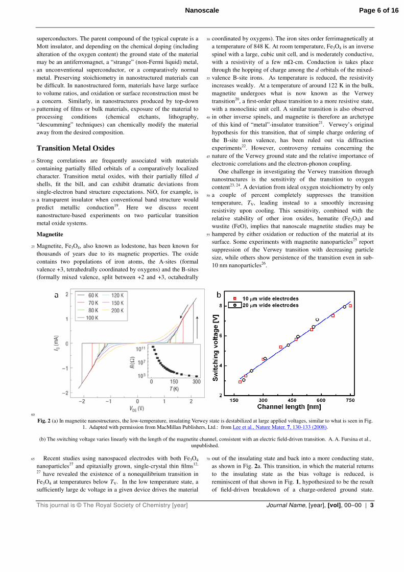
Fig. 3 (a) Multiterminal measurements allow the determination of both bulk and contact resistances in magnetite nanostructures. As is clear from inset
(d), the bulk and contact resistances have identical temperature dependences. Reprinted with permission from A. A. Fursina et al., Phys. Rev. B 81,
045123 (2010). Copyright 2010 by the American Physical Society. (b) This trend is true for several different contact metals, and by analogy with similar
observations in organic semiconductor devices, implies that conduction in both the high and low temperature states takes place through a hopping 40
mechanism. This is an example of using contact measurements to infer bulk transport physics. Reprinted with permission from A. A. Fursina et al., Phys.
Rev. B 82, 245112 (2010). Copyright 2010 by the American Physical Society.
Vsw does not extrapolate to zero as L → 0 because some
fraction of the applied voltage is dropped at the injecting and 45
collecting contacts. Using multiterminal measurements, as shown
in Fig. 3a, it has been possible to study the contact resistance in
such structures as well as the bulk resistivity34, 35. Two important
observations came from these measurements. First, at Vsw, the
contact resistances at both the injecting and collecting electrodes 50
drop, as well as the bulk resistance; this is again consistent with a
field-driven breakdown of the correlated state30, 31 Second, the
contact resistance was found to have the same temperature
dependence as the bulk resistance, from room temperature down
to well below TV. This trend is true for multiple contact metals 55
(Cu, Au, Pt), as shown in Fig. 3b.
The apparent proportionality between the bulk resistivity and
the contact resistance over the whole temperature range
demonstrates the power of contact studies to access the bulk
transport mechanism in a SCM. Such a proportionality has been 60
observed previously36, 37 in organic semiconductor structures in
which transport in the bulk is dominated by carrier hopping
between localized states. For charge injection from a metal into a
hopping system, an injected carrier can diffuse away from the
interface via hopping, but at the same time is influenced by its 65
image charge in the metal. This competition leads38 to a contact
resistance that is inversely proportional to the charge mobility,
and hence directly proportional to the resistivity, of the hopping
system. The magnetite contact measurements therefore confirm
that conduction in both the low and high temperature states of 70
magnetite proceeds through hopping39, consistent with observed
temperature dependences, and may permit further studies of the
nature of the mobile charge carriers.
Vanadium Dioxide
VO2 is famous for its dramatic metal-insulator transition with up 75
Page 7 of 16 Nanoscale
This journal is © The Royal Society of Chemistry [year] Journal Name, [year], [vol], 00–00 | 5
to four orders magnitude40 change in conductivity at 67oC - a
convenient temperature for many applications. Below 67oC, VO2
is semiconductor (the M1 phase) featuring a gap about 0.7 eV41, 42
with a monoclinic crystal structure, while above 67oC the lattice
transforms into a bad metal with a rutile structure. The long-term 5
debated mechanism43, 44 of the metal-insulator transition is still
obscure. The lattice structure change suggests a first-order phase
transition where the vanadium chain dimerizes during the
transition, causing the size of the unit cell to double. This
supports a Peierls-like transition from the view of band theory. 10
However, many factors point to a Mott transition, driven by
strong electron-electron interactions. These factors include the
anomalously low conductivity of the metallic state;45-47 the fact
that band structure calculations fail to obtain the insulator band
gap;44, 48 the fact that an intermediate monoclinic “M2” phase, 15
which can be stabilized by stress49 or doping,50 is insulating in
spite of having undimerized vanadium chains;43 and in optical
experiments a dependence of properties on excitation power
which indicates sensitivity to excited carrier density.51-53
Despite the dramatic MIT at a convenient temperature, 20
seemingly easy applications of VO2 in electrical54 and optical55
switching or sensors remain unrealized. The blame for this falls
largely on the large strains associated with the structural
transition. The resulting stresses lead to cracking in bulk VO2
crystals, and the formation of a complicated metal/insulator 25
domain structure (consequently affecting measured resistance) in
films and large particles upon passing through the MIT. The
result is often irreproducibility between samples, broadening and
hysteresis of the characteristics, and mechanical degradation.
X 30
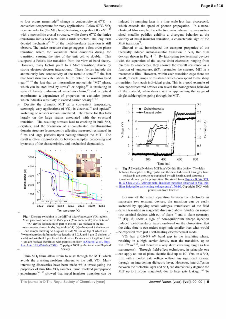
Fig. 4 Discrete switching in the MIT of micro/nanoscale VO2 regions.
Main panel—8 consecutive R-T cycles (R in linear scale) of a 1x 6µm2
VO2 device zoomed in on part of the MIT, as marked in the full
measurement shown in (b) (log scale of R). (a)—Image of 8 devices on
one sample showing VO2 square of side 50 µm, on top of which are 35
V=Au electrodes defining device lengths of 1,2,3, and 4 µm (2 devices of
each) and width of 8 µm for all the devices. Devices with length of 1 and
4 µm are marked. Reprinted with permission from A.Sharoni et al., Phys.
Rev. Lett. 101, 026404 (2008). Copyright 2008 by the American Physical
Society. 40
Thin VO2 films allow strain to relax through the MIT, which
avoids the cracking problem inherent to the bulk VO2. Many
interesting discoveries have been made while investigating the
properties of thin film VO2 samples. Time resolved pump-probe
experiments56, 57 showed that metal-insulator transition can be 45
induced by pumping laser in a time scale less than picosecond,
which exceeds the speed of phonon propagation. In a nano-
clustered film sample, the effective mass inferred in nanometer-
sized metallic puddles exhibits a divergent behavior at the
vicinity of metal-insulator transition, a characteristic sign of the 50
Mott transition58.
Sharoni et al. investigated the transport properties of the
thermally induced metal-insulator transition in VO2 thin film
devices shown in Fig. 4 13. By fabricating two terminal devices
with the separation of the source drain electrodes ranging from 55
microns to nanometers, they showed the overall resistance as a
function of temperature, R(T), resembles the smeared MIT in a
macroscale film. However, within each transition edge there are
small, discrete jumps of resistance which correspond to the sharp
transition from each individual grain. This is a good example of 60
how nanostructured devices can reveal the homogenous behavior
of the material, when device size is approaching the range of
single stable regions going through the MIT.
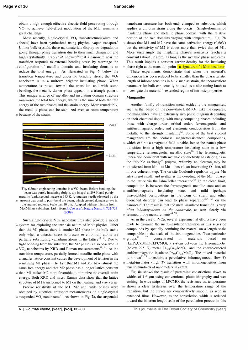
Fig. 5 Electrically driven MIT in a VO2 thin film device. The delay 65
between the applied voltage pulse and the detected current through a load
resistor is too short to be explained by self-heating, and supports a
transition driven by charge injection. Reprinted from Physica B, Vol 369,
B.-G. Chae et al., “Abrupt metal-insulator transition observed in VO2 thin
films induced by a switching voltage pulse”, 76-80, Copyright 2005, with 70
permission from Elsevier.
Because of the small separation between the electrodes in
nanoscale two terminal devices, the transition can be easily
switched by applying small voltages, reminiscent of the field
driven transition in magnetite discussed above. Studies on simple 75
two-terminal devices with out of plane 59 and in plane geometry 60 (Fig. 5) show a sign of non-equilibrium charge injection
induced metal-insulator transition-based on the observation that
the delay time is two orders magnitude smaller than what would
be expected from just a self-heating electrothermal model. 80
VO2 has a 0.6-0.7 eV band gap in the insulating phase,
resulting in a high carrier density near the transition, up to
2x10¹⁸/cm-3 61, and therefore a very short screening length (a few
nanometers). Through field-effect techniques, in principle one
can apply an out-of-plane electric field up to 107 V/m on a VO2 85
film with a modest gate voltage without any significant leakage
through an intervening dielectric layer. However, interdiffusion
between the dielectric layer and VO2 can dramatically degrade the
MIT up to 2 orders magnitude due to large gate leakage. 61 To
Page 8 of 16Nanoscale
6 | Journal Name, [year], [vol], 00–00 This journal is © The Royal Society of Chemistry [year]
obtain a high enough effective electric field penetrating through
VO2 to achieve field-effect modulation of the MIT remains a
great challenge.
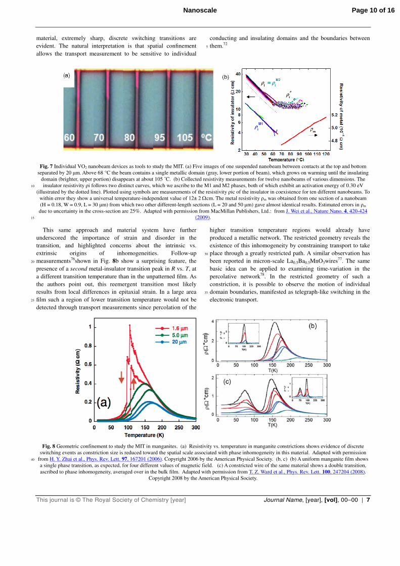
Most recently, single-crystal VO2 nanostructures(wires and
sheets) have been synthesized using physical vapor transport.8 5
Unlike bulk crystals, these nanomaterials display no degradation
going through phase transition due to their small dimension and
high crystallinity. Cao et al. showed62 that a nanowire near the
transition responds to external bending stress by rearrange the
configuration of metallic domain and insulating domains to 10
reduce the total energy. As illustrated in Fig. 6, below the
transition temperature and under no bending stress, the VO2
nanobeam is in a uniform brighter insulating phase. When
temperature is raised toward the transition and with some
bending, the metallic darker phase appears in a triangle pattern. 15
This unique arrange of metallic and insulating domain structure
minimizes the total free energy, which is the sum of both the free
energy of the two phases and the strain energy. More remarkably,
the metallic phase can be stabilized even at room temperature
because of the strain. 20
Fig. 6 Strain engineering domains in a VO2 beam. Before bending, the
beam was purely insulating (bright, top image) at 298 K and purely
metallic (dark, second image) at 343 K. A tungsten needle (denoted by the
arrows) was used to push-bend the beam, which created domain arrays in 25
the strained regions. Scale bar, 10 µm. Adapted with permission from
MacMillan Publishers, Ltd.: from J. Cao et al., Nature Nano. 4, 732-737
(2009).
Such single crystal VO2 nanostructures also provide a model
system for exploring the intrinsic nature of Mott physics. Other 30
than the M1 phase, there is another M2 phase in the bulk stable
only when a uniaxial stress is present or chromium atoms are
partially substituting vanadium atoms in the lattice49, 50. Due to
tight bonding from the substrate, the M2 phase is also observed in
VO2 nanobeams by XRD and Raman measurements63, 64. At the 35
transition temperature, partially formed metallic rutile phase with
a smaller lattice constant causes the development of tension in the
remaining M1 phase. The fact that M1 and M2 have almost the
same free energy and that M2 phase has a longer lattice constant
than M1 makes M2 more favorable to minimize the overall strain 40
energy. Both XRD and micro-Raman data show that the lattice
structure of M1 transformed to M2 on the heating, and vise versa.
Precise resistivity of the M1, M2 and rutile phases were
obtained by electrical transport measurements on single-crystal
suspended VO2 nanobeams42. As shown in Fig. 7a, the suspended 45
nanobeam structure has both ends clamped to substrate, which
applies a uniform strain along the c-axis. Single-domains of
insulating phase and metallic phase coexist, with the relative
portion of the two domains varying with temperature. Fig. 7b
shows that M1 and M2 have the same activation energy (0.6eV) 50
but the resistivity of M2 is about more than twice that of M1.
More surprisingly the insulating phase’s resistivity reaches a
constant (about 12 Ωcm) as long as the metallic phase nucleates.
This result implies a constant carrier density for the insulating
phase right at the transition point - a signature of a Mott insulator. 55
These experiments demonstrate that when the material’s
dimension has been reduced to be smaller than the characteristic
length of inhomogeneities in bulk such as strain, the inconvenient
parameter for bulk can actually be used as a nice tuning knob to
investigate the material’s extended region of intrinsic properties. 60
Manganites
Another family of transition metal oxides is the manganites,
such as that based on the perovskite LaMnO3. Like the cuprates,
the manganites have an extremely rich phase diagram depending
on their chemical doping, with many competing phases including 65
those with charge order, orbital order, ferromagnetic, and
antiferromagnetic order, and electronic conductivities from the
metallic to the strongly insulating65. Some of the best studied
manganites are the “colossal magnetoresistance” compounds,
which exhibit a (magnetic field-tunable, hence the name) phase 70
transition from a high temperature insulating state to a low
temperature ferromagnetic metallic state66. The ferromagnetic
interaction coincident with metallic conductivity has its origins in
the “double exchange” process, whereby an electron may be
transferred from Mn3+
to Mn4+
ions via an intervening O2−
ion, all 75
in one coherent step. The on-site Coulomb repulsion on the Mn
sites is not small, and neither is the coupling of the Mn4+
charge
to the lattice via the Jahn-Teller interaction65. In the clean limit,
competition is between the ferromagnetic metallic state and an
antiferromagnetic insulating state, and mild (perhaps 80
unavoidable) perturbations in the form of strain and other
quenched disorder can lead to phase separation67, 68 on the
nanoscale. The result is that the metal-insulator transition is very
often inhomogeneous on the nanoscale, as seen clearly via
scanned probe measurements69, 70. 85
As in the case of VO2, several experimental efforts have been
made to examine the metal-insulator transition in this series of
compounds by spatially confining the materal on a length scale
comparable to the scale of the inhomogeneities. Two particular
groups71, 72 concentrated on materials based on 90
(La,Pr,Ca)MnO3(LPCMO), a system between the ferromagnetic
(below 275 K) metal La5/8Ca3/8MnO3, and the charge-ordered
antiferromagnetic insulator Pr5/8Ca3/8MnO3. The mixed material
is known73-75 to exhibit a percolative, inhomogeneous (low T)
metal-insulator (high T) transition with inhomogeneities from 95
tens to hundreds of nanometers in extent.
Fig. 8a shows the result of patterning constrictions down to
widths of 1.6 µm using conventional photolithography and wet
etching. In wide strips of LPCMO, the resistance vs. temperature
shows a clear hysteresis over the temperature range of the 100
transition, but the curves are comparatively smooth, as seen in
extended films. However, as the constriction width is reduced
toward the inherent length scale of the percolation process in this
Page 9 of 16 Nanoscale
This journal is © The Royal Society of Chemistry [year] Journal Name, [year], [vol], 00–00 | 7
material, extremely sharp, discrete switching transitions are
evident. The natural interpretation is that spatial confinement
allows the transport measurement to be sensitive to individual
conducting and insulating domains and the boundaries between
them.72 5
Fig. 7 Individual VO2 nanobeam devices as tools to study the MIT. (a) Five images of one suspended nanobeam between contacts at the top and bottom
separated by 20 µm. Above 68 °C the beam contains a single metallic domain (gray, lower portion of beam), which grows on warming until the insulating
domain (brighter, upper portion) disappears at about 105 ˚C. (b) Collected resistivity measurements for twelve nanobeams of various dimensions. The
insulator resistivity ρi follows two distinct curves, which we ascribe to the M1 and M2 phases, both of which exhibit an activation energy of 0.30 eV 10
(illustrated by the dotted line). Plotted using symbols are measurements of the resistivity ρic of the insulator in coexistence for ten different nanobeams. To
within error they show a universal temperature-independent value of 12± 2 Ωcm. The metal resistivity ρm was obtained from one section of a nanobeam
(H = 0.18, W = 0.9, L = 30 µm) from which two other different-length sections (L = 20 and 50 µm) gave almost identical results. Estimated errors in ρm
due to uncertainty in the cross-section are 25%. Adapted with permission from MacMillan Publishers, Ltd.: from J. Wei et al., Nature Nano. 4, 420-424
(2009). 15
This same approach and material system have further
underscored the importance of strain and disorder in the
transition, and highlighted concerns about the intrinsic vs.
extrinsic origins of inhomogeneities. Follow-up
measurements76shown in Fig. 8b show a surprising feature, the 20
presence of a second metal-insulator transition peak in R vs. T, at
a different transition temperature than in the unpatterned film. As
the authors point out, this reemergent transition most likely
results from local differences in epitaxial strain. In a large area
film such a region of lower transition temperature would not be 25
detected through transport measurements since percolation of the
higher transition temperature regions would already have
produced a metallic network. The restricted geometry reveals the
existence of this inhomogeneity by constraining transport to take
place through a greatly restricted path. A similar observation has 30
been reported in micron-scale La0.5Ba0.5MnO3wires77. The same
basic idea can be applied to examining time-variation in the
percolative network78. In the restricted geometry of such a
constriction, it is possible to observe the motion of individual
domain boundaries, manifested as telegraph-like switching in the 35
electronic transport.
Fig. 8 Geometric confinement to study the MIT in manganites. (a) Resistivity vs. temperature in manganite constrictions shows evidence of discrete
switching events as constriction size is reduced toward the spatial scale associated with phase inhomogeneity in this material. Adapted with permission
from H. Y. Zhai et al., Phys. Rev. Lett. 97, 167201 (2006). Copyright 2006 by the American Physical Society. (b, c) (b) A uniform manganite film shows 40
a single phase transition, as expected, for four different values of magnetic field. (c) A constricted wire of the same material shows a double transition,
ascribed to phase inhomogeneity, averaged over in the bulk film. Adapted with permission from T. Z. Ward et al., Phys. Rev. Lett. 100, 247204 (2008).
Copyright 2008 by the American Physical Society.
Page 10 of 16Nanoscale
Nanoscale
Cite this: DOI: 10.1039/c0xx00000x
www.rsc.org/xxxxxx
Dynamic Article Links
ARTICLE TYPE
This journal is © The Royal Society of Chemistry [year] [journal], [year], [vol], 00–00 | 8
Recent experiments have considered the LPCMO system at
even smaller constricted widths, well below 1 µm, fabricated via
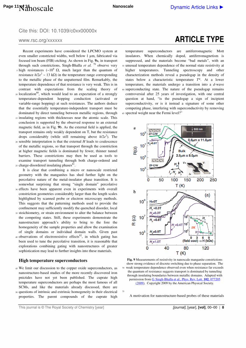
focused ion beam (FIB) etching. As shown in Fig. 9a, in transport
through such constrictions, Singh-Bhalla et al. 79 observe very
high resistances (~108
Ω, much larger than the quantum of 5
resistance h/2e2 ~ 13 kΩ) in the temperature range corresponding
to the metallic phase of the unpatterned film. Remarkably, the
temperature dependence of that resistance is very weak. This is in
contrast with expectations from the scaling theory of
localization80, which would lead to an expectation of a strongly 10
temperature-dependent hopping conduction (activated or
variable-range hopping) at such resistances. The authors deduce
that the essentially temperature-independent transport must be
dominated by direct tunneling between metallic regions, through
insulating regions with thicknesses near the atomic scale. This 15
conclusion is supported by the observed response to an external
magnetic field, as in Fig. 9b. As the external field is applied, the
transport remains only weakly dependent on T, but the resistance
drops considerably (while still remaining above h/2e2). The
sensible interpretation is that the external H leads to coalescence 20
of the metallic regions, so that transport through the constriction
at higher magnetic fields is dominated by fewer, thinner tunnel
barriers. These constrictions may then be used as tools to
examine transport tunneling through both charge-ordered and
charge-disordered insulating phases81. 25
It is clear that combining a micro or nanoscale restricted
geometry with the manganites has shed further light on the
percolative nature of the metal-insulator phase transition. It is
somewhat surprising that strong “single domain” percolative
effects have been apparent even in experiments with overall 30
constriction geometries considerably larger than the length scales
highlighted by scanned probe or electron microscopy methods.
This suggests that the patterning methods used to provide the
confinement may sufficiently modify the quenched disorder, local
stoichiometry, or strain environment to alter the balance between 35
the competing states. Still, these experiments demonstrate the
nanostructure approach’s ability to bring to the fore the
homogeneity of the sample properties and allow the examination
of single domains or individual domain walls. Given past
observations of electroresistive effects82, in which gating has 40
been used to tune the percolative transition, it is reasonable that
explorations combining gating with nanostructures of greater
sophistication may lead to further insights into these materials.
High temperature superconductors
We limit our discussion to the copper oxide superconductors, as 45
nanostructure-based studies of the more recently discovered iron
pnictides have not yet been published. The cuprate high
temperature superconductors are perhaps the most famous of all
SCMs, and like the materials already discussed, there are
questions of intrinsic and extrinsic homogeneity in their electrical 50
properties. The parent compounds of the cuprate high
temperature superconductors are antiferromagnetic Mott
insulators. When chemically doped, antiferromagnetism is
suppressed, and the materials become “bad metals”, with an
unusual temperature dependence of the normal state resistivity at 55
higher temperatures. Tunneling spectroscopy and other
characterization methods reveal a pseudogap in the density of
states below a characteristic temperature T*. At a lower
temperature, the materials undergo a transition into a d-wave
superconducting state. The nature of the pseudogap remains 60
controversial after 25 years of investigation, with one central
question at hand, “is the pseudogap a sign of incipient
superconductivity, or is it instead a signature of some other
competing phase, interfering with superconductivity by removing
spectral weight near the Fermi level?” 65
Fig. 9 Measurements of resistivity in nanoscale manganite constrictions
show strong evidence of discrete switching due to phase separation. The
weak temperature dependence observed even when resistance far exceeds 70
the quantum of resistance suggests transport is dominated by tunneling
through insulating boundaries between metallic domains. Adapted with
permission from G. Singh-Bhalla et al., Phys. Rev. Lett. 102, 077205
(2009). Copyright 2009 by the American Physical Society.
75
A motivation for nanostructure-based probes of these materials
Page 11 of 16 Nanoscale
This journal is © The Royal Society of Chemistry [year] Journal Name, [year], [vol], 00–00 | 9
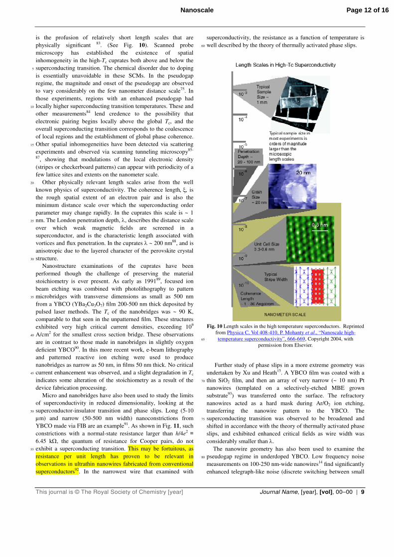
is the profusion of relatively short length scales that are
physically significant 83. (See Fig. 10). Scanned probe
microscopy has established the existence of spatial
inhomogeneity in the high-Tc cuprates both above and below the
superconducting transition. The chemical disorder due to doping 5
is essentially unavoidable in these SCMs. In the pseudogap
regime, the magnitude and onset of the pseudogap are observed
to vary considerably on the few nanometer distance scale75. In
those experiments, regions with an enhanced pseudogap had
locally higher superconducting transition temperatures. These and 10
other measurements84 lend credence to the possibility that
electronic pairing begins locally above the global Tc, and the
overall superconducting transition corresponds to the coalescence
of local regions and the establishment of global phase coherence.
Other spatial inhomogeneities have been detected via scattering 15
experiments and observed via scanning tunneling microscopy85-
87, showing that modulations of the local electronic density
(stripes or checkerboard patterns) can appear with periodicity of a
few lattice sites and extents on the nanometer scale.
Other physically relevant length scales arise from the well 20
known physics of superconductivity. The coherence length, ξ, is
the rough spatial extent of an electron pair and is also the
minimum distance scale over which the superconducting order
parameter may change rapidly. In the cuprates this scale is ~ 1
nm. The London penetration depth, λ, describes the distance scale 25
over which weak magnetic fields are screened in a
superconductor, and is the characteristic length associated with
vortices and flux penetration. In the cuprates λ ~ 200 nm88, and is
anisotropic due to the layered character of the perovskite crystal
structure. 30
Nanostructure examinations of the cuprates have been
performed though the challenge of preserving the material
stoichiometry is ever present. As early as 199189, focused ion
beam etching was combined with photolithography to pattern
microbridges with transverse dimensions as small as 500 nm 35
from a YBCO (YBa2Cu3O7) film 200-500 nm thick deposited by
pulsed laser methods. The Tc of the nanobridges was ~ 90 K,
comparable to that seen in the unpatterned film. These structures
exhibited very high critical current densities, exceeding 109
A/cm2 for the smallest cross section bridge. These observations 40
are in contrast to those made in nanobridges in slightly oxygen
deficient YBCO90. In this more recent work, e-beam lithography
and patterned reactive ion etching were used to produce
nanobridges as narrow as 50 nm, in films 50 nm thick. No critical
current enhancement was observed, and a slight degradation in Tc 45
indicates some alteration of the stoichiometry as a result of the
device fabrication processing.
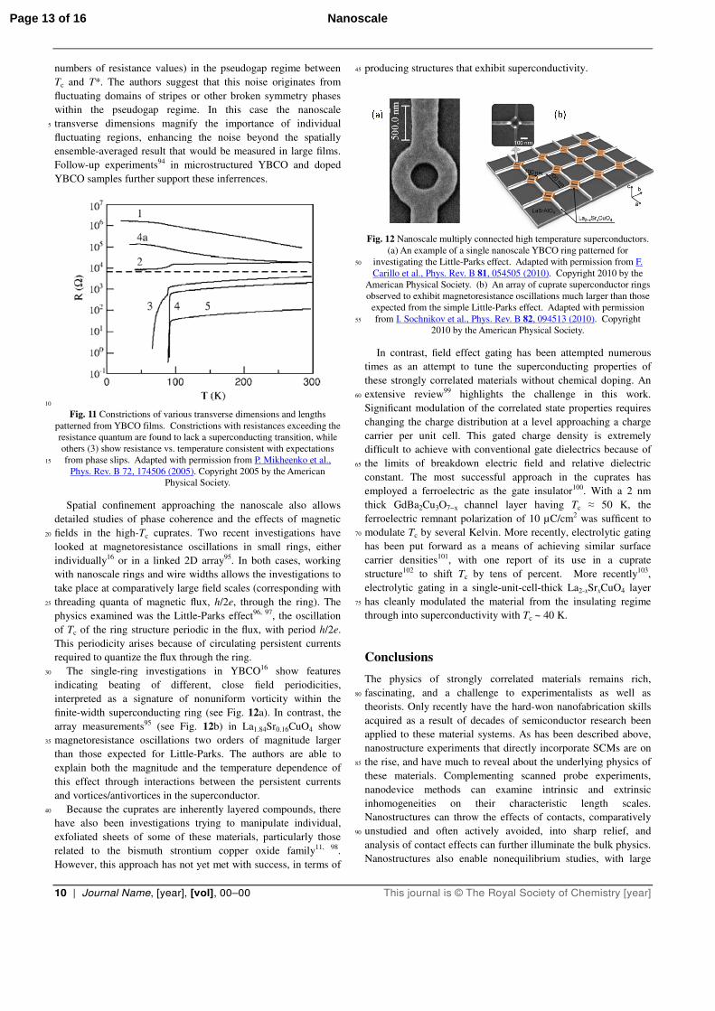
Micro and nanobridges have also been used to study the limits
of superconductivity in reduced dimensionality, looking at the
superconductor-insulator transition and phase slips. Long (5-10 50
µm) and narrow (50-500 nm width) nanoconstrictions from
YBCO made via FIB are an example91. As shown in Fig. 11, such
constrictions with a normal-state resistance larger than h/4e2 = 6.45 kΩ, the quantum of resistance for Cooper pairs, do not
exhibit a superconducting transition. This may be fortuitous, as 55
resistance per unit length has proven to be relevant in
observations in ultrathin nanowires fabricated from conventional
superconductors92. In the narrowest wire that examined with
superconductivity, the resistance as a function of temperature is
well described by the theory of thermally activated phase slips. 60
Fig. 10 Length scales in the high temperature superconductors. Reprinted
from Physica C, Vol 408-410, P. Mohanty et al., “Nanoscale high-
temperature superconductivity”, 666-669, Copyright 2004, with 65
permission from Elsevier.
Further study of phase slips in a more extreme geometry was
undertaken by Xu and Heath15. A YBCO film was coated with a
thin SiO2 film, and then an array of very narrow (~ 10 nm) Pt 70
nanowires (templated on a selectively-etched MBE grown
substrate93) was transferred onto the surface. The refractory
nanowires acted as a hard mask during Ar/O2 ion etching,
transferring the nanowire pattern to the YBCO. The
superconducting transition was observed to be broadened and 75
shifted in accordance with the theory of thermally activated phase
slips, and exhibited enhanced critical fields as wire width was
considerably smaller than λ.
The nanowire geometry has also been used to examine the
pseudogap regime in underdoped YBCO. Low frequency noise 80
measurements on 100-250 nm-wide nanowires14 find significantly
enhanced telegraph-like noise (discrete switching between small
Page 12 of 16Nanoscale
10 | Journal Name, [year], [vol], 00–00 This journal is © The Royal Society of Chemistry [year]
numbers of resistance values) in the pseudogap regime between
Tc and T*. The authors suggest that this noise originates from
fluctuating domains of stripes or other broken symmetry phases
within the pseudogap regime. In this case the nanoscale
transverse dimensions magnify the importance of individual 5
fluctuating regions, enhancing the noise beyond the spatially
ensemble-averaged result that would be measured in large films.
Follow-up experiments94 in microstructured YBCO and doped
YBCO samples further support these inferrences.
10
Fig. 11 Constrictions of various transverse dimensions and lengths
patterned from YBCO films. Constrictions with resistances exceeding the
resistance quantum are found to lack a superconducting transition, while
others (3) show resistance vs. temperature consistent with expectations
from phase slips. Adapted with permission from P. Mikheenko et al., 15
Phys. Rev. B 72, 174506 (2005). Copyright 2005 by the American
Physical Society.
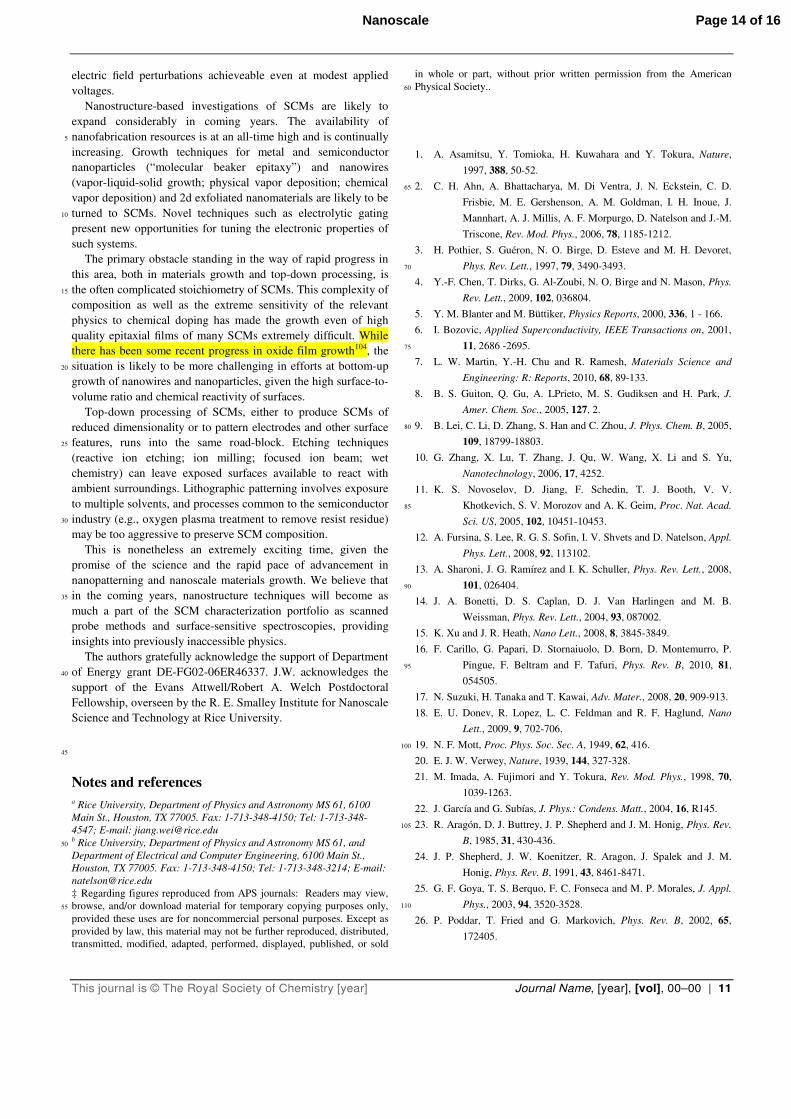
Spatial confinement approaching the nanoscale also allows
detailed studies of phase coherence and the effects of magnetic
fields in the high-Tc cuprates. Two recent investigations have 20
looked at magnetoresistance oscillations in small rings, either
individually16 or in a linked 2D array95. In both cases, working
with nanoscale rings and wire widths allows the investigations to
take place at comparatively large field scales (corresponding with
threading quanta of magnetic flux, h/2e, through the ring). The 25
physics examined was the Little-Parks effect96, 97, the oscillation
of Tc of the ring structure periodic in the flux, with period h/2e.
This periodicity arises because of circulating persistent currents
required to quantize the flux through the ring.
The single-ring investigations in YBCO16 show features 30
indicating beating of different, close field periodicities,
interpreted as a signature of nonuniform vorticity within the
finite-width superconducting ring (see Fig. 12a). In contrast, the
array measurements95 (see Fig. 12b) in La1.84Sr0.16CuO4 show
magnetoresistance oscillations two orders of magnitude larger 35
than those expected for Little-Parks. The authors are able to
explain both the magnitude and the temperature dependence of
this effect through interactions between the persistent currents
and vortices/antivortices in the superconductor.
Because the cuprates are inherently layered compounds, there 40
have also been investigations trying to manipulate individual,
exfoliated sheets of some of these materials, particularly those
related to the bismuth strontium copper oxide family11, 98.
However, this approach has not yet met with success, in terms of
producing structures that exhibit superconductivity. 45
Fig. 12 Nanoscale multiply connected high temperature superconductors.
(a) An example of a single nanoscale YBCO ring patterned for
investigating the Little-Parks effect. Adapted with permission from F. 50
Carillo et al., Phys. Rev. B 81, 054505 (2010). Copyright 2010 by the
American Physical Society. (b) An array of cuprate superconductor rings
observed to exhibit magnetoresistance oscillations much larger than those
expected from the simple Little-Parks effect. Adapted with permission
from I. Sochnikov et al., Phys. Rev. B 82, 094513 (2010). Copyright 55
2010 by the American Physical Society.
In contrast, field effect gating has been attempted numerous
times as an attempt to tune the superconducting properties of
these strongly correlated materials without chemical doping. An
extensive review99 highlights the challenge in this work. 60
Significant modulation of the correlated state properties requires
changing the charge distribution at a level approaching a charge
carrier per unit cell. This gated charge density is extremely
difficult to achieve with conventional gate dielectrics because of
the limits of breakdown electric field and relative dielectric 65
constant. The most successful approach in the cuprates has
employed a ferroelectric as the gate insulator100. With a 2 nm
thick GdBa2Cu3O7−x channel layer having Tc ≈ 50 K, the
ferroelectric remnant polarization of 10 µC/cm2 was sufficent to
modulate Tc by several Kelvin. More recently, electrolytic gating 70
has been put forward as a means of achieving similar surface
carrier densities101, with one report of its use in a cuprate
structure102 to shift Tc by tens of percent. More recently103,
electrolytic gating in a single-unit-cell-thick La2-xSrxCuO4 layer
has cleanly modulated the material from the insulating regime 75
through into superconductivity with Tc ~ 40 K.
Conclusions
The physics of strongly correlated materials remains rich,
fascinating, and a challenge to experimentalists as well as 80
theorists. Only recently have the hard-won nanofabrication skills
acquired as a result of decades of semiconductor research been
applied to these material systems. As has been described above,
nanostructure experiments that directly incorporate SCMs are on
the rise, and have much to reveal about the underlying physics of 85
these materials. Complementing scanned probe experiments,
nanodevice methods can examine intrinsic and extrinsic
inhomogeneities on their characteristic length scales.
Nanostructures can throw the effects of contacts, comparatively
unstudied and often actively avoided, into sharp relief, and 90
analysis of contact effects can further illuminate the bulk physics.
Nanostructures also enable nonequilibrium studies, with large
Page 13 of 16 Nanoscale
This journal is © The Royal Society of Chemistry [year] Journal Name, [year], [vol], 00–00 | 11
electric field perturbations achieveable even at modest applied
voltages.
Nanostructure-based investigations of SCMs are likely to
expand considerably in coming years. The availability of
nanofabrication resources is at an all-time high and is continually 5
increasing. Growth techniques for metal and semiconductor
nanoparticles (“molecular beaker epitaxy”) and nanowires
(vapor-liquid-solid growth; physical vapor deposition; chemical
vapor deposition) and 2d exfoliated nanomaterials are likely to be
turned to SCMs. Novel techniques such as electrolytic gating 10
present new opportunities for tuning the electronic properties of
such systems.
The primary obstacle standing in the way of rapid progress in
this area, both in materials growth and top-down processing, is
the often complicated stoichiometry of SCMs. This complexity of 15
composition as well as the extreme sensitivity of the relevant
physics to chemical doping has made the growth even of high
quality epitaxial films of many SCMs extremely difficult. While
there has been some recent progress in oxide film growth104, the
situation is likely to be more challenging in efforts at bottom-up 20
growth of nanowires and nanoparticles, given the high surface-to-
volume ratio and chemical reactivity of surfaces.
Top-down processing of SCMs, either to produce SCMs of
reduced dimensionality or to pattern electrodes and other surface
features, runs into the same road-block. Etching techniques 25
(reactive ion etching; ion milling; focused ion beam; wet
chemistry) can leave exposed surfaces available to react with
ambient surroundings. Lithographic patterning involves exposure
to multiple solvents, and processes common to the semiconductor
industry (e.g., oxygen plasma treatment to remove resist residue) 30
may be too aggressive to preserve SCM composition.
This is nonetheless an extremely exciting time, given the
promise of the science and the rapid pace of advancement in
nanopatterning and nanoscale materials growth. We believe that
in the coming years, nanostructure techniques will become as 35
much a part of the SCM characterization portfolio as scanned
probe methods and surface-sensitive spectroscopies, providing
insights into previously inaccessible physics.
The authors gratefully acknowledge the support of Department
of Energy grant DE-FG02-06ER46337. J.W. acknowledges the 40
support of the Evans Attwell/Robert A. Welch Postdoctoral
Fellowship, overseen by the R. E. Smalley Institute for Nanoscale
Science and Technology at Rice University.
45
Notes and references
a Rice University, Department of Physics and Astronomy MS 61, 6100
Main St., Houston, TX 77005. Fax: 1-713-348-4150; Tel: 1-713-348-
4547; E-mail: [email protected] b Rice University, Department of Physics and Astronomy MS 61, and 50
Department of Electrical and Computer Engineering, 6100 Main St.,
Houston, TX 77005. Fax: 1-713-348-4150; Tel: 1-713-348-3214; E-mail:
‡ Regarding figures reproduced from APS journals: Readers may view,
browse, and/or download material for temporary copying purposes only, 55
provided these uses are for noncommercial personal purposes. Except as
provided by law, this material may not be further reproduced, distributed,
transmitted, modified, adapted, performed, displayed, published, or sold
in whole or part, without prior written permission from the American
Physical Society.. 60
1. A. Asamitsu, Y. Tomioka, H. Kuwahara and Y. Tokura, Nature,
1997, 388, 50-52.
2. C. H. Ahn, A. Bhattacharya, M. Di Ventra, J. N. Eckstein, C. D. 65
Frisbie, M. E. Gershenson, A. M. Goldman, I. H. Inoue, J.
Mannhart, A. J. Millis, A. F. Morpurgo, D. Natelson and J.-M.
Triscone, Rev. Mod. Phys., 2006, 78, 1185-1212.
3. H. Pothier, S. Guéron, N. O. Birge, D. Esteve and M. H. Devoret,
Phys. Rev. Lett., 1997, 79, 3490-3493. 70
4. Y.-F. Chen, T. Dirks, G. Al-Zoubi, N. O. Birge and N. Mason, Phys.
Rev. Lett., 2009, 102, 036804.
5. Y. M. Blanter and M. Büttiker, Physics Reports, 2000, 336, 1 - 166.
6. I. Bozovic, Applied Superconductivity, IEEE Transactions on, 2001,
11, 2686 -2695. 75
7. L. W. Martin, Y.-H. Chu and R. Ramesh, Materials Science and
Engineering: R: Reports, 2010, 68, 89-133.
8. B. S. Guiton, Q. Gu, A. LPrieto, M. S. Gudiksen and H. Park, J.
Amer. Chem. Soc., 2005, 127, 2.
9. B. Lei, C. Li, D. Zhang, S. Han and C. Zhou, J. Phys. Chem. B, 2005, 80
109, 18799-18803.
10. G. Zhang, X. Lu, T. Zhang, J. Qu, W. Wang, X. Li and S. Yu,
Nanotechnology, 2006, 17, 4252.
11. K. S. Novoselov, D. Jiang, F. Schedin, T. J. Booth, V. V.
Khotkevich, S. V. Morozov and A. K. Geim, Proc. Nat. Acad. 85
Sci. US, 2005, 102, 10451-10453.
12. A. Fursina, S. Lee, R. G. S. Sofin, I. V. Shvets and D. Natelson, Appl.
Phys. Lett., 2008, 92, 113102.
13. A. Sharoni, J. G. Ramírez and I. K. Schuller, Phys. Rev. Lett., 2008,
101, 026404. 90
14. J. A. Bonetti, D. S. Caplan, D. J. Van Harlingen and M. B.
Weissman, Phys. Rev. Lett., 2004, 93, 087002.
15. K. Xu and J. R. Heath, Nano Lett., 2008, 8, 3845-3849.
16. F. Carillo, G. Papari, D. Stornaiuolo, D. Born, D. Montemurro, P.
Pingue, F. Beltram and F. Tafuri, Phys. Rev. B, 2010, 81, 95
054505.
17. N. Suzuki, H. Tanaka and T. Kawai, Adv. Mater., 2008, 20, 909-913.
18. E. U. Donev, R. Lopez, L. C. Feldman and R. F. Haglund, Nano
Lett., 2009, 9, 702-706.
19. N. F. Mott, Proc. Phys. Soc. Sec. A, 1949, 62, 416. 100
20. E. J. W. Verwey, Nature, 1939, 144, 327-328.
21. M. Imada, A. Fujimori and Y. Tokura, Rev. Mod. Phys., 1998, 70,
1039-1263.
22. J. García and G. Subías, J. Phys.: Condens. Matt., 2004, 16, R145.
23. R. Aragón, D. J. Buttrey, J. P. Shepherd and J. M. Honig, Phys. Rev. 105
B, 1985, 31, 430-436.
24. J. P. Shepherd, J. W. Koenitzer, R. Aragon, J. Spalek and J. M.
Honig, Phys. Rev. B, 1991, 43, 8461-8471.
25. G. F. Goya, T. S. Berquo, F. C. Fonseca and M. P. Morales, J. Appl.
Phys., 2003, 94, 3520-3528. 110
26. P. Poddar, T. Fried and G. Markovich, Phys. Rev. B, 2002, 65,
172405.
Page 14 of 16Nanoscale
12 | Journal Name, [year], [vol], 00–00 This journal is © The Royal Society of Chemistry [year]
27. S. Lee, A. Fursina, J. T. Mayo, C. T. Yavuz, V. L. Colvin, R. G. S.
Sofin, I. V. Shvets and D. Natelson, Nature Mater., 2007, 7,
130-133.
28. R. Waser and M. Aono, Nature Mater., 2007, 6, 833-840.
29. A. Sawa, Materials Today, 2008, 11, 28 - 36. 5
30. T. Oka and H. Aoki, Phys. Rev. Lett., 2005, 95, 137601.
31. N. Sugimoto, S. Onoda and N. Nagaosa, Phys. Rev. B, 2008, 78,
155104.
32. A. A. Fursina, R. G. S. Sofin, I. V. Shvets and D. Natelson, Phys.
Rev. B, 2009, 79, 245131. 10
33. J. S. Morris and D. Natelson, unpublished, 2011.
34. A. A. Fursina, R. G. S. Sofin, I. V. Shvets and D. Natelson, Phys.
Rev. B, 2010, 82, 245112.
35. A. A. Fursina, R. G. S. Sofin, I. V. Shvets and D. Natelson, Phys.
Rev. B, 2010, 81, 045123. 15
36. Y. Shen, M. W. Klein, D. B. Jacobs, J. Campbell Scott and G. G.
Malliaras, Phys. Rev. Lett., 2001, 86, 3867-3870.
37. B. H. Hamadani and D. Natelson, Appl. Phys. Lett., 2004, 84, 443-
445.
38. J. C. Scott, J. Vac. Sci. Tech. A, 2003, 21, 521-531. 20
39. F. Walz, J. Phys.: Condens. Matt., 2002, 14, R285.
40. F. J. Morin, Phys. Rev. Lett., 1959, 3, 34.
41. H. W. Verleur, A. S. Barker and C. N. Berglund, Phys. Rev., 1968,
172, 788.
42. J. Wei, Z. Wang, W. Chen and D. H. Cobden, Nat Nano, 2009, 4, 25
420-424.
43. T. M. Rice, H. Launois and J. P. Pouget, Phys. Rev. Lett., 1994, 73,
3042.
44. R. M. Wentzcovitch, W. W. Schulz and P. B. Allen, Phys. Rev. Lett.,
1994, 72, 3389. 30
45. C. N. Berglund and H. J. Guggenheim, Phys. Rev., 1969, 185, 1022.
46. P. B. Allen, R. M. Wentzcovitch, W. W. Schulz and P. C. Canfield,
Phys. Rev. B, 1993, 48, 4359-4363.
47. M. M. Qazilbash, K. S. Burch, D. Whisler, D. Shrekenhamer, B. G.
Chae, H. T. Kim and D. N. Basov, Phys. Rev. B, 2006, 74, 35
205118.
48. V. Eyert, Annalen Der Physik, 2002, 11, 650-702.
49. J. P. Pouget, H. Launois, J. P. Dhaenens, P. Merenda and T. M. Rice,
Phys. Rev. Lett., 1975, 35, 873-875.
50. M. Marezio, B. Mcwhan, P. D. Dernier and J. P. Remeika, Phys. Rev. 40
B, 1972, 5, 2541-&.
51. D. J. Hilton, R. P. Prasankumar, S. Fourmaux, A. Cavalleri, D.
Brassard, M. A. El Khakani, J. C. Kieffer, A. J. Taylor and R.
D. Averitt, Phys. Rev. Lett., 2007, 99, 226401.
52. P. Baum, D. S. Yang and A. H. Zewail, Science, 2007, 318, 788-792. 45
53. M. M. Qazilbash, M. Brehm, B. G. Chae, P. C. Ho, G. O. Andreev,
B. J. Kim, S. J. Yun, A. V. Balatsky, M. B. Maple, F.
Keilmann, H. T. Kim and D. N. Basov, Science, 2007, 318,
1750-1753.
54. F. Chudnovskiy, S. Luryi and B. Spivak, in Future Trends in 50
Microelectronics: The Nano Millennium, Wiley-IEEE Press,
2002.
55. H. Jerominek, F. Picard and D. Vincent, Optical Engineering, 1993,
32, 2092-2099.
56. R. Lopez, J. Richard F. Haglund, L. C. Feldman and a. T. E. H. Lynn 55
A. Boatner, Proceedings SPIE 2006, 6118.
57. A. Cavalleri, T. Dekorsy, H. H. W. Chong, J. C. Kieffer and R. W.
Schoenlein, Phys. Rev. B, 2004, 70, 161102(R).
58. M. M. Qazilbash, M. Brehm, B.-G. Chae, P.-C. Ho, G. O. Andreev,
B.-J. Kim, S. J. Yun, A. V. Balatsky, M. B. Maple, F. 60
Keilmann, H.-T. Kim and D. N. Basov, Science, 2007, 318,
1750.
59. G. Stefanovich and et al., J. Phys.: Condens. Matt., 2000, 12, 8837.
60. B.-G. Chae, H.-T. Kim, D.-H. Youn and K.-Y. Kang, Physica B:
Condensed Matter, 2005, 369, 76-80. 65
61. D. Ruzmetov, D. Heiman, B. B. Claflin, V. Narayanamurti and S.
Ramanathan, Phys. Rev. B, 2009, 79, 153107.
62. J. Cao, E. Ertekin and W. F. V. Srinivasan, S. Huang, H. Zheng, J.
W. L. Yim, D. R. Khanal, D. F. Ogletree, J. C. Grossman, and
J. Wu,, Nature Nanotechnology, 2009, 4, 732-737. 70
63. J. I. Sohn, H. J. Joo, D. Ahn, H. H. Lee, A. E. Porter, K. Kim, D. J.
Kang and M. E. Welland, Nano Letters, 2009, 9, 3392-3397.
64. A. C. Jones, S. Berweger, J. Wei, D. Cobden and M. B. Raschke,
Nano Lett., 2010, 10, 1574-1581.
65. M. B. Salamon and M. Jaime, Rev. Mod. Phys., 2001, 73, 583-628. 75
66. A. P. Ramirez, J. Phys.: Condens. Matt., 1997, 9, 8171.
67. E. Dagotto, Science, 2005, 309, 257-262.
68. E. Dagotto, T. Hotta and A. Moreo, Physics Reports, 2001, 344, 1-
153.
69. M. Fäth, S. Freisem, A. A. Menovsky, Y. Tomioka, J. Aarts and J. A. 80
Mydosh, Science, 1999, 285, 1540-1542.
70. C. Renner, G. Aeppli, B.-G. Kim, Y.-A. Soh and S.-W. Cheong,
Nature, 2002, 416, 518-521.
71. Y. Yanagisawa, H. Tanaka, T. Kawai and L. Pellegrino, Appl. Phys.
Lett., 2006, 89, 253121. 85
72. H.-Y. Zhai, J. X. Ma, D. T. Gillaspie, X. G. Zhang, T. Z. Ward, E. W.
Plummer and J. Shen, Phys. Rev. Lett., 2006, 97, 167201.
73. M. Uehara, S. Mori, C. H. Chen and S.-W. Cheong, Nature, 1999,
399, 560-563.
74. L. Zhang, C. Israel, A. Biswas, R. L. Greene and A. de Lozanne, 90
Science, 2002, 298, 805-807.
75. K. K. Gomes, A. N. Pasupathy, A. Pushp, S. Ono, Y. Ando and A.
Yazdani, Nature, 2007, 447, 569-572.
76. T. Z. Ward, S. Liang, K. Fuchigami, L. F. Yin, E. Dagotto, E. W.
Plummer and J. Shen, Phys. Rev. Lett., 2008, 100, 247204. 95
77. T. Nakajima, T. Tsuchiya, Y. Ueda and T. Kumagai, Phys. Rev. B,
2009, 80, 020401.
78. T. Z. Ward, X. G. Zhang, L. F. Yin, X. Q. Zhang, M. Liu, P. C.
Snijders, S. Jesse, E. W. Plummer, Z. H. Cheng, E. Dagotto
and J. Shen, Phys. Rev. Lett., 2009, 102, 087201. 100
79. G. Singh-Bhalla, S. Selcuk, T. Dhakal, A. Biswas and A. F. Hebard,
Phys. Rev. Lett., 2009, 102, 077205.
80. E. Abrahams, P. W. Anderson, D. C. Licciardello and T. V.
Ramakrishnan, Phys. Rev. Lett., 1979, 42, 673-676.
81. G. Singh-Bhalla, A. Biswas and A. F. Hebard, Phys. Rev. B, 2009, 105
80, 144410.
82. T. Wu, S. B. Ogale, J. E. Garrison, B. Nagaraj, A. Biswas, Z. Chen,
R. L. Greene, R. Ramesh, T. Venkatesan and A. J. Millis,
Phys. Rev. Lett., 2001, 86, 5998-6001.
83. P. Mohanty, J. Y. T. Wei, V. Ananth, P. Morales and W. Skocpol, 110
Physica C: Superconductivity, 2004, 408-410, 666 - 669.
Page 15 of 16 Nanoscale
This journal is © The Royal Society of Chemistry [year] Journal Name, [year], [vol], 00–00 | 13
84. J. Lee, K. Fujita, A. R. Schmidt, C. K. Kim, H. Eisaki, S. Uchida and
J. C. Davis, Science, 2009, 325, 1099-1103.
85. S. A. Kivelson, I. P. Bindloss, E. Fradkin, V. Oganesyan, J. M.
Tranquada, A. Kapitulnik and C. Howald, Rev. Mod. Phys.,
2003, 75, 1201-1241. 5
86. P. Abbamonte, A. Rusydi, S. Smadici, G. D. Gu, G. A. Sawatzky and
D. L. Feng, Nature Physics, 2005, 1, 155-158.
87. K. McElroy, J. Lee, J. Slezak, D. Lee, H. Eisaki, S. Uchida and J.
Davis, Science, 2005, 309, 1048-1052.
88. Z. Ma, R. C. Taber, L. W. Lombardo, A. Kapitulnik, M. R. Beasley, 10
P. Merchant, C. B. Eom, S. Y. Hou and J. M. Phillips, Phys.
Rev. Lett., 1993, 71, 781-784.
89. H. Jiang, Y. Huang, H. How, S. Zhang, C. Vittoria, A. Widom, D. B.
Chrisey, J. S. Horwitz and R. Lee, Phys. Rev. Lett., 1991, 66,
1785-1788. 15
90. P. Larsson, B. Nilsson and Z. G. Ivanov, J. Vac. Sci. Tech. B, 2000,
18, 25-31.
91. P. Mikheenko, X. Deng, S. Gildert, M. S. Colclough, R. A. Smith, C.
M. Muirhead, P. D. Prewett and J. Teng, Phys. Rev. B, 2005,
72, 174506. 20
92. C. N. Lau, N. Markovic, M. Bockrath, A. Bezryadin and M.
Tinkham, Phys. Rev. Lett., 2001, 8721, 217003.
93. N. A. Melosh, A. Boukai, F. Diana, B. Gerardot, A. Badolato, P. M.
Petroff and J. R. Heath, Science, 2003, 300, 112-115.
94. D. S. Caplan, V. Orlyanchik, M. B. Weissman, D. J. Van Harlingen, 25
E. H. Fradkin, M. J. Hinton and T. R. Lemberger, Phys. Rev.
Lett., 2010, 104, 177001.
95. I. Sochnikov, A. Shaulov, Y. Yeshurun, G. Logvenov and I. Bozovic,
Phys. Rev. B, 2010, 82, 094513.
96. W. A. Little and R. D. Parks, Phys. Rev. Lett., 1962, 9, 9. 30
97. R. D. Parks and W. A. Little, Phys. Rev., 1964, 133, A97.
98. L. J. Sandilands, J. X. Shen, G. M. Chugunov, S. Y. F. Zhao, S. Ono,
Y. Ando and K. S. Burch, Phys. Rev. B, 2010, 82, 064503.
99. C. H. Ahn, J.-M. Triscone and J. Mannhart, Nature, 2003, 424, 1015-
1018. 35
100. C. H. Ahn, S. Gariglio, P. Paruch, T. Tybell, L. Antognazza and J.-
M. Triscone, Science, 1999, 284, 1152-1155.
101. J. T. Ye, S. Inoue, K. Kobayashi, Y. Kasahara, H. T. Yuan, H.
Shimotani and Y. Iwasa, Nature Mater., 2010, 9, 125-128.
102. A. S. Dhoot, S. C. Wimbush, T. Benseman, J. L. MacManus-Driscoll, 40
J. R. Cooper and R. H. Friend, Adv. Mater., 2010, 22, 2529-
2533.
103. A. T. Bollinger, G. Dubuis, J. Yoon, D. Pavuna, J. Misewich and I.
Bozovic, Nature, 472, 458-460.
104. J. Son, J. Cagnon and S. Stemmer, Appl. Phys. Lett., 2009, 94, 45
062903.
Page 16 of 16Nanoscale
Related Documents