Nanoscopic Pd Line Arrays Using Nanocontact Printed Dendrimers Se Gyu Jang, ² Dae-Geun Choi, ‡ Sarah Kim, ² Jun-ho Jeong, ‡ Eung-sug Lee, ‡ and Seung-Man Yang* ,² Department of Chemical and Biomolecular Engineering, Korea AdVanced Institute of Science and Technology, 373-1 Guseong-dong, Yuseong-gu, Daejeon 305-701 Korea, and Nano-Mechanical Systems Research Center, Korea Institute of Machinery and Materials, 171 Jang-dong, Yuseong-gu, Daejeon, 305-343, Korea ReceiVed September 14, 2005. In Final Form: January 15, 2006 High-density Pd line arrays with 55 nm line-width were obtained using nanocontact-printed dendrimer monolayers. Elastomeric PDMS stamps for nanocontact printing were replicated from silicon master molds which were fabricated by UV nanoimprinting in combination with reactive ion etching. The fabrication method effectively controlled the aspect ratios of high-density lines for resolving the problems encountered in both replicating silicon masters to PDMS stamps and printing with the replicated PDMS stamps. Using the PDMS nanostamp with an optimized aspect ratio, a self-assembled monolayer of dendrimer was patterned on a Pd film via nanocontact printing, which was facilitated by the strong interaction between Pd and amine groups of the dendrimer. The patterned self-assembled monolayer was used as an etch-resist mask against the wet etchant of Pd, leaving behind a high-density Pd line array over large areas. The resulting functional Pd nanopattern is of practical significance in microelectronics and bio- or gas-sensing devices. Introduction The fabrication of nanoscopic patterns with sub-100-nm feature sizes has been a demanding issue for a decade. Although advanced lithographic tools with e-beam, dip-pen, and focused ion beam have been investigated intensively to create sub-50-nm patterns, 1 these methods have not been able to satisfy the throughput requirements for industrial use until now because they require very expensive and complex equipment, as well as a long process time. Microcontact printing (μCP) 2 has been known as a simple, fast, and inexpensive method to fabricate micrometer-scale patterns using self-assembled monolayers (SAMs) printed with poly(dimethylsiloxane) (PDMS) stamps. Microcontact printed SAM patterns have been used as ultrathin resists in selective wet etching 3 and as templates for fabricating polymeric multilayers and three-dimensional structures of metals and other materials. 4-7 However, there have been two main limitations for extending this simple μCP to nanofeature scales; namely, difficulty in preparing nanoscale stamp materials with high feature density and suppressing diffusion of SAM inks. 8 For nanoscopic contact printing (henceforth, NCP), we have to consider a few requirements for the properties of stamp materials. First, a stamp should be mechanically strong, so that it would not be torn when it is peeled from the master molds with high feature density. Second, the stamp materials should have a sufficiently high modulus that shape deformation such as the sagging, buckling, and widening of the contact area caused by pressure would not occur. 9 Third, they should be wettable with SAM inks and proper for conformal contact with a substrate. To satisfy these requirements, composite stamps 10 of stiff hard- PDMS (h-PDMS) supported by flexible soft PDMS have been used frequently for sub-100-nm patterns because of their good mechanical property and replication performance, as well as ease of fabrication. However, the replication of the composite stamp is still difficult when the feature size and pattern period are decreased to sub-100-nm scales with high aspect ratios due to mechanical failure. This is especially true for high-density nanopatterns over large surface areas. The aspect ratio should be large enough for height contrast and also small enough to avoid the tearing problem when the PDMS replica is peeled from the high-density master, and therefore, it is required to optimize the aspect ratio of the master for proper subsequent replications. For high-resolution pattern formation by NCP, SAM ink materials should not diffuse prior to the anchoring with a substrate. Recently, dendrimers (or hyperbranched polymers) have been used in the diffusion-controlled NCP on silicon oxide substrate * To whom correspondence should be addressed. E-mail: smyang@ kaist.ac.kr. Tel: +82-42-869-3922. Fax: +82-42-869-5962. ² Korea Advanced Institute of Science and Technology. ‡ Korea Institute of Machinery and Materials. (1) (a) Landis, S.; Rodmacq, B.; Dieny, B. Phys. ReV.B 2000, 62, 12271. (b) Piner, R. D.; Zhu, J.; Xu, F.; Hong, S.; Mirkin, C. A. Science 1999, 283, 661. (c) Rettner, C. T.; Anders, S.; Thomson, T.; Albrecht, M.; Best, M. E.; Terris, B. D. IEEE Trans. Magn. 2002, 38, 1725. (2) Kumar, A.; Whitesides, G. M. Appl. Phys. Lett. 1993, 63, 200. (3) (a) Xia, Y.; Zhao, X.-M.; Whitesides, G. M. Microelectron. Eng. 1996, 32, 255. (b) Xia, Y.; Zhao, X.-M.; Kim, E.; Whitesides, G. M. Chem. Mater. 1995, 7, 2332. (c) Love, J. C.; Wolfe, D. B.; Chabinyc, M. L.; Paul, K. E.; Whitesides, G. M. J. Am. Chem. Soc. 2002, 124, 1576. (4) (a) Kim, E.; Whitesides, G. M.; Lee, L. K.; Smith, S. P.; Prentiss, M. AdV. Mater. 1996, 8, 139. (b) Zhang, H.-L.; Bucknall, D. G.; Dupuis, A. Nano Lett. 2004, 4, 1513. (5) Huck, W. T. S.; Yan, L.; Stroock, A.; Haag, R.; Whitesides, G. M. Langmuir 1999, 15, 6862. (6) Rogers, J. A.; Jackman, R. J.; Whitesides, G. M. AdV. Mater. 1997, 9, 475. (7) (a) Gorman, C. B.; Biebuyck, H. A.; Whitesides, G. M. Chem. Mater. 1995, 7, 526. (b) Yang, H.; Coombs, N.; Ozin, G. A. AdV. Mater. 1997, 9, 811. (c) Zhou, F.; Chen, M.; Liu, W.; Liu, J.; Liu, Z.; Mu, Z. AdV. Mater. 2003, 15, 1367. (d) Park, M. H.; Jang, Y. J.; Sung-Suh, H. M.; Sung, M. M. Langmuir 2004, 20, 2257. (8) (a) Li, H.-W.; Muir, B. V. O.; Fichet, G.; Huck, W. T. S. Langmuir 2003, 19, 1963. (b) Li, H.-W.; Kang, D-. J.; Blamire, M. G.; Huck, W. T. S. Nano. Lett. 2002, 2, 347. (9) (a) Delamarche, E.; Schmid, H.; Michel, B.; Biebuyck, H. AdV. Mater. 1997, 9, 741. (b) Rogers, J. A.; Paul, K. E.; Whitesides, G. M. J. Vac. Sci. Technol. B 1998, 16, 88. (c) Hui, C. Y.; Jagota, A.; Lin, Y. Y.; Kramer, E. J. Langmuir 2002, 18, 1394. (d) Sharp, K. G.; Bloackman, G. S.; Glassmaker, N. J.; Jagota, A.; Hui, C.-Y. Langmuir 2004, 20, 6430. (10) Odom, T. W.; Love, J. C.; Wolfe, D. B.; Paul, K. E.; Whitesides, G. M. Langmuir 2002, 18, 5314. 3326 Langmuir 2006, 22, 3326-3331 10.1021/la0525170 CCC: $33.50 © 2006 American Chemical Society Published on Web 02/23/2006

Welcome message from author
This document is posted to help you gain knowledge. Please leave a comment to let me know what you think about it! Share it to your friends and learn new things together.
Transcript
Nanoscopic Pd Line Arrays Using Nanocontact Printed Dendrimers
Se Gyu Jang,† Dae-Geun Choi,‡ Sarah Kim,† Jun-ho Jeong,‡ Eung-sug Lee,‡ andSeung-Man Yang*,†
Department of Chemical and Biomolecular Engineering, Korea AdVanced Institute of Science andTechnology, 373-1 Guseong-dong, Yuseong-gu, Daejeon 305-701 Korea, and Nano-Mechanical Systems
Research Center, Korea Institute of Machinery and Materials, 171 Jang-dong, Yuseong-gu,Daejeon, 305-343, Korea
ReceiVed September 14, 2005. In Final Form: January 15, 2006
High-density Pd line arrays with 55 nm line-width were obtained using nanocontact-printed dendrimer monolayers.Elastomeric PDMS stamps for nanocontact printing were replicated from silicon master molds which were fabricatedby UV nanoimprinting in combination with reactive ion etching. The fabrication method effectively controlled theaspect ratios of high-density lines for resolving the problems encountered in both replicating silicon masters to PDMSstamps and printing with the replicated PDMS stamps. Using the PDMS nanostamp with an optimized aspect ratio,a self-assembled monolayer of dendrimer was patterned on a Pd film via nanocontact printing, which was facilitatedby the strong interaction between Pd and amine groups of the dendrimer. The patterned self-assembled monolayerwas used as an etch-resist mask against the wet etchant of Pd, leaving behind a high-density Pd line array over largeareas. The resulting functional Pd nanopattern is of practical significance in microelectronics and bio- or gas-sensingdevices.
Introduction
The fabrication of nanoscopic patterns with sub-100-nm featuresizes has been a demanding issue for a decade. Although advancedlithographic tools with e-beam, dip-pen, and focused ion beamhave been investigated intensively to create sub-50-nm patterns,1
these methods have not been able to satisfy the throughputrequirements for industrial use until now because they requirevery expensive and complex equipment, as well as a long processtime.
Microcontact printing (µCP)2 has been known as a simple,fast, and inexpensive method to fabricate micrometer-scalepatterns using self-assembled monolayers (SAMs) printed withpoly(dimethylsiloxane) (PDMS) stamps. Microcontact printedSAM patterns have been used as ultrathin resists in selective wetetching3 and as templates for fabricating polymeric multilayersand three-dimensional structures of metals and other materials.4-7
However, there have been two main limitations for extendingthis simpleµCP to nanofeature scales; namely, difficulty in
preparing nanoscale stamp materials with high feature densityand suppressing diffusion of SAM inks.8
For nanoscopic contact printing (henceforth, NCP), we haveto consider a few requirements for the properties of stampmaterials. First, a stamp should be mechanically strong, so thatit would not be torn when it is peeled from the master molds withhigh feature density. Second, the stamp materials should havea sufficiently high modulus that shape deformation such as thesagging, buckling, and widening of the contact area caused bypressure would not occur.9 Third, they should be wettable withSAM inks and proper for conformal contact with a substrate. Tosatisfy these requirements, composite stamps10 of stiff hard-PDMS (h-PDMS) supported by flexible soft PDMS have beenused frequently for sub-100-nm patterns because of their goodmechanical property and replication performance, as well asease of fabrication. However, the replication of the compositestamp is still difficult when the feature size and pattern periodare decreased to sub-100-nm scales with high aspect ratios dueto mechanical failure. This is especially true for high-densitynanopatterns over large surface areas. The aspect ratio shouldbe large enough for height contrast and also small enough toavoid the tearing problem when the PDMS replica is peeledfrom the high-density master, and therefore, it is required tooptimize the aspect ratio of the master for proper subsequentreplications.
For high-resolution pattern formation by NCP, SAM inkmaterials should not diffuse prior to the anchoring with a substrate.Recently, dendrimers (or hyperbranched polymers) have beenused in the diffusion-controlled NCP on silicon oxide substrate
* To whom correspondence should be addressed. E-mail: [email protected]. Tel:+82-42-869-3922. Fax:+82-42-869-5962.
† Korea Advanced Institute of Science and Technology.‡ Korea Institute of Machinery and Materials.(1) (a) Landis, S.; Rodmacq, B.; Dieny, B. Phys. ReV. B 2000, 62, 12271. (b)
Piner, R. D.; Zhu, J.; Xu, F.; Hong, S.; Mirkin, C. A.Science1999, 283, 661.(c) Rettner, C. T.; Anders, S.; Thomson, T.; Albrecht, M.; Best, M. E.; Terris,B. D. IEEE Trans. Magn.2002, 38, 1725.
(2) Kumar, A.; Whitesides, G. M.Appl. Phys. Lett. 1993, 63, 200.(3) (a) Xia, Y.; Zhao, X.-M.; Whitesides, G. M.Microelectron. Eng.1996, 32,
255. (b) Xia, Y.; Zhao, X.-M.; Kim, E.; Whitesides, G. M.Chem. Mater.1995,7, 2332. (c) Love, J. C.; Wolfe, D. B.; Chabinyc, M. L.; Paul, K. E.; Whitesides,G. M. J. Am. Chem. Soc.2002, 124, 1576.
(4) (a) Kim, E.; Whitesides, G. M.; Lee, L. K.; Smith, S. P.; Prentiss, M.AdV.Mater. 1996, 8, 139. (b) Zhang, H.-L.; Bucknall, D. G.; Dupuis, A.Nano Lett.2004, 4, 1513.
(5) Huck, W. T. S.; Yan, L.; Stroock, A.; Haag, R.; Whitesides, G. M.Langmuir1999, 15, 6862.
(6) Rogers, J. A.; Jackman, R. J.; Whitesides, G. M.AdV. Mater. 1997, 9, 475.(7) (a) Gorman, C. B.; Biebuyck, H. A.; Whitesides, G. M.Chem. Mater.
1995, 7, 526. (b) Yang, H.; Coombs, N.; Ozin, G. A.AdV. Mater.1997, 9, 811.(c) Zhou, F.; Chen, M.; Liu, W.; Liu, J.; Liu, Z.; Mu, Z.AdV. Mater. 2003, 15,1367. (d) Park, M. H.; Jang, Y. J.; Sung-Suh, H. M.; Sung, M. M.Langmuir2004,20, 2257.
(8) (a) Li, H.-W.; Muir, B. V. O.; Fichet, G.; Huck, W. T. S.Langmuir2003,19, 1963. (b) Li, H.-W.; Kang, D-. J.; Blamire, M. G.; Huck, W. T. S.Nano. Lett.2002, 2, 347.
(9) (a) Delamarche, E.; Schmid, H.; Michel, B.; Biebuyck, H.AdV. Mater.1997, 9, 741. (b) Rogers, J. A.; Paul, K. E.; Whitesides, G. M.J. Vac. Sci. Technol.B 1998, 16, 88. (c) Hui, C. Y.; Jagota, A.; Lin, Y. Y.; Kramer, E. J.Langmuir2002, 18, 1394. (d) Sharp, K. G.; Bloackman, G. S.; Glassmaker, N. J.; Jagota,A.; Hui, C.-Y. Langmuir2004, 20, 6430.
(10) Odom, T. W.; Love, J. C.; Wolfe, D. B.; Paul, K. E.; Whitesides, G. M.Langmuir2002, 18, 5314.
3326 Langmuir2006,22, 3326-3331
10.1021/la0525170 CCC: $33.50 © 2006 American Chemical SocietyPublished on Web 02/23/2006
for biological applications because they are less diffusible andcan be transferred to the silicon oxide surface.8 Most researchon dendrimer SAMs has focused mainly on the adsorption ofdendrimers on the oxide surface with a primary interactionbetween amine and hydroxyl groups.11 For metallic substrates,Tokuhisa et al. demonstrated the adsorption of dendrimers andalkanethiol-mixed dendrimers on gold surface.12 Their resultsshowed that functional metallic nanostructures can be fabricatedusing patterned dendrimer SAMs as an etch-resist mask againstthe wet etching.
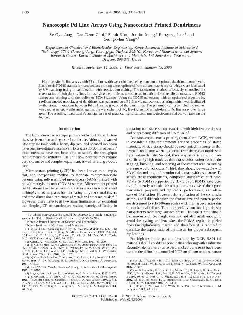
In this article, we report a novel method for fabricating ahigh-density Pd line array with 55-nm line-width over large areasusing NCP of dendrimers on a Pd substrate. First, polymericpatterns were formed using UV nanoimprint lithography (UV-NIL).13 Then, the imprinted polymeric patterns were transferredto a silicon (Si) wafer by reactive ion etching (RIE), whichproduced silicon masters of various feature sizes and aspect ratios.In doing this, the aspect ratios were adjusted by changing theRIE time to prevent the tearing and deformation of the nanometer-scale stamps for high-density NCP. This method has advantagesin that it uses inexpensive polymer patterns fabricated by UV-NIL for the fabrication of Si masters. Then, the topography ofthe Si master was successfully transferred to a compositeh-PDMSstamp. After NCP of a dendrimer SAM on the Pd surface andselective wet etching, Pd line arrays were created with highresolution. Because Pd is a highly reactive metal and has usefulfunctionalities, the prepared Pd patterns are of practical sig-nificance in various applications, such as conducting wires forelectronic devices, hydrogen sensors, and chemically modifiedfunctional wires for biosensors.14
Experimental Section
An experimental scheme for the nanoscopic Pd line arrays isillustrated in Figure 1. In procedure A, a UV-cured polymeric imprintpattern fabricated by UV-NIL was transferred to the surface of Siwafer by RIE. In this procedure, a commercialized antireflectiveresin (Brewer Science; DUV30J) was spin-coated on a Si wafer fora planarized transfer layer of 50 nm in thickness. Then, a few dropsof UV-curable polymeric photoresist were dispensed on a quartzmaster stamp using a dispenser (Musashi) with a needle of 140µmin diameter. The UV-curable photoresist was composed of tri-(propylene glycol) diacrylate, tri(methylol) propanetriacrylate, andN-vinyl-2-pyrrolidone as monomers and 2,2-dimethoxy-2-pheny-lacetophenon as a photoinitiator. The viscosity of the photoresistresin was measured to be 7 mPa‚s. UV-NIL was performed usinga nanoimprint apparatus (EV Group, Austria; EVG620-NIL) in ahard contact/vacuum mode. In this mode, a quartz master stampcoated with the UV-curable photoresist was pressed onto the transferlayer of the wafer for 40 s in a vacuum chamber at a pressure of800 mbar. The wafer chuck was equipped with a rubber ring to sealthe chamber. After imprinting, the resin was exposed to UV-lightwith a dose of 14.4 mW/cm2 for 60 s through the transparent quartzmaster. Subsequently, detachment of the quartz master left behindthe UV-cured polymer patterns with various depths and intervalsover the transfer layer.
After UV-NIL, a thin residual layer of the UV-cured photoresiston the transfer layer should be removed to clearly transfer the patternto the transfer layer and finally to the Si substrate. To remove theresidual photoresist layer of about 50 nm in thickness, a mixture gasof CF4 and O2 plasmas was used as a reactive ion etchant. RIE wasperformed at a pressure of 9.5× 10⁻² Torr and a power density of50 W for 20 s with flow rates of 40 sccm CF4 and 10 sccm O2. Afterremoving the residual photoresist layer, the 50 nm thick transferlayer was etched out with reactive O2 plasma with a flow rate of 60sccm for 45 s at a pressure of 9.8× 10⁻² Torr and power densityof 50 W. Then, the exposed silicon substrate was etched with amixture of SF6 and O2 RIE using the polymer pattern as a maskagainst the etching. RIE was performed at a pressure of 9.7× 10⁻²
Torr and a power density of 50 W for various durations to controlthe height of pattern with the flow rates of 40 sccm of SF6 and 4sccm of O2. All of the etching procedures were performedconsecutively in a single chamber. Finally, the remaining mask onthe top of mesa was removed by O2 RIE for 3 min and subsequentsonication in acetone for 5 min.
In procedure B, a composite PDMS replica of the Si master wasproduced by double replications by following a standard procedureof soft-lithography.10 Certainly, the first PDMS stamp, which wasa negative replica of the Si master, could be used as a stamp for acontact printing, but its feature size was too large to satisfy ourpurpose of NCP. Therefore, the first PDMS replica was moldedagain, which resulted in a PDMS stamp with an identical topographywith the original Si master instead of the inverse one. Before thesecond replication, chlorotrimethylsilane (CTMS, Aldrich, 99+%,redistilled.Caution: it is highly corrosiVe andVolatile) was depositedby vaporization of CTMS on the hydroxyl-terminated surface of thefirst replica, which was pretreated with O2 plasma for 1 min in adry, sealed chamber. Because CTMS was highly reactive at roomtemperature, it could diffuse to narrow valleys of the patterns andreact with the PDMS surface, forming an anti-adhesive monolayer.After the surplus CTMS was washed with ethanol, the first replicawas replicated again. Then, thish-PDMS stamp was exposed to O2
plasma for 1 min to enhance the wettability of PAMAM G4 dendrimersolution in ethanol. We used amine-terminated PAMAM G4dendrimer (Aldrich, 10 wt% solution in methanol) which was dilutedto 1×10⁻⁵ M in ethanol. After the PDMS stamp was dipped in thedendrimer solution for 5 min, it was taken out, dried with nitrogengas, and placed onto the cleaned thin Pd film that was sputtered ata thickness of 30 nm on a silicon wafer with 10-nm-thick TiW asan adhesion layer. For the conformal contact with the Pd surface,the mold was pressed slightly with tweezers, and no additional forceswere supplied. After 20 s contact, the mold was detached. Finally,the printed Pd substrate was immersed in a Pd etchant, ferric chloridesolution (Transene Co., Inc.Caution: it contains corrosiVe acid, andcontact and inhalation can be harmful.). The selective wet etching
(11) (a) McKendry, R.; Huck, W. T. S.; Weeks, B.; Fiorini, M.; Abell, C.;Rayment, T.Nano Lett. 2002, 2, 713. (b) Tully, D. C.; Wilder, K.; Frechet, J.M. J.; Trimble, A. R.; Quate, C. F.AdV. Mater. 1999, 11, 314.
(12) Tokuhisa, H.; Zhao, M.; Baker, L. A.; Phan, V. T.; Dermody, D. L.;Garcia, M. E.; Peez, R. F.; Crooks, R. M.; Mayer, T. M.J. Am. Chem. Soc. 1998,120, 4492.
(13) (a) Jeong, J. H.; Sim, Y. S.; Sohn, H. K.; Lee, E. S.Microelectron. Eng.2004, 75, 165. (b) Colburn, M.; Johnson, S.; Damle, S.; Bailey, T.; Choi, B.;Wedlake, M.; Michaelson, T.; Sreenivasan, S. V.; Ekerdt, J.; Willson, C. G.Proc.SPIE1999, 3676, 379.
(14) (a) Moniz, B. J.Metallurgy, 2nd ed.; American Technical Publishers:Homewood, IL, 1994. (b) Wolfe, D. B.; Love, J. C.; Paul, K. E.; Chabinyc, M.L.; Whitesides, G. M.Appl. Phys. Lett.2002, 80, 2222. (c) Bangar, M. A.;Ramanathan, K.; Yun, M.; Lee, C.; Hangarter, C.; Myung N. V.Chem. Mater.2004, 16, 4955.
Figure 1. Schematic illustration of the NCP process. Scheme A isthe pattern transfer from UV-imprinted patterns to Si masters bycontrolled RIE. Scheme B illustrates the stamp fabrication by NCPof the G4 dendrimer and subsequent wet etching of the Pd film.
Nanoscopic Pd Line Arrays Langmuir, Vol. 22, No. 7, 20063327
at a rate of 80 Å/s for 8 s using the dendrimer pattern as an etch-resistmask left behind an array of Pd lines.
Results and Discussions
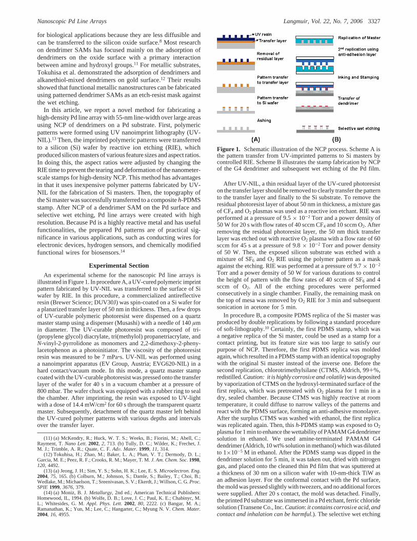
Figure 2 shows SEM images of the silicon masters with variousfeature distances fabricated by the procedure described in Figure1A. The line-widths, periods, and their standard deviations (SDs)of the prepared line patterns are listed in Table 1. All data inTable 1 were calculated by the SEM and AFM images. Morethan 50 lines were collected and measured for the average widthand SD. We fabricated several silicon masters with differentaspect ratios ranging from 1 to 4 by adjusting the SF6 RIE time.No specific difficulties occurred during the replication of PDMSstamps and NCP process for the feature scales larger than 100nm. However, when the line-width was sub-100-nm, the aspectratio of height to tip width should be optimized for a properreplication of PDMS stamps and a high resolution of NCP ofdendrimer. In the present case, when the aspect ratio of the patternwas below unity for a sub-100-nm line pattern, the dendrimerline array was printed poorly because of the roof collapse9 causedby low height contrast. Meanwhile, when the aspect ratio exceeded2, the PDMS mold was torn off. Consequently, the aspect ratioof the silicon master was kept at about 1.7 for the sub-100-nmscale pattern.
Interestingly, AFM image analysis of the silicon line patternshowed that the depth of the valley and the slanted angle of theside wall relative to the vertical depended on the feature scales.The narrower the etched valley width was, the lower patterndepth and the larger slant angle of side wall were developed.This was because the reactive gas could hardly reach the bottomof the valley, and the fluorinated silicon from the Si surface wasnot removed away readily from the narrower valley. Therefore,the side walls of narrow valleys in Figure 2C were slanted morethan those of wide ones in Figure 2A. However, when the line-width was as narrow as 43 nm in the case of Figure 2B, its side
wall was slanted despite the large width of the etched valleys.The slant for this narrow line-width was induced by thesimultaneous etching of the polymer mask and the Si wafer, asillustrated in Figure 2D. It is obvious that the side wall of thepolymeric mask on the silicon wafer is etched by the reactivegas dispersed after collision with the bottom layer, and the degreeof the side wall etching is pronounced for a narrower line-width.In our experimental condition, the width of the polymeric maskwas decreased as the RIE proceeded, which resulted in the slantedside wall of the Si line pattern. Obviously, the formation ofslanted walls can be suppressed by optimizing the RIE conditions(i.e., RIE gas composition, power, and exposure time), type ofthe resist, and aspect ratio of the mask. However, this is not ourinterest, and in the present case, the slanted profile facilitated thereplication of the PDMS mold being taken off from the Si master.
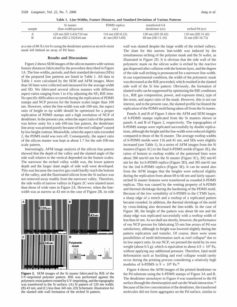
Panels A and B of Figure 3 show the AFM and SEM imagesof h-PDMS stamps replicated from the Si masters shown inpanels A and B of Figure 2, respectively. The topographies ofh-PDMS stamps were replicated successfully by double replica-tions, although the height and the line-width were reduced slightlycompared to those of the Si master. The average rooftop widthsof h-PDMS molds were 116 and 41 nm, and SDs were slightlyincreased (see Table 1). In a series of AFM images from the Simasters (Figure 3C) to the finalh-PDMS molds (Figure 3E), theratios of bottom to rooftop widths of the patterned lines wereabout 390 nm/43 nm for the Si master (Figure 3C), 392 nm/45nm for the 1sth-PDMS replica (Figure 3D), and 385 nm/41 nmfor the 2ndh-PDMS replica (Figure 3E). It can be noted alsofrom the AFM images that the heights were reduced slightlyduring the replication from about 69 to 66 nm and fairly square-etched Si master features were transferred as roundedh-PDMSreplicas. This was caused by the wetting property ofh-PDMSand thermal shrinkage during the hardening of the PDMS mold.Because of the low wettability ofh-PDMS to the CTMS layer,a sharp edge of a trench and a rooftop of a replicated patternbecame rounded. In addition, the thermal shrinkage of the moldby cross-linking also decreased the line-width. In the case ofFigure 3B, the height of the pattern was about 66 nm and thesharp edge was replicated successfully with a rooftop width ofless than 41 nm. As we shall see shortly, however, the performanceof our NCP process for fabricating 55-nm line arrays of Pd wassatisfactory, although its height was lowered slightly during thepattern replication and transfer. Of course, there were somepossibilities of mold deformation such as roof collapse9 due toits low aspect ratio. In our NCP, we pressed the mold by its ownweight (about 0.5 g), which is equivalent to about 4.9× 10² Pa,without applying any additional pressure. Therefore, fatal molddeformation such as buckling and roof collapse would rarelyoccur during the printing process considering a relatively highmodulus ofh-PDMS is 9× 10⁶ Pa.9c
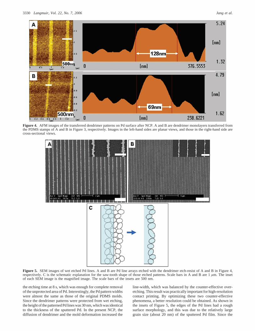
Figure 4 shows the AFM images of the printed dendrimer onthe Pd substrate using theh-PDMS stamps of Figure 3A and B.The dendrimer monolayer in Figure 4 was transferred to the Pdsurface through the chemisorption and van der Waals interaction.12
Because of the low concentration of the dendrimer, the transferredmolecules did not form aggregates on the Pd surface, similar to
Table 1. Line-Widths, Feature Distances, and Standard Deviations of Various Patterns
sampleSi master
(line-width/period)PDMS replica
(av)transferred G4dendrimer (av) etched Pd (av)
A 120 nm (SD 5.43)/710 nm 116 nm (SD 8.22) 128 nm (SD 20.42) 110 nm (SD 31.42)B 43 nm (SD 2.35)/616 nm 41 nm (SD 5.69) 69 nm (SD 11.19) 55 nm (SD 16.73)
Figure 2. SEM images of the Si master fabricated by RIE of theUV-imprinted polymer pattern. RIE was performed against thepolymeric resist pattern created by UV-imprinting, and the topographywas transferred to the Si surface. (A) Si pattern of 120 nm width;(B) 43 nm; and (C) less than 345 nm. (D) Schematic illustration forthe slanted side wall formation of the etched Si pattern.
3328 Langmuir, Vol. 22, No. 7, 2006 Jang et al.
those of Street et al. and Tsukruk et al. for silicon oxide substrate.15
However, the dendrimer line pattern transferred on the Pd surfacewas not as smooth as the PDMS stamp, but a little rough andirregular, as shown in Figure 4 because of irregular contact areaof the rounded roof-top, diffusion of the dendrimer, and surfaceroughness of the Pd substrate. The average thickness (ca. 1.7nm) of our dendrimer monolayer was slightly smaller than thereported values of 2.3 and 1.7-2.2 nm.15 (see AFM image inFigure S1 of the Supporting Information.) The lowered thicknesswas due to the stronger interaction of Pd with the amine groupsof the dendrimer than that of silicon oxide used in the previousstudies. The stronger the interaction, the more amine groupsreacted with Pd surface and dendrimer was deformed to theoblate shape. Therefore, the monolayer thickness on Pd wasthinner than that on the silicon oxide. As noted from Table 1,the widths and SDs of the printed dendrimer lines were increasedbecause of a weak diffusion of the dendrimer and roughness of
the Pd surface. In particular, the pattern widening became moresignificant as the line-width was reduced. This large wideningfor the narrower lines resulted mainly from mold deformation,as well as surface diffusion. Because the rooftops of the narrowerline pattern in case B of Table 1 was sharper than those in caseA for wider lines, a higher pressure was applied on the contactarea for case B, resulting in a larger widening.
Panels A and B of Figure 5 are the SEM images of the etchedPd patterns with two different widths of about 110 and 55 nm,respectively. In the case of the 55-nm Pd line, the whole areaover 5 mm× 5 mm was patterned homogeneously. As noted,the line-widths of Pd patterns were reduced from the corre-sponding widths of the printed dendrimer. This is because ofeither the intrinsic error in measuring the saw-tooth-like Pd line-width or the over-etching of the side wall of patterned Pd lines.Due to the etch-resist dendrimer, only the exposed area wasetched by the etchant. However, the side walls of the protectedarea were also etched at a low rate, and the width was decreasedsince the wet etching process proceeded isotropically. We fixed
(15) (a) Arrington, D.; Curry, M.; Street, S. C.Langmuir2002, 18, 7788. (b)Tsukruk, V. V.; Rinderspacher, F.; Bliznyuk V. N.Langmuir1997, 13, 2171.
Figure 3. SEM and AFM images of theh-PDMS stamps from the Si masters. A and B were replicated from the Si masters of A and Bin Figure 2, respectively. The insets are the corresponding SEM images. Scale bars are 1µm. C-E are the AFM images of the fabricatedpatterns. Images in the left-hand sides are planar views, and those in the right-hand side are cross-sectional views. (C) Si master transferredfrom UV-imprinted photoresist by scheme A of Figure 1. The ratio of bottom to rooftop widths of the Si master line is about 390 nm/43nm. (D) h-PDMS replica (1st replica) from the Si master. The ratio of top to bottom valley widths on the 1st replica is about 392 nm/45nm. (E)h-PDMS mold replicated from the 1st PDMS replica. The ratio of bottom to rooftop widths is about 385 nm/41 nm. Line heightswere reduced slightly during the replication from about 69 nm of the Si master to about 66 nm of the 2nd replica. The tip was rounded asshown in the topographic profile. The distances between the two red/yellow bars listed in the table below the cross-sectional images.
Nanoscopic Pd Line Arrays Langmuir, Vol. 22, No. 7, 20063329
the etching time at 8 s, which was enough for complete removalof the unprotected area of Pd. Interestingly, the Pd pattern widthswere almost the same as those of the original PDMS molds.Since the dendrimer patterns were protected from wet etching,the height of the patterned Pd lines was 30 nm, which was identicalto the thickness of the sputtered Pd. In the present NCP, thediffusion of dendrimer and the mold deformation increased the
line-width, which was balanced by the counter-effective over-etching. This result was practically important for high-resolutioncontact printing. By optimizing these two counter-effectivephenomena, a better resolution could be obtained. As shown inthe insets of Figure 5, the edges of the Pd lines had a roughsurface morphology, and this was due to the relatively largegrain size (about 20 nm) of the sputtered Pd film. Since the
Figure 4. AFM images of the transferred dendrimer patterns on Pd surface after NCP. A and B are dendrimer monolayers transferred fromthe PDMS stamps of A and B in Figure 3, respectively. Images in the left-hand sides are planar views, and those in the right-hand side arecross-sectional views.
Figure 5. SEM images of wet etched Pd lines. A and B are Pd line arrays etched with the dendrimer etch-resist of A and B in Figure 4,respectively. C is the schematic explanation for the saw-tooth shape of those etched patterns. Scale bars in A and B are 1µm. The insetof each SEM image is the magnified image. The scale bars of the insets are 500 nm.
3330 Langmuir, Vol. 22, No. 7, 2006 Jang et al.
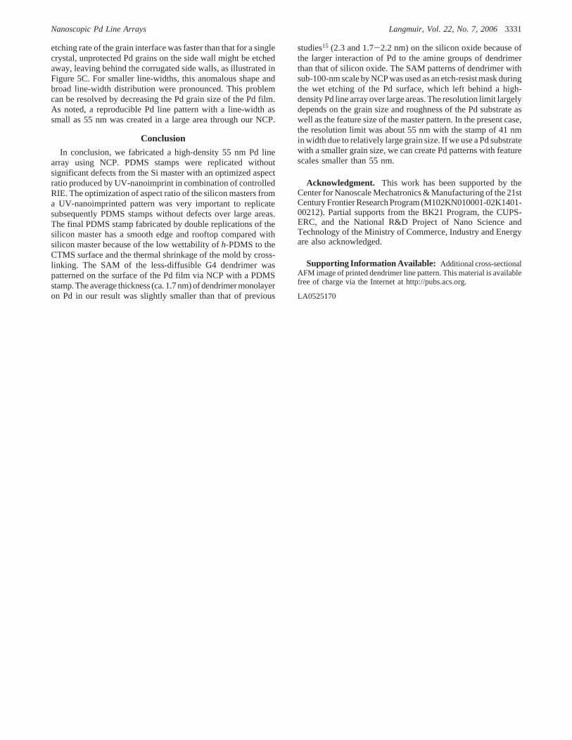
etching rate of the grain interface was faster than that for a singlecrystal, unprotected Pd grains on the side wall might be etchedaway, leaving behind the corrugated side walls, as illustrated inFigure 5C. For smaller line-widths, this anomalous shape andbroad line-width distribution were pronounced. This problemcan be resolved by decreasing the Pd grain size of the Pd film.As noted, a reproducible Pd line pattern with a line-width assmall as 55 nm was created in a large area through our NCP.
Conclusion
In conclusion, we fabricated a high-density 55 nm Pd linearray using NCP. PDMS stamps were replicated withoutsignificant defects from the Si master with an optimized aspectratio produced by UV-nanoimprint in combination of controlledRIE. The optimization of aspect ratio of the silicon masters froma UV-nanoimprinted pattern was very important to replicatesubsequently PDMS stamps without defects over large areas.The final PDMS stamp fabricated by double replications of thesilicon master has a smooth edge and rooftop compared withsilicon master because of the low wettability ofh-PDMS to theCTMS surface and the thermal shrinkage of the mold by cross-linking. The SAM of the less-diffusible G4 dendrimer waspatterned on the surface of the Pd film via NCP with a PDMSstamp. The average thickness (ca. 1.7 nm) of dendrimer monolayeron Pd in our result was slightly smaller than that of previous
studies15 (2.3 and 1.7-2.2 nm) on the silicon oxide because ofthe larger interaction of Pd to the amine groups of dendrimerthan that of silicon oxide. The SAM patterns of dendrimer withsub-100-nm scale by NCP was used as an etch-resist mask duringthe wet etching of the Pd surface, which left behind a high-density Pd line array over large areas. The resolution limit largelydepends on the grain size and roughness of the Pd substrate aswell as the feature size of the master pattern. In the present case,the resolution limit was about 55 nm with the stamp of 41 nmin width due to relatively large grain size. If we use a Pd substratewith a smaller grain size, we can create Pd patterns with featurescales smaller than 55 nm.
Acknowledgment. This work has been supported by theCenter for Nanoscale Mechatronics & Manufacturing of the 21stCentury Frontier Research Program (M102KN010001-02K1401-00212). Partial supports from the BK21 Program, the CUPS-ERC, and the National R&D Project of Nano Science andTechnology of the Ministry of Commerce, Industry and Energyare also acknowledged.
Supporting Information Available: Additional cross-sectionalAFM image of printed dendrimer line pattern. This material is availablefree of charge via the Internet at http://pubs.acs.org.
LA0525170
Nanoscopic Pd Line Arrays Langmuir, Vol. 22, No. 7, 20063331
Related Documents