This article appeared in a journal published by Elsevier. The attached copy is furnished to the author for internal non-commercial research and education use, including for instruction at the authors institution and sharing with colleagues. Other uses, including reproduction and distribution, or selling or licensing copies, or posting to personal, institutional or third party websites are prohibited. In most cases authors are permitted to post their version of the article (e.g. in Word or Tex form) to their personal website or institutional repository. Authors requiring further information regarding Elsevier’s archiving and manuscript policies are encouraged to visit: http://www.elsevier.com/copyright

Welcome message from author
This document is posted to help you gain knowledge. Please leave a comment to let me know what you think about it! Share it to your friends and learn new things together.
Transcript
This article appeared in a journal published by Elsevier. The attachedcopy is furnished to the author for internal non-commercial researchand education use, including for instruction at the authors institution
and sharing with colleagues.
Other uses, including reproduction and distribution, or selling orlicensing copies, or posting to personal, institutional or third party
websites are prohibited.
In most cases authors are permitted to post their version of thearticle (e.g. in Word or Tex form) to their personal website orinstitutional repository. Authors requiring further information
regarding Elsevier’s archiving and manuscript policies areencouraged to visit:
http://www.elsevier.com/copyright
Author's personal copy
Nanoscale patterning of functional perovskite-type complex oxides by pulsedlaser deposition through a nanostencil
Cristian-Victor Cojocaru 1, Riad Nechache, Catalin Harnagea, Alain Pignolet *, Federico Rosei *
INRS – Energie, Materiaux et Telecommunications, Universite du Quebec, 1650 Boulevard Lionel-Boulet, Varennes, QC J3X 1S2, Canada
1. Introduction
Following the trend of the semiconductor industry withrespect to the continuing miniaturization of integrated devices,functional oxide ceramic thin films are experiencing a similarevolution from microtechnology towards nanotechnology. In-creasing efforts are undertaken to nanostructure and pattern thinfilms of functional oxides and several recent reviews have debatedthe advantages and difficulties associated with either the top-down or the bottom-up approaches to pattern electroceramic thinfilms [1–5]. Although some of the alternative patterningtechniques to photolithography have already demonstrated thepotential to deliver structures with smallest features close to100 nm, their integration within a more general and complexfabrication scheme is very challenging. The requirement of perfectregistration is unavoidable for a process to be used in futuremicro- or nano-electronics.
As structure dimensions become progressively smaller, the newfunctional materials being envisioned often exhibit pronouncedsize effects which represent a significant deviation of theproperties of low-dimensional structures with respect to theirbulk properties [6,7]. The ‘‘size effect’’ in ferroelectrics, induced bya reduction in geometrical dimensions, has been shown to result,among other phenomena, in a reduced remnant polarization anddielectric permittivity, in changes in the domain structure, a
decrease of the phase transition temperature and an increase of thecoercive field [8]. Fundamental studies of patterned functionaloxide ceramics are further required for these new materials,especially in the nanoscale regime. These studies are crucial toestablish experimentally the useful critical size for each material,i.e. the smallest size at which it would still provide the desiredfunctionality [9–15]. In the particular case of ferroelectricmaterials, theoretical predictions suggest that, due to an increasingrole of the depolarization field and the weakening of long rangecooperative interactions, which are the driving force for ferroelec-tricity, the latter is supposed to disappear below a critical size.These calculations suggest a material-dependent critical thicknessand correlation volume (e.g. 2.4 nm for a BaTiO3 thin film betweentwo metallic SrRuO3 electrodes) [16]. Other theoretical studies onsize effects estimated the minimum volume at which thepolarization and the ferroelectric properties should vanish (criticalvolume) to be about 1000 nm3 [17]. Experimental studiesdemonstrated that ferroelectricity exists in ultrathin (4 nm)Pb(Zr,Ti)O3 (PZT) epitaxial films [18] and ferroelectricity wasobserved in BaTiO3 (BTO) films about 5 nm thick [19]. Such sizeeffects in general are poorly understood.
The top-down methods that are currently used in nanotech-nology provide high-precision positioning and size control yet areoften limited in resolution or are not suitable for complex oxidematerials. For example, a conventional patterning process, basedon usual resist lithography followed by etching of the oxide film isfraught with severe problems, when applied to ferroelectric thinfilms: contamination and side-wall redeposition can alter thepolarization switching (even for features as large as micrometers)and constitutes challenging issues to be overcome in thepatterning of complex oxides in general and of ferroelectric thin
Applied Surface Science 256 (2010) 4777–4783
A R T I C L E I N F O
Article history:
Available online 4 February 2010
Keywords:
Parallel patterning
Nanostencil lithography
Pulsed laser deposition (PLD)
Perovskite complex oxides
Ferroelectric nanostructures
Barium titanate
A B S T R A C T
We present studies on parallel nanoscale patterning of piezoelectrics/ferroelectrics via deposition
through a nanostencil. Unlike other processes reported for oxide nanostructuring, we selectively deposit
the material, directly, by interposing a nanosieve between the substrate and the deposition source. We
show that this selective deposition can be realized even with materials as complex as perovskite oxides,
both at room temperature and at high temperature. We elaborate on and analyze the performance of the
nanostenciling approach for the growth of barium titanate BaTiO3 on strontium titanate SrTiO3(1 0 0).
The patterned structures of ferroelectric materials are characterized by X-ray diffraction and imaged
locally by scanning probe microscopy in piezoresponse mode to individually probe their functionality.
� 2010 Elsevier B.V. All rights reserved.
* Corresponding authors.
E-mail addresses: [email protected] (A. Pignolet), [email protected]
(F. Rosei).1 Present address: NRC-Industrial Materials Institute, Boucherville, QC, Canada.
Contents lists available at ScienceDirect
Applied Surface Science
journa l homepage: www.e lsev ier .com/ locate /apsusc
0169-4332/$ – see front matter � 2010 Elsevier B.V. All rights reserved.
doi:10.1016/j.apsusc.2010.01.103
Author's personal copy
films in particular. Alternatively, bottom-up strategies, either byphysical or chemical self-patterning of complex oxides [20,21]hold the promise of realizing much smaller features than thoseachievable with top-down techniques. Self-assembly governed bygrowth mechanisms similar to those found for Ge islanding onSi(0 0 1) surfaces [22], overcome the low throughput and proces-sing damage of conventional patterning methods [12]. Neverthe-less, they suffer from poor registration and to achieve a certainorganization requires prior substrate patterning, which in turninvolves an additional top-down processing step [23]. Thoughappealing for scientific purposes, bottom-up approaches arepresently still ineffective, somewhat unreliable and not yet ripeto be implemented as new technologies.
We present here studies on parallel nanostructuring andpatterning of ferroic oxides, mainly piezoelectrics/ferroelectrics,via pulsed laser deposition (PLD) through a nanostencil. Theoriginal aim was to assess whether nanostenciling can become ageneral-purpose nanoscale patterning technique that offers bothhigh resolution and unique flexibility for any combination ofdeposited material/substrate. Unlike most of the other techniquesreported for oxide nanostructuring, we do not process or modifythe substrate, but selectively deposit the material, directly, byinterposing the nanosieve between the substrate and the deposi-tion source. Simultaneously, there is an inherent control of thelocations where the nucleation starts and where the structures’growth will further take place, if the stencil is accuratelypositioned with respect to the substrate. A direct copy of theapertures opened in the stencil is realized on the substrate by‘‘forcing’’ the material to pass through the former providing thus atechnique for parallel fabrication of ordered arrays of islands. Asimilar approach has been investigated independently by othergroups [24–26]. In particular, we compare patterns of BaTiO3 (acompound less sensitive to variations in by depositing parameters)obtained by both room temperature deposition (and crystallizedby subsequent annealing) and by depositing at high temperature.The patterned structures of ferroelectric materials are character-ized by X-ray diffraction (XRD) and probed locally by scanningforce microscopy in piezoresponse mode for ferroelectricity.
2. Experimental
PLD patterning experiments were conducted using laserinterference lithography (LIL)-based stencil masks, with built-in500 nm thick Si3N4 nanosieves with circular apertures. Thesestencils have hexagonal arrays of pores (350 nm in diameter) witha periodicity of either 1.6 mm or 700 nm and are patterned on 12–14 free-standing, low stress (LS-SiN) membranes (2 mm in lengthand 100 mm in width each, 100 mm apart). The Si3N4 membranesare prepared on single crystal Si(1 0 0) wafers 380 mm thick andthe stencil’s dimension is 5 mm � 5 mm with an active area of�2 mm � 2.7 mm. The stencils were mechanically clamped andtemporarily fixed onto Nb-doped (1 0 0)-oriented SrTiO3 sub-strates. The assembly substrate-stencil was mounted in thevacuum chamber of a PLD system, in front of a dense BaTiO3
stoichiometric ceramic rotating target. A KrF Lumonics PM-800excimer laser (radiation with l = 248 nm, pulse duration = 15.4 ns)was employed for ablation with a 458 incidence angle on thetarget and a laser fluence of 2 J/cm2. A set of depositions werecarried out at room temperature (RT), in vacuum at 1 � 10�5 mbar(7.5 � 10�3 mTorr), with a laser repetition rate ranging from 5 to10 Hz and a target–substrate distance of 6.5–7 cm. We furtherpursued the nanostenciling of BaTiO3 directly at high temperature,in low O2 background gas conditions according to the parametersprovided in Table 1. This was possible only thanks to the highthermal resistance and stability of the Si3N4 membranes attemperatures up to 800 8C.
All the samples were prepared on SrTiO3 single crystallinesubstrates (0 0 1)-oriented, using the same number of laserablation pulses (N = 5000) and stencils with the same aperturediameter (350 nm). Two samples were fabricated with stencilshaving periodic apertures spaced with 1.6 mm pitch. Afterdeposition the samples were cooled down to room temperature,naturally, in a 150 mTorr O2 background pressure. Once thedeposition was completed the stencils were unclamped and simply‘‘lifted off’’ (separated) from the substrate. The properties of acontinuous epitaxial film (�100 nm thick) deposited in high O2
atmosphere were also investigated.X-ray diffraction in grazing incidence (GIXRD) and Bragg–
Brentano (u–2u) configuration was used to investigate thecrystalline phases present in the patterned structures and theirquality. The lattice parameters of the epitaxially patterned sampleswere studied more in detail by X-ray reciprocal space mapping(RSM), a technique typically used in epitaxial films to determinethe strain state in thin films.
Local ferroelectric testing was performed using PiezoresponseForce Microscopy (PFM) as described earlier [27]. We applied asmall AC voltage (typically 0.5 V at 29 kHz) between theconductive AFM tip and the sample bottom electrode. Hysteresisloops were acquired by positioning the AFM tip over the center ofan individual nanostructure, then the local piezoresponse signalwas recorded while a superimposed DC bias voltage was sweptbetween �10 V and +10 V. The induced local mechanicaldisplacement was detected, using long integration times for thelock-in amplifier connected to the AFM. The out-of-planepiezoelectric coefficient d33 was calibrated according to theprocedure developed by Harnagea and Pignolet [28].
3. Results and discussion
3.1. Stencil lifetime
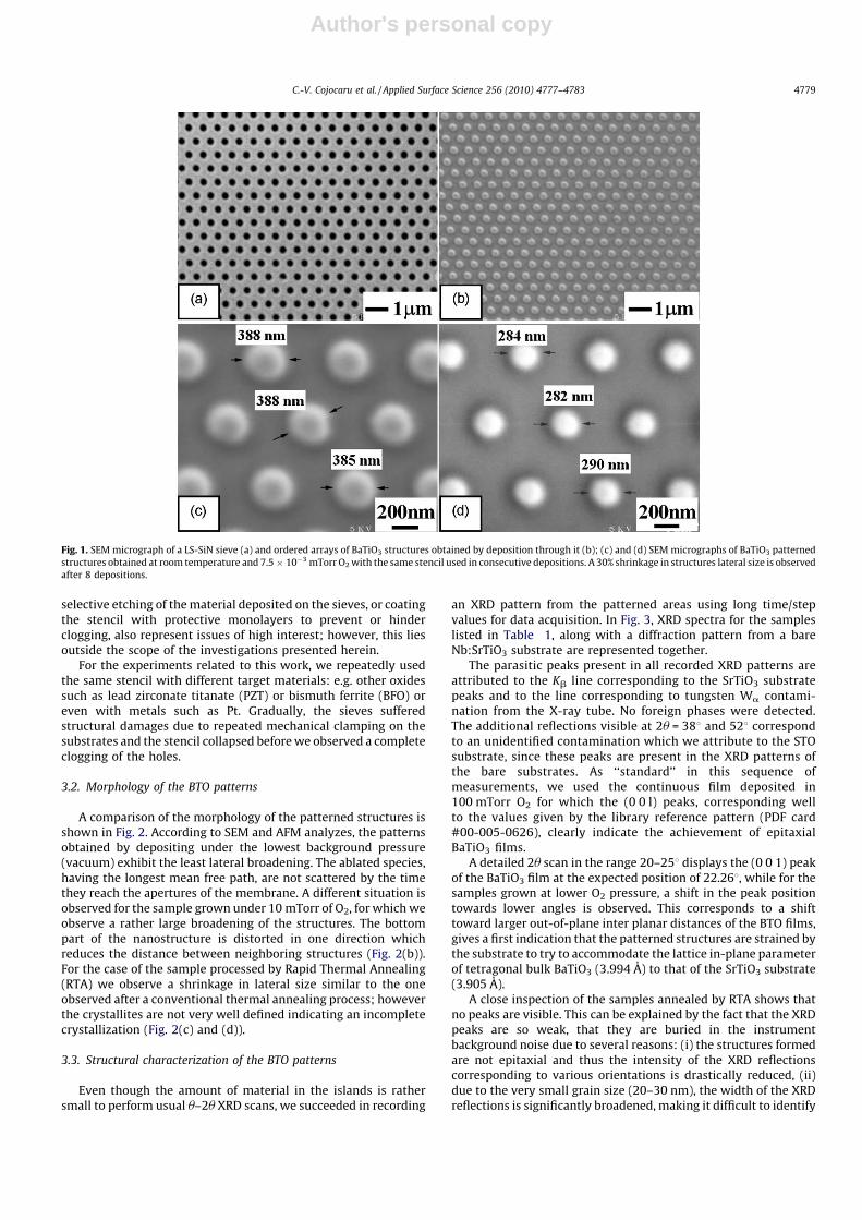
Rapid and parallel fabrication of ordered BTO nanostructureswas achieved at RT in a single deposition step, over the whole sieveareas. Fig. 1(a) displays an SEM micrograph detail from a LS-Si3N4
nanosieve with pores of 350 nm in diameter and a 700 nm pitchused during the depositions and Fig. 1(b) shows the well-ordered,dome-shaped, as-deposited structures, obtained via stencilingthrough the latter.
The SEM micrograph in Fig. 1(c) reveals structures with baseenlarged to 385–390 nm and thus suggesting an overall basebroadening of�35–40 nm, i.e.�10% larger than the nominal valueof the apertures. We found that, for the sieves with 350 nmdiameter circular holes, the transfer efficiency (defined as the ratiobetween the height of the structures and the thickness of a filmdeposited in the same conditions) is above 80%.
Subsequent depositions using the same stencils revealed thatfor a total, nominal thickness of the deposited BTO equivalent to3.5 times the aperture diameter, the lateral size of the replicatedstructures shrank by 30% (Fig. 1(d)).
The choice of the physical vapor deposition technique used incombination with nanostenciling plays an important role and thecontrol of the interaction of the material to be deposited, with themembrane apertures, remains a matter of further examination.Identifying efficient cleaning recipes for the stencils, such as
Table 1Deposition conditions for the patterns analyzed in this work.
ID Temperature Pressure
[O2] (mTorr)
Post-deposition
annealing
BTO pattern I 620 8C 7.5�10�3 N/A
BTO pattern II 620 8C 10 N/A
BTO pattern III RT 7.5�10�3 RTA–700 8C
C.-V. Cojocaru et al. / Applied Surface Science 256 (2010) 4777–47834778
Author's personal copy
selective etching of the material deposited on the sieves, or coatingthe stencil with protective monolayers to prevent or hinderclogging, also represent issues of high interest; however, this liesoutside the scope of the investigations presented herein.
For the experiments related to this work, we repeatedly usedthe same stencil with different target materials: e.g. other oxidessuch as lead zirconate titanate (PZT) or bismuth ferrite (BFO) oreven with metals such as Pt. Gradually, the sieves sufferedstructural damages due to repeated mechanical clamping on thesubstrates and the stencil collapsed before we observed a completeclogging of the holes.
3.2. Morphology of the BTO patterns
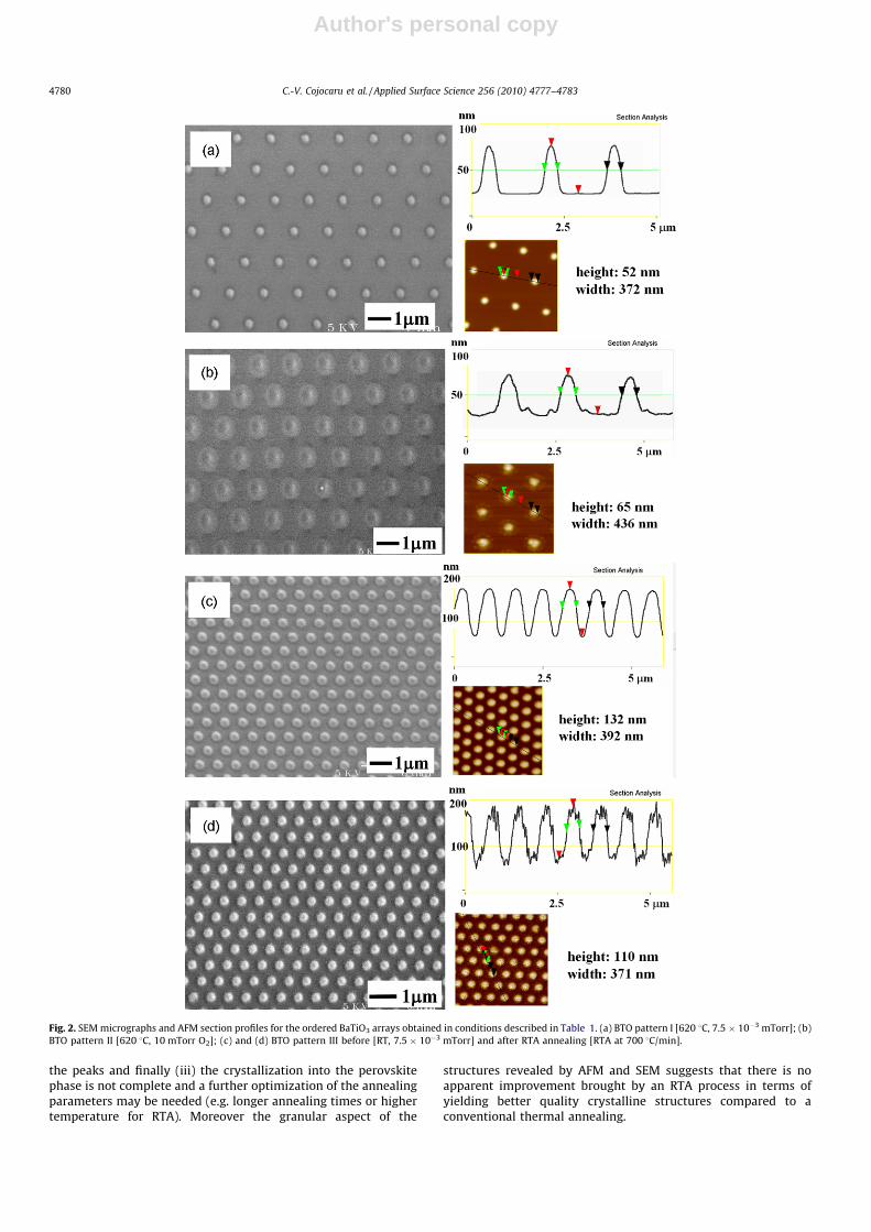
A comparison of the morphology of the patterned structures isshown in Fig. 2. According to SEM and AFM analyzes, the patternsobtained by depositing under the lowest background pressure(vacuum) exhibit the least lateral broadening. The ablated species,having the longest mean free path, are not scattered by the timethey reach the apertures of the membrane. A different situation isobserved for the sample grown under 10 mTorr of O2, for which weobserve a rather large broadening of the structures. The bottompart of the nanostructure is distorted in one direction whichreduces the distance between neighboring structures (Fig. 2(b)).For the case of the sample processed by Rapid Thermal Annealing(RTA) we observe a shrinkage in lateral size similar to the oneobserved after a conventional thermal annealing process; howeverthe crystallites are not very well defined indicating an incompletecrystallization (Fig. 2(c) and (d)).
3.3. Structural characterization of the BTO patterns
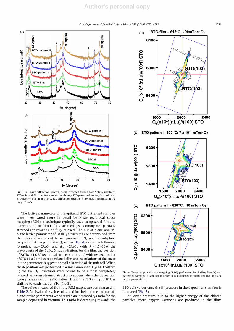
Even though the amount of material in the islands is rathersmall to perform usual u–2u XRD scans, we succeeded in recording
an XRD pattern from the patterned areas using long time/stepvalues for data acquisition. In Fig. 3, XRD spectra for the sampleslisted in Table 1, along with a diffraction pattern from a bareNb:SrTiO3 substrate are represented together.
The parasitic peaks present in all recorded XRD patterns areattributed to the Kb line corresponding to the SrTiO3 substratepeaks and to the line corresponding to tungsten Wa contami-nation from the X-ray tube. No foreign phases were detected.The additional reflections visible at 2u = 388 and 528 correspondto an unidentified contamination which we attribute to the STOsubstrate, since these peaks are present in the XRD patterns ofthe bare substrates. As ‘‘standard’’ in this sequence ofmeasurements, we used the continuous film deposited in100 mTorr O2 for which the (0 0 l) peaks, corresponding wellto the values given by the library reference pattern (PDF card#00-005-0626), clearly indicate the achievement of epitaxialBaTiO3 films.
A detailed 2u scan in the range 20–258 displays the (0 0 1) peakof the BaTiO3 film at the expected position of 22.268, while for thesamples grown at lower O2 pressure, a shift in the peak positiontowards lower angles is observed. This corresponds to a shifttoward larger out-of-plane inter planar distances of the BTO films,gives a first indication that the patterned structures are strained bythe substrate to try to accommodate the lattice in-plane parameterof tetragonal bulk BaTiO3 (3.994 A) to that of the SrTiO3 substrate(3.905 A).
A close inspection of the samples annealed by RTA shows thatno peaks are visible. This can be explained by the fact that the XRDpeaks are so weak, that they are buried in the instrumentbackground noise due to several reasons: (i) the structures formedare not epitaxial and thus the intensity of the XRD reflectionscorresponding to various orientations is drastically reduced, (ii)due to the very small grain size (20–30 nm), the width of the XRDreflections is significantly broadened, making it difficult to identify
Fig. 1. SEM micrograph of a LS-SiN sieve (a) and ordered arrays of BaTiO3 structures obtained by deposition through it (b); (c) and (d) SEM micrographs of BaTiO3 patterned
structures obtained at room temperature and 7.5 � 10�3 mTorr O2 with the same stencil used in consecutive depositions. A 30% shrinkage in structures lateral size is observed
after 8 depositions.
C.-V. Cojocaru et al. / Applied Surface Science 256 (2010) 4777–4783 4779
Author's personal copy
the peaks and finally (iii) the crystallization into the perovskitephase is not complete and a further optimization of the annealingparameters may be needed (e.g. longer annealing times or highertemperature for RTA). Moreover the granular aspect of the
structures revealed by AFM and SEM suggests that there is noapparent improvement brought by an RTA process in terms ofyielding better quality crystalline structures compared to aconventional thermal annealing.
Fig. 2. SEM micrographs and AFM section profiles for the ordered BaTiO3 arrays obtained in conditions described in Table 1. (a) BTO pattern I [620 8C, 7.5 � 10�3 mTorr]; (b)
BTO pattern II [620 8C, 10 mTorr O2]; (c) and (d) BTO pattern III before [RT, 7.5 � 10�3 mTorr] and after RTA annealing [RTA at 700 8C/min].
C.-V. Cojocaru et al. / Applied Surface Science 256 (2010) 4777–47834780
Author's personal copy
The lattice parameters of the epitaxial BTO patterned sampleswere investigated more in detail by X-ray reciprocal spacemapping (RSM), a technique typically used in epitaxial films todetermine if the film is fully strained (pseudomorphic), partiallystrained (or relaxed), or fully relaxed. The out-of-plane and in-plane lattice parameter of BaTiO3 structures are determined fromthe in-plane reciprocal lattice parameter Qx and out-of-planereciprocal lattice parameter Qy values (Fig. 4) using the followingformulas: din = 2l/Qx and dout = 2l/Qy with l = 1.5406 A thewavelength of the Cu Ka X-ray radiation. For the film, the positionof BaTiO3 (1 0 3) reciprocal lattice point (r.l.p.) with respect to thatof STO (1 0 3) indicates a relaxed film and calculations of the exactlattice parameters suggests a small distortion of the unit cell. Whenthe deposition was performed in a small amount of O2 (BTO patternII) the BaTiO3 structures were found to be almost completelyrelaxed, whereas strained structures appear when the depositiontakes place in vacuum (BTO pattern I) and the (1 0 3) r.l.p. of BTO isshifting towards that of STO (1 0 3).
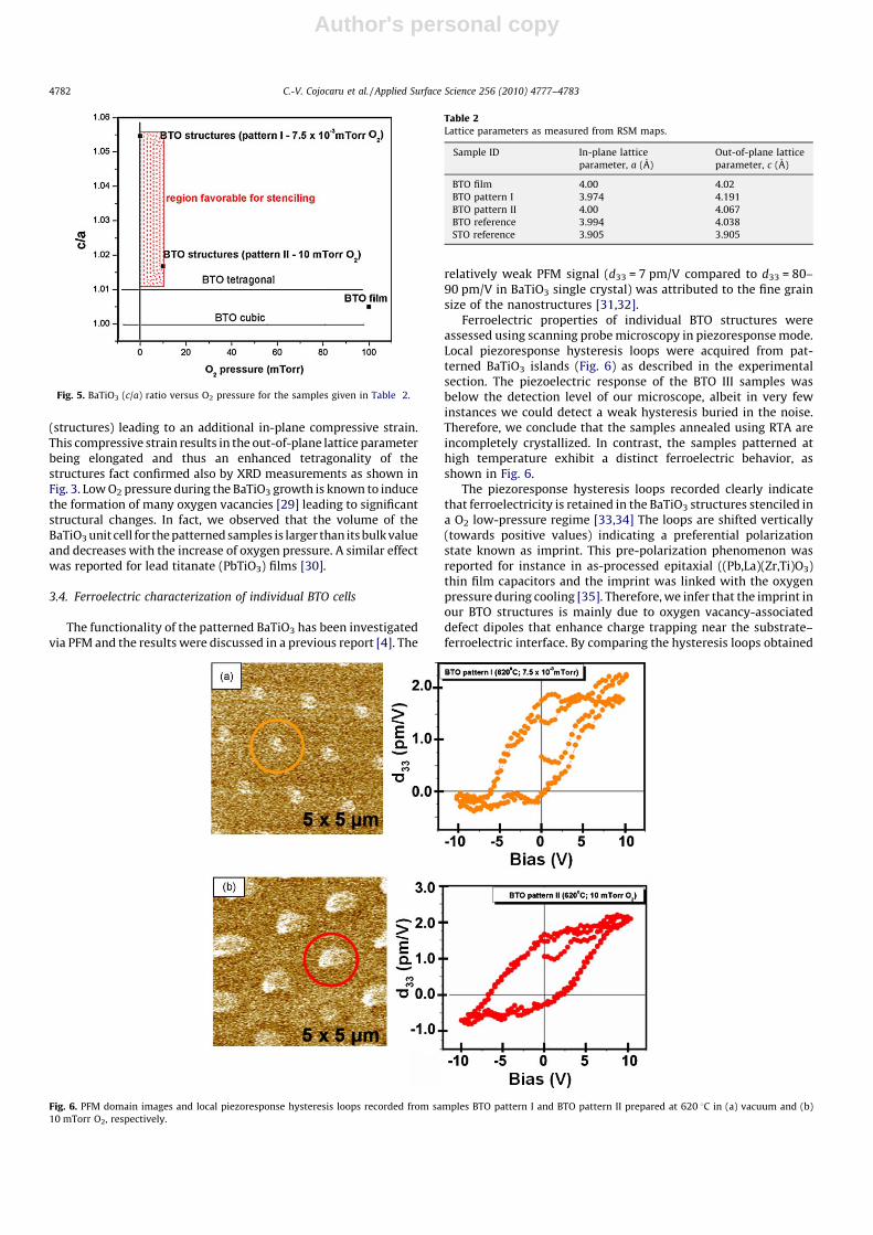
The values measured from the RSM graphs are summarized inTable 2. Analyzing the values obtained for the in-plane and out-of-plane lattice parameters we observed an increased c/a ratio for thesample deposited in vacuum. This ratio is decreasing towards the
BTO bulk values once the O2 pressure in the deposition chamber isincreased (Fig. 5).
At lower pressure, due to the higher energy of the ablatedparticles, more oxygen vacancies are produced in the films
Fig. 3. (a) X-ray diffraction spectra (u–2u) recorded from a bare SrTiO3 substrate,
BTO epitaxial film and from an area with only BTO patterned arrays, denominated
BTO pattern I, II, III and (b) X-ray diffraction spectra (u–2u) detail recorded in the
range 20–258.
Fig. 4. X-ray reciprocal space mapping (RSM) performed for: BaTiO3 film (a) and
patterned samples (b) and (c), in order to calculate the in-plane and out-of-plane
lattice parameters.
C.-V. Cojocaru et al. / Applied Surface Science 256 (2010) 4777–4783 4781
Author's personal copy
(structures) leading to an additional in-plane compressive strain.This compressive strain results in the out-of-plane lattice parameterbeing elongated and thus an enhanced tetragonality of thestructures fact confirmed also by XRD measurements as shown inFig. 3. Low O2 pressure during the BaTiO3 growth is known to inducethe formation of many oxygen vacancies [29] leading to significantstructural changes. In fact, we observed that the volume of theBaTiO3 unit cell for the patterned samples is larger than its bulk valueand decreases with the increase of oxygen pressure. A similar effectwas reported for lead titanate (PbTiO3) films [30].
3.4. Ferroelectric characterization of individual BTO cells
The functionality of the patterned BaTiO3 has been investigatedvia PFM and the results were discussed in a previous report [4]. The
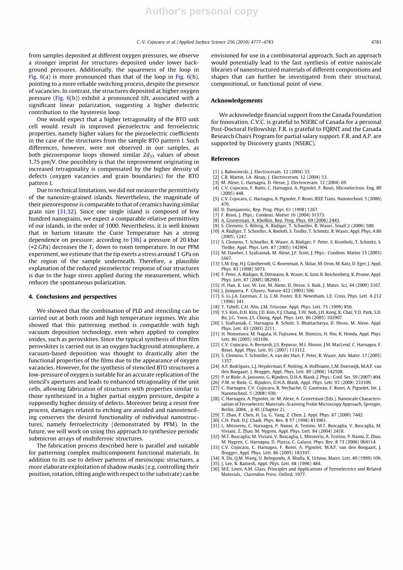
relatively weak PFM signal (d33 = 7 pm/V compared to d33 = 80–90 pm/V in BaTiO3 single crystal) was attributed to the fine grainsize of the nanostructures [31,32].
Ferroelectric properties of individual BTO structures wereassessed using scanning probe microscopy in piezoresponse mode.Local piezoresponse hysteresis loops were acquired from pat-terned BaTiO3 islands (Fig. 6) as described in the experimentalsection. The piezoelectric response of the BTO III samples wasbelow the detection level of our microscope, albeit in very fewinstances we could detect a weak hysteresis buried in the noise.Therefore, we conclude that the samples annealed using RTA areincompletely crystallized. In contrast, the samples patterned athigh temperature exhibit a distinct ferroelectric behavior, asshown in Fig. 6.
The piezoresponse hysteresis loops recorded clearly indicatethat ferroelectricity is retained in the BaTiO3 structures stenciled ina O2 low-pressure regime [33,34] The loops are shifted vertically(towards positive values) indicating a preferential polarizationstate known as imprint. This pre-polarization phenomenon wasreported for instance in as-processed epitaxial ((Pb,La)(Zr,Ti)O3)thin film capacitors and the imprint was linked with the oxygenpressure during cooling [35]. Therefore, we infer that the imprint inour BTO structures is mainly due to oxygen vacancy-associateddefect dipoles that enhance charge trapping near the substrate–ferroelectric interface. By comparing the hysteresis loops obtained
Table 2Lattice parameters as measured from RSM maps.
Sample ID In-plane lattice
parameter, a (A)
Out-of-plane lattice
parameter, c (A)
BTO film 4.00 4.02
BTO pattern I 3.974 4.191
BTO pattern II 4.00 4.067
BTO reference 3.994 4.038
STO reference 3.905 3.905
Fig. 5. BaTiO3 (c/a) ratio versus O2 pressure for the samples given in Table 2.
Fig. 6. PFM domain images and local piezoresponse hysteresis loops recorded from samples BTO pattern I and BTO pattern II prepared at 620 8C in (a) vacuum and (b)
10 mTorr O2, respectively.
C.-V. Cojocaru et al. / Applied Surface Science 256 (2010) 4777–47834782
Author's personal copy
from samples deposited at different oxygen pressures, we observea stronger imprint for structures deposited under lower back-ground pressures. Additionally, the squareness of the loop inFig. 6(a) is more pronounced than that of the loop in Fig. 6(b),pointing to a more reliable switching process, despite the presenceof vacancies. In contrast, the structures deposited at higher oxygenpressure (Fig. 6(b)) exhibit a pronounced tilt, associated with asignificant linear polarization, suggesting a higher dielectriccontribution to the hysteresis loop.
One would expect that a higher tetragonality of the BTO unitcell would result in improved piezoelectric and ferroelectricproperties, namely higher values for the piezoelectric coefficientsin the case of the structures from the sample BTO pattern I. Suchdifferences, however, were not observed in our samples, asboth piezoresponse loops showed similar 2d33 values of about1.75 pm/V. One possibility is that the improvement originating inincreased tetragonality is compensated by the higher density ofdefects (oxygen vacancies and grain boundaries) for the BTOpattern I.
Due to technical limitations, we did not measure the permittivityof the nanosize-grained islands. Nevertheless, the magnitude oftheir piezoresponse is comparable to that of ceramics having similargrain size [31,32]. Since one single island is composed of fewhundred nanograins, we expect a comparable relative permittivityof our islands, in the order of 1000. Nevertheless, it is well knownthat in barium titanate the Curie Temperature has a strongdependence on pressure; according to [36] a pressure of 20 kbar(=2 GPa) decreases the Tc down to room temperature. In our PFMexperiment, we estimate that the tip exerts a stress around 1 GPa onthe region of the sample underneath. Therefore, a plausibleexplanation of the reduced piezoelectric response of our structuresis due to the huge stress applied during the measurement, whichreduces the spontaneous polarization.
4. Conclusions and perspectives
We showed that the combination of PLD and stenciling can becarried out at both room and high temperature regimes. We alsoshowed that this patterning method is compatible with highvacuum deposition technology, even when applied to complexoxides, such as perovskites. Since the typical synthesis of thin filmperovskites is carried out in an oxygen background atmosphere, avacuum-based deposition was thought to drastically alter thefunctional properties of the films due to the appearance of oxygenvacancies. However, for the synthesis of stenciled BTO structures alow-pressure of oxygen is suitable for an accurate replication of thestencil’s apertures and leads to enhanced tetragonality of the unitcells, allowing fabrication of structures with properties similar tothose synthesized in a higher partial oxygen pressure, despite asupposedly higher density of defects. Moreover being a resist freeprocess, damages related to etching are avoided and nanostencil-ing conserves the desired functionality of individual nanostruc-tures, namely ferroelectricity (demonstrated by PFM). In thefuture, we will work on using this approach to synthesize periodicsubmicron arrays of multiferroic structures.
The fabrication process described here is parallel and suitablefor patterning complex multicomponent functional materials. Inaddition to its use to deliver patterns of mesoscopic structures, amore elaborate exploitation of shadow masks (e.g. controlling theirposition, rotation, tilting angle with respect to the substrate) can be
envisioned for use in a combinatorial approach. Such an approachwould potentially lead to the fast synthesis of entire nanoscalelibraries of nanostructured materials of different compositions andshapes that can further be investigated from their structural,compositional, or functional point of view.
Acknowledgements
We acknowledge financial support from the Canada Foundationfor Innovation. C.V.C. is grateful to NSERC of Canada for a personalPost-Doctoral Fellowship. F.R. is grateful to FQRNT and the CanadaResearch Chairs Program for partial salary support. F.R. and A.P. aresupported by Discovery grants (NSERC).
References
[1] J. Baborowski, J. Electroceram. 12 (2004) 33.[2] C.R. Martin, I.A. Aksay, J. Electroceram. 12 (2004) 53.[3] M. Alexe, C. Harnagea, D. Hesse, J. Electroceram. 12 (2004) 69.[4] C.V. Cojocaru, F. Ratto, C. Harnagea, A. Pignolet, F. Rosei, Microelectron. Eng. 80
(2005) 448.[5] C.V. Cojocaru, C. Harnagea, A. Pignolet, F. Rosei, IEEE Trans. Nanotechnol. 5 (2006)
470.[6] D. Damjanovic, Rep. Prog. Phys. 61 (1998) 1267.[7] F. Rosei, J. Phys.: Condens. Matter 16 (2004) S1373.[8] A. Gruverman, A. Kholkin, Rep. Prog. Phys. 69 (2006) 2443.[9] S. Clemens, S. Rohrig, A. Rudiger, T. Schneller, R. Waser, Small 2 (2006) 500.
[10] A. Rudiger, T. Schneller, A. Roelofs, S. Tiedke, T. Schmitz, R. Waser, Appl. Phys. A 80(2005) 1247.
[11] S. Clemens, T. Schneller, R. Waser, A. Rudiger, F. Peter, S. Kronholz, T. Schmitz, S.Tiedke, Appl. Phys. Lett. 87 (2005) 142904.
[12] M. Dawber, I. Szafraniak, M. Alexe, J.F. Scott, J. Phys.: Condens. Matter 15 (2003)L667.
[13] L.M. Eng, H.J. Guntherodt, G. Rosenman, A. Skliar, M. Oron, M. Katz, D. Eger, J. Appl.Phys. 83 (1998) 5973.
[14] F. Peter, A. Rudiger, R. Dittmann, R. Waser, K. Szot, B. Reichenberg, K. Prume, Appl.Phys. Lett. 87 (2005) 082901.
[15] H. Han, K. Lee, W. Lee, M. Alexe, D. Hesse, S. Baik, J. Mater. Sci. 44 (2009) 5167.[16] J. Junquera, P. Ghosez, Nature 422 (2003) 506.[17] S. Li, J.A. Eastman, Z. Li, C.M. Foster, R.E. Newnham, L.E. Cross, Phys. Lett. A 212
(1996) 341.[18] T. Tybell, C.H. Ahn, J.M. Triscone, Appl. Phys. Lett. 75 (1999) 856.[19] Y.S. Kim, D.H. Kim, J.D. Kim, Y.J. Chang, T.W. Noh, J.H. Kong, K. Char, Y.D. Park, S.D.
Bu, J.G. Yoon, J.S. Chung, Appl. Phys. Lett. 86 (2005) 102907.[20] I. Szafraniak, C. Harnagea, R. Scholz, S. Bhattacharya, D. Hesse, M. Alexe, Appl.
Phys. Lett. 83 (2003) 2211.[21] H. Nonomura, M. Nagata, H. Fujisawa, M. Shimizu, H. Niu, K. Honda, Appl. Phys.
Lett. 86 (2005) 163106.[22] C.V. Cojocaru, A. Bernardi, J.S. Reparaz, M.I. Alonso, J.M. MacLeod, C. Harnagea, F.
Rosei, Appl. Phys. Lett. 91 (2007) 113112.[23] S. Clemens, T. Schneller, A. van der Hart, F. Peter, R. Waser, Adv. Mater. 17 (2005)
1357.[24] A.F. Rodrıguez, L.J. Heyderman, F. Nolting, A. Hoffmann, L.M. Doeswijk, M.A.F. van
den Boogaart, J. Brugger, Appl. Phys. Lett. 89 (2006) 142508.[25] P. te Riele, A. Janssens, G. Rijnders, D.H.A. Blank, J. Phys.: Conf. Ser. 59 (2007) 404.[26] P.M. te Riele, G. Rijnders, D.H.A. Blank, Appl. Phys. Lett. 93 (2008) 233109.[27] C. Harnagea, C.V. Cojocaru, R. Nechache, O. Gautreau, F. Rosei, A. Pignolet, Int. J.
Nanotechnol. 5 (2008) 930.[28] C. Harnagea, A. Pignolet, in: M. Alexe, A. Gruverman (Eds.), Nanoscale Characteri-
sation of Ferroelectric Materials–Scanning Probe Microscopy Approach, Springer,Berlin, 2004, , p 45 (Chapter 2).
[29] T. Zhao, F. Chen, H. Lu, G. Yang, Z. Chen, J. Appl. Phys. 87 (2000) 7442.[30] C.H. Park, D.J. Chadi, Phys. Rev. B 57 (1998) R13961.[31] L. Mitoseriu, C. Harnagea, P. Nanni, A. Testino, M.T. Buscaglia, V. Buscaglia, M.
Viviani, Z. Zhao, M. Nygren, Appl. Phys. Lett. 84 (2004) 2418.[32] M.T. Buscaglia, M. Viviani, V. Buscaglia, L. Mitoseriu, A. Testino, P. Nanni, Z. Zhao,
M. Nygren, C. Harnagea, D. Piazza, C. Galassi, Phys. Rev. B 73 (2006) 064114.[33] C.V. Cojocaru, C. Harnagea, F. Rosei, A. Pignolet, M.A.F. van den Boogaart, J.
Brugger, Appl. Phys. Lett. 86 (2005) 183107.[34] X. Du, Q.M. Wang, U. Belegundu, A. Bhalla, K. Uchino, Mater. Lett. 40 (1999) 109.[35] J. Lee, R. Ramesh, Appl. Phys. Lett. 68 (1996) 484.[36] M.E. Lines, A.M. Glass, Principles and Applications of Ferroelectrics and Related
Materials, Clarendon Press, Oxford, 1977.
C.-V. Cojocaru et al. / Applied Surface Science 256 (2010) 4777–4783 4783
Related Documents


![PEROVSKITE-TYPE OXIDES - THE NEW APPROACH TO … · PEROVSKITE-TYPE OXIDES - THE NEW APPROACH TO HIGH-T c ... it was the result of the short episode of my activities in ... [1.7]](https://static.cupdf.com/doc/110x72/5b0a90ae7f8b9abe5d8e6247/perovskite-type-oxides-the-new-approach-to-oxides-the-new-approach-to-high-t.jpg)