Washington University in St. Louis Washington University Open Scholarship Engineering and Applied Science eses & Dissertations McKelvey School of Engineering Winter 12-15-2018 Nanopower Analog Frontends for Cyber-Physical Systems Kenji Aono Washington University in St. Louis Follow this and additional works at: hps://openscholarship.wustl.edu/eng_etds Part of the Computer Engineering Commons , Computer Sciences Commons , and the Electrical and Electronics Commons is Dissertation is brought to you for free and open access by the McKelvey School of Engineering at Washington University Open Scholarship. It has been accepted for inclusion in Engineering and Applied Science eses & Dissertations by an authorized administrator of Washington University Open Scholarship. For more information, please contact [email protected]. Recommended Citation Aono, Kenji, "Nanopower Analog Frontends for Cyber-Physical Systems" (2018). Engineering and Applied Science eses & Dissertations. 390. hps://openscholarship.wustl.edu/eng_etds/390

Welcome message from author
This document is posted to help you gain knowledge. Please leave a comment to let me know what you think about it! Share it to your friends and learn new things together.
Transcript

Washington University in St. LouisWashington University Open ScholarshipEngineering and Applied Science Theses &Dissertations McKelvey School of Engineering
Winter 12-15-2018
Nanopower Analog Frontends for Cyber-PhysicalSystemsKenji AonoWashington University in St. Louis
Follow this and additional works at: https://openscholarship.wustl.edu/eng_etds
Part of the Computer Engineering Commons, Computer Sciences Commons, and the Electricaland Electronics Commons
This Dissertation is brought to you for free and open access by the McKelvey School of Engineering at Washington University Open Scholarship. It hasbeen accepted for inclusion in Engineering and Applied Science Theses & Dissertations by an authorized administrator of Washington University OpenScholarship. For more information, please contact [email protected].
Recommended CitationAono, Kenji, "Nanopower Analog Frontends for Cyber-Physical Systems" (2018). Engineering and Applied Science Theses &Dissertations. 390.https://openscholarship.wustl.edu/eng_etds/390
WASHINGTON UNIVERSITY IN ST. LOUIS
School of Engineering and Applied ScienceDepartment of Computer Science and Engineering
Dissertation Examination Committee:Shantanu Chakrabartty, Chair
Roger D. ChamberlainBaranidharan RamanWilliam D. Richard
Xuan Zhang
Nanopower Analog Frontends for Cyber-Physical Systemsby
Kenji Aono
A dissertation presented to theThe Graduate School
of Washington University inpartial fulfillment of the
requirements for the degreeof Doctor of Philosophy
December 2018St. Louis, Missouri

© 2018, Kenji Aono

Table of Contents
List of Figures.......................................................................................... v
List of Tables ........................................................................................... x
Acknowledgments..................................................................................... xi
Abstract .................................................................................................. xiii
Chapter 1: Research Theme ..................................................................... 1
1.1 Analog Sensing in a Digital World ........................................................ 1
1.2 A Sensor ......................................................................................... 3
1.2.1 Transduction .......................................................................... 5
1.2.2 Filter .................................................................................... 5
1.2.3 Data Conversion ...................................................................... 6
1.2.4 Measurement .......................................................................... 6
1.2.5 Interface ................................................................................ 7
1.3 Objectives and Contributions............................................................... 8
1.3.1 Filter: Speaker Recognition ....................................................... 11
1.3.2 Data Conversion & Measurement: Piezolectric-Floating-Gate............ 11
1.3.3 Interface: Wireless Interrogation Techniques.................................. 12
Chapter 2: Analysis of Filters .................................................................. 13
2.1 Linear ............................................................................................. 13
2.1.1 Derivation of Gm-Ciquad Filter Transfer Function .......................... 15
2.2 Nonlinear ........................................................................................ 16
2.2.1 Saturating Nonlinearity............................................................. 17
2.3 Boundary Curves .............................................................................. 20
ii

Chapter 3: Jump Resonance .................................................................... 28
3.1 Motivation ....................................................................................... 28
3.2 Jump Resonance Criteria for GmCilter .................................................. 33
3.2.1 Ix, Vbp and Vin Relationship ....................................................... 37
3.3 Architecture of Silicon Implementation .................................................. 40
3.4 Measurement Results ......................................................................... 44
3.5 Application to Speaker Recognition....................................................... 48
Chapter 4: Linearized Floating-Gate Injection .......................................... 58
4.1 Floating-Gate Implementation ............................................................. 58
4.1.1 Principle of Operation .............................................................. 58
4.1.2 Circuit Implementation ............................................................. 62
4.2 Laboratory Characterization Results ..................................................... 70
4.2.1 Linearity ................................................................................ 70
4.2.2 Repeatability and Stability ........................................................ 75
4.2.3 Digital Output ........................................................................ 80
Chapter 5: Modified PFG Injector Core ................................................... 85
5.1 Modifications from Linear Injector ........................................................ 85
5.1.1 Motivation ............................................................................. 85
5.1.2 Proposed Architecture .............................................................. 86
5.1.3 Analysis................................................................................. 89
5.2 Measurement Results ......................................................................... 91
5.2.1 Single Configuration ................................................................. 91
5.2.2 Aggregate Plots....................................................................... 96
5.3 Post-Analyis..................................................................................... 101
5.3.1 Restricted Injection Filter.......................................................... 101
5.3.2 Improved Sensitivity................................................................. 104
Chapter 6: Transfer To PracticeDeploying the Analog Frontend............................................................ 106
6.1 Piezoelectric Transducer ..................................................................... 106
6.1.1 Piezoelectric-Floating-Gate Verification ........................................ 113
iii

6.1.2 Destructive Structural Testing .................................................... 114
6.1.3 Energy Requirements ............................................................... 123
6.2 Self-Powered Wireless......................................................................... 124
6.3 Quasi-Self-Powered Wireless ................................................................ 129
6.3.1 System Design for Deployment ................................................... 133
6.3.2 Deployment Data .................................................................... 142
6.3.3 Other Deployments .................................................................. 145
Chapter 7: Closing Remarks .................................................................... 147
7.1 Findings and Conclusion ..................................................................... 148
7.2 Future Direction ............................................................................... 151
References ............................................................................................... 153
Appendix A: Piezo-Floating-Gate Application:Bone Healing Tracking......................................................................... [171]
A.1 Introduction ..................................................................................... [172]
A.2 Modeling of Strain-Evolution in Fixation Plate During Bone Healing ........... [176]
A.3 PFG Based Self-powered Sensing and Data Logging ................................. [179]
A.4 Experimental Setup ........................................................................... [182]
A.5 Results............................................................................................ [187]
A.5.1 PFG Activation for Femur Loading ............................................. [187]
A.5.2 Logged Data for Healing Periods................................................. [188]
A.6 Discussion and Conclusion .................................................................. [191]
iv

List of Figures
Figure 1.1: Common Components in Sensors ................................................ 3
Figure 1.2: Three Types of Sensors ............................................................ 4
Figure 1.3: Typical Power Usage Scale ........................................................ 7
Figure 1.4: Trends in Construction Material Cost.......................................... 8
Figure 1.5: Cyber-Physical Systems Internet of Things ................................... 9
Figure 1.6: Power Levels for PVDF and PZT ............................................... 10
Figure 2.1: Schematic of Linear Biquad Filter .............................................. 15
Figure 2.2: Saturating nonlinearity............................................................. 18
Figure 2.3: Nonlinear filter system ............................................................. 20
Figure 2.4: Saturation curves .................................................................... 25
Figure 2.5: Linear filter response ............................................................... 26
Figure 2.6: Nonlinear filter response ........................................................... 27
Figure 3.1: Illustration of Jump Resonance .................................................. 29
Figure 3.2: Utterance with Formant Trajectories ........................................... 29
Figure 3.3: Response from Jump Resonance ................................................. 30
Figure 3.4: Formant Trajectories Female ..................................................... 31
Figure 3.5: Formant Trajectories Male ........................................................ 32
Figure 3.6: Gm-C Biquad Filter ................................................................. 34
Figure 3.7: Biquad Signal Flow ................................................................. 35
Figure 3.8: Loci Curves ........................................................................... 37
Figure 3.9: Loci Magnitude Response ......................................................... 38
v

Figure 3.10: Jump Resonance Schematic ....................................................... 41
Figure 3.11: Jump Resonance Micrograph ..................................................... 42
Figure 3.12: Linear Biquad Response ........................................................... 44
Figure 3.13: Jump Resonance for Large gm1................................................... 45
Figure 3.14: Jump Resonance for Very Large gm1............................................ 46
Figure 3.15: Jump Resonance 10% .............................................................. 47
Figure 3.16: Jump Resonance 30% .............................................................. 48
Figure 3.17: Jump Resonance 60% .............................................................. 49
Figure 3.18: Jump Resonance Measured Trajectory ......................................... 50
Figure 3.19: Jump Resonance Tuning Mismatch ............................................. 51
Figure 3.20: Jump resonance test setup ........................................................ 52
Figure 3.21: Filterbank Outputs 26·81·57 ...................................................... 53
Figure 3.22: Single Filter Output 26·81·57..................................................... 54
Figure 4.1: Floating-Gate Illustration ......................................................... 59
Figure 4.2: Piezo-Floating-Gate Core.......................................................... 61
Figure 4.3: PFG Self-powered ................................................................... 61
Figure 4.4: PFG External Power................................................................ 63
Figure 4.5: PFG Diagram ........................................................................ 64
Figure 4.6: PFG Pulse Encoder ................................................................. 65
Figure 4.7: PFG Injection Control ............................................................. 66
Figure 4.8: PFG Voltage Reference ............................................................ 67
Figure 4.9: PFG Input Stage .................................................................... 67
Figure 4.10: PFG Comparator .................................................................... 68
Figure 4.11: PFG Transconductance Amplifier ............................................... 69
Figure 4.12: PFG Operational Amplifier ....................................................... 69
Figure 4.13: PFG Micrograph..................................................................... 70
Figure 4.14: Linear Injector Cyclic Testing .................................................... 71
vi
Figure 4.15: Linear Injector Per Cycle .......................................................... 72
Figure 4.16: Linear Injector Linearity........................................................... 73
Figure 4.17: Linear Injector Repeated Test.................................................... 74
Figure 4.18: Linear Injector Reference .......................................................... 75
Figure 4.19: Linear Injector Tunability ......................................................... 76
Figure 4.20: Linear Injector Per 1 Second ..................................................... 77
Figure 4.21: Linear Injector External Resistor ................................................ 78
Figure 4.22: Linear Injector Temperature Reference ........................................ 79
Figure 4.23: Linear Injector Temperature Rate............................................... 80
Figure 4.24: Linear Injector ADC................................................................ 81
Figure 4.25: Linear Injector ADC Duty Cycle ................................................ 81
Figure 4.26: Linear Injector Temperature ADC .............................................. 82
Figure 4.27: Linear Injector Temperature Correction ....................................... 83
Figure 5.1: Frequency Content of Physical Constructs .................................... 86
Figure 5.2: Modified PFG Low-Pass Filter ................................................... 87
Figure 5.3: Modified PFG H(s) Block ......................................................... 88
Figure 5.4: Modified PFG Core Schematic ................................................... 89
Figure 5.5: Modified PFG Bode Plot .......................................................... 92
Figure 5.6: Modified PFG Injector Core Micrograph ...................................... 93
Figure 5.7: Modified PFG Injector 34.61 Hz ................................................. 94
Figure 5.8: Modified PFG Injector Data Low ............................................... 95
Figure 5.9: Modified PFG Injector Data Medium .......................................... 95
Figure 5.10: Modified PFG Injector Data High .............................................. 96
Figure 5.11: Modified PFG Injector Response Low.......................................... 97
Figure 5.12: Modified PFG Injector Response Medium .................................... 97
Figure 5.13: Modified PFG Injector Response High ......................................... 98
Figure 5.14: Modified PFG Injector Medium Resistance ................................... 98
vii

Figure 5.15: Modified PFG Injector Small Resistance ...................................... 99
Figure 5.16: Modified PFG Injector Medium Input ......................................... 100
Figure 5.17: Modified PFG Injector Small Input............................................. 100
Figure 5.18: Modified PFG Injector Large Input............................................. 101
Figure 5.19: Modified PFG Injector Core Revisited ......................................... 102
Figure 5.20: Modified PFG Injector Core Revisited Bode ................................. 103
Figure 5.21: Modified PFG Injector Sensitivity .............................................. 105
Figure 6.1: Piezoelectric Lab Testing Apparatus ........................................... 108
Figure 6.2: PZT Strain Loading ................................................................ 109
Figure 6.3: PFG Injection Profile ............................................................... 114
Figure 6.4: Nevada ABC Sketch ................................................................ 115
Figure 6.5: Nevada Test Site ..................................................................... 116
Figure 6.6: Nevada Installed PFG .............................................................. 117
Figure 6.7: Nevada Acceleration Raw Data .................................................. 118
Figure 6.8: Nevada Acceleration PDF ......................................................... 119
Figure 6.9: Nevada Acceleration Trend........................................................ 120
Figure 6.10: Nevada Strain Raw Data .......................................................... 121
Figure 6.11: Nevada Strain PDF ................................................................. 122
Figure 6.12: Nevada Strain Trend................................................................ 122
Figure 6.13: Linear Injector Piezoelectric Loading........................................... 123
Figure 6.14: Self-powered Backscatter Interface .............................................. 124
Figure 6.15: Self-powered Wireless Interface .................................................. 126
Figure 6.16: Self-powered Communication Distance......................................... 126
Figure 6.17: Test Site in Nantes, France ....................................................... 127
Figure 6.18: Diagram of Sensor Placement at Nantes Facility ............................ 128
Figure 6.19: Installation of Sensors at Nantes Facility...................................... 129
Figure 6.20: PFG Recording....................................................................... 130
viii

Figure 6.21: PFG Cumulative Distribution .................................................... 130
Figure 6.22: PFG Damage Shift .................................................................. 131
Figure 6.23: Mackinac Framework ............................................................... 132
Figure 6.24: Mackinac Chipset.................................................................... 134
Figure 6.25: First Mackinac Bridge Sensor Prototype ...................................... 135
Figure 6.26: Second Mackinac Bridge Sensor Prototype ................................... 138
Figure 6.27: Nevada Acceleration Raw Data .................................................. 139
Figure 6.28: Mackinac Labor Day Walk 2017 ................................................. 142
Figure 6.29: Mackinac Labor Day Walk 2018 ................................................. 144
Figure 6.30: NREL Deployment .................................................................. 145
Figure 6.31: FAA Deployment .................................................................... 146
Figure A.1: PFG Bone Implant .................................................................. [175]
Figure A.2: SolidWorks Bone Fixation Model................................................ [177]
Figure A.3: Elastic Modulus Experimental v. FEM........................................ [179]
Figure A.4: PFG Linearity for Bone Test ..................................................... [180]
Figure A.5: PFG Architecture for Bone Test................................................. [181]
Figure A.6: PFG Capacity for Bone Test ..................................................... [182]
Figure A.7: PFG Micrograph for Bone Test .................................................. [183]
Figure A.8: Phantom for Bone Test ............................................................ [185]
Figure A.9: Quick Healing Bone ................................................................. [186]
Figure A.10: Slow Healing Bone .................................................................. [187]
Figure A.11: Comparing Piezos on Bone Fixation............................................ [188]
Figure A.12: Slow-Healing Bone Strain ......................................................... [189]
Figure A.13: Snapshot of Bone Healing ......................................................... [190]
ix

List of Tables
Table 1.1: Comparison of Sensors with Different Power Sources ...................... 2
Table 1.2: Electrical Properties of Transducers for Different Power Sources ....... 6
Table 1.3: Comparison for Piezoelectric Harvesting Circuit Efficiency. .............. 11
Table 2.1 Typical Types of Nonlinearity Considered for Control Systems ......... 17
Table 3.1 Design and Measured Specification of Fabricated Gm-C Filter .......... 45
Table 3.2 Performance comparison 10 speakers ........................................... 57
Table 3.3 Performance comparison 20 speakers ........................................... 57
Table 4.1: Specification of Linear Injector Circuit ........................................ 71
Table 6.1: Piezoelectric Specifications ........................................................ 107
Table 6.2: Measured PZT Strain-Voltage and PFG Activation versus Frequency. 110
Table 6.3: Measured PZT Strain-Voltage and PFG Activation versus Temperature 111
Table 6.4: Approximate Activation Thresholds for PFG Channels ................... 113
Table A.1: Specification of Linear Injector Circuit ........................................ [184]
Table A.2: Properties of Piezoelectric Transducer ......................................... [184]
Table A.3: Maximum Generated Voltage by Piezoelectric ............................... [187]
Table A.4: PFG Recording Cutoff ............................................................. [190]
x

Acknowledgments
Major funding came from the National Science Foundation’s Graduate Research Fellowships
Program (GRFP) and Graduate Research Opportunities Worldwide (GROW) under grant
numbers DGE-0802267 and DGE-1143954. Additional support came from the Japan Society
for the Promotion of Science (GR14001), administered through The University of Tokyo, and
from the National Aeronautics and Space Administration (NASA) administered by Michigan
Space Grant Consortium (2012–2015) and The University of Michigan. Support from Semi-
conductor Research Corporation (SRC) and Metal Oxide Semiconductor Implementation
Services (MOSIS) were vital in fabricating chips for this dissertation.
In addition to the Ph.D. committee listed from Washington University in St. Louis, portions
of this dissertation were undertaken while the author was at Michigan State University under
the guidance of the Ph.D. committee of professors: Shantanu Chakrabartty, Fathi Salem,
Selin Aviyente, Wen Li, and Richard J. Enbody. Special thanks to Professor Nizar Lajnef and
his research team for the extensive collaborative work done on the Piezoelectric-Floating-
Gate sensors. Thanks are also given to Professor Toshihiko Yamasaki and Professor Arun
Ross for their guidance in developing software for recognition tasks.
Kenji Aono
Washington University in Saint Louis
December 2018
xi

Research is 50% risk — as long as it works
Shantanu Chakrabartty
xii

ABSTRACT OF THE DISSERTATION
Nanopower Analog Frontends for Cyber-Physical Systems
by
Kenji Aono
Doctor of Philosophy in Computer Engineering
Washington University in St. Louis, 2018
Professor Shantanu Chakrabartty, Chair
In a world that is increasingly dominated by advances made in digital systems, this work will
explore the exploiting of naturally occurring physical phenomena to pave the way towards
a self-powered sensor for Cyber-Physical Systems (CPS). In general, a sensor frontend can
be broken up into a handful of basic stages: transduction, filtering, energy conversion, mea-
surement, and interfacing. One analog artifact that was investigated for filtering was the
physical phenomenon of hysteresis induced in current-mode biquads driven near or at their
saturation limit. Known as jump resonance, this analog construct facilitates a higher quality
factor to be brought about without resorting to the addition of multiple stages and poles in
the filter. Exploiting this allows a filter that mimics mammalian cochlea using nW of power,
and the viability of such a filter was demonstrated in the application of speaker recognition.
Features were extracted using a silicon cochlea analog frontend, which outperformed features
from traditional linear filters when classification was done with a Gini-SVM.
To realize the measurement stage of the frontend, a previously reported technology, the
Piezoelectric-Floating-Gate (PFG) was employed. The PFG matches physics of Impact-
Ionized Hot-Electron Injection (IIHEI) in silicon metal-oxide field effect transistors with a
piezoelectric transducer to drive nonvolatile data-logging measurements. The PFG imple-
mentation is self-powered in the sense that the energy required for sensing comes from the
xiii

signal being observed, which allows for continuous, zero-downtime measurements of signals
that exceed the IIHEI threshold and can drive nW loads. Moreover, since it directly matches
the transduction stage to measurement, it obviates the need for an explicit energy conver-
sion stage in the frontend. Multiple interfacing technologies were evaluated, including: wired,
self-powered radio-frequency (RF) backscatter, periodic 915 MHz active RF, and a hybrid
model that uses energy scavenging to determine if an interrogator is within range before
transmitting. A multi-year deployment of this sensor frontend for structural health moni-
toring is currently active on the Mackinac Bridge in northern Michigan and demonstrates
successful transition from laboratory to practice for a CPS.
Finally, a modification to the PFG topology to include filtering aspects borrowed from earlier
study was proposed and fabricated on a standard 0.5 µm CMOS process. Measurements show
that the PFG sensor can be endowed with frequency discriminating capabilities to better
focus on signals of interest. The modifications also give rise to a means for higher sensitivity
(input stimuli below IIHEI threshold) data-logging that would vastly expand the potential
application space.
xiv

Chapter 1
Research Theme
1.1 Analog Sensing in a Digital World
Since I signed up for college some 12 years ago, many things have changed in the world of
technology. The first iPhone was introduced, ushering in an age of ever-connected people
through their smartphones. YouTube was bought out by Google, streaming services such
as Netflix and Hulu emerged to keep audiences entertained through the Internet. Facebook
and Twitter invaded the social media landscape, making it common place for people to share
all sorts of information previously kept private. Meanwhile, cloud services like Amazon Web
Services and Microsoft Azure took advantage of big data. IBM released custom chips to
mimic the synapses found in brains. NVIDIA enabled a revolution in machine learning called
deep learning. And there are seemingly daily advances on a litany of topics such as robotics,
self-driving cars, and wireless communication. Throughout this period, Moore’s Law has
marched on, and silicon transistors are now reaching single atom. Our daily interactions
now rely on a digital world.
Yet, the crux of the matter is that this world we live in is driven by analog processes.
While the APIs and block diagrams of modern computers appear digital, inside are hidden
1

application-specific integrated analog circuits that accelerate the processing of data. When
pursuing the limits of energy efficiency, many solutions have exploited physical phenomenon
that are inherently analog. To interface with the natural world also requires translating
between analog and digital domains. It is in this particular domain of translating, or analog
sensing, that this work is focused on. The underlying motivation has been to take hints from
biological systems and incorporate similar capabilities in-silico. An eye towards keeping the
power requirements of the silicon implementation is maintained, with the goal of realizing a
monolithic self-powered sensing unit. In Table 1.1, some common sources of energy utilized
in energy harvesting are outlined. One of the most well-known is solar. If it is available,
a single square centimeter could drive 15 mW; however, solar is not omnipresent, and when
relying on other sources of power, the expected power is in the µW scale.
Table 1.1: Comparison of Sensors with Different Power Sources
Type Transducer Power Density
Solar Photovoltaic 15 000 µW/cm2 [1]
RF LC coupling, antenna 40 µW/cm2 at 10m [2]
Mechanical Electromagnetic, piezoelectric 3.89 µW/cm3 to 830 µW/cm3 [3, 4]
Thermal Pyroelectric, thermoelectric 2000 µW/cm2 with 12°C gradient [5]
Chemical Glucose, fructose 2 mW/cm2 to 4 mW/cm2 [6]
2
Power
Conversion
Energy
Storage
Power
Regulation
MeasurementData
ConversionFiltering
Transducer
Signal of Interest
Packet
of
Energy
Digital
Inte
rface
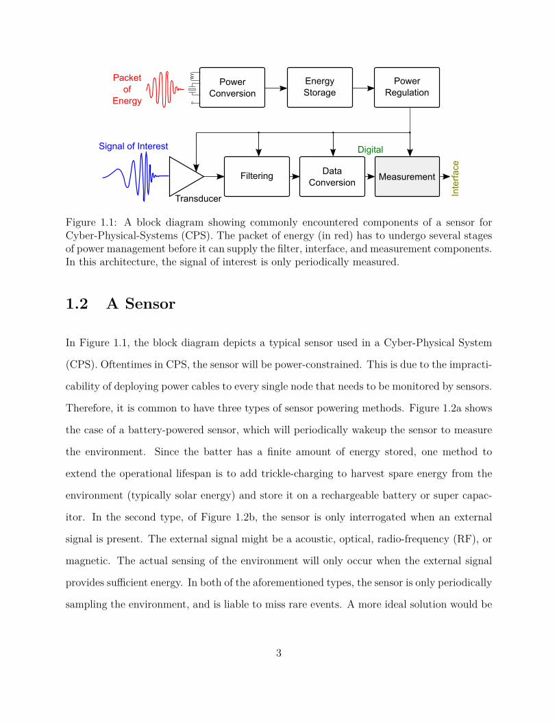
Figure 1.1: A block diagram showing commonly encountered components of a sensor forCyber-Physical-Systems (CPS). The packet of energy (in red) has to undergo several stagesof power management before it can supply the filter, interface, and measurement components.In this architecture, the signal of interest is only periodically measured.
1.2 A Sensor
In Figure 1.1, the block diagram depicts a typical sensor used in a Cyber-Physical System
(CPS). Oftentimes in CPS, the sensor will be power-constrained. This is due to the impracti-
cability of deploying power cables to every single node that needs to be monitored by sensors.
Therefore, it is common to have three types of sensor powering methods. Figure 1.2a shows
the case of a battery-powered sensor, which will periodically wakeup the sensor to measure
the environment. Since the batter has a finite amount of energy stored, one method to
extend the operational lifespan is to add trickle-charging to harvest spare energy from the
environment (typically solar energy) and store it on a rechargeable battery or super capac-
itor. In the second type, of Figure 1.2b, the sensor is only interrogated when an external
signal is present. The external signal might be a acoustic, optical, radio-frequency (RF), or
magnetic. The actual sensing of the environment will only occur when the external signal
provides sufficient energy. In both of the aforementioned types, the sensor is only periodically
sampling the environment, and is liable to miss rare events. A more ideal solution would be
3

that of Figure 1.2c, in this case the environmental signal to be measured is providing suffi-
cient energy to complete a sensing task. Although this would be a relatively simple task if
the signal of interest were solar (an intense light source), it becomes exceedingly non-trivial
when attempting to sense smaller signals like mechanical power across piezoelectrics, RF
coupled to an antenna, or even photovoltaics being activated with a weak light source. Note
that in this solution of using the input stimuli as the energy source, the top row of blocks
in Figure 1.1 are eliminated from consideration, simplifying the design requirements and
minimizing the wasted energy that would have been lost in the energy conversion, storage,
and regulation stages.
EnvironmentSensor
Sense
Energy Storage
Po
we
r
Environment
(a)
EnvironmentSensor
Sense
External Energy
Optical
Po
we
r
(b)
EnvironmentSensor
Sense
Energy
(c)
Figure 1.2: Showing three types of sensors, (a) passive that will periodically wake up tomake measurements, (b) energy harvesting that needs to scavenge enough energy from theenvironment before making periodic measurements, (c) self-powered, continuous sensor inwhich the stimuli to measure is sufficient energy.
4

1.2.1 Transduction
The first stage of a sensor that is making a measurement of its environment is to couple the
signal of interest with a transducer. There may be some confusion between the differences
of a sensor and transducer, luckily The American National Standards Institute (ANSI) has
given the following definition for a transducer.
A device which provides a usable output in response to a specific measurand.
It seems then, that many devices would thus be eligible as transducers. In the context of this
work, a transducer is assumed to be a device that merely converts any observable energy into
an electrical signal. Thus, when discussing a “sensor” in this work, it can be assumed that
everything beyond the transduction stage takes place in the electrical domain. For example,
if the signal of interest is optical, a photovoltaic cell could be used to convert photons into
electrons. Similarly, when sensing strain, a piezoelectric might be sufficient to generate an
electric field to couple to the sensor. In Table 1.2.1, four common sources are listed with their
respective operating frequency, open circuit voltage, and source impedance. The electrical
characteristics of each source, when coupled to a typical transducer for that source, will need
to be considered for the downstream blocks after transduction.
1.2.2 Filter
After getting the signal from the transducer in the form of an electrical signal, a typical
step is to have protection circuitry. This could come in the form of resistors to limit inrush
current, capacitors to smooth out ripples, or diodes to prevent overvoltage. Resistors and
capacitors (and less commonly on older CMOS processes, inductors) could also be used to
5

Table 1.2: Electrical Properties of Transducers for Different Power Sources
SourceTypical Open-
Circuit Voltage VOC
OperatingFrequency fS
Typical SourceImpedance ZS
Optical 0.5 – 5 V DCVariable ImpedanceLow kΩ – 10s of kΩ
Thermal 10 mV – 10 V DCResistive Impedance
1 – 100s of Ω
Vibration 10 – 50 V 0.1 Hz – 1 kHzCapacitive impedance
10s of kΩ – 100 kΩ
RF & Inductive 100 mV – 5 V 100 kHz – 5 GHzInductive Impedance
Low kΩ
do filtering of the signal in the frequency domain. Perhaps the environment generate many
spurious high-frequency signals that are not of particular interest for a given application. A
good sensor would be able to filter out the noise and leave the observer with a measurement
that has a high signal-to-noise ratio.
1.2.3 Data Conversion
In the analog world, the data conversion step is not necessary before measurement. For
certain types of interfacing, a data conversion block may appear between the measurement
and interface components of Figure 1.1.
1.2.4 Measurement
Perhaps the key component in the sensor system of Figure 1.1 after the transducer. This stage
will store the transduced (i.e. converted to electrical) and filtered signal-of-interest for an
observer to collect through the interface stage. Depending on the sensor, this measurement
6

block might be a simple capacitor that loses its memory almost as quickly as it stores it.
In applications demanding rapid interfacing, this is not an issue. Recognizing that many
CPS applications would have slower consumption of their data than in high-throughput,
mains driven sensors, this block might be better served by a non-volatile memory that
retains the information for later retrieval by an observer. For most commercial sensors, this
measurement memory would be implemented using NAND flash memory or other digital
storage, either within the sensor or on an external memory chip.
1.2.5 Interface
Pow
er
(W)
103 10-21100 10-3 10-6 10-9 10-12 10-15 10-18
Therm
al
Nois
e
GP
SS
ignal
CM
OS
Inve
rter
Hum
an
Cell
MC
U
Sle
ep
Pass
ive
RFID
AR
MB
lueto
oth
Lapto
ps
Thermal Energy
Embedded
Sensor
Gradiants
Radio-frequency Signal
Embedded Sensor
UplinkDownlink
Mechanical Strain
Embedded
Sensor
Power
Monitor
Figure 1.3: Illustrating approximate energy requirements for certain processes. In the tophalf of the figure, three methods of energy-harvesting are shown with typical target drivingpower.
When an observer wishes to retrieve the information that was measured by a sensor, they
do so through an interface. This could be any modality such as wires, RF transmissions, a
buffered voltage, or even acoustic [7]. When considering the interface method, it is important
to keep in mind the required energy level for various processes. From Figure 1.3, the lower
end of digital interface appears to be in the µW range.
7

1.3 Objectives and Contributions
Co
st (U
SD
)
100
10-1
10-2
101
102
1985 1990 1995 2000 2005 2010 2015Year
A million silicon transistors
Concrete pavement (1000 cm3)
Structural concrete (1000 cm3)
Structural steel (lbs)
Passive RFID tag
Figure 1.4: A plot that shows an increase in construction material cost versus a decreasein cost to implement silicon. In recent times, the cost of adding a million transistors to apound of construction material appears to be a small fraction.
One of the consequences of the celebrated Moore’s law [8] is that the cost of fabricating
silicon integrated circuits (ICs) has reduced exponentially over the last several decades, as
shown in Fig. 1.4. Nowhere has this trend manifested more profoundly than in the area
of radio-frequency identification (RFID) tagging technology where the volume production
cost of a single tag is less than ten cents [9]. If compared against the price trend of typical
construction and structural materials (e.g. concrete or steel) during the same period, it can
be seen from Fig. 1.4 that it is now economically viable to embed an RFID tag within every
pound of concrete brick or inside every square foot of a large structure such as pavement
highway, buildings, or multi-span bridges. In the past decade since the data points on the
figure were last updated, Intel has claimed to maintain the same rate of reduction in cost per
8

Self-Powered Sensor
Bridges
Buildings
Highways
NFC
Radar
UHF
WiFi
802.11
3G/4G
Mobile
Satellite
Link
Cloud
Computing
ISM
Test-beds Sensors
- Self-powered health
monitoring sensors
- Hybrid energy scavenging
RFID processors
Structural Health
Monitoring
- Data aggregation,
analytics, and damage
prediction
- Structural forensics
- Buildings
- Highways
- Bridges
- Levees
- Pipes
Structural
Forensics
Data Interpretation
Figure 1.5: Overview of the infrastructural Internet of Things framework, green backgroundshows potential CPS applications, the red background is for the enabling technology, andblue is for data interpretation by domain experts. The self-powered sensors are mocked upas red dots.
transistor, and steel prices have continued to trend up leading to another order of magnitude
in price difference. If these tags are endowed with sensing capabilities, these sensors could
form a part of the infrastructural Internet-of-Things (i-IoT) vision for monitoring health of
civil infrastructure (as shown in Fig. 1.5) where millions of embedded sensors continuously
monitor the mechanical usage of the structure and the usage data could then be used for
condition-based maintenance of the structure. An i-IoT deployment could potentially lead
to significant savings and prevention of hazards and catastrophic failures. For instance
in the US, each state highway agency currently spends several million dollars per year to
inspect highway structures and bridges for damage. These inspection methods are reactive
9
in nature and require significant personnel time or use of costly capital equipment. Also, an
infrastructure monitoring network as envisioned in Fig. 1.5 could be used to quickly assess
damage to infrastructure after a seismic event such that maintenance procedure could be
directed to the areas that need immediate attention. By being proactive with maintenance,
society could reduce the chances of a catastrophic failure.
Po
we
r (W
atts)
Feature Size (m)10-6 10-4 10-2 100
10-20
10-15
10-10
10-5
100
105
PVDF
PZT-5H
Target (>nW)
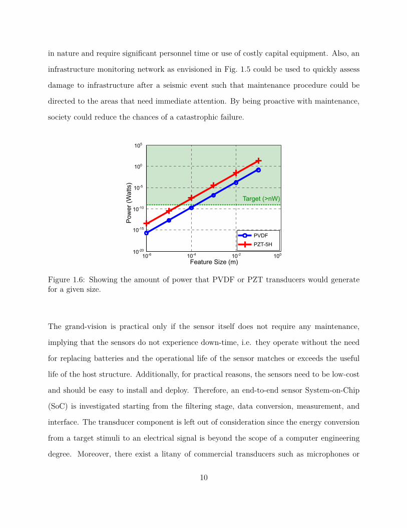
Figure 1.6: Showing the amount of power that PVDF or PZT transducers would generatefor a given size.
The grand-vision is practical only if the sensor itself does not require any maintenance,
implying that the sensors do not experience down-time, i.e. they operate without the need
for replacing batteries and the operational life of the sensor matches or exceeds the useful
life of the host structure. Additionally, for practical reasons, the sensors need to be low-cost
and should be easy to install and deploy. Therefore, an end-to-end sensor System-on-Chip
(SoC) is investigated starting from the filtering stage, data conversion, measurement, and
interface. The transducer component is left out of consideration since the energy conversion
from a target stimuli to an electrical signal is beyond the scope of a computer engineering
degree. Moreover, there exist a litany of commercial transducers such as microphones or
10

piezoelectrics made of polyvinylidene difluoride (PVDF) and lead zirconate titanate (PZT)
that could provide sufficient energy to have a self-powered sensor as outlined in Figure 1.2c.
From readily available data, the power levels of PVDF and PZT for a given area are shown
in Figure 1.6 and verify that as long as the sensor can operate in the nW range a minimally
sized piezoelectric would suffice.
1.3.1 Filter: Speaker Recognition
The problem of developing a filter is considered in isolation to the other components. A
general overview of filter analysis is presented in Chapter 2, followed by a current-mode
biquad filter implemented in hardware and verified on a speaker recognition task presented in
Chapter 3. The lessons learned in this endeavor are folded into the other sensor components
that were developed in parallel.
1.3.2 Data Conversion & Measurement: Piezolectric-Floating-Gate
Table 1.3: Comparison for Piezoelectric Harvesting Circuit Efficiency.
Ref. Method Resonant f Efficiency (%) Max Power
[10] DSSH 105.3 Hz 40 5.5 mW
[11] SSHI 1 kHz 20.2 <400 µW
[12] Bias flip 225 Hz 87.5 <70 µW
[13] Synchronous bridge rectifier 125 Hz 50–70 8 µW
[14] Rectifier 301 Hz 64 25 µW
[15] Switched-inductor 100 Hz 41.7 30 µW
[16] Adaptive feedback 250 Hz 60 300 µW
11

For the target application of CPS for Structural-Health Monitoring (SHM), monitoring strain
levels through piezoelectrics is one of the most impactful. Table 1.3 shows the maximum
power and efficiency of several methods for harvesting energy from piezoelectrics. These re-
sults demonstrate the potential for implementing a Figure 1.2c style sensor since there in an
abundance of energy. The data conversion and measurement components are implemented
using a piezoelectric-floating-gate (PFG) circuit that allows the direct coupling of the analog
electrical energy from a piezoelectric to a data-logging floating-gate [17, 18]. The core tech-
nology was previously reported under laboratory testing conditions [19, 20]. A SoC version
of the core technology was developed and testing under rigorous conditions as reported in
Chapter 4, and several trials were conducted in harsh, real-world conditions. The lessons
learned during the filtering component testing are merged with the PFG in Chapter 5.
1.3.3 Interface: Wireless Interrogation Techniques
Taking the core technology out of the laboratory and test it in the real world required the
removal of any wired dependencies (external voltage references, input commands, and output
data). To this end, several wireless technologies from self-powered backscattering to active
RF transmission are explored in Chapter 6.
12

Chapter 2
Analysis of Filters
2.1 Linear
When dealing with filters, it is often assumed that one may operate in the “linear” region of
the filter. From a mathematical perspective, one may state that a filter is linear as long as
it can satisfy the following conditions:
Additive for any two inputs x1(t) and x2(t),
F [x1(t) + x2(t)] = F [x1(t)] + F [x2(t)] (2.1)
Homogeneous for any input x(t) and constant α,
F [αx(t)] = αF [x(t)] . (2.2)
If both conditions are met, the filter F is “linear”; under such an assumption, one may
simplify the small signal analysis to make first-order approximations of a filter’s behavior.
To demonstrate a linear and nonlinear function, consider first this function y(t) = t2x(t).
13

Is it additive?
F [x1 + x2] = t2 (x1(t) + x2(t)) (2.3)
= t2x1(t) + t2x2(t) (2.4)
= F [x1(t)] + F [x2(t)] , Yes (2.5)
Is it homogeneous?
F [αx(t)] = t2αx(t) = αt2x(t) (2.6)
= αF [x(t)] , Yes (2.7)
Thus, one may conclude that the function y(t) = t2x(t) is linear. On the other hand, a
function such as y(t) = x2(t) would be nonlinear since
It is not additive,
(x1(t) + x2(t))2 = x2
1(t) + 2x1(t)x2(t) = x22(t) 6= x2
1(t) + x22(t) (2.8)
nor homogeneous (unless α ∈ 0, 1)
(αx(t))2 = α2x2(t) 6= αx2(t) (2.9)
14

Figure 2.1: A schematic representation of a biquad filter implementation using transconduc-tance amplifiers.
2.1.1 Derivation of Gm-Ciquad Filter Transfer Function
Given a filter architecture as in Fig. 2.1, the linear transfer function can be approximated
using the knowledge that the transfer function of each transconductance amplifier is
Iout = gm ∗ (V+ − V−) . (2.10)
For a small signal analysis, we treat the DC references Vref1 and Vref2 as virtual ground, then
the three output currents from the transconductance amplifiers is:
I1 = gm1Vin, (2.11)
I2 = gm2 (Vx − Vbp) , (2.12)
I3 = gm3 (0 − Vbp) . (2.13)
15

The voltage Vx is determined by the capacitance at the node being charged by the output
current from gm2 since the inputs of the transconductance draw essentially no current. That
is,
Vx =(
1
sC2
)
gm3 (−Vbp) , (2.14)
where 1sC2
is the Laplace transform for the node Vx. Similarly, the node Vbp is described as
Vbp = ZC1(I1 + I2) (2.15)
=(
1
sC1
)(
gm1Vin + gm2 (−Vbp)(
1 +gm3
sC2
))
(2.16)
= Vin
(
gm1
sC1
) [
1 +gm2
sC1
+gm2gm3
s2C1C2
]
−1
. (2.17)
This leads to a transfer function of
H(s) =Vbp
Vin
=(
gm1
sC1
) [
1 +gm2
sC1
+gm2gm3
s2C1C2
]
−1
(2.18)
=s(
gm1C2
gm2gm3
)
s2(
C1C2
gm2gm3
)
+ s(
C2
gm3
)
+ 1(2.19)
2.2 Nonlinear
In the real world, one would be hard-pressed to find a linear filter, especially if an active
filter is being considered. In a simple sense, nonlinearity is experienced when the output of
a system does not vary in direct proportion to its input, e.g. a diode. More strictly, one
need only to check if the system is linear using the criterion from the previous section, if it
is not linear then one may state that it is nonlinear. When dealing with active filters, the
nonlinearity of the core amplifiers can dictate the performance of the filter system. There
16

are a multitude of nonlinearities that can come into play based on magnitude or frequency
of the system as outlined in the Table 2.1.
Table 2.1: Types of Nonlinearity
Magnitude FrequencySaturation Jump resonanceDead zone Limit cycleFriction HarmonicsBacklash Chaotic behavior
Relay Self excitation
For the purposes of this dissertation, the consideration of saturation nonlinearity is sufficient.
2.2.1 Saturating Nonlinearity
A common method for approximating the nonlinearity in a system is to use a describing
function, in this subsection, the derivation of a describing function for saturation is presented.
Given the characteristic curve in Fig. 2.2, with an input excitation of
X(t) = X sin(ωt), (2.20)
the output is thusly defined as:
Y (t) = AX sin(ωt), for 0 ≤ ωt ≤ β (2.21)
Y (t) = As, for β ≤ ωt ≤ π − β (2.22)
Y (t) = AX sin(ωt), for (π − β) ≤ ωt ≤ π. (2.23)
17

Figure 2.2: The characteristic curve of a saturating nonlinearity and the approximate outputfor a sinusoidal input.
When considering the Fourier series,
f(x) ≈ a0
2+
∞∑
n=1
an cos(
2π
Lnx)
+ bn sin(
2π
Lnx)
, (2.24)
the coefficients can be calculated as
a1 =1
π
∫ 2π
0y(t) cos(ωt) d(ωt) (2.25)
= 0 (2.26)
18

b1 =1
π
∫ 2π
0y(t) sin(ωt) d(ωt) (2.27)
=4
π
∫ π/2
0y(t) sin(ωt) d(ωt) (2.28)
=1
π
[
∫ β
0AX sin2(ωt) d(ωt) +
∫ π/2
βAs sin(ωt) d(ωt)
]
(2.29)
=4A
π
[
Xβ
2− X
4sin(2β) + s cos(β)
]
(2.30)
=2AX
π
[
β + 2S
Xcos(β) − sin(β) cos(β)
]
. (2.31)
With the further knowledge that
AX sin(ωt) = As, if ωt = β (2.32)
⇒ sin =As
AX(2.33)
⇒ β = sin−1
(
s
X
)
, (2.34)
The coefficient b1 is further simplified to
b1 =2AX
π
[
sin−1
(
s
X
)
+ 2S
Xcos
(
sin−1
(
s
X
))
− sin(
sin−1
(
s
X
))
cos(
sin−1
(
x
X
))]
(2.35)
=2AX
π
sin−1
(
s
X
)
+(
s
X
)
√
1 −(
s
X
)2
. (2.36)
19

Further, the phase angle of the describing function is ∠ tan−1(
a1
b1
)
= ∠0°. Thus, the final
describing function, N = b1
X∠0° is
2A
π
sin−1
(
s
X
)
+(
s
X
)
√
1 −(
s
X
)2
∠0°. (2.37)
2.3 Boundary Curves
For a simple filter system that is comprised of a linear filter block and a nonlinear saturating
element that depends on the input magnitude and frequency, as depicted in Fig. 2.3, we can
gain an insight into how the saturating nonlinearity will affect a filter system’s response.
r+-
x yG(jω)f(x)
Figure 2.3: A block diagram of a simple nonlinear filter feedback system, with linear filterG(jω) and nonlinearity f(x).
To begin the analysis, we must make some assumptions, namely: (a) the system shown
in Fig. 2.3 is stable; (b) the linear block G(jω) is frequency dependent and amplitude in-
dependent; (c) the nonlinearity f(x) is single-valued, odd, continuously differentiable, and
frequency independent; (d) higher harmonics are suppressed by G(jω) and f(x) creates neg-
ligible harmonics [21, 22, 23]. We assume that the input signal is sinusoidal, as before (2.20).
20

Based on the aforementioned assumptions, the resulting output at x should be periodic and
of the form:
x(t) = Xsin(ωt + φ). (2.38)
To evaluate the nonlinear feedback system that is driven by a periodic input, without resort-
ing to complicated nonlinear analysis, the describing function (2.37) is written in the general
form [24, 25, 26]
N(X) = ξ(X) + jη(X) (2.39)
Also without delving into the specific transfer function, H(jω), of the linear filter block, the
general form is used.
H(jω) =1
G(jω)= hr(jω) + jhi(jω) (2.40)
Equations (2.41-2.43) show the analysis in the Laplace domain for finding the output at x,
as it relates to the input r.
X(s) = R(s) − G(s)Y (s) (2.41)
Y (s) = N(s)X(s) (2.42)
X(s) = R(s) − N(s)G(s)X(s) (2.43)
21

Using the result from (2.43) and plugging in (2.39) and (2.40) to find the closed-loop transfer
function gives:
Xejθ
Rejθ=
1
1 + N(X)G(jω)(2.44)
=1
1 + N(X)H−1(jω)(2.45)
=
(
H(jω) + N(X)
H(jω)
)
−1
. (2.46)
Squaring (2.46) will remove the dependence on complex terms and will result in the amplitude
of the transfer function; i.e.,
(
R
X
)2
=(hr(ω) + ξ(X))2 + (hi(ω) + η(X))2
h2r(ω) + h2
i(ω). (2.47)
Since we have assumed that f(x) will be single-valued, the condition for nonlinear behavior to
occur is dependent on the input signal. For a constant input frequency (dω = 0), the input
amplitude of r will correspond to the amplitude at x when the describing function (2.39) is
continuously differentiable, and the point of the first jump will occur at ∂R/∂E|dω=0 = 0,
since a change in output does not require a change of the input. Previous research [27, 28,
29, 30] has shown that a sufficient condition for the sudden change in output amplitude and
phase is as follows:
∂R
∂X
∣
∣
∣
∣
∣
dω=0
≤ 0. (2.48)
Evaluating the partial derivative of (2.47) requires solving the following expression:
2(h2r + h2
i)R∂R
∂X= X2((hr + ξ(X))2 + (hi + η(X))2). (2.49)
22

The partial derivative of X2(hr + ξ(X))2 can be solved independently as:
∂X2(hr + ξ(X))2
∂X= X2
(
∂
∂X(hr + ξ(X))2
)
+(hr + ξ(X))2
(
∂
∂X(X2)
)
(2.50)
= X2
[
2(hr + ξ(X))
(
∂
∂Xhr + ξ(X)
)]
+2X(hr + ξ(X))2 (2.51)
= 2X2(hr + ξ(X))∂ξ
∂X
+2X(hr + ξ(X))2. (2.52)
A result similar to (2.52) can be found for the hi and η(X) terms, both of which can be
applied to (2.49) to write the partial derivative as:
2(h2r + h2
i)R∂R
∂X= 2X
[
(hr + ξ(X))X∂ξ
∂X
+(hi + η(X))X∂η
∂X+ (hr + ξ(X))2
+(hi + η(X))2]
(2.53)
Furthermore, by using the algebraic manipulation (2.54), the equation in (2.53) can be
rewritten as (2.55).
(hr + ξ(X))X∂ξ
∂X+ (hr + ξ(X))2 =
(
hr + ξ(X) +X
2
∂ξ
∂X
)
−(
X
2
∂ξ
∂X
)2
(2.54)
23

(h2r + h2
i)R∂R
∂X= X
−(
X
2
∂ξ
∂X
)2
−(
X
2
∂η
∂X
)2
+
(
hr + ξ(X) +X
2
∂ξ
∂X
)
+
(
hi + η(X) +X
2
∂η
∂X
)]
(2.55)
= X
[
−(ξ − γ1)2 + (η − γ2)
2
4
+
(
hr +ξ + γ1
2
)2
+(
hi +η + γ2
2
)2]
(2.56)
(2.57)
To simplify the equation (2.55) to (2.56), the terms from (2.58) and (2.59) were used.
γ1 = ξ + X∂ξ
∂X(2.58)
γ2 = η + X∂η
∂X(2.59)
Taking care to define variables ρ, p1, and p2, such that ρ relates to a radius, while p1 and p2
define a center point of the form p1 + jp2, one will find that,
ρ =1
2
√
(ξ − γ1)2 + (η − γ2)2 (2.60)
p1 =−1
2(ξ + γ1) , p2 =
−1
2(η + γ2). (2.61)
24
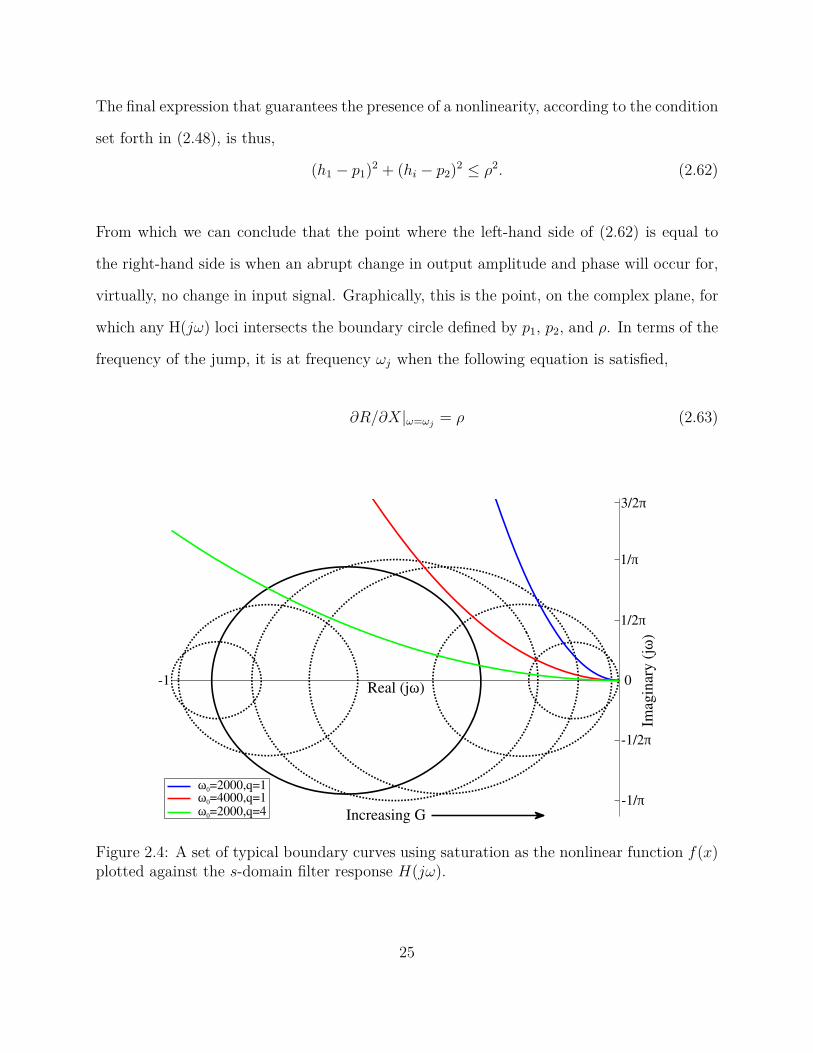
The final expression that guarantees the presence of a nonlinearity, according to the condition
set forth in (2.48), is thus,
(h1 − p1)2 + (hi − p2)
2 ≤ ρ2. (2.62)
From which we can conclude that the point where the left-hand side of (2.62) is equal to
the right-hand side is when an abrupt change in output amplitude and phase will occur for,
virtually, no change in input signal. Graphically, this is the point, on the complex plane, for
which any H(jω) loci intersects the boundary circle defined by p1, p2, and ρ. In terms of the
frequency of the jump, it is at frequency ωj when the following equation is satisfied,
∂R/∂X|ω=ωj= ρ (2.63)
Imaginary (jω)
-1/π
-1/2π
0
1/2π
1/π
3/2π
-1
ω0=2000,q=4ω0=4000,q=1ω0=2000,q=1
Real (jω)
Increasing G
Figure 2.4: A set of typical boundary curves using saturation as the nonlinear function f(x)plotted against the s-domain filter response H(jω).
25

It should be noted that each p1, p2 pair will have a corresponding ρ value; when evaluating
the intersection points graphically, there will be several circles that could intersect H(jω).
Because f(x) is assumed to be single-ended, these boundary circles will be symmetric with
respect to the real axis. A saturating nonlinearity, which has ordinates equal to zero for
all points of interest, will create boundary curves of the type shown in Fig. 2.4, using the
linear filter responses shown in Fig. 2.5. An estimated nonlinear filter response using the
linear filters from Fig. 2.5 and the boundary curve shown in solid black in Fig. 2.4 is given
in Fig. 2.6.
5000400030002000Frequency (Hz)
10000-20
-15
-10
Magnitude (dB)
-5
0
ω0=2000,q=4ω0=4000,q=1ω0=2000,q=1
Figure 2.5: The linear filter component (G(jω) of Fig. 2.3) response from the analysis pre-sented in Fig. 2.4.
Since the condition (2.62) is ≤, jumps may also occur when the H(jω) trace is within the
boundary of a circle. Considering a transfer function of a bandpass filter, a higher quality
factor will require a smaller input amplitude to drive a system to become nonlinear, as is
shown in Fig. 2.4 [31]. The filter tuned to a higher center frequency of 4,000 rad/s was close
26

50003000Frequency (Hz)
1000 2000 40000
0.2
0.4
0.6
0.8
1
Norm
aliz
ed A
mplitu
de
ω0=2000,q=4ω0=4000,q=1ω0=2000,q=1
Figure 2.6: The estimated nonlinear filter response of Fig. 2.3 when considering a saturationnonlinearity as f(x) and the linear filter G(jω) as given in Fig. 2.5.
to the boundary curve, but did not pass through it, therefore it begins to present a shark-
fin-like response, but does not exhibit the nonlinearity of jump resonance. The conditions
set forth in the preceeding analysis do not guarantee the existence of jump resonance (or
other nonlinearities), rather the conditions must be met if the nonlinearity is to exist.
27

Chapter 3
Jump Resonance
3.1 Motivation
Jump resonance is a phenomenon observed in nonlinear circuits where the output can ex-
hibit abrupt variations for a continuous, well-behaved, periodic input signal [27, 32]. The
phenomenon has been observed and studied extensively in nonlinear control systems and in
analog filters [31] where jump-resonance leads to a hysteresis behavior when the frequency of
the input signal is varied. This is illustrated in Fig. 3.1 where the output signal magnitude is
not only a function of the input signal frequency, but also a function of the direction of the
frequency sweep. Thus, for frequencies within the hysteresis band defined by ω1 < ω < ω2,
the magnitude of the output signal could have two possible magnitudes depending on the fre-
quency trajectory. Current-mode analog-filters that are biased in weak-inversion are typically
susceptible to artifacts due to jump-resonance. This is due to the fact that sub-threshold
biasing hinders the filter’s inherent inability to respond rapidly to the given input signal [33].
This may be because the magnitude of the input signal exceeds the filter’s linear range, or
that the frequency of the input signal varies more quickly than the slewing ability of the
filter’s active circuit elements.
28

Figure 3.1: Illustration of a band-pass response exhibiting jump-resonance and its compari-son with a conventional band-pass response.
Figure 3.2: Spectrogram of a sample speech utterance showing frequency or formant trajec-tories.
In the design of auditory front-ends (AFEs) like the silicon cochlea, such a filter response
has been considered undesirable and several methods have been proposed to predict and
remedy jump-resonance artifacts [33, 27]. However, the hysteretic response with respect to
the direction of the frequency sweep could be used as a computational tool for encoding
formant trajectory in speech signal. Formants in speech signal correspond to the resonant
frequencies of the vocal tract, in particular, when vowels are pronounced. Fig. 3.3(b) shows
29

(a)
(b)
(c)
Figure 3.3: (a) Sample format trajectories during a phonetic utterance in English language.For the sample trajectory: (b) response expected from a conventional band-pass filter; and(c) response expected from the filter exhibiting jump-resonance for the sample trajectories.
the location of three formant frequencies (F1, F2 and F3) on a spectrogram. Trajectory of
formants over time (as shown in Fig. 3.3(b)) are particularly relevant for speaker recognition
because they are indicator of the mechanical dynamics of the vocal tract and that these
signatures are robust to corruption by ambient noise [35]. For example, Fig. 3.4 and Fig. 3.5
show example trajectories of the formants F1 and F2 corresponding to different English
vowels and corresponding to male and female speakers. Conventional auditory front-ends
for speaker recognition extract formant trajectories by complementing the output of the
filter-banks by ∆, or velocity features, and by ∆∆, or acceleration features, which have been
hypothesized as being capable of capturing infrasonic signatures [36]. Using digital signal
processing, the process of extracting ∆ and ∆∆ features entails a linear and a quadratic
30
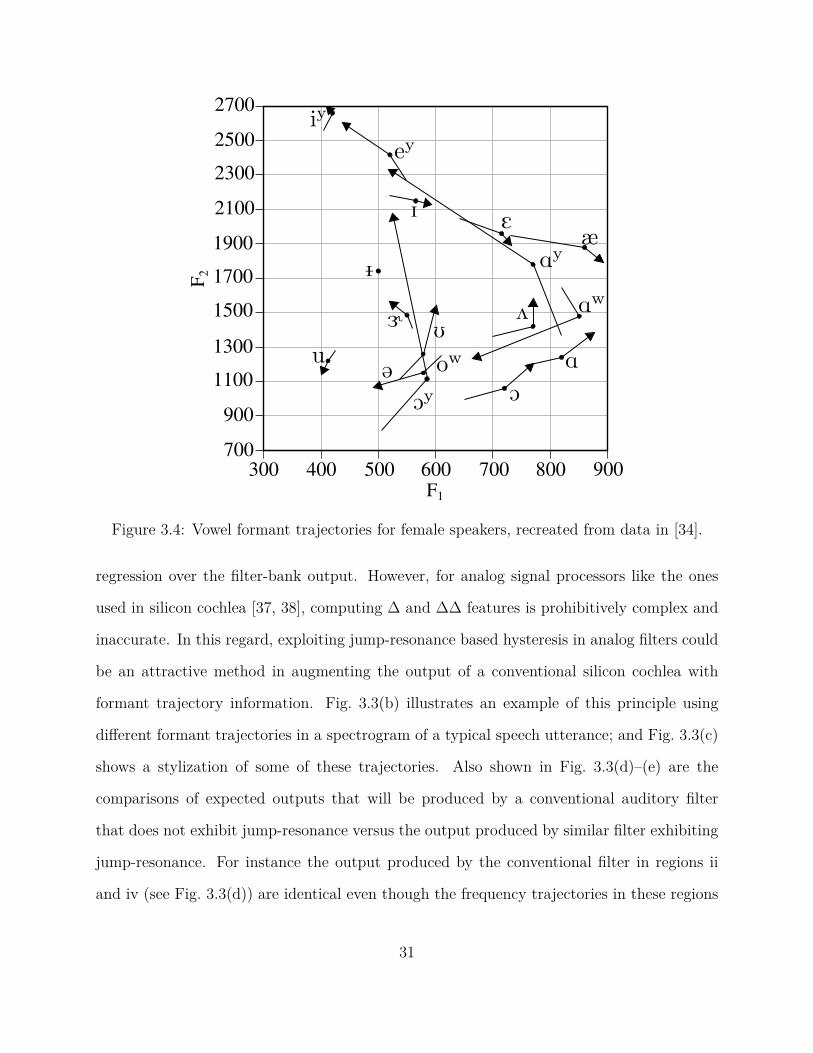
Figure 3.4: Vowel formant trajectories for female speakers, recreated from data in [34].
regression over the filter-bank output. However, for analog signal processors like the ones
used in silicon cochlea [37, 38], computing ∆ and ∆∆ features is prohibitively complex and
inaccurate. In this regard, exploiting jump-resonance based hysteresis in analog filters could
be an attractive method in augmenting the output of a conventional silicon cochlea with
formant trajectory information. Fig. 3.3(b) illustrates an example of this principle using
different formant trajectories in a spectrogram of a typical speech utterance; and Fig. 3.3(c)
shows a stylization of some of these trajectories. Also shown in Fig. 3.3(d)–(e) are the
comparisons of expected outputs that will be produced by a conventional auditory filter
that does not exhibit jump-resonance versus the output produced by similar filter exhibiting
jump-resonance. For instance the output produced by the conventional filter in regions ii
and iv (see Fig. 3.3(d)) are identical even though the frequency trajectories in these regions
31
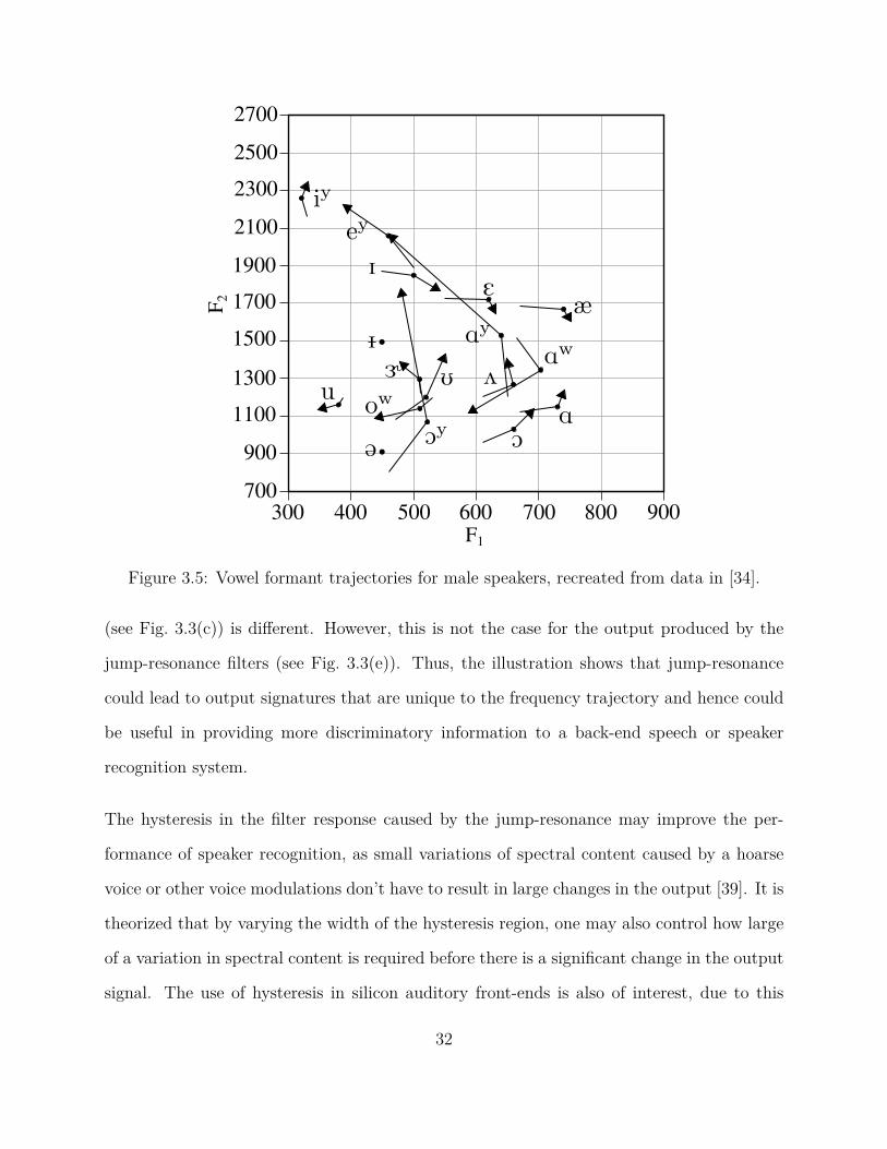
Figure 3.5: Vowel formant trajectories for male speakers, recreated from data in [34].
(see Fig. 3.3(c)) is different. However, this is not the case for the output produced by the
jump-resonance filters (see Fig. 3.3(e)). Thus, the illustration shows that jump-resonance
could lead to output signatures that are unique to the frequency trajectory and hence could
be useful in providing more discriminatory information to a back-end speech or speaker
recognition system.
The hysteresis in the filter response caused by the jump-resonance may improve the per-
formance of speaker recognition, as small variations of spectral content caused by a hoarse
voice or other voice modulations don’t have to result in large changes in the output [39]. It is
theorized that by varying the width of the hysteresis region, one may also control how large
of a variation in spectral content is required before there is a significant change in the output
signal. The use of hysteresis in silicon auditory front-ends is also of interest, due to this
32

similarity to the mechanical hysteresis phenomenon observed in animal cochlea. Research
conducted on gerbils has revealed that the cochlea exhibits a nonlinear transducer function
that exhibits a sigmoid-shaped hysteresis loop with counterclockwise traversal [40]. Further
research has also suggested that the transducer nonlinearity in humans would be similar
or possibly more pronounced than the results obtained from gerbils [41]. There are many
studies that indicate biological systems have jump resonance hysteresis, and they serve as an
inspiration to employed similar tactics in silicon filters, with the goal of improving speaker
recognition system performance.
3.2 Jump Resonance Criteria for GmCilter
A general criteria that must be satisfied for the existence of a jump resonance nonlinearity
considering an amplifier with a saturating nonlinearity was presented earlier in Section 2.3,
based on the simple filter of Fig. 2.3. Here, we present a derivation of the jump resonance
criteria in a Gm-C filter of Fig. 3.6.
In this configuration, the biquad filter consists of linear transconductors with transconduc-
tances gm1, gm2 and gm3 and a transfer function, as dereived earlier in 2.1.1, of
G(jω) =Vo(s)
Vi(s)=
Gω0
Qs
s2 + ω0
Qs + ω0
2. (3.1)
The center-frequency (ω0), quality-factor (Q) and filter-gain G can be expressed in terms of
gm1,gm2 and gm3 as
Q =
√
gm2
gm3
(3.2)
ω0 =
√gm2 × gm3
C(3.3)
33

Figure 3.6: A schematic representation of a biquad filter implementation using transconduc-tance amplifiers.
G =gm1
gm3
. (3.4)
As we explained in the previous chapter, any practical amplifier, i.e. transconductors, will ex-
hibit a nonlinear saturating response due to their finite input-output dynamic range. There-
fore, a closed-form analysis of the circuit presented in Fig. 3.6 becomes troublesome and an
approximation using graphical techniques is preferred; here we use the describing function
approach from literature [24, 25, 26]. The assumption that only gm2 exhibits a saturating
nonlinearity is made to simplify the analysis, and the second-order system transfer function
of (3.1) is decomposed into the feedback architecture of Fig. 3.7. Thus, Fig. 3.6 is modeled
as a linear filter combined with a nonlinear element gm2, which conforms to a classical topol-
ogy encountered in non-linear control systems. The linear portion of the architecture is a
low-pass filter that attenuates higher-order harmonics generated by the non-linear element.
Note that when gm2 is assumed to be linear, the system transfer function reduces exactly
34

to (3.1).
Figure 3.7: Signal-flow diagram for Fig. 3.6 to analyze nonlinear artifacts in the biquad filter.
The describing function method linearizes the operation of gm2 in the frequency domain,
where the dynamics of the system can be analyzed at a specific frequency ω. Let the signal at
the input of the transconductor gm2 be denoted by Vbp sin(ωt); the output current be denoted
by Ix sin ωt; and the signal at the input of the system be denoted by Vin sin (ωt + β). Here
we have assumed that the non-linearity in gm2 is frequency independent and hence does not
introduce any phase-shifts. Therefore, Ix and Vbp are related through the non-linearity as:
Ix
Vin
= N(Vbp)Vbp
Vin
, (3.5)
where N(Vbp) is the frequency independent describing function and is only a function of
signal amplitude Vbp.
Also, Ix, Vbp and Vin are related to each other through the linear portion of the system as
Vbp
Vin
=
∣
∣
∣
∣
∣
gm1
gm3 + jωC
∣
∣
∣
∣
∣
√
√
√
√1 −(
Ixgm3
VinωCgm1
sin(
θ1 − π
2
)
)2
−∣
∣
∣
∣
∣
gm1
gm3 + jωC
∣
∣
∣
∣
∣
Ixgm3
VinωCgm1
cos(
θ1 − π
2
)
(3.6)
35

A more detailed look into the derivation of this relationship is in the subsequent subsection.
To get an insight on how jump-resonance is introduced by the non-linearity due to gm2,
we will assume a simplistic saturation non-linear model shown in Fig. 2.2. The describing
function for the model is well known [42, 43, 44] and can be expressed as:
N(Vbp) =
gm2 , Vbp ≤ δ
(
gm2
π
)
(2α + sin(2α)) , Vbp > δ
(3.7)
where α = sin−1
(
δ
Vbp
)
. (3.8)
The loci corresponding to (3.6) is plotted in Fig. 3.8 as the frequency ω is varied. Also plotted
are the curves corresponding to (2.37), for the case when gm2 is linear and for the case when
gm2 exhibits a saturating non-linearity corresponding to Fig. 2.2. The intersection between
the two curves represents the solution (Ix, Vbp) obtained at a frequency ω. For instance,
the point P1 is the system solution at frequency ω1. As the frequency is increased the
intersection point traverses P2 and P3. For the linear system, as the frequency is increased
the magnitude of the output reaches a maximum at P4 (frequency ω4) and then decreases
as the frequency is increased. This response is illustrated in the magnitude plot shown in
Fig. 3.9. The response is typical of a band-pass biquad filter with center-frequency ω4. For
the non-linear system, the initial system trajectory is similar to that of the linear system
but deviates from P3 as equations (3.6) and (2.37) become tangential to each other. At this
point, the system exhibits a jump to the solution Q3 after which the magnitude reduces as the
frequency is increased further. This is the jump-resonance phenomenon and can be clearly
seen in the filter magnitude response in Fig. 3.9. The hysteresis due to jump-resonance can
be understood by following the trajectory of the solution for the non-linear case in Fig. 3.8.
As the frequency is reduced, the solution moves to S4, after which the curves given by
36

equations (3.6) and (3.7) become tangential to each other. As a result the solution exhibits
another jump which is larger than the previous. This is illustrated in the filter magnitude
response, which shows the hysteresis introduced by jump-resonance.
Figure 3.8: Plot showing the loci of a describing function based solution, as frequency ofoperation is varied.
3.2.1 Ix, Vbp and Vin Relationship
From the system given in Fig. 2.3, one can write Vbp as:
Vbp sin(ωt) = Vin
∣
∣
∣
∣
∣
gm1
gm3 + jωC
∣
∣
∣
∣
∣
sin(ωt + θ1 + β)−
Ix
∣
∣
∣
∣
∣
gm1
gm3 + jωC
∣
∣
∣
∣
∣
gm3
ωCgm1
sin(ωt + θ1 − π
2). (3.9)
37
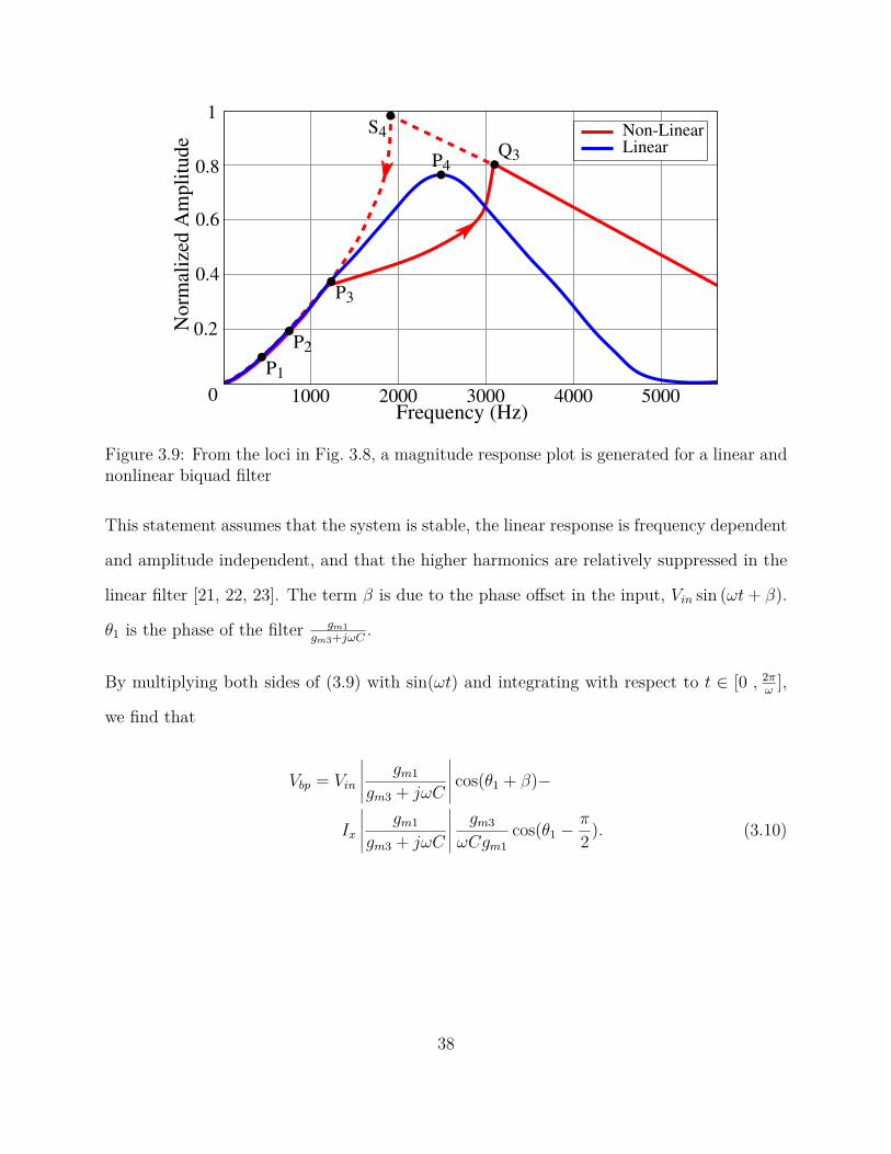
Figure 3.9: From the loci in Fig. 3.8, a magnitude response plot is generated for a linear andnonlinear biquad filter
This statement assumes that the system is stable, the linear response is frequency dependent
and amplitude independent, and that the higher harmonics are relatively suppressed in the
linear filter [21, 22, 23]. The term β is due to the phase offset in the input, Vin sin (ωt + β).
θ1 is the phase of the filter gm1
gm3+jωC.
By multiplying both sides of (3.9) with sin(ωt) and integrating with respect to t ∈ [0 , 2πω
],
we find that
Vbp = Vin
∣
∣
∣
∣
∣
gm1
gm3 + jωC
∣
∣
∣
∣
∣
cos(θ1 + β)−
Ix
∣
∣
∣
∣
∣
gm1
gm3 + jωC
∣
∣
∣
∣
∣
gm3
ωCgm1
cos(θ1 − π
2). (3.10)
38

Similarly, by multiplying both sides of (3.9) with cos(ωt) and integrating, we get
0 = Vin
∣
∣
∣
∣
∣
gm1
gm3 + jωC
∣
∣
∣
∣
∣
sin(θ1 + β)−
Ix
∣
∣
∣
∣
∣
gm1
gm3 + jωC
∣
∣
∣
∣
∣
gm3
ωCgm1
sin(θ1 − π
2). (3.11)
From (3.10) and (3.11), one can eliminate the variable β to simplify the relationship as:
Vbp
Vin
=
∣
∣
∣
∣
∣
gm1
gm3 + sC
∣
∣
∣
∣
∣
(
Ixgm3
Vingm1ωC
)
·
√
√
√
√
(
Vingm1ωC
Ixgm3
)2
− cos2(θ1) − sin(θ1)
. (3.12)
Alternatively, (3.13) can be expressed as:
Vbp
Vin
=
∣
∣
∣
∣
∣
gm1
gm3 + jωC
∣
∣
∣
∣
∣
(
−gm3Ix
ωCgm1Vin
)
cos(θ1 − π
2)+
√
√
√
√1 −(
gm3
ωCgm1
(
Ix
Vin
)
sin(
θ1 − π
2
)
)2
. (3.13)
The nonlinearity of gm2 can be analyzed using the describing function shown in Fig. 2.2,
and is defined as (3.5). Using these approximations, one can express Ix
Vinas
Vbp
VinN(Vbp), which
takes into account the first order approximation of a saturation nonlinearity. More general
methods for analyzing jump criterion of circuits with various types of nonlinearities are
presented by other authors [27, 28, 29, 30].
39

3.3 Architecture of Silicon Implementation
We have designed and prototyped an 11 channel silicon AFE; the architecture and circuit
level schematic of a single channel is shown in Fig 3.10, which consists of a band-pass biquad
filter. A half-wave rectifier, as shown in Fig. 3.10, computes the energy within the frequency
band (determined by the center-frequency and the quality-factor of the biquad filter). The
rectifier is implemented using a pMOS diode which based on the polarity of the biquad
filter output, steers the current towards a pulse-encoder (first-order continuous-time Σ∆
modulator). The output of the rectifier is maintained at a virtual ground by the feedback
amplifier in the pulse-encoder and this reduces the artifacts due to finite output impedance
of the transconductor gm4. The pulse-encoder integrates the rectified current to compute
a measure of the instantaneous energy of the biquad output. It then encodes the energy
signal using pulse-width modulated (PWM) digital spike-trains. The pulses are generated
by comparing the integrator output against a reference voltage Vref which is then used to
turn ON or OFF the reference current Iref that discharges the integrator. It can be shown
that the average of the comparator output tracks the average of the input current, which in
this case is the instantaneous energy of the biquad signal. The transconductance gm1, gm2
and gm3 are tuned by adjusting the bias current of the transcondutors using on-chip current-
mode digital-to-analog converters (shown in Fig. 3.10). The micrograph of the prototyped
silicon AFE is presented in Fig. 3.11a.
All of the transconductors in the biquad are biased in the weak-inversion region, which easily
allows us to observe the jump-resonance phenomenon. In general, transconductors are more
susceptible to nonlinear operation than their switched-capacitor or MOSFET-C counterparts,
which have larger dynamic ranges, and the current-mode biasing can be used to control the
slew-rate of the transconductors. In the mathematical analysis presented in subsection 3.2,
40

Figure 3.10: System and schematic level architecture of one channel in the silicon auditoryfront-end. Transistor-level schematics are shown for: (a) transconductor and (b) operationalamplifier.
the saturating parameter α of the transconductance gm2 was used to introduce non-linearity
into the feed-back architecture and hence introduce jump-resonance in the filter-response.
The parameter δ could be tuned to change the hysteretic behavior. This is a stable and
reliable way of tuning the hysteretic behavior of the filter. However, for the biquad filter
topology used for this work (as shown in Fig. 3.10), modulating δ also affects the value of gm2,
41

(a)
(b)
Figure 3.11: (a) Partial micrograph showing a single channel of the silicon analog front endand (b) the full micrograph of a 27 channel implementation, the first 11 channels are usedfor this AFE.
42

which in-turn affects the center frequency and the Quality factor of the filter. Therefore, for
this paper we resort to modulating the value of |Vbp| to adjust the parameter α. This implies
either adjusting the magnitude of the external stimuli Vin or adjusting the transconductance
gm1 to increase the gain of the filter. Since pushing a filter beyond its slew rate enhances the
jump-resonance (increases the width of the hysteresis and has sharper transitions), one may
also modulate the behavior of jump-resonance through gm1. Therefore, the tuning algorithm
for each AFE channel involved the following steps:
1. Set gm1 to a low-value using the programming DAC such that all transconductors
operate in the linear-region.
2. Adjust gm2 and gm3 (using DACs) such that the frequency response of the AFE channel
has the desired center-frequency and Quality factor. The frequency response of a single
channel is measured by applying a chirp signal (magnitude 100mV) with forward and
reverse frequency sweeps lasting three seconds. The pulse-encoded output produced
by the AFE channel (see Fig. 3.10) is filtered and decimated to obtain the frequency
response during the forward and reverse frequency sweeps.
3. For the fixed value of gm2 and gm3, increase the value of gm1 such that the measured
frequency response exhibits jump-resonance hysteresis with a specific hysteretic width.
Note that the accuracy of the calibration procedure is determined by the accuracy of the
programming DACs. However, the main motivation of this paper is to investigate the effect
of jump-resonance on the performance of a speaker recognition system and future work will
investigate filter topologies that can be used to independently tune the hysteretic behavior.
43

3.4 Measurement Results
Fig. 3.12 shows the measured response obtained from a single channel of the silicon AFE
when the frequency of the input sinusoidal signal is first increased (forward-sweep) and
when the frequency of the input signal is decreased (reverse-sweep). For this result, we have
ensured that all the transconductors operate within the linear range. Therefore, as shown in
Fig. 3.12, the responses of both the forward and reverse sweep match, which is expected from
an linear biquad filter. Table 3.1 summarizes the measured specification of a single-channel
of the fabricated auditory front-end. Note that the filters consume only 3 nW to 30 nW of
power depending on the center-frequency and quality-factor of the biquad.
Figure 3.12: Measured response from the biquad filter when biased in the linear region. Thefrequency of the input signal is swept (i.e. chirp) in the forward (increasing) and reverse(decreasing) direction.
44

Table 3.1: Design and Measured Specification of Fabricated Gm-C Filter
Parameters Value
Technology 0.5 µm CMOS
Supply Voltage 3.3 V
Center-frequency Range 100 Hz – 4 kHz
Input Voltage Range 100 mV
Power Dissipation 3 nW – 30 nW
Capacitance 1.28 pF
Transconductance (design) 0.8 nS – 32 nS
DAC resolution (design) 10 bits
Effective DAC resolution 7 bits
Figure 3.13: Jump resonance obtained when the value of gm1 > gm2.
Figure 3.13 and Figure 3.14 are the jump-resonances observed in the fabricated front-end
for two settings of gm1. Note that the values of the transconductances are adjusted using an
on-chip DAC, so in the measured results we can only report the DAC settings or the relative
values of gm1. For a lower-value of gm1, the width of the hysteresis region reduces and is shown
in Figure 3.13 to be approximately 10Hz. For a larger-value of gm1 the width increases to
50Hz demonstrating that the jump-resonance can be effectively controlled. We have verified
45
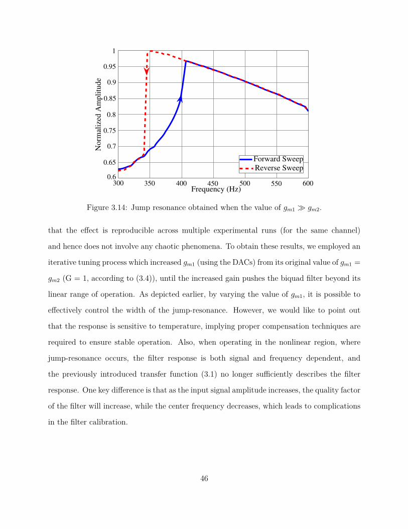
Figure 3.14: Jump resonance obtained when the value of gm1 ≫ gm2.
that the effect is reproducible across multiple experimental runs (for the same channel)
and hence does not involve any chaotic phenomena. To obtain these results, we employed an
iterative tuning process which increased gm1 (using the DACs) from its original value of gm1 =
gm2 (G = 1, according to (3.4)), until the increased gain pushes the biquad filter beyond its
linear range of operation. As depicted earlier, by varying the value of gm1, it is possible to
effectively control the width of the jump-resonance. However, we would like to point out
that the response is sensitive to temperature, implying proper compensation techniques are
required to ensure stable operation. Also, when operating in the nonlinear region, where
jump-resonance occurs, the filter response is both signal and frequency dependent, and
the previously introduced transfer function (3.1) no longer sufficiently describes the filter
response. One key difference is that as the input signal amplitude increases, the quality factor
of the filter will increase, while the center frequency decreases, which leads to complications
in the filter calibration.
46
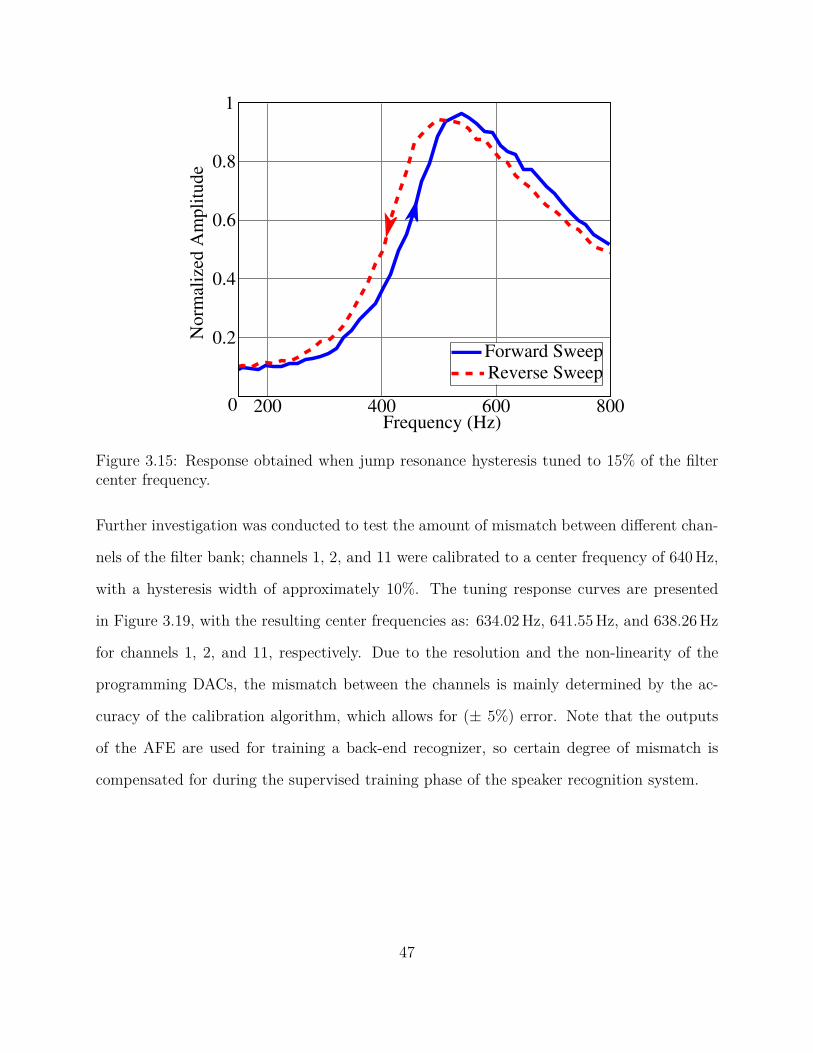
Figure 3.15: Response obtained when jump resonance hysteresis tuned to 15% of the filtercenter frequency.
Further investigation was conducted to test the amount of mismatch between different chan-
nels of the filter bank; channels 1, 2, and 11 were calibrated to a center frequency of 640 Hz,
with a hysteresis width of approximately 10%. The tuning response curves are presented
in Figure 3.19, with the resulting center frequencies as: 634.02 Hz, 641.55 Hz, and 638.26 Hz
for channels 1, 2, and 11, respectively. Due to the resolution and the non-linearity of the
programming DACs, the mismatch between the channels is mainly determined by the ac-
curacy of the calibration algorithm, which allows for (± 5%) error. Note that the outputs
of the AFE are used for training a back-end recognizer, so certain degree of mismatch is
compensated for during the supervised training phase of the speaker recognition system.
47

Figure 3.16: Response obtained when jump resonance hysteresis tuned to 30% of the filtercenter frequency.
3.5 Application to Speaker Recognition
To verify that encoding formant trajectories using jump-resonant hysteresis is beneficial for
recognition, we used the output generated by the fabricated silicon AFE to train a speaker
recognition system. A YOHO speaker verification database, which consists of sets of four
combination lock phrases spoken by 168 speakers, was chosen for training and testing [45, 46].
The experimental set up is shown in Figure 3.20 consisted of a PC based audio system which
was used to play each of the YOHO utterances through an audio interface to the silicon AFE.
The real-time 11 channel pulse-encoded output from the silicon AFE was recorded using an
FPGA and is retrieved back to the PC through a USB interface. The pulse-encoded output
were then post-filtered using a moving average window, after which the output was sub-
sampled at a lower-rate to generate a vector of features specific to the utterance [47].
48

Figure 3.17: Response obtained when jump resonance hysteresis tuned to 60% of the filtercenter frequency.
Figure 3.21 visually compares the output of the AFE with linear-filters and jump-resonance
filters for the utterance “26 · 81 · 57”. To demonstrate that jump-resonance can produce
features that are markedly different from that of a conventional filter-bank based AFE,
we inspect the output of a single filter channel as shown in the Figure 3.22 corresponding
to the same speech utterance “26 · 81 · 57”. The filters of the channel were tuned to a
center frequency of 1.138 kHz. The solid-blue trace is the output of a conventional linear
filter, and the red trace is the output of a jump-resonance filter with a 30% hysteresis. The
dashed-green trace in Figure 3.22 is obtained after scaling and translating the linear-filter
features. While some correlation exists between the two features, the results indicate that
the output of the jump-resonance filters are different. As shown in the top-left portion of
Figure 3.21, between index 10 and 20 of filter channels two and three, the peak responses
are aligned vertically. Observe that the response for the bottom-left portion of Figure 3.21,
corresponding to the jump features, does not have peak responses that are aligned vertically.
49

(a) 435 Hz → 365 Hz → 435 Hz (b) 365 Hz → 435 Hz → 365 Hz
(c) Filter output for Figure 3.18a. (d) Filter output for Figure 3.18b.
Figure 3.18: Measured responses (c) and (d) from the jump-resonance AFE when signalswith different frequency trajectories, shown in (a) and (b) are applied.
Inspecting the original speech signal (in the middle-left of Figure 3.21) between 200 ms and
300 ms at frequencies 200 Hz to 500 Hz, which is roughly the region that would produce the
features previously described, shows that there is a high energy speech pattern that spreads
in frequency. A similar effect is observed between the index points 70–90 in Figure 3.21,
which again shows the local maxima of each filter channel being aligned in time for a linear
filter, while there are shifts in the jump-resonance filter. The region in the original signal that
would have created these features is approximately between 1.3s and 1.4s, which as shown
in Figure 3.21 has a large sweep in frequency content. As theorized earlier, it is possible
50

Figure 3.19: Measured jump-resonance responses for different AFE channels tuned to acommon center frequency and quality factor.
that using the jump-resonance filtering method does lead to additional information about
the frequency trajectory of a signal; it appears that this information is not only apparent
through filter responses that favor speech, as shown in Figure 3.18, but it also manifests as
a phase offset between the multiple filter channels.
In the next set of experiments, the output of the AFE was used to train an SVM based
speaker recognition system, similar tests were done on non-SVM systems [48]. The AFE fil-
ters were calibrated to center frequencies that were spaced according the Mel-scale [35, 49].
For training, 10 speakers (speaker ID: 101-110) were chosen from the YOHO database and
the AFE features were extracted for all utterances corresponding to each speaker. To re-
duce the total number of training points, a K-means clustering was performed (starting
with a random set of initial points) for each speaker to obtain 1000 cluster points for the
51
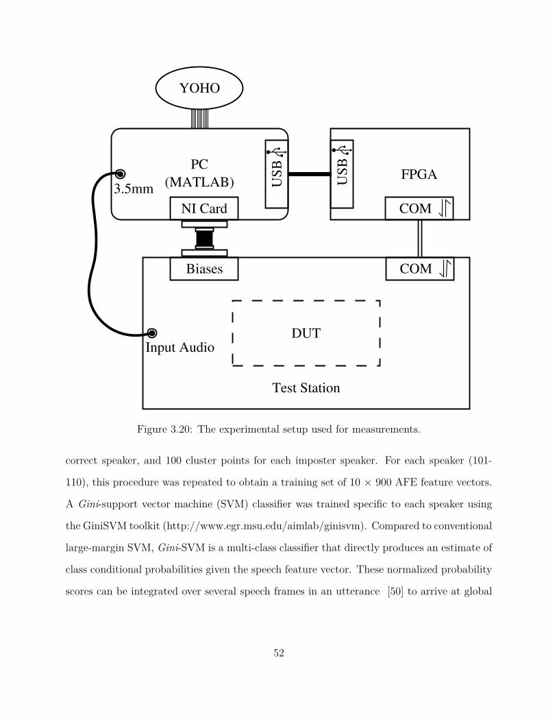
Figure 3.20: The experimental setup used for measurements.
correct speaker, and 100 cluster points for each imposter speaker. For each speaker (101-
110), this procedure was repeated to obtain a training set of 10 × 900 AFE feature vectors.
A Gini-support vector machine (SVM) classifier was trained specific to each speaker using
the GiniSVM toolkit (http://www.egr.msu.edu/aimlab/ginisvm). Compared to conventional
large-margin SVM, Gini-SVM is a multi-class classifier that directly produces an estimate of
class conditional probabilities given the speech feature vector. These normalized probability
scores can be integrated over several speech frames in an utterance [50] to arrive at global
52
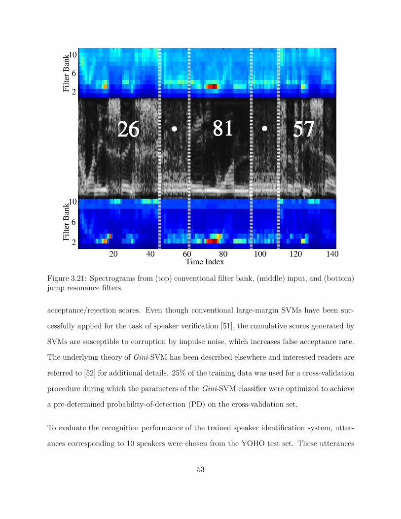
Figure 3.21: Spectrograms from (top) conventional filter bank, (middle) input, and (bottom)jump resonance filters.
acceptance/rejection scores. Even though conventional large-margin SVMs have been suc-
cessfully applied for the task of speaker verification [51], the cumulative scores generated by
SVMs are susceptible to corruption by impulse noise, which increases false acceptance rate.
The underlying theory of Gini-SVM has been described elsewhere and interested readers are
referred to [52] for additional details. 25% of the training data was used for a cross-validation
procedure during which the parameters of the Gini-SVM classifier were optimized to achieve
a pre-determined probability-of-detection (PD) on the cross-validation set.
To evaluate the recognition performance of the trained speaker identification system, utter-
ances corresponding to 10 speakers were chosen from the YOHO test set. These utterances
53
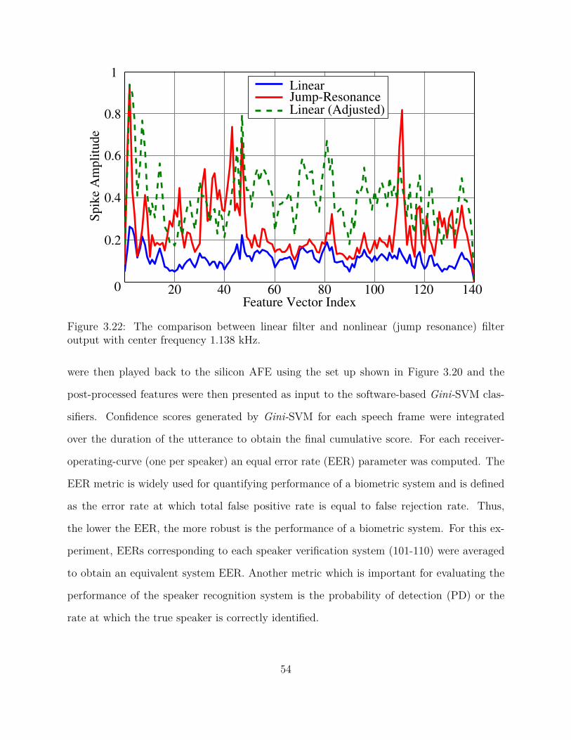
Figure 3.22: The comparison between linear filter and nonlinear (jump resonance) filteroutput with center frequency 1.138 kHz.
were then played back to the silicon AFE using the set up shown in Figure 3.20 and the
post-processed features were then presented as input to the software-based Gini-SVM clas-
sifiers. Confidence scores generated by Gini-SVM for each speech frame were integrated
over the duration of the utterance to obtain the final cumulative score. For each receiver-
operating-curve (one per speaker) an equal error rate (EER) parameter was computed. The
EER metric is widely used for quantifying performance of a biometric system and is defined
as the error rate at which total false positive rate is equal to false rejection rate. Thus,
the lower the EER, the more robust is the performance of a biometric system. For this ex-
periment, EERs corresponding to each speaker verification system (101-110) were averaged
to obtain an equivalent system EER. Another metric which is important for evaluating the
performance of the speaker recognition system is the probability of detection (PD) or the
rate at which the true speaker is correctly identified.
54

Table 3.2 summarizes the EER and PD of the speaker identification system corresponding
to different durations of the moving average window and window step-size. The table com-
pares the recognition metrics obtained using the jump-resonance based AFE, the recognition
metrics obtained using the linear-filter AFE and the recognition metrics obtained using a
MFCC-based AFE implemented in software. To ensure a fair comparison between the dif-
ferent features, the recognition results have been reported for a system using 11-dimensional
MFCC features and using 22-dimensional MFCC features (which includes 11 velocity or ∆
coefficients). The recognition results show that the jump-resonance based AFE demonstrates
better performance than the linear filter-bank based AFE and under some conditions even
outperforms its MFCC counterpart.
The linear filter setup achieved the best performance for a step size of 12 ms and a window
size of 16 ms, resulting in a probability of detection (PD) of 95.63% and an equal error
rate (EER) of 2.01%, as outlined in Table 3.2. The jump features (Jumpb) were able to
outperform the linear hardware features with a PD of 100% for all step sizes, and achieved
a minimal EER of 0.14% when the overlap was 0 ms. For this jump configuration, the
hardware features were able to outperform the simulated Mel-frequency cepstral coefficients
(MFCC) with no additive noise, which had a minimum EER of 2.01% and corresponding PD
of 98.75%. In fact, the performance is at par with the 22-dimensional MFCC features. This
attribute verifies our hypothesis that jump-resonance based features can encode information
corresponding to ∆ features which are difficult to compute in analog AFEs. We would like to
point out that jump-resonance with smaller hysteresis widths (Jumpa) yielded results that
were worse compared to that of the linear features, with a maximum PD of 95.63% and EER
of 2.88%.
The results presented in Table 3.3 are from testing with speaker IDs 101-110 and 201-210,
for a total of 20 speakers. In this case, the linear filter was only able to achieve a 90.94%
55
PD maximum, and 5.39% EER minimum for step sizes of 8 ms and 12 ms, respectively. The
jump features (Jumpb) also had a deterioration in performance with a maximum PD of
98.75% for an 8 ms step size and a minimum EER of 1.50% for step sizes 12ms and 16ms
respectively. Both features suffered an increase of the EER in excess of 1%, however, the
smaller jump features’ (Jumpa) minimum EER only rose by 0.29%. It’s maximum PD also
increased to 95.94%, instead of decreasing, which suggests that for speakers 201-210 the
optimal jump width may be closer to 15% of the center frequency compared to the 30% used
in Jumpb. Although the Jumpb features may not have the optimal parameters, it is still able
to outperform the traditional linear features and the software MFCC (11-dimension) speaker
recognition results for the 20 speakers tested. The experimental results show that it may be
possible to improve the performance of speaker detection algorithms by carefully optimizing
the hysteretic properties of jump-resonance [53]. Additional studies have demonstrated the
potential for using jump-resonance in filtering of electromyography to extract speech induced
muscle activity of individuals [54, 55, 56, 57].
56

Tab
le3.
2:C
ompar
ison
ofE
ER
and
PD
obta
ined
usi
ng
an11
filt
erA
FE
for
alinea
ran
dju
mp
reso
nan
cefilt
erban
kw
ith
anM
FC
C-b
ased
syst
em
Ex
peri
men
tal
sett
ing
s:w
ind
ow
size
=1
6m
s,n
um
ber
of
speak
ers
=1
0
Lin
ear
Jum
pa
[Fig
ure
3.15
]Jum
pb
[Fig
ure
3.16
]M
FC
C(1
1filt
ers)
MF
CC
(22
filt
ers)
Ste
pS
ize
EE
RP
DE
ER
PD
EE
RP
DE
ER
PD
EE
RP
D4m
s0.
0288
0.95
630.
0441
0.93
130.
0063
1.00
000.
0187
0.98
120.
0035
1.00
008m
s0.
0253
0.95
630.
0431
0.92
500.
0104
1.00
000.
0247
0.96
880.
0017
1.00
0012
ms
0.0
20
10
.95
63
0.03
400.
9437
0.00
661.
0000
0.02
010.
9875
0.00
760.
9938
16m
s0.
0260
0.93
750.
0288
0.95
630
.00
14
1.0
00
00.
0201
0.96
880.
0017
1.00
00
Tab
le3.
3:C
ompar
ison
ofE
ER
and
PD
obta
ined
usi
ng
an11
filt
erA
FE
for
alinea
ran
dju
mp
reso
nan
cefilt
erban
kw
ith
anM
FC
C-b
ased
syst
em
Ex
peri
men
tal
sett
ing
s:w
ind
ow
size
=1
6m
s,n
um
ber
of
speak
ers
=2
0
Lin
ear
Jum
pa
[Fig
ure
3.15
]*Jum
pb
[Fig
ure
3.16
]M
FC
C(1
1filt
ers)
MF
CC
(22
filt
ers)
Ste
pS
ize
EE
RP
DE
ER
PD
EE
RP
DE
ER
PD
EE
RP
D4m
s0.
0576
0.88
750.
0376
0.95
000.
0166
0.97
810.
0213
0.98
120.
0040
1.00
008m
s0.
0569
0.9
09
40.
0360
0.94
060.
0163
0.9
87
50.
0247
0.97
810.
0043
1.00
0012
ms
0.0
53
90.
9031
0.03
410.
9594
0.0
15
00.
9781
0.02
160.
9812
0.00
891.
0000
16m
s0.
0586
0.88
120.
0317
0.95
940
.01
50
0.97
190.
0260
0.97
500.
0079
0.99
69
57

Chapter 4
Linearized Floating-Gate Injection
With respect to portable or embedded sensors, one of the biggest design considerations is
energy. Can we harvest the required energy from the deployed environment? Does the
sensor require a battery or other energy storage solution? How long can we expect sensor
to function on a given amount of energy? Under such stringent power constraints, we aim
to eliminate the overhead and losses from power regulators, data converters, digital signal
processors and conventional memory structures. In this section, a method for data-logging
that is powered by the input stimuli itself will be detailed.
4.1 Floating-Gate Implementation
4.1.1 Principle of Operation
In pursuit of realizing a “sense-now, analyze-later” sensor, the Adaptive Integrated Mi-
crosystems Laboratory has been studying the floating-gate (FG) transistor. Floating-gate
transistors are a nonvolatile programmable circuit that has been used in digital EEPROM
and flash memory applications [58]. The FG transistor is a metal oxide semiconductor field
effect transistor (MOSFET) with a polysilicon gate that is DC-insulated by a surrounding
58

layer of silicon dioxide. Since the gate is surrounded by a good electrical insulator, any charge
that is on the gate will, with high probability, remain there. Taking advantage of the lossless
property of a FG MOSFET, structures can be designed to use lossless charge sharing to
improve input range, lower circuit complexity, and build independently and simultaneously
trimmable circuits [59, 60].
(a)
Floating Gate (Al)
SiO2
tox
Drain (Si)
e-
MechanicalExcitation
3.2 eV
EC
EV
Hot e-
PZT
(b)
Figure 4.1: Impact ionized hot-electron injection illustrations (a) energy band diagram and(b) a cross-sectional view of P-MOSFET FG transistor.
A common method for programming FG transistors is through Fowler-Nordheim (FN) tun-
neling and impact ionized hot-electron injection (IIHEI) [61, 62]. IIHEI for a p-channel
MOSFET is induced with the introduction of a strong electric field being formed between
59

the drain-to-channel depletion region. When subjected to a strong electric field, the pri-
mary carriers in a p-channel, the holes, can gain sufficient energy to dislodge electrons via
impact ionization with high probability, see Figure 4.1 for an energy band diagram and cross-
sectional view to aid in the illustration of this process. In this illustration, the strong electric
field is supplied by an external piezoelectric transducer. Any electron that has been dislodged
is a “hot electron” that can accelerate towards the channel region, gaining kinetic energy in
the process. If the total kinetic energy exceeds 3.2 eV, the momentum of the electron can be
sufficient to overcome the Si-SiO2 barrier, thus allowing the hot electron to get injected into
the oxide. For the 0.5 µm CMOS process available through the MOSIS educational program,
IIHEI will require a voltage of approximately 4.2 V to generate a sufficient electric field to
add electrons onto the FG (and thus reducing the voltage potential). To remove electrons
from the FG the FN tunneling process is used, whereby a high voltage potential (>14 V in
the 0.5 µm process) is applied across a parasitic capacitor that is coupled to the FG. This
will draw away any charge on the FG and leave it in an empty state.
Because FN tunneling requires high voltages, it is treated as a global erasure mechanism for
the FG memory, and IIHEI is used for programming specific analog memory values. IIHEI
current Iinj, in a p-channel MOSFET, has been shown to be dependent on the transistor
source current Is, the source-to-drain voltage Vsd, and the gate-to-drain voltage Vgd across
the transistor. To date, this dependence has only been described using empirical models,
such as this one:
Iinj = αIS exp
(
λVsd
Vinj
)
exp
[
−β
(Vgd + δ)2
]
, (4.1)
which is assumed to be valid for most of the transistor’s operating region (weak, moderate,
and strong inversion). The parameters α, λ, β, δ, and Vinj are estimated from measured data.
With a circuit architecture as in Figure 4.2, all other factors that affect the injection current
(IS, Vsd, and Vgd) are held at constant potentials, thus the injection current Iinj as modeled
60

VFG
ChN
VTun
MFG
V'FG
VRef
Injen
SN
VP2
VP1
External
Piezo
ChN
CFG
Figure 4.2: The core of the PFG’s linear injector core has many configuration states, thetransistor-level details are shown here.
in (4.1) is also constant.
MFG
V'FG
VRef
Piezo
CFG
V'Ref
Figure 4.3: Equivalent circuity when configured for self-powered operation, with Vdd sup-plied by the input stimuli on the piezo through Figure 4.9.
61

During the sensing mode (Figure 4.3), the switch Sp is open, thus enabling the negative
feedback of the operational amplifier to be formed in conjunction with the FG. With a
constant Iref , the source-to-gate voltage, Vsg will be kept constant during injection. The
operational amplifier will continuously adjust the control-gate voltage Vcg to maintain a
constant source-to-drain voltage Vsd, thereby ensuring a constant injection current. For
reading out the stored value, the switch is closed (Figure 4.4c), connecting the control-gate
to a ground reference, thus the floating-gate voltage Vfg is a function of the previously injected
charge and the capacitor Cfg. Omitting the mathematical derivation, the injection current
during sensing was shown to be:
Iinj = I0inj exp
[
− (Gs + Gfg) t
CT (1 + AV)
]
. (4.2)
Where Gs and Gfg are the injection transconductance parameters with respect to the source
and floating-gate terminals, and can be estimated to be in the range 0.149 to 2.316 fS
for reference currents between 45 and 90 nA. AV is the gain of the operational amplifier,
which only requires a small-signal gain of 40 dB. t is the injection time and CT is the
total capacitance at the floating-gate, including the parasitic and nonparasitic floating-gate,
tunneling, source, drain, and bulk capacitors. Additional literature detailing applications of
the FN tunneling and IIHEI process, including a method for recording the time-of-occurrence
of injection are available [63, 64, 65, 66, 67, 68]. Many of these methods are dependent on a
novel self-powered timer devices that was developed in the Adaptive Integrated Microsystems
laboratory [69, 70].
4.1.2 Circuit Implementation
Taking the linear injector designed for self-powered sensing using piezoelectric transducers,
as detailed in Section 4.1.1, a System-on-Chip (SoC) is designed following the block diagram
62
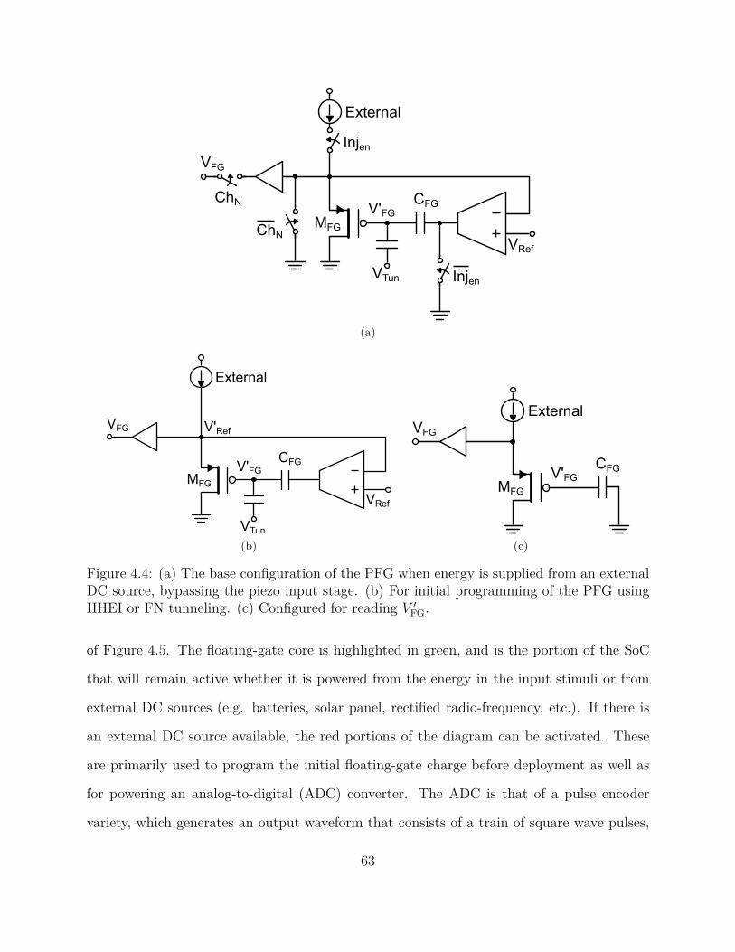
VFG
ChN
VTun
MFG
V'FG
VRef
Injen
External
ChN
CFG
Injen
(a)
VFG
VTun
MFG
V'FG
VRef
External
CFG
V'Ref
(b)
VFG
MFG
V'FG
External
CFG
(c)
Figure 4.4: (a) The base configuration of the PFG when energy is supplied from an externalDC source, bypassing the piezo input stage. (b) For initial programming of the PFG usingIIHEI or FN tunneling. (c) Configured for reading V ′
FG.
of Figure 4.5. The floating-gate core is highlighted in green, and is the portion of the SoC
that will remain active whether it is powered from the energy in the input stimuli or from
external DC sources (e.g. batteries, solar panel, rectified radio-frequency, etc.). If there is
an external DC source available, the red portions of the diagram can be activated. These
are primarily used to program the initial floating-gate charge before deployment as well as
for powering an analog-to-digital (ADC) converter. The ADC is that of a pulse encoder
variety, which generates an output waveform that consists of a train of square wave pulses,
63
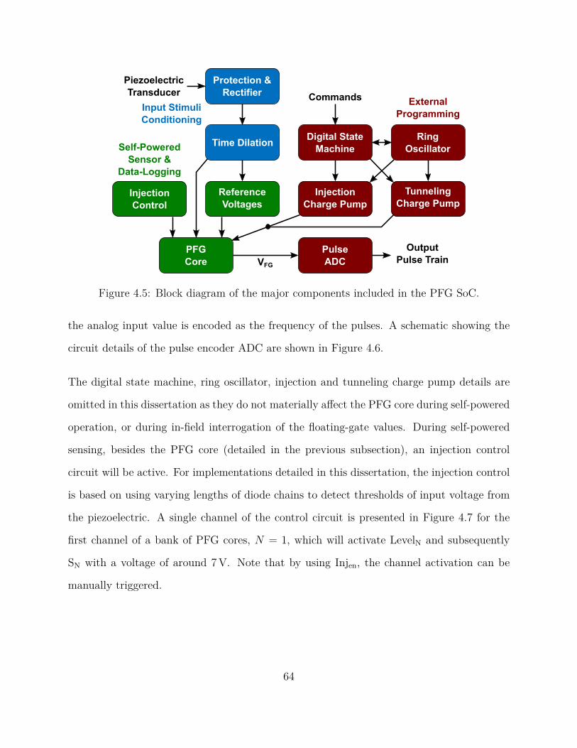
Protection &
Rectifier
Time Dilation
Reference
VoltagesInjection
Control
PFG
Core
Pulse
ADC
Injection
Charge Pump
Tunneling
Charge Pump
Digital State
Machine
Ring
Oscillator
Piezoelectric
Transducer
Output
Pulse TrainVFG
CommandsInput Stimuli
Conditioning
Self-Powered
Sensor &
Data-Logging
External
Programming
Figure 4.5: Block diagram of the major components included in the PFG SoC.
the analog input value is encoded as the frequency of the pulses. A schematic showing the
circuit details of the pulse encoder ADC are shown in Figure 4.6.
The digital state machine, ring oscillator, injection and tunneling charge pump details are
omitted in this dissertation as they do not materially affect the PFG core during self-powered
operation, or during in-field interrogation of the floating-gate values. During self-powered
sensing, besides the PFG core (detailed in the previous subsection), an injection control
circuit will be active. For implementations detailed in this dissertation, the injection control
is based on using varying lengths of diode chains to detect thresholds of input voltage from
the piezoelectric. A single channel of the control circuit is presented in Figure 4.7 for the
first channel of a bank of PFG cores, N = 1, which will activate LevelN and subsequently
SN with a voltage of around 7 V. Note that by using Injen, the channel activation can be
manually triggered.
64

VN1
VN2
VP2
VP1
Vin
Digout
Figure 4.6: The analog-to-digital (ADC) circuit is implemented using a pulse encoder. Thefrequency of the output train correlates to the input analog value.
In the self-powered mode of Figure 4.5, the last key components are the voltage references.
There are multiple voltage references built into the chip, and they mostly follow the archi-
tecture of Figure 4.8. It consists of cascaded current mirrors that are variably tunable by
adding external resistances to Rdec or Rinc. Most references have been designed with an on
board resistor such that keeping Rdec floating and Rinc tied to ground will set the PMOS
and NMOS voltage biases to their desired points. The two capacitors and NMOS transistors
on the left-hand side of the circuit operate as a startup circuit to ensure that the current
mirrors are in a valid operating region.
The blue regions of the Figure 4.5 denote circuitry that is used as for input stimuli condition-
ing. For the purposes of this dissertation the input stimuli is typically assumed to be that
65

Vp1
LevelN
x 9+N
Vp2
Injen
SN
Figure 4.7: During self-powered mode, the injection is controlled by diode threshold detec-tion, each channel (N) will have a varying activation threshold.
of a piezoelectric transducer generating voltages between 7 V and 12 V. Since many desired
target applications tend to generate voltages larger than that range, we utilize a time-dilation
circuit and overvoltage protection diodes as shown in Figure 4.9 [71, 72, 73, 74]. The left
portion of the figure is an equivalent model of a piezoelectric transducer. As the figure
illustrates, the input conditioning consists of a parallel capacitor to filter some high fre-
quency content and smooth out minor ripples, series resistors to limit inrush current, diode
chains that will short the piezoelectric when exceedingly large voltages are present, and a
full bridge rectifier to generate the on-chip supply rails. The portion of the figure on the
right, highlighted in purple, is the time-dilation circuitry.
For the sake of completeness, the transistor-level schematics for some of the components
presented in previous figures are included here. Namely: the comparator (Figure 4.10),
which is used in the pulse encoder ADC; the transconductance amplifier (Figure 4.11) that
comprises the feedback amplifier of the PFG core; and an operational amplifier (Figure 4.12)
66

VN1
VN2
VP2
VP1
Rinc
Rdec
Figure 4.8: Schematic showing the transistor-level implementation for voltage references.This circuit is implemented multiple times to generate the necessary onboard voltages, andcan be tuned via external resistance.
......
...
Vdd
CTD
Stimuli
Figure 4.9: On the left a piezoelectric transducer is modeled. The center portion includesseries resistance to limit inrush current, diode chains to prevent overvoltage, and a full bridgerectifier. The output of the full bridge rectifier is attached to a time-dilation componentbefore serving the chip as Vdd.
67

VN1
Vneg
Vpos
Vout
Figure 4.10: The transistor-level implementation of the comparator used in the pulse encoderADC.
that is used whenever an analog signal needs buffering before being sent off-chip. The
operational amplifier also serves as an isolation buffer between multiple PFG channels and
the single ADC that is on-board. Note that the transconductance amplifier has been designed
and biased to operate in a current-starved sub-threshold region, thus shorting its output to
ground will not result in significant damage.
This circuit architecture has been reported first by [75, 76] as having a linearity greater than
13-bits, with other circuit parameters listed in Table 4.1 [77]. The same circuit architec-
ture, or sensor core, has been integrated with piezoelectric sensing and successfully deployed
in numerous field applications, including those that operate within RF energy harvesting
power envelopes [78, 79, 80, 81]. Details of some of the deployments undertaken as part
of this dissertation research follows in Chapter 6, with additional applications reported in
the Appendices. A micrograph showing one implementation of a fabricated linear injector
System-on-Chip (SoC) is presented as Figure 4.13.
68

V+ V-
Iout
CL
Vb
Figure 4.11: This transconductance amplifier is current-starved and utilized as the feedbackamplifier of the PFG core.
V+ V-
Vout
CM
Vb
Figure 4.12: When buffering analog signals before connecting to the pads of the chip, thisop-amp is used.
69

Charge Pumps
Clock Generator
PF
G C
ore
Bias &DigitalControl
TimeDilation
OutputStage
Figure 4.13: Micrograph of an integrated solution with floating-gate linear injector core andnecessary supporting circuitry. The die is 1.5 × 1.5 mm2, and fabricated through MOSIS.
4.2 Laboratory Characterization Results
4.2.1 Linearity
Starting with an “empty”, or fully tunneled floating-gate, we apply a one second injection
pulse from a function generator and record the stored floating-gate voltage after each injec-
tion. Supply voltage to the chip was 1.8 V and the injector’s reference voltage was 5 V. The70
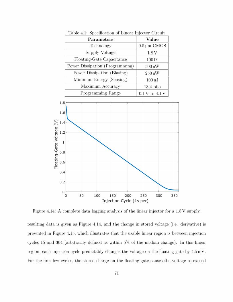
Table 4.1: Specification of Linear Injector Circuit
Parameters Value
Technology 0.5 µm CMOS
Supply Voltage 1.8 V
Floating-Gate Capacitance 100 fF
Power Dissipation (Programming) 500 nW
Power Dissipation (Biasing) 250 nW
Minimum Energy (Sensing) 100 nJ
Maximum Accuracy 13.4 bits
Programming Range 0.1 V to 4.1 V
0 50 100 150 200 250 300 350
Injection Cycle (1s per)
0
0.2
0.4
0.6
0.8
1
1.2
1.4
1.6
1.8
Flo
ating-G
ate
Voltage (
V)
Figure 4.14: A complete data logging analysis of the linear injector for a 1.8 V supply.
resulting data is given as Figure 4.14, and the change in stored voltage (i.e. derivative) is
presented in Figure 4.15, which illustrates that the usable linear region is between injection
cycles 15 and 304 (arbitrarily defined as within 5% of the median change). In this linear
region, each injection cycle predictably changes the voltage on the floating-gate by 4.5 mV.
For the first few cycles, the stored charge on the floating-gate causes the voltage to exceed
71

0 50 100 150 200 250 300 350
Injection Cycle (1s per)
-10-1
-10-2
-10-3
-10-4
Flo
atin
g-G
ate
Vo
lta
ge
Δ (
V)
4.5 mVAverage Δ
Figure 4.15: Plot showing the change in floating-gate voltage per injection cycle of Fig-ure 4.14.
the maximum output swing of the on-chip buffer and similarly near the tail end of the lin-
ear region the buffer has trouble faithfully tracking the change as it is not designed to be
rail-to-rail.
From the data of the linear region in Figure 4.14, an analysis into the Integral Nonlinearity
(INL) and Differential Nonlinearity (DNL) are calculated and shown as Figure 4.16. The
resulting effective number of bits, 12.9, compares favorably to the earlier published results
considering this version of the chip has been compacted to a 1.5 × 1.5 mm2 die on a QFN
package and includes supporting circuitry such as: charge pumps, digital state machines,
multiple channels, buffers, and an analog-to-digital converter. A slight decrease from the
reported 13.5 bits can also be attributed to the lower supply voltage utilized (1.8 V versus
4 V), which exacerbates the impact of having non-ideal buffers. Other researchers have
reported data retention of over eight years for at least eight bits of precision [82].
72
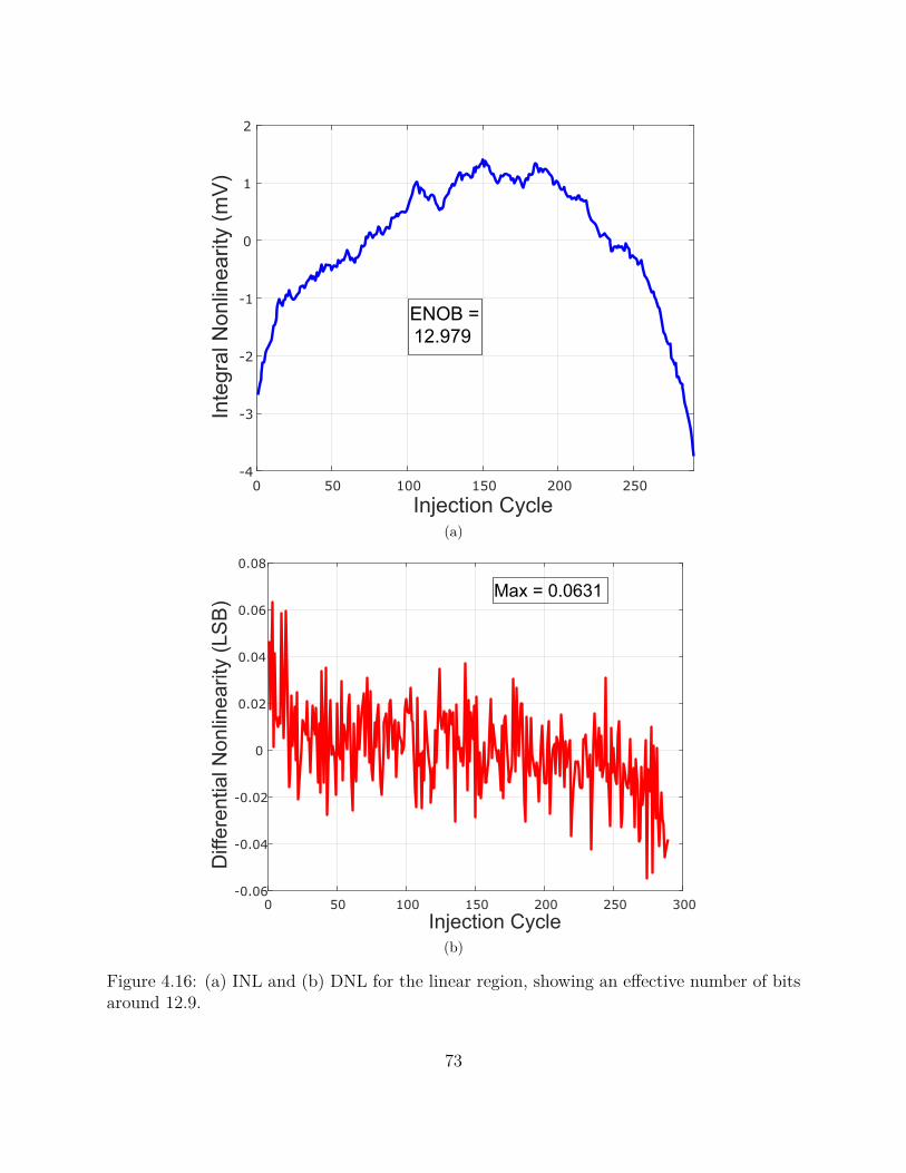
0 50 100 150 200 250
Injection Cycle
-4
-3
-2
-1
0
1
2
Inte
gra
l N
on
line
arity
(m
V)
ENOB =
12.979
(a)
0 50 100 150 200 250 300
Injection Cycle
-0.06
-0.04
-0.02
0
0.02
0.04
0.06
0.08
Diffe
ren
tia
l N
on
line
arity
(L
SB
)
Max = 0.0631
(b)
Figure 4.16: (a) INL and (b) DNL for the linear region, showing an effective number of bitsaround 12.9.
73
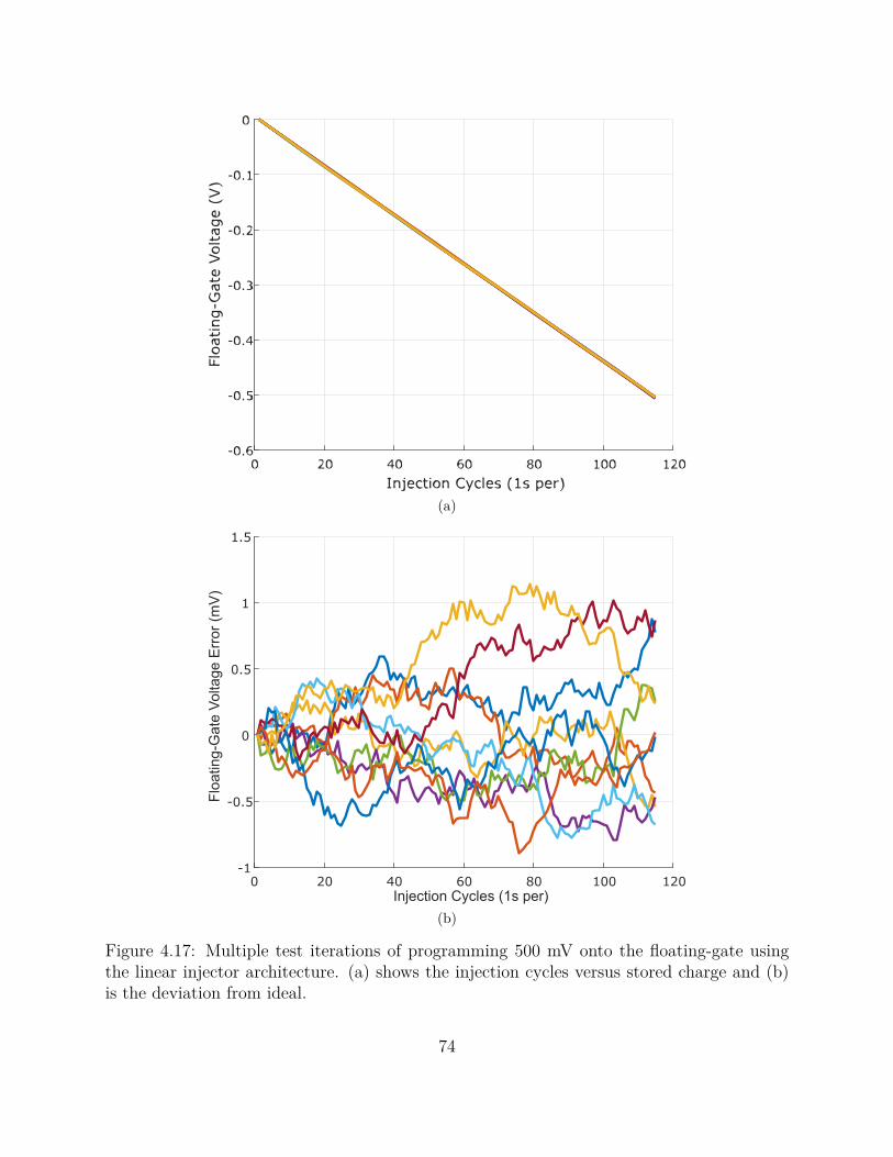
(a)
0 20 40 60 80 100 120
Injection Cycles (1s per)
-1
-0.5
0
0.5
1
1.5
Flo
atin
g-G
ate
Vo
lta
ge
Err
or
(mV
)
(b)
Figure 4.17: Multiple test iterations of programming 500 mV onto the floating-gate usingthe linear injector architecture. (a) shows the injection cycles versus stored charge and (b)is the deviation from ideal.
74

4.2.2 Repeatability and Stability
A floating-gate was initially tunneled to the linear region, and repeatedly injected over 100
cycles with a reference voltage of 5 V and supply voltage of 1.8 V. The result of running
this test for 10 runs is plotted as Figure 4.17a, and the deviation from ideally linear is given
in Figure 4.17b. This testing shows that across a large range of the floating-gate, and over
multiple iterations, the expected systematic error is below 0.1 percent. The main cause of
the error is the non-ideal voltage references implemented within the SoC, as even in a stable
thermal environment small deviations and drift can be observed as in Figure 4.18.
Figure 4.18: The on-board reference voltage is not ideal and exhibits some deviation even ina temperature-stable environment.
The sensitivity, or precision, of how much charge is “recorded” onto the floating gate per in-
jection cycle is tunable via an external resistor to the onboard voltage references. Figure 4.19
shows the variability in sensitivity using reference voltages from 4.5 V to 5.3 V, 4.19a presents
75

0 1000 2000 3000 4000 5000 6000 7000 8000 9000
Injection Cycles (1s per)
-1.4
-1.2
-1
-0.8
-0.6
-0.4
-0.2
0
Flo
ating-G
ate
Voltage C
hange (
V)
4.50
4.60
4.70
4.80
4.90
5.00
5.10
5.20
5.30
Reference (V)
(a)
100 101 102 103 104
Injection Cycles (1s per)
-1.4
-1.2
-1
-0.8
-0.6
-0.4
-0.2
0
Flo
ating-G
ate
Voltage C
hange (
V)
4.50
4.60
4.70
4.80
4.90
5.00
5.10
5.20
5.30
Reference (V)
(b)
Figure 4.19: Varying the reference voltage allows tuning of the sensitivity of the precision,x-axis in (a) linear and (b) logarithmic scale.
76

the data with a linear scale for the x-axis to reinforce that the data logging is linear while
4.19b is plotted on a logarithmic x-axis to give some insight into how a linear change in refer-
ence voltage gives rise to a logarithmic relation for maximum number of recordable injection
cycles. It should be noted that with a sufficiently large reference voltage, the system would
act equivalently to a single level cell NAND flash memory in that the stored value is binary.
On the other hand, as discussed earlier, the minimum voltage for reliable injection in this
process is approximately 4.2 V — with a reference voltage near this threshold the maximum
number of stored cycles would be exponentially larger. However, our earlier analysis leads
us to assume a maximum usable linearity of about 12 to 13 bits, which would be just under
8,192 unique points. Hence, the minimum reference voltage we show in Figure 4.19 is 4.5 V,
which already exceeds that number in this particular test configuration.
4 4.2 4.4 4.6 4.8 5 5.2 5.4 5.6 5.8 6
Reference Voltage (V)
10-5
10-4
10-3
10-2
10-1
100
Inje
ction p
er
1 s
(V)
Figure 4.20: A linear change in reference voltage leads to an exponential change in theamount of charge injected per cycle.
77
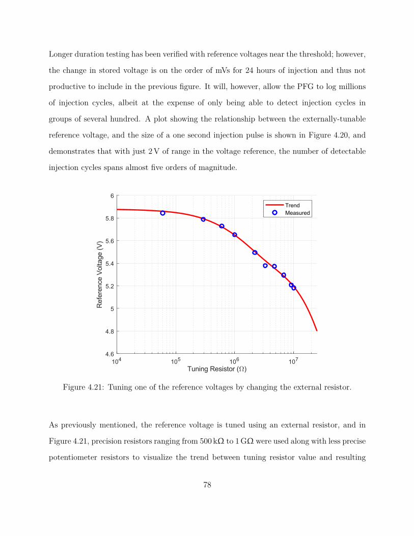
Longer duration testing has been verified with reference voltages near the threshold; however,
the change in stored voltage is on the order of mVs for 24 hours of injection and thus not
productive to include in the previous figure. It will, however, allow the PFG to log millions
of injection cycles, albeit at the expense of only being able to detect injection cycles in
groups of several hundred. A plot showing the relationship between the externally-tunable
reference voltage, and the size of a one second injection pulse is shown in Figure 4.20, and
demonstrates that with just 2 V of range in the voltage reference, the number of detectable
injection cycles spans almost five orders of magnitude.
Figure 4.21: Tuning one of the reference voltages by changing the external resistor.
As previously mentioned, the reference voltage is tuned using an external resistor, and in
Figure 4.21, precision resistors ranging from 500 kΩ to 1 GΩ were used along with less precise
potentiometer resistors to visualize the trend between tuning resistor value and resulting
78
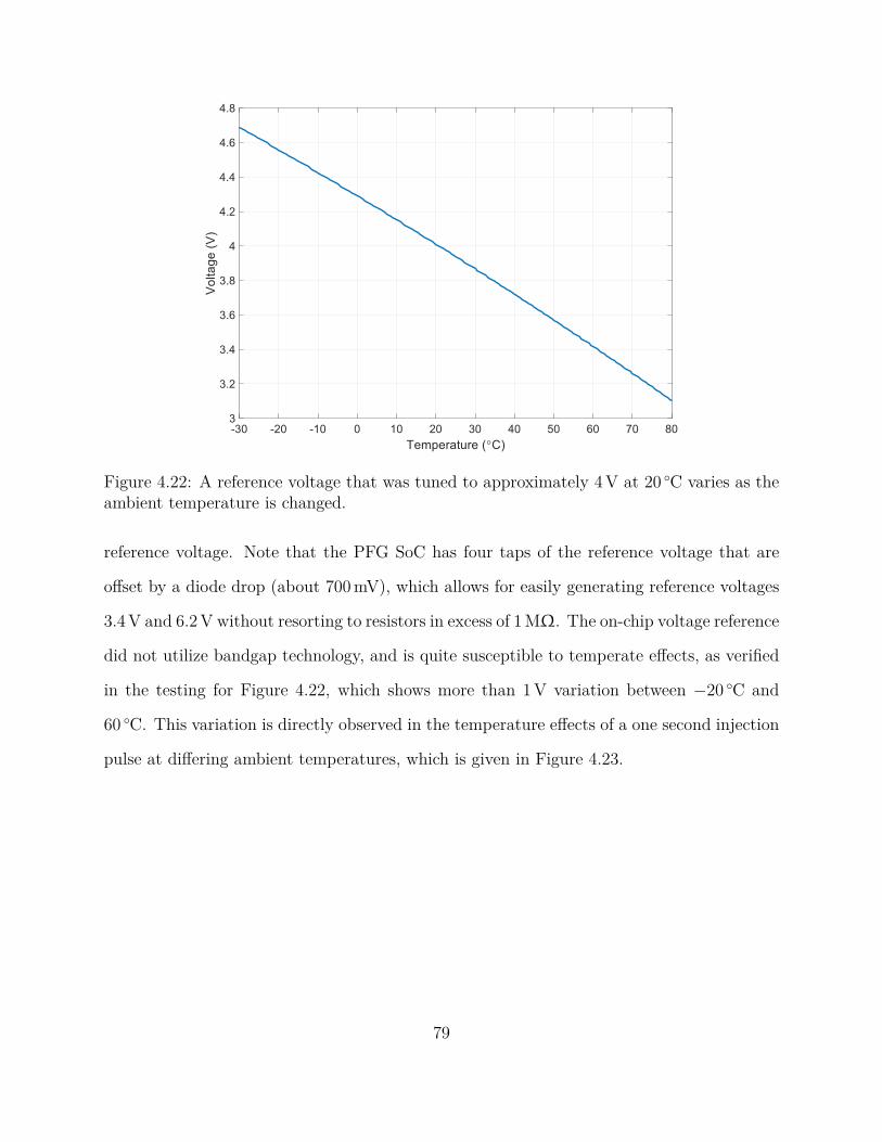
Figure 4.22: A reference voltage that was tuned to approximately 4 V at 20 C varies as theambient temperature is changed.
reference voltage. Note that the PFG SoC has four taps of the reference voltage that are
offset by a diode drop (about 700 mV), which allows for easily generating reference voltages
3.4 V and 6.2 V without resorting to resistors in excess of 1 MΩ. The on-chip voltage reference
did not utilize bandgap technology, and is quite susceptible to temperate effects, as verified
in the testing for Figure 4.22, which shows more than 1 V variation between −20 C and
60 C. This variation is directly observed in the temperature effects of a one second injection
pulse at differing ambient temperatures, which is given in Figure 4.23.
79
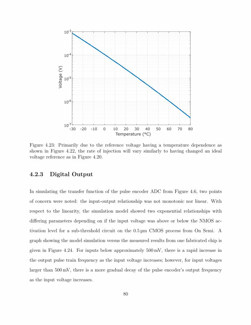
-30 -20 -10 0 10 20 30 40 50 60 70 80
Temperature (°C)
10-7
10-6
10-5
10-4
10-3
Voltage (
V)
Figure 4.23: Primarily due to the reference voltage having a temperature dependence asshown in Figure 4.22, the rate of injection will vary similarly to having changed an idealvoltage reference as in Figure 4.20.
4.2.3 Digital Output
In simulating the transfer function of the pulse encoder ADC from Figure 4.6, two points
of concern were noted: the input-output relationship was not monotonic nor linear. With
respect to the linearity, the simulation model showed two exponential relationships with
differing parameters depending on if the input voltage was above or below the NMOS ac-
tivation level for a sub-threshold circuit on the 0.5 µm CMOS process from On Semi. A
graph showing the model simulation versus the measured results from one fabricated chip is
given in Figure 4.24. For inputs below approximately 500 mV, there is a rapid increase in
the output pulse train frequency as the input voltage increases; however, for input voltages
larger than 500 mV, there is a more gradual decay of the pulse encoder’s output frequency
as the input voltage increases.
80

0 0.2 0.4 0.6 0.8 1 1.2 1.4 1.6 1.8
ADC Input, Buffered VFG
(V)
0
500
1000
1500
2000
2500
3000
3500
4000
4500
AD
C O
utp
ut,
Puls
e T
rain
Fre
quency (
Hz)
Model
Measured
Figure 4.24: The PFG SoC has a pulse encoder analog-to-digital output stage, with a non-monotonic relation between floating-gate voltage and output pulse train frequency.
0
1000
2000
3000
4000
5000
Outp
ut F
requency (
Hz)
0 0.2 0.4 0.6 0.8 1 1.2 1.4 1.6 1.8
Floating-Gate Voltage (V)
0
20
40
60
80
100
Duty
Cycle
(%
) Inflection at
V = 0.47
Figure 4.25: Although the frequency output of the pulse encoder is not monotonic, as demon-strated in Figure 4.24, the duty cycle of the output pulse train allows one to differentiatebetween same output frequencies.
81

The issue of having a non-linear transfer function was not a large concern for the prototype
SoC. Since the measured response closely matched the model, a simple lookup table could
translate the measured output frequency to its equivalent input voltage. The non-monotonic
nature is also not of concern since one can discern whether or not the measured output
frequency correlates to an input voltage that is above or below the inflection point. This is
illustrated int the average measured results for five chips as shown in Figure 4.25. For larger
input voltages, the pulse encoder maintains a very low duty cycle (around 3 to 5%). With
smaller input voltages, the duty cycle will rapidly tend towards 100%.
0 0.2 0.4 0.6 0.8 1 1.2 1.4 1.6 1.8
Floating-Gate Voltage (V)
102
103
104
Outp
ut F
requency (
Hz)
-10°C 0
°C 10
°C 20
°C 30
°C 40
°C
Figure 4.26: The ADC’s charge rate is a function of the onboard reference voltages, andsuffers from temperature effects.
Another limitation of the implemented pulse encoder is that the biasing voltages depend
on the voltage reference of Figure 4.8. Because the 0.5 µm On Semi CMOS process did
not have readily available bipolar transistors or other components for creating a bandgap
or other high performance voltage reference. The Proportional To Absolute Temperature
82

-30 -20 -10 0 10 20 30 40 50 60 70 80
Temperature ( °C)
0.0
0.2
0.4
0.6
0.8
1.0
Corr
ective F
acto
r
Figure 4.27: The necessary corrective scaling to apply to measurements taken at typicaltemperatures.
(PTAT) current source generated by the resistor (any combination of internal or external)
of Figure 4.8 has a strong temperature dependence that causes the output bias voltages
to change rather noticeably. In Figure 4.26, a fabricated PFG chip was tunneled to 1.8 V
equivalent charge, and placed in a thermally controlled environment chamber. It was then
injected in 1 s intervals with a reference voltage of 4.8 V, which decreased the floating-gate
voltage until the pulse encoder output’s duty cycle increased to 100%. The general trend that
was simulated in Figure 4.24 remains in tact across the tested temperatures, and the general
trend shows that higher ambient temperatures result in higher output pulse train frequencies.
Also, the inflection point does not change significantly due to changes in temperature. This
test procedure was repeated for a litany of temperatures to generate the corrective factor
of Figure 4.27. To apply the corrective factor, the measured PFG pulse encoder output
frequency shall be divided by the corrective factor corresponding to the ambient temperature
during measurement. For example, if the ambient temperature was 10 C, the measured
83

frequency should be divided by 0.2, or multiplied by a factor of 5. For temperatures below
−40 C and above 90 C, either the fabricated SoC failed to respond in time, or the laboratory
equipment was not rated for testing in those extreme temperature conditions.
84

Chapter 5
Modified PFG Injector Core
5.1 Modifications from Linear Injector
5.1.1 Motivation
The Piezo-Floating-Gate (PFG) sensor based on the linear injector described in Chapter 4
showed great potential for logging strain levels in structures, as demonstrated in Chapter 6.
The induced strain levels on the piezoelectric transducer are a function of the object being
monitored. In Figure 5.1a, typical ranges of acceleration for different sensing domains is
plotted; although there is some separation between the domains across various acceleration
ranges, it remains an arduous task to develop a machine learning algorithm that could
successfully detect the domain [84, 85]. One method for making such a task easier would be
to add extra features of the input stimuli to the data-logging. In Figure 5.1b, the benefit of
adding the frequency information of the input stimuli is demonstrated, as the clustering of
domains becomes more readily visible. This improved clustering drives our requirement for
adding frequency discriminatory data-logging to the existing PFG sensor.
85

Automobiles
Frequency
Accele
ration (
g)
102
101
100
10-1
10-2
10-3
10-4
CivilInfrastructure
Machinery
Bone Healing
AmbientTemperature
Unknown
Atmospheric Pressure
AircraftStructure
HumanMotion
Appliances
(a)
Frequency (Hz)
Acce
lera
tio
n (
g)
102
101
100
10-1
10-2
10-3
10-4
10-6 10-4 10-2 100 102
Bone Healing
Atmospheric Pressure
Human Motion
Civil Infrastructure
Aircraft Structure
Machinery
Automobiles
Appliances
Ambient Temperature
(b)
Figure 5.1: When given only the acceleration information (a), it is difficult to ascertain thesource of the stimuli. (b) A plot showing some typical frequencies encountered when sensingin the natural world makes it easier (recreated from [83]).
5.1.2 Proposed Architecture
As illustrated in Figure 5.1, having a means to filter the input signal to the PFG could allow
much greater capabilities in specificity of logged information. If ignoring the human motion
and bone healing domains, it could be useful to have a low-pass filter that has a cutoff near
50 Hz for demarcating between civil infrastructure and automobiles. Another useful cutoff
might be near 50 mHz to discern between civil infrastructure induced acceleration and those
from atmospheric pressure or ambient temperature.
One of the simplest circuits for low-pass filtering is a passive RC as shown in Figure 5.2a,
the equivalent Z-domain circuit is shown in Figure 5.2b. From basic circuit theory, one can
86
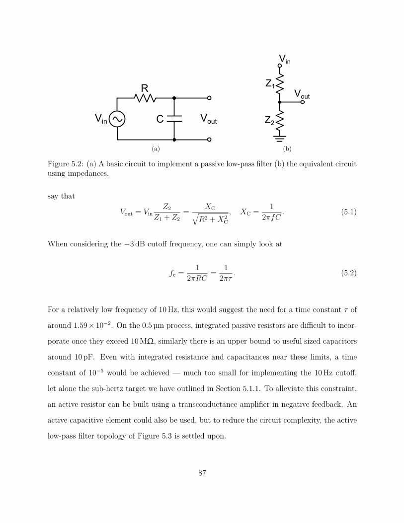
Vin
R
C Vout
(a)
Vin
Vout
Z1
Z2
(b)
Figure 5.2: (a) A basic circuit to implement a passive low-pass filter (b) the equivalent circuitusing impedances.
say that
Vout = Vin
Z2
Z1 + Z2
=XC
√
R2 + X2C
, XC =1
2πfC. (5.1)
When considering the −3 dB cutoff frequency, one can simply look at
fc =1
2πRC=
1
2πτ. (5.2)
For a relatively low frequency of 10 Hz, this would suggest the need for a time constant τ of
around 1.59 × 10⁻². On the 0.5 µm process, integrated passive resistors are difficult to incor-
porate once they exceed 10 MΩ, similarly there is an upper bound to useful sized capacitors
around 10 pF. Even with integrated resistance and capacitances near these limits, a time
constant of 10−5 would be achieved — much too small for implementing the 10 Hz cutoff,
let alone the sub-hertz target we have outlined in Section 5.1.1. To alleviate this constraint,
an active resistor can be built using a transconductance amplifier in negative feedback. An
active capacitive element could also be used, but to reduce the circuit complexity, the active
low-pass filter topology of Figure 5.3 is settled upon.
87

Vout
Itune
Vingm3
C
Figure 5.3: Implementing a low-pass filter using a current conveyor as an active element torealize a large resistance.
The input impedance of a transconductance amplifier in negative feedback is simply 1gm
,
which can be adjusted by tuning IBias. As reported in the jump resonance study, we have
designed an amplifier that can tune between 0.8 nS to 32 nS of transconductance with IBias
in the single digit nano amperes. Thus, with a simple negative feedback transconductance
amplifier we can get resistance on the order of 1 GΩ, thus giving a time constant on the order
of 10−2 when combined with a large passive capacitor. As an extension to this approach,
it may be possible to replace the capacitor with an active capacitor as well, which could
multiply the effective capacitance by as much as 105 [86]. With such an extension, the time
constant τ would be on the order of 103, yielding a cutoff frequency less than 1 mHz. Using
the equivalent noise model for a transconductor, where
∆vn2
∆f= EN × 4kT
1
gm
, (5.3)
and assuming that supply voltage excess (EV) and supply current excess (EI) factors are
unity, then the following equations will detail the active low-pass filer of Figure 5.3. Of note
is that the power dissipation of this filter when configured to have a signal-to-noise ratio of
88
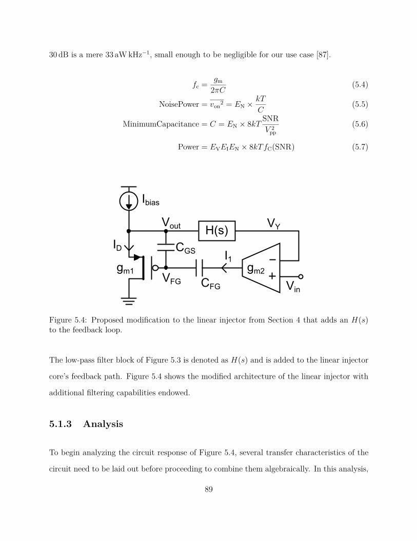
30 dB is a mere 33 aW kHz−1, small enough to be negligible for our use case [87].
fc =gm
2πC(5.4)
NoisePower = von2 = EN × kT
C(5.5)
MinimumCapacitance = C = EN × 8kTSNR
V 2pp
(5.6)
Power = EVEIEN × 8kTfC(SNR) (5.7)
gm1VFG
Ibias
CFG
VoutH(s)
gm2
I1
VY
Vin
CGSID
Figure 5.4: Proposed modification to the linear injector from Section 4 that adds an H(s)to the feedback loop.
The low-pass filter block of Figure 5.3 is denoted as H(s) and is added to the linear injector
core’s feedback path. Figure 5.4 shows the modified architecture of the linear injector with
additional filtering capabilities endowed.
5.1.3 Analysis
To begin analyzing the circuit response of Figure 5.4, several transfer characteristics of the
circuit need to be laid out before proceeding to combine them algebraically. In this analysis,
89

H(s) is implemented using Figure 5.3, and its capacitance will be denoted by CY, the Vout
as VY and the Vin is the same net as Vout of Figure 5.4.
Vout = (Ib − Igs − ID)1
sCFG
(5.8)
VY = IY
1
sCy
(5.9)
IFG = (VX − VFG)1
sCFG
(5.10)
Igs = sCgs(VFG − Vout) (5.11)
ID = g1VFG (5.12)
IY = g3(Vout − VY) (5.13)
IX = (Vin − VY) g2 = g2 (Vin − IY/sCY) = g2Vin − g2g3
sCY
(Vout − VY) (5.14)
VX = IX
(
1
sCFG
)
=g2
sCFG
(Vin − Vout) (5.15)
By merging these expressions, the following circuit response for the output voltage is derived:
Vout = (Ib − (VFG − Vout) sCgs − g1VFG) /sCL. (5.16)
Assume g1 is an ideal source-follower ∴ Vout ≡ VFG → Ib = IFG. Combining several of the
previous equations into a single expression:
Vout =1
sCL
(
sCFG
[
g2
sCFG
(
Vin − Vout
1 + CY/g3
)
− Vout
]
− g1Vout
)
. (5.17)
90

Expand the terms and consolidating the expression will result in the final transfer function
detailed in (5.22). Keeping the denominator common, one can observe that there is a low-
pass component (g2g3) and a high-pass component (sg2CLCY).
Vout =sg2CFG
s2CLCFG
Vin −(
sg2CFG
s2CLCFG
)
(
Vout
1 + sCY/g3
)
− sCFG
sCL
Vout − g1
sCL
Vout (5.18)
Vout
[
1 +g1
sCL
+CFG
CL
+g2
sCL
(
1
1 + sCY/g3
)]
=g2
sCL
Vin (5.19)
Vout
Vin
=(
g2
sCL
)
÷(
1 +CFG
CL
+g2
sCL + s2CLCY/g3
)
(5.20)
=g2
sCFG + sCL +g2
1 + sCLCY/g3
(5.21)
=g2g3 + sg2CLCY
s2 (CFGCLCY + C2LCY) + sg3 (CFG + CL) + g2g3
(5.22)
Plugging in nominal values for the capacitance and transconductances as simulated on an
extracted layout view of the circuit, the bode plot of Figure 5.5 is generated. The values of
g2 =1 n, g3 =20 n, CFG =1 pF, CL =1 pF, and CY =1.28 pF results in exactly 500 mHz as the
−3 dB cutoff frequency.
5.2 Measurement Results
5.2.1 Single Configuration
The chip was designed in using Cadence tools and sent to MOSIS for fabrication with ON
Semiconductor’s 0.5 µm process. A micrograph giving a chip-level view of the fabricated
91

10-1 100 101 102 103
Frequency (Hz)
-70
-60
-50
-40
-30
-20
-10
0
Gain
(dB
)
g1=1.000e+00g2=1.000e-12g3=2.000e-11-3dB at 0.5 Hz
Figure 5.5: Bode plot for Figure 5.4 showing a low-pass response.
die is given as Figure 5.6. For testing, a computer was used to interface with a Rigol
function generator, a Tektronix oscilloscope, a Keithley SMU, and a custom test station. In
Figure 5.7, the input signal to the chip is shown in blue, and the buffered analog output of a
single channel is plotted in orange. To get this response, the input was configured to have a
500 mV peak-to-peak amplitude and a sinusoidal shape with frequency 34.61 Hz. The active
resistor element of Figure 5.4 is tuned by Itune, which is controlled through a PMOS current
source with a gate bias of 3.4 V. The entire chip was operating on a supply voltage of 4 V
from the SMU. The output is measured on the 8 bit oscilloscope that was programmed to
have a window size approximately equal to 10 periods of the input sin wave.
92

Figure 5.6: A micrograph of the fabricated chip on the 0.5 µm CMOS process by ON Semi-conductor through MOSIS.
What Figure 5.7 shows is that there is some amount of gain present in the channel configu-
ration, and that it is not a one-to-one transfer function. To better investigate the circuit be-
havior under these biasing conditions, the input frequency was modulated between 500 mHz
and 100 kHz. In Figure 5.8, Figure 5.9, and Figure 5.10, the response at select frequencies
(denoted by the text label near the top of each subplot) is presented. To save space, the
y-axis has been fixed to 1 V to 2.2 V and the x-axis is selected to show approximately two
93
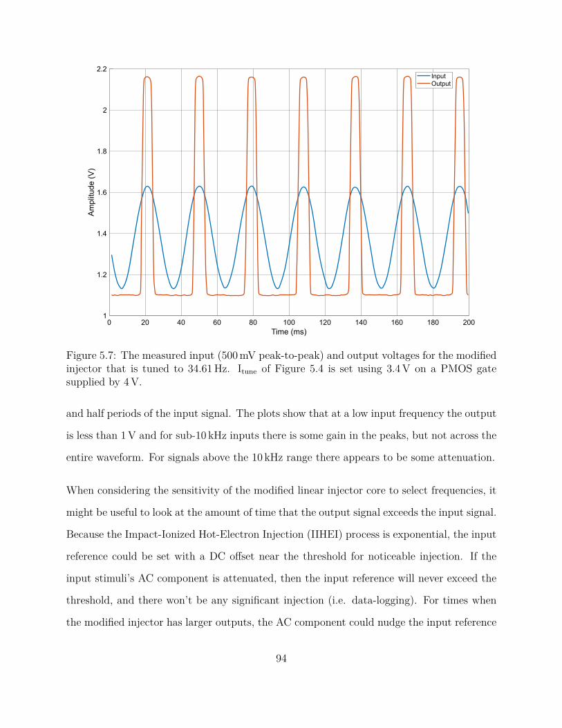
0 20 40 60 80 100 120 140 160 180 200
Time (ms)
1
1.2
1.4
1.6
1.8
2
2.2
Am
plit
ud
e (
V)
InputOutput
Figure 5.7: The measured input (500 mV peak-to-peak) and output voltages for the modifiedinjector that is tuned to 34.61 Hz. Itune of Figure 5.4 is set using 3.4 V on a PMOS gatesupplied by 4 V.
and half periods of the input signal. The plots show that at a low input frequency the output
is less than 1 V and for sub-10 kHz inputs there is some gain in the peaks, but not across the
entire waveform. For signals above the 10 kHz range there appears to be some attenuation.
When considering the sensitivity of the modified linear injector core to select frequencies, it
might be useful to look at the amount of time that the output signal exceeds the input signal.
Because the Impact-Ionized Hot-Electron Injection (IIHEI) process is exponential, the input
reference could be set with a DC offset near the threshold for noticeable injection. If the
input stimuli’s AC component is attenuated, then the input reference will never exceed the
threshold, and there won’t be any significant injection (i.e. data-logging). For times when
the modified injector has larger outputs, the AC component could nudge the input reference
94
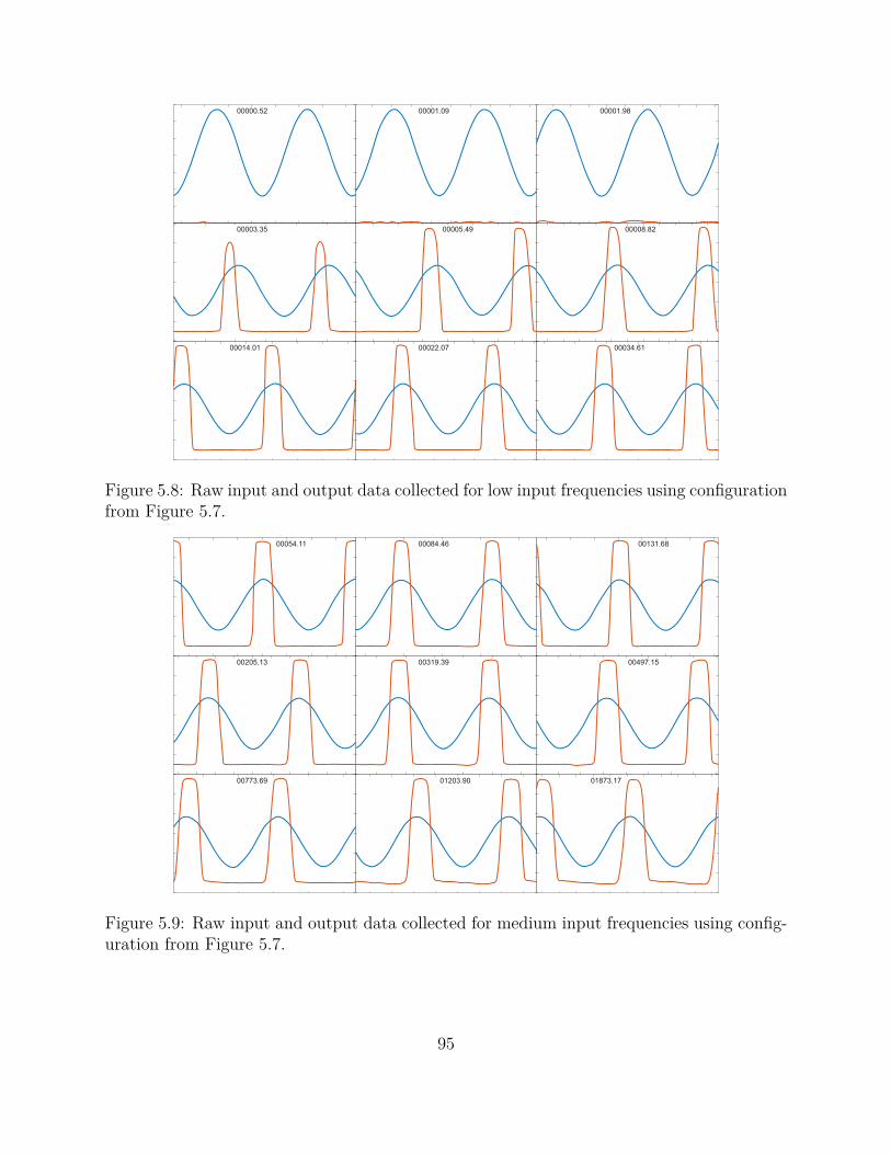
00000.52 00001.09 00001.98
00003.35 00005.49 00008.82
00014.01 00022.07 00034.61
Figure 5.8: Raw input and output data collected for low input frequencies using configurationfrom Figure 5.7.
00054.11 00084.46 00131.68
00205.13 00319.39 00497.15
00773.69 01203.90 01873.17
Figure 5.9: Raw input and output data collected for medium input frequencies using config-uration from Figure 5.7.
95

02914.34 04534.09 07053.92
10974.00 17072.42 26559.67
41318.88 64279.66 99999.50
Figure 5.10: Raw input and output data collected for high input frequencies using configu-ration from Figure 5.7.
high enough that a recordable amount of injection occurs. Therefore, plots showing when the
output exceeds the input amplitude are shown in Figure 5.11, Figure 5.12, and Figure 5.13.
Similar to the previous figures, the input stimuli’s frequency is shown near the top of each
subplot in black text. The blue text indicates the ratio of time that the output exceeds the
input.
5.2.2 Aggregate Plots
Several biasing conditions of the modified core were tested. Similar to the basic configuration
of Figure 5.7, Figure 5.14 decreases the gate voltage that controls Itune to 3.0 V, thereby
increasing the supply current to the transconductance. Figure 5.15 further decreases the
gate voltage to 2.6 V. Just showing the lower input frequencies in these two figures, it is
apparent that the filtering characteristics have changed.
96

00
00000.52
00
00001.09
00
00001.98
0.127020.12702
00003.35
0.16120.1612
00005.49
0.160210.16021
00008.82
0.185820.18582
00014.01
0.185380.18538
00022.07
0.194670.19467
00034.61
Figure 5.11: True or false plots showing when output exceeds input for low input frequenciesusing configuration from Figure 5.7.
0.19860.1986
00054.11
0.194140.19414
00084.46
0.199750.19975
00131.68
0.206770.20677
00205.13
0.206280.20628
00319.39
0.227020.22702
00497.15
0.229870.22987
00773.69
0.227310.22731
01203.90
0.226270.22627
01873.17
Figure 5.12: True or false plots showing when output exceeds input for medium input fre-quencies using configuration from Figure 5.7.
97

0.217510.21751
02914.34
0.169730.16973
04534.09
0.120850.12085
07053.92
00
10974.00
00
17072.42
00
26559.67
00
41318.88
00
64279.66
00
99999.50
Figure 5.13: True or false plots showing when output exceeds input for high input frequenciesusing configuration from Figure 5.7.
00000.52 00001.09 00001.98
00003.35 00005.49 00008.82
00014.01 00022.07 00034.61
Figure 5.14: Similar to Figure 5.8, but with a larger Itune.
98

00000.52 00001.09
00001.98
00003.3500005.49 00008.82
00014.0100022.07 00034.61
Figure 5.15: Similar to Figure 5.14, but with a larger Itune.
To approximate the useful transfer characteristics of different configurations, Figure 5.16
plots the mean ratio of when the output exceeds the input (as collected from Figure 5.11,
Figure 5.12, and Figure 5.13). One can observe that at low Itune (plotted in yellow as 3.40)
there is a flat bandpass like response. For a slightly higher current (orange, 3.0 in figure),
the transfer function appears to be a low-pass, or perhaps a bandpass with the lower cutoff
frequency below 500 mHz. Using even more current (blue, 2.60 in figure), the bandpass is
no longer flat, and sharper trends are observed. Figure 5.17 repeats the test results for a
smaller input amplitude of 100 mHz and Figure 5.18 considers the case of a larger input
amplitude of 1 V. Note that some data points in Figure 5.17 may not have been recorded
properly during the automated testing that iterated over thousands of test configurations
across several days. It should also be noted that these plots are not the same as traditional
transfer plots as in the bode plot of Figure 5.5, thus a direct comparison cannot be drawn.
99
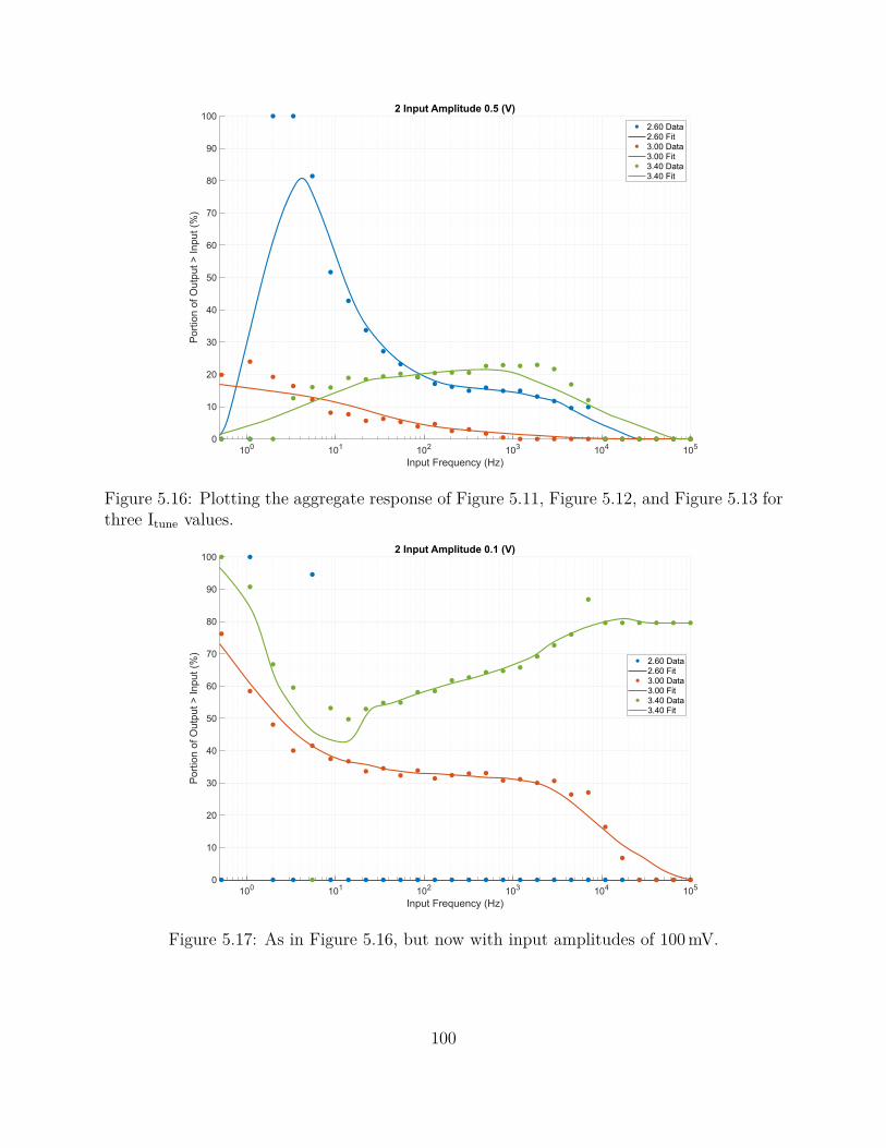
100 101 102 103 104 105
Input Frequency (Hz)
0
10
20
30
40
50
60
70
80
90
100
Port
ion o
f O
utp
ut >
Input (%
)
2 Input Amplitude 0.5 (V)
2.60 Data2.60 Fit3.00 Data3.00 Fit3.40 Data3.40 Fit
Figure 5.16: Plotting the aggregate response of Figure 5.11, Figure 5.12, and Figure 5.13 forthree Itune values.
100 101 102 103 104 105
Input Frequency (Hz)
0
10
20
30
40
50
60
70
80
90
100
Port
ion o
f O
utp
ut >
Input (%
)
2 Input Amplitude 0.1 (V)
2.60 Data2.60 Fit3.00 Data3.00 Fit3.40 Data3.40 Fit
Figure 5.17: As in Figure 5.16, but now with input amplitudes of 100 mV.
100
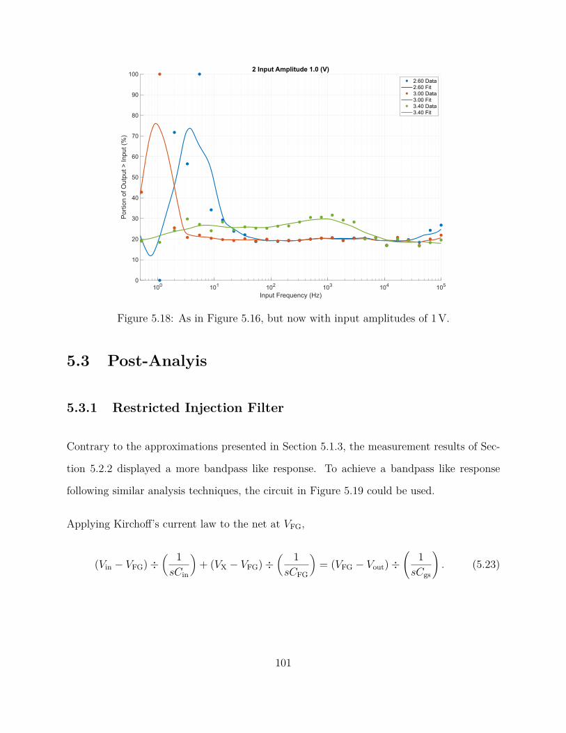
100 101 102 103 104 105
Input Frequency (Hz)
0
10
20
30
40
50
60
70
80
90
100
Port
ion o
f O
utp
ut >
Input (%
)
2 Input Amplitude 1.0 (V)
2.60 Data2.60 Fit3.00 Data3.00 Fit3.40 Data3.40 Fit
Figure 5.18: As in Figure 5.16, but now with input amplitudes of 1 V.
5.3 Post-Analyis
5.3.1 Restricted Injection Filter
Contrary to the approximations presented in Section 5.1.3, the measurement results of Sec-
tion 5.2.2 displayed a more bandpass like response. To achieve a bandpass like response
following similar analysis techniques, the circuit in Figure 5.19 could be used.
Applying Kirchoff’s current law to the net at VFG,
(Vin − VFG) ÷(
1
sCin
)
+ (VX − VFG) ÷(
1
sCFG
)
= (VFG − Vout) ÷(
1
sCgs
)
. (5.23)
101

gm1VFG
VRef
Ibias
CFG
VoutH(s)
gm2
I1
VY
Vx
VinCin
CGSID
Figure 5.19: An alternative input as compared to that of Figure 5.4.
Again, assuming that g1 is an ideal source-follower ∴ Vout ≡ VFG, (5.23) simplifies to:
0 = sCinVin − VFGsCin + sCFGVX − VFGsCFG, (5.24)
sCinVin + sCFGVX = VFG(sCin + sCFG). (5.25)
Additionally, the voltage at the output of the transconductance g2 is approximated as:
VX =g2
sCFG
(VRef − H(s)VFG) . (5.26)
Using this approximation, (5.25) expands thusly
sCinVin + g2VRef − g2H(s)VFG = VFG(sCin + sCFG) (5.27)
g2VRef + sCinVin = VFG [s (Cin + CFG) + g2H(s)] (5.28)
g2VRef + sCinVin = g2VFG
[
s
g2
(Cin + CFG) + H(s)
]
(5.29)
102

Finally, the output expression for Figure 5.19 is given as:
Vout =VRef
sg2
(Cin + CFG + H(s)+
sCinVin/g2
sg2
(Cin + CFG + H(s). (5.30)
10-1 100 101 102 103
Frequency (Hz)
-25
-20
-15
-10
-5
0
5
Gain
(dB
)
g1=2.000e-11g2=2.000e-11g3=2.000e-11
Figure 5.20: Bode plot showing the response for the conditions given in Figure 5.19.
The resulting bode plot is presented in Figure 5.20, and the simulated response appears to
be a low-pass filtering, but could also be used as a bandpass filter near 15 Hz. It is likely that
these approximations in the analysis are neglecting important capacitance or other feedback
mechanisms that would cause the transfer functions to have a much stronger high-pass
element as observed during measurement. These results may appear in future literature [88].
103

5.3.2 Improved Sensitivity
The alternative configuration of Figure 5.19 also introduces an interesting method for pro-
viding improved input stimuli sensitivity. When starting this dissertation, it was envisioned
that the entire sensing platform, including wireless interrogation, would operate in a self-
powered mode. Since that time, digital circuits have improved 33 fold with respect to the
number of operations per watt (looking at GFLOPS/W of the top supercomputer on Green
500). Commercial entities have also vastly improved the energy efficiency of wireless commu-
nication as smartphones became common place and Moore’s law marched on. Accordingly,
in Chapter 6, the platform has moved from completely self-powered solution, to one that
relies on battery-powered wireless communication. Leveraging the already present battery
allows the PFG to power onboard references and even its feedback amplifier whilst sipping
mere nano amperes. Even with an always-on reference and amplifier drawing current, most
battery’s operational lifespan would be dominated by the self-dischage leakage current. One
of the best primary lithium-metal cells on the market (Tadiran LiSOCl2) has a shelf life of
40 years, thus a 100 mAh battery has a constant leakage current of approximately 300 nA.
In the case of rechargeable Lithium-ion and other more common batteries, this leakage rate
is several times larger.
With the PFG chip configured as constantly-on, an input stimuli can capacitively couple to
the floating-gate to directly modulate the gate-source voltage. If the modulation increases
the voltage, it will increase the chance of IIHEI occurring. This has been verified as shown in
Figure 5.21, for three conditions for multiple injection cycles. For the null case, 1 V is applied
to Cin, but the feedback of gm2 is disabled, the resulting green plot shows no data-logging. For
the red plot, injection was enabled, but the input to the capacitor was tied to ground. It will
inject since the reference voltage is 5.823 V, albiet at a reduced rate as tested in Chapter 4.
104
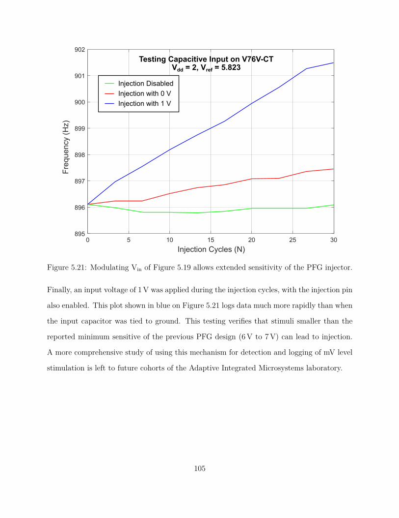
0 5 10 15 20 25 30895
896
897
898
899
900
901
902
Fre
qu
ency (
Hz)
Injection Cycles (N)
Testing Capacitive Input on V76V-CTVdd = 2, Vref = 5.823
Injection Disabled
Injection with 0 V
Injection with 1 V
Figure 5.21: Modulating Vin of Figure 5.19 allows extended sensitivity of the PFG injector.
Finally, an input voltage of 1 V was applied during the injection cycles, with the injection pin
also enabled. This plot shown in blue on Figure 5.21 logs data much more rapidly than when
the input capacitor was tied to ground. This testing verifies that stimuli smaller than the
reported minimum sensitive of the previous PFG design (6 V to 7 V) can lead to injection.
A more comprehensive study of using this mechanism for detection and logging of mV level
stimulation is left to future cohorts of the Adaptive Integrated Microsystems laboratory.
105

Chapter 6
Transfer To Practice
Deploying the Analog Frontend
6.1 Piezoelectric Transducer
Before the Piezoelectric-Floating-Gate (PFG) sensor can be deployed, it needs to be coupled
with a suitable piezoelectric transducer [89]. In this section, testing done in conjunction with
Professor Nizar Lajnef’s research team at Michigan State University, on the characteristics of
potential piezoelectrics, is presented. Specifically, this chapter will focus on the deployment
of the analog frontends for Structural Health Monitoring (SHM) applications. Based on
discussions with these domain experts, many target applications would require the detection
of micro-strain energy from structural elements such as steel beams, or asphalt. The type
of transducer that is coupled to the PFG sensor will affect the amount of information that
is logged. In a controlled laboratory setting, the behavior of three different piezoelectric
transducers is investigated. Primarily, we focus on piezoelectric ceramic discs (PZTs) that
were sourced from STEMINC Incorporated, with properties as specified in Table 6.1. For
the purpose of this section, the considered piezoelectric discs are labeled as PZT1, PZT2,
and PZT3. PZT1 and PZT3 have the same diameter of 20 mm, and PZT2 is larger with a
106

diameter of 25 mm. PZT2 and PZT3 have the same material thickness (height) of 700 µm,
and PZT1 has a larger height of 800 µm. In Figure 6.1a, a diagram of the testing apparatus
is illustrated, and Figure 6.1b shows how a test specimen is placed in an MTS device for
precision loading. Figure 6.1c gives a close-up of the PZTs affixed to the an aluminum test
specimen of dimensions 457.2 mm×50.8 mm×12.7 mm (18 in×2 in×1/2 in). The specimen
will undergo a four-point bending test, with measurement results presented in the following
subsections.
Table 6.1: Piezoelectric Specifications
Parameter Unit Symbol Value
ElectromechanicalCoupling
Coefficient
Kp 0.58– Kt 0.45
K31 0.34
FrequencyConstant
Np 2200
Hz m Nt 2070
N31 1680
PiezoelectricConstant
10 pm V−1d33 320
d31 -140
10 mm N−1
g33 25
g31 -11.0
ElasticConstant
1010 N m−2 Y33 7.3
Y11 8.6
MechanicalQuality Factor
– Qm 1800
DielectricConstant at 1 kHz eT33/e0 1400
Dissipation Factor % at 1 kHz tan δ 0.4
CurieTemperature
C Tc 320
Density g cm−3 r 7.9
107

(a)
(b) (c)
Figure 6.1: (a) A diagram of the testing apparatus, (b) an image of the actual MTS setup,and (c) closeup of the PZTs affixed to the sample under strain.
In this four-point bending test, the strain is assumed to be constant between the load appli-
cation points, with strain amplitude given as:
ηsurf =3FA
Ebh2, (6.1)
108

where F is the applied force, A is the coordinate of the first inner clamp with respect to the
first outer clamp, b is the width of the specimen under test, h is the height, and E is the
elastic modulus.
Figure 6.2: Plotting the voltage generated by the PZT samples (i.e. Sensor Voltage) as afunction of the induced strain.
The voltages generated from the PZTs are logged using an NI9220, similarly the strain gage
behavior is logged using an NI9236, both devices were purchased from National Instruments.
Additionally, each PZT is connected to a PFG sensor (with an equivalent impedance of
50 MΩ) as depicted in the diagram of Figure 6.1a. The testing load is applied using an
MTS servo-hydraulic machine in a displacement-controlled mode, with a cyclic displacement
applied for each test iteration. The number of cycles for the input load was initially started
at 50, with a cycle frequency of 2 Hz, and the number of cycles was gradually increased
until the first channel of the PFG began to log data. This procedure of programmaticly
increasing the number of cycles was repeated for each subsequent channel of the PFG until
all seven channels would log some data due to the input stimuli. The actual strain levels are
simultaneously recorded via the strain gage during these testing cycles, and a plot showing
109
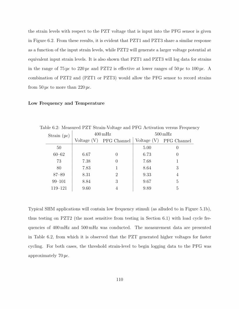
the strain levels with respect to the PZT voltage that is input into the PFG sensor is given
in Figure 6.2. From these results, it is evident that PZT1 and PZT3 share a similar response
as a function of the input strain levels, while PZT2 will generate a larger voltage potential at
equivalent input strain levels. It is also shown that PZT1 and PZT3 will log data for strains
in the range of 75 µǫ to 220 µǫ and PZT2 is effective at lower ranges of 50 µǫ to 100 µǫ. A
combination of PZT2 and (PZT1 or PZT3) would allow the PFG sensor to record strains
from 50 µǫ to more than 220 µǫ.
Low Frequency and Temperature
Table 6.2: Measured PZT Strain-Voltage and PFG Activation versus Frequency
Strain (µǫ) 400 mHz 500 mHz
Voltage (V) PFG Channel Voltage (V) PFG Channel
50 5.00 0
60–62 6.67 0 6.73 0
73 7.38 0 7.68 1
80 7.83 1 8.64 3
87–89 8.31 2 9.33 4
99–101 8.84 3 9.67 5
119–121 9.60 4 9.89 5
Typical SHM applications will contain low frequency stimuli (as alluded to in Figure 5.1b),
thus testing on PZT2 (the most sensitive from testing in Section 6.1) with load cycle fre-
quencies of 400 mHz and 500 mHz was conducted. The measurement data are presented
in Table 6.2, from which it is observed that the PZT generated higher voltages for faster
cycling. For both cases, the threshold strain-level to begin logging data to the PFG was
approximately 70 µǫ.
110

Table 6.3: Measured PZT Strain-Voltage and PFG Activation versus Temperature
Strain (µǫ) 20 C −20 C
Voltage (V) PFG Channel Voltage (V) PFG Channel
50–51 7.37 1 7.04 0
62 8.50 2 7.75 1
72–73 9.38 4 8.67 2
82–83 9.80 5 9.42 4
92–94 10.05 6 9.77 5
103 9.91 5
An additional consideration for deployment in real-world applications is the temperature
effects on PZT performance. It is a well-known fact that typical piezoelectric materials
will show output response sensitivity to temperature (typically being less responsive in the
cold for PZT), and here it is verified that lower temperatures won’t significantly hinder
the data logging capabilities of the PFG sensor. Again, the testing apparatus follows that
of Figure 6.1 and the preceding sections. The main difference being that the piezoelectric
transducer element is protected from environmental conditions using “Flex Seal,” a spray-on
rubberized sealant. The coating provides protection against water, humidity, air, and other
environmental factors that could cause damage such as corrosion to present itself on the
PZT. We repeat the 500 mHz testing as before, but this time at 20 C and −20 C, with
the resulting plots and data shown in Table 6.3. A shift in the channel activation to higher
strains for lower temperature is observed, yet with the selected PZT, the PFG remains a
viable sensor for the strain levels of interest at either temperature.
Cabling Effects
An important consideration is that the PFG will need to be wired to the piezoelectric trans-
ducer that was selected. The in-lab connections are not rated for the extreme conditions of
111

the environment that will be experienced in deployment situations, be it the sub-zero temper-
atures of winters, or the greater than 100 C during asphalt compaction. The type of wiring
could have a noticeable affect on the sensor performance, as the capacitance and electrical
resistance of the wires could vary depending on the gauge, shielding, or wire arrangement of
a cable. Under consideration is the C0744A.41.10 multiconductor (eight wires) cable from
General Cable, which uses 24 AWG stranded copper as the conducting wires with 0.0320 in
of poly-vinyl chloride (PVC) insulation with a rated operational temperature range of 20 C
to 80 C and inter-wire capacitance of 30 pF/ft and wire-to-shield capacitance of 55 pF/ft.
This cable was chosen for its low-cost and high availability (it is similar to cables used for
Ethernet) as well as the low capacitance offered by thin conductors. To test the effects of
a more robust cable, the C8101.41.03, also from General Cable, was sampled. The cable
only has two conductors of 18 AWG each and a much more robust 0.0160 in Fluorinated
Ethylene Propylene (FEP) jacket insulation with operational ratings of −40 C to 150 C
and inter-wire capacitance of 51 pF/ft and wire-to-shield capacitance of 91 pF/ft.
Testing was carried out in the low input frequency and room temperature configuration of the
four-point bending test. From recorded threshold strain levels and voltage generated, it was
found that for PZT2 the average difference in PFG channel thresholds between the two cables
was about 0.86 µǫ or 15.7 mV, similarly for PZT3 the average differences were 1.85 µǫ and
10.0 mV — that is to say that the cables had negligible affect on the threshold performance
of the PFG sensors. Although the performance was not degraded by the choice of cabling, it
would be important to source cables that are rated for the expected deployment environment,
which could exclude the PVC jacket insulation if freezing conditions are expected.
112

6.1.1 Piezoelectric-Floating-Gate Verification
Previously, in Chapter 4, Section 4.2, and [90], the Piezoelectric-Floating-Gate (PFG) sen-
sor’s characteristics were presented, when tested with ideal sources, such as function gener-
ators or other electrically-controlled systems. In this section, the PFG is connected to the
piezoelectric as selected following the testing in Section 6.1, and the functionality is verified.
The first result is presented in Table 6.4, which shows the approximate voltages generated
by the PZT2 (henceforce, PZT) transducer that activated each PFG channel.
Table 6.4: Approximate Activation Thresholds for PFG Channels
Voltage (V) PFG Channel
<7.75 0
7.75 1
8.22 1–2
8.69 1–3
9.15 1–4
9.62 1–5
10.09 1–6
10.56 1–7
Figure 6.3 shows example injection profiles for four different floating gates on a sensor pro-
totype. Following the test procedure described in Section 6.1, in this sample data shown
in Figure 6.3, the input loading is increased until the response strains hit a level sufficient
to activate the first three memory cells (noted as Strain Level 1). Then, the loading is
gradually increased until the fourth channel is activated. At each strain level, the input
loading is cycled for fifty iterations to show the injection profile. The test results show good
agreement between fabricated chips, and verifies the concept of the PFG sensor logging cu-
mulative strain histories. As discussed in Section 4, the tuning resistance is lowered for this
113

0 10 20 30 40Loading Cycles
85
90
95
100
Rem
ain
ing M
em
ory
(%
)
Strain Level 1Strain Level 2Strain Level 3Strain Level 4
(a)
0 10 20 30 40Loading Cycles
85
90
95
100
Rem
ain
ing M
em
ory
(%
)
Strain Level 1Strain Level 2Strain Level 3Strain Level 4
(b)
0 10 20 30 40Loading Cycles
85
90
95
100
Rem
ain
ing M
em
ory
(%
)
Strain Level 1Strain Level 2Strain Level 3Strain Level 4
(c)
0 10 20 30 40Loading Cycles
85
90
95
100
Rem
ain
ing M
em
ory
(%
)
Strain Level 1Strain Level 2Strain Level 3Strain Level 4
(d)
Figure 6.3: Verifying the injection profile with four different fabricated chips, there is somevariation between chips due to fabrication mismatch.
prototype to observe changes with tens of cycles. It should be noted that this dissertation
focuses on the electrical design of the PFG sensor, and the task of data interpretation has
been left to domain experts, primarily in civil engineering, with results widely reported in
literature [91, 92, 93, 94, 95, 96, 97, 98, 99, 100].
6.1.2 Destructive Structural Testing
The selection of PZT, and verification of compatibility with the PFG sensor was conducted
under the assumption of a structure that experiences gradual decay in the integrity of steel
114
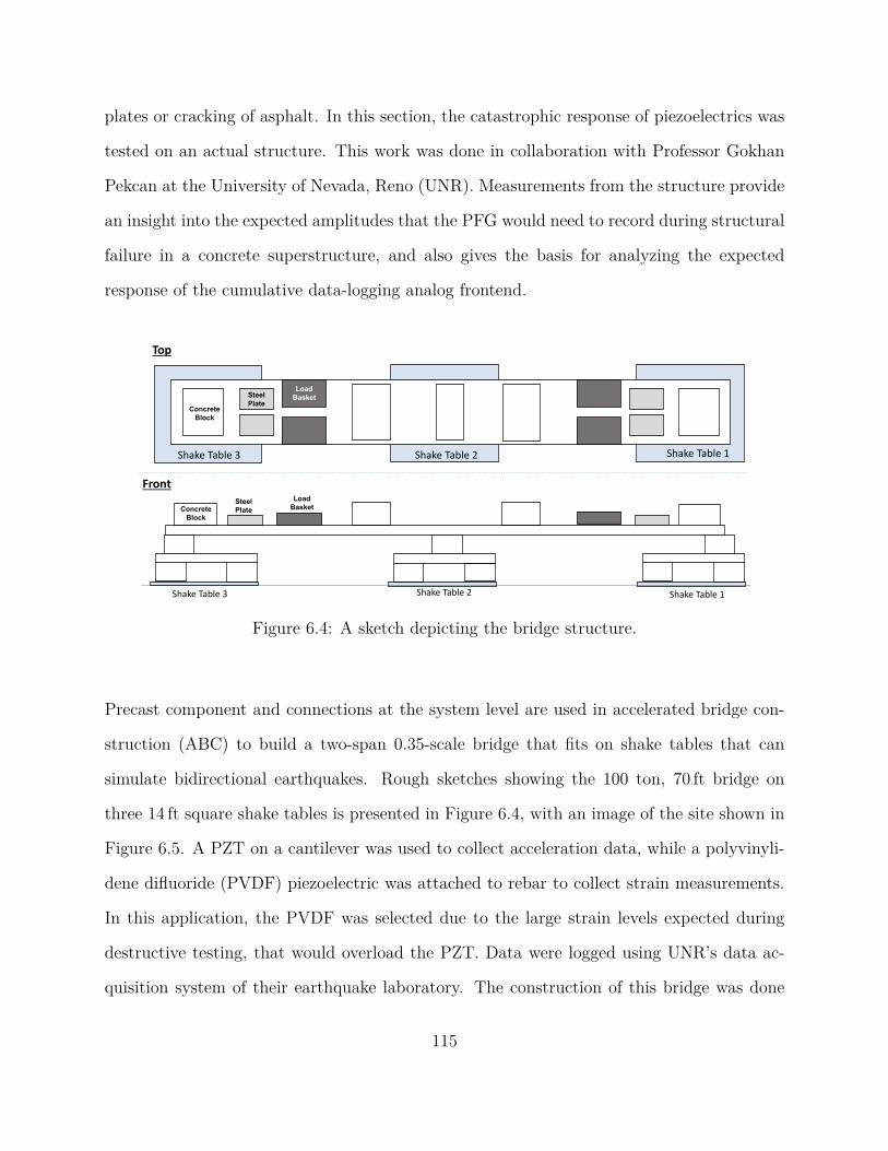
plates or cracking of asphalt. In this section, the catastrophic response of piezoelectrics was
tested on an actual structure. This work was done in collaboration with Professor Gokhan
Pekcan at the University of Nevada, Reno (UNR). Measurements from the structure provide
an insight into the expected amplitudes that the PFG would need to record during structural
failure in a concrete superstructure, and also gives the basis for analyzing the expected
response of the cumulative data-logging analog frontend.
Top
Front
Shake Table 2
Concrete
Block
Steel
Plate
Load
Basket
Shake Table 1Shake Table 3
Shake Table 3 Shake Table 2 Shake Table 1
Concrete
Block
Steel
Plate
Load
Basket
Figure 6.4: A sketch depicting the bridge structure.
Precast component and connections at the system level are used in accelerated bridge con-
struction (ABC) to build a two-span 0.35-scale bridge that fits on shake tables that can
simulate bidirectional earthquakes. Rough sketches showing the 100 ton, 70 ft bridge on
three 14 ft square shake tables is presented in Figure 6.4, with an image of the site shown in
Figure 6.5. A PZT on a cantilever was used to collect acceleration data, while a polyvinyli-
dene difluoride (PVDF) piezoelectric was attached to rebar to collect strain measurements.
In this application, the PVDF was selected due to the large strain levels expected during
destructive testing, that would overload the PZT. Data were logged using UNR’s data ac-
quisition system of their earthquake laboratory. The construction of this bridge was done
115
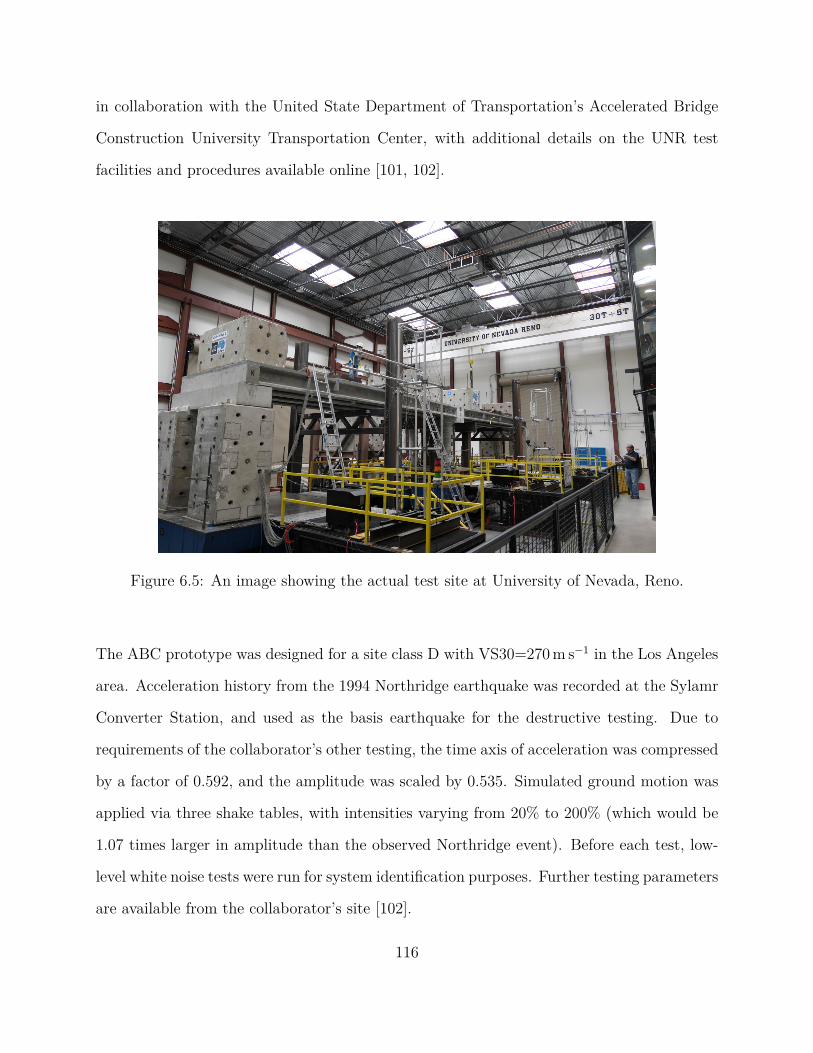
in collaboration with the United State Department of Transportation’s Accelerated Bridge
Construction University Transportation Center, with additional details on the UNR test
facilities and procedures available online [101, 102].
Figure 6.5: An image showing the actual test site at University of Nevada, Reno.
The ABC prototype was designed for a site class D with VS30=270 m s−1 in the Los Angeles
area. Acceleration history from the 1994 Northridge earthquake was recorded at the Sylamr
Converter Station, and used as the basis earthquake for the destructive testing. Due to
requirements of the collaborator’s other testing, the time axis of acceleration was compressed
by a factor of 0.592, and the amplitude was scaled by 0.535. Simulated ground motion was
applied via three shake tables, with intensities varying from 20% to 200% (which would be
1.07 times larger in amplitude than the observed Northridge event). Before each test, low-
level white noise tests were run for system identification purposes. Further testing parameters
are available from the collaborator’s site [102].
116
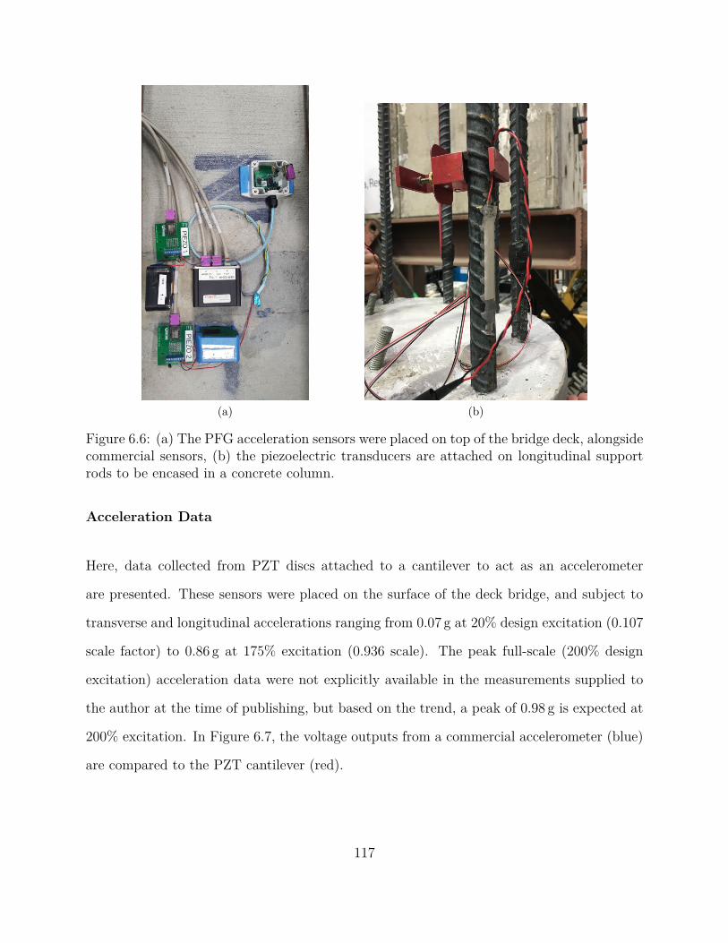
(a) (b)
Figure 6.6: (a) The PFG acceleration sensors were placed on top of the bridge deck, alongsidecommercial sensors, (b) the piezoelectric transducers are attached on longitudinal supportrods to be encased in a concrete column.
Acceleration Data
Here, data collected from PZT discs attached to a cantilever to act as an accelerometer
are presented. These sensors were placed on the surface of the deck bridge, and subject to
transverse and longitudinal accelerations ranging from 0.07 g at 20% design excitation (0.107
scale factor) to 0.86 g at 175% excitation (0.936 scale). The peak full-scale (200% design
excitation) acceleration data were not explicitly available in the measurements supplied to
the author at the time of publishing, but based on the trend, a peak of 0.98 g is expected at
200% excitation. In Figure 6.7, the voltage outputs from a commercial accelerometer (blue)
are compared to the PZT cantilever (red).
117
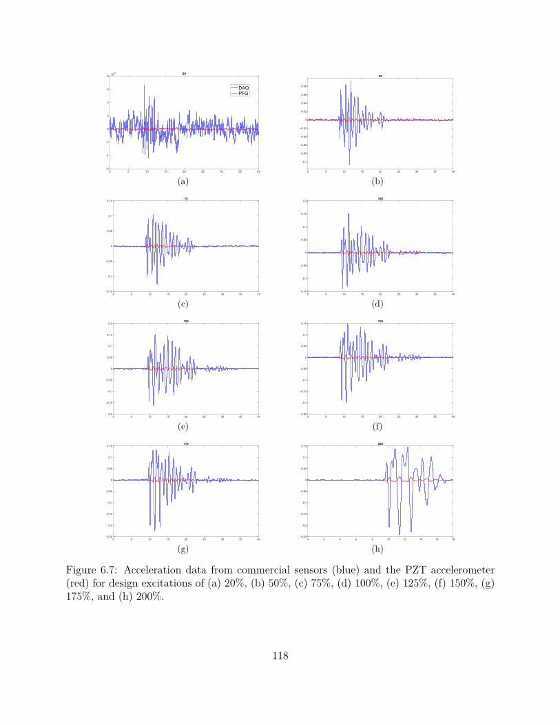
0 5 10 15 20 25 30 35 40-6
-4
-2
0
2
4
6
810-3 20
DAQ
PFG
(a)
0 5 10 15 20 25 30 35 40
-0.1
-0.08
-0.06
-0.04
-0.02
0
0.02
0.04
0.06
0.08
50
(b)
0 5 10 15 20 25 30 35 40
-0.15
-0.1
-0.05
0
0.05
0.1
0.1575
(c)
0 5 10 15 20 25 30 35 40
-0.15
-0.1
-0.05
0
0.05
0.1
0.15
0.2100
(d)
0 5 10 15 20 25 30 35 40
-0.2
-0.15
-0.1
-0.05
0
0.05
0.1
0.15
0.2125
(e)
0 5 10 15 20 25 30 35 40
-0.25
-0.2
-0.15
-0.1
-0.05
0
0.05
0.1
0.15150
(f)
0 5 10 15 20 25 30 35 40
-0.25
-0.2
-0.15
-0.1
-0.05
0
0.05
0.1
0.15175
(g)
0 2 4 6 8 10 12 14 16 18
-0.25
-0.2
-0.15
-0.1
-0.05
0
0.05
0.1
0.15200
(h)
Figure 6.7: Acceleration data from commercial sensors (blue) and the PZT accelerometer(red) for design excitations of (a) 20%, (b) 50%, (c) 75%, (d) 100%, (e) 125%, (f) 150%, (g)175%, and (h) 200%.
118
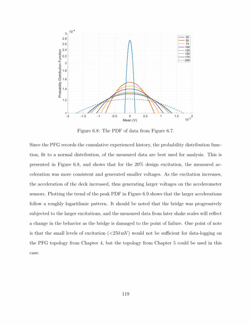
-2 -1.5 -1 -0.5 0 0.5 1 1.5 2
Mean (V) 10-3
1
1.2
1.4
1.6
1.8
2
2.2
2.4
2.6
2.8
3
Pro
ba
bili
ty D
istr
ibu
tio
n F
un
ctio
n
10-4
20 50 75100125150175200
Figure 6.8: The PDF of data from Figure 6.7.
Since the PFG records the cumulative experienced history, the probability distribution func-
tion, fit to a normal distribution, of the measured data are best used for analysis. This is
presented in Figure 6.8, and shows that for the 20% design excitation, the measured ac-
celeration was more consistent and generated smaller voltages. As the excitation increases,
the acceleration of the deck increased, thus generating larger voltages on the accelerometer
sensors. Plotting the trend of the peak PDF in Figure 6.9 shows that the larger accelerations
follow a roughly logarithmic pattern. It should be noted that the bridge was progressively
subjected to the larger excitations, and the measured data from later shake scales will reflect
a change in the behavior as the bridge is damaged to the point of failure. One point of note
is that the small levels of excitation (<250 mV) would not be sufficient for data-logging on
the PFG topology from Chapter 4, but the topology from Chapter 5 could be used in this
case.
119
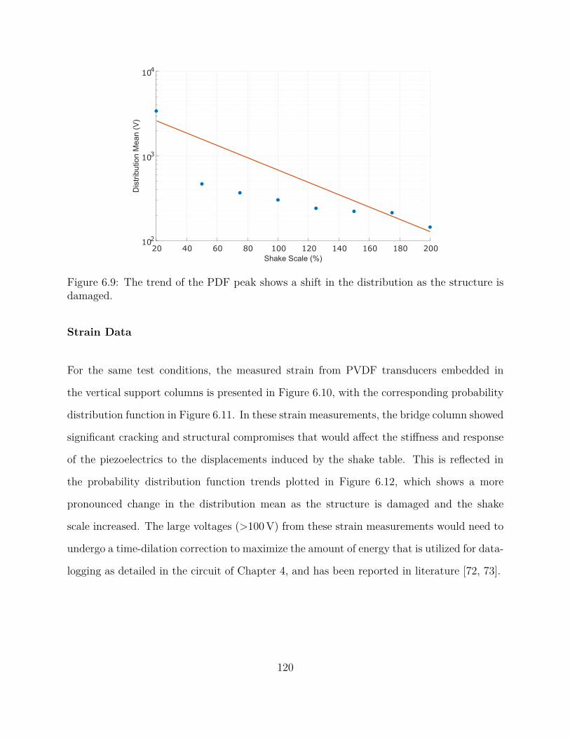
20 40 60 80 100 120 140 160 180 200
Shake Scale (%)
102
103
104
Dis
trib
utio
n M
ea
n (
V)
Figure 6.9: The trend of the PDF peak shows a shift in the distribution as the structure isdamaged.
Strain Data
For the same test conditions, the measured strain from PVDF transducers embedded in
the vertical support columns is presented in Figure 6.10, with the corresponding probability
distribution function in Figure 6.11. In these strain measurements, the bridge column showed
significant cracking and structural compromises that would affect the stiffness and response
of the piezoelectrics to the displacements induced by the shake table. This is reflected in
the probability distribution function trends plotted in Figure 6.12, which shows a more
pronounced change in the distribution mean as the structure is damaged and the shake
scale increased. The large voltages (>100 V) from these strain measurements would need to
undergo a time-dilation correction to maximize the amount of energy that is utilized for data-
logging as detailed in the circuit of Chapter 4, and has been reported in literature [72, 73].
120
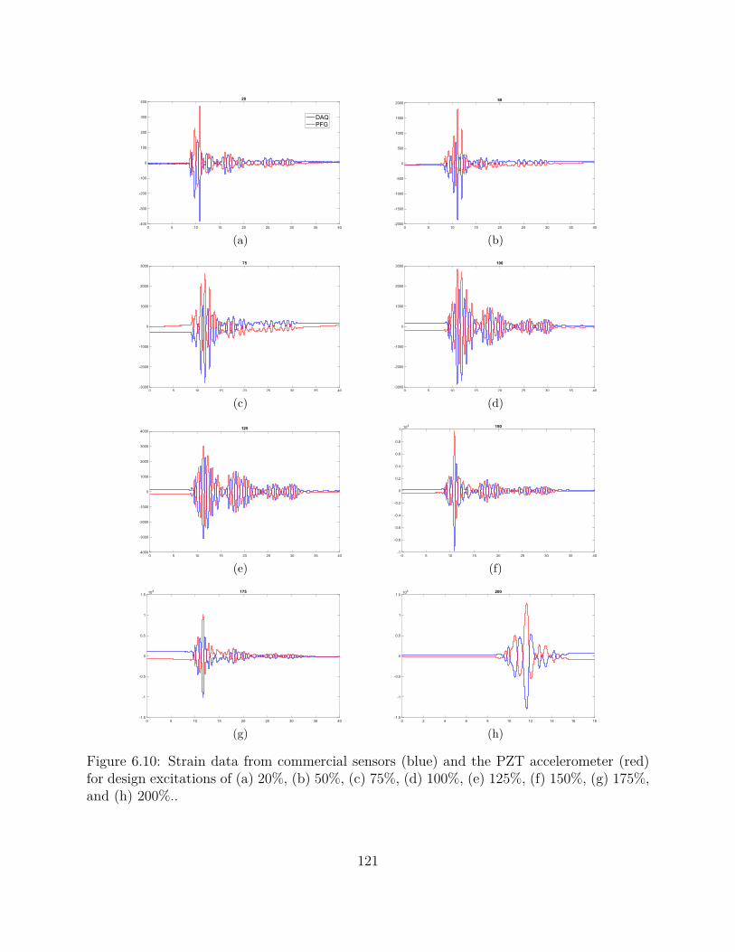
0 5 10 15 20 25 30 35 40-400
-300
-200
-100
0
100
200
300
40020
DAQ
PFG
(a)
0 5 10 15 20 25 30 35 40
-2000
-1500
-1000
-500
0
500
1000
1500
200050
(b)
0 5 10 15 20 25 30 35 40
-3000
-2000
-1000
0
1000
2000
300075
(c)
0 5 10 15 20 25 30 35 40
-3000
-2000
-1000
0
1000
2000
3000100
(d)
0 5 10 15 20 25 30 35 40
-4000
-3000
-2000
-1000
0
1000
2000
3000
4000125
(e)
0 5 10 15 20 25 30 35 40
-1
-0.8
-0.6
-0.4
-0.2
0
0.2
0.4
0.6
0.8
1104 150
(f)
0 5 10 15 20 25 30 35 40
-1.5
-1
-0.5
0
0.5
1
1.5104 175
(g)
0 2 4 6 8 10 12 14 16 18
-1.5
-1
-0.5
0
0.5
1
1.5104 200
(h)
Figure 6.10: Strain data from commercial sensors (blue) and the PZT accelerometer (red)for design excitations of (a) 20%, (b) 50%, (c) 75%, (d) 100%, (e) 125%, (f) 150%, (g) 175%,and (h) 200%..
121
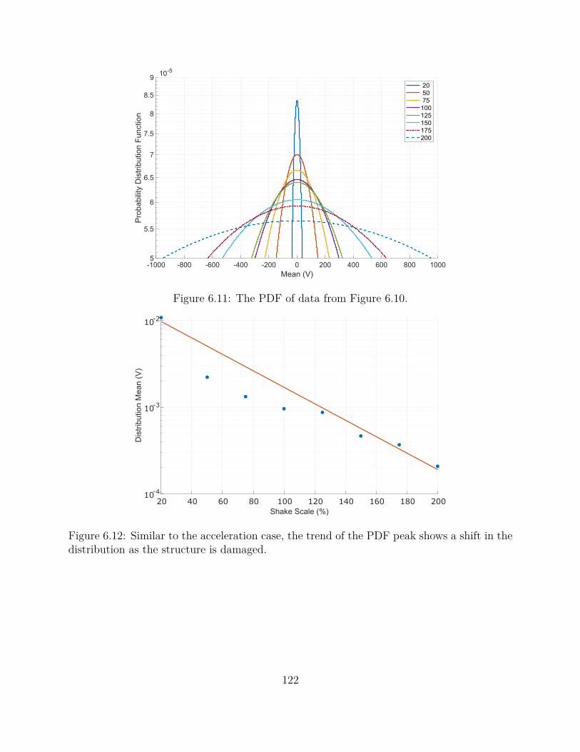
-1000 -800 -600 -400 -200 0 200 400 600 800 1000
Mean (V)
5
5.5
6
6.5
7
7.5
8
8.5
9
Pro
ba
bili
ty D
istr
ibu
tio
n F
un
ctio
n
10-5
20 50 75100125150175200
Figure 6.11: The PDF of data from Figure 6.10.
20 40 60 80 100 120 140 160 180 200
Shake Scale (%)
10-4
10-3
10-2
Dis
trib
ution M
ean
(V
)
Figure 6.12: Similar to the acceleration case, the trend of the PDF peak shows a shift in thedistribution as the structure is damaged.
122

Figure 6.13: The amount of current draw from a piezoelectric excited to 7 V varies withtemperature.
6.1.3 Energy Requirements
With respect to the amount of energy that the PFG self-powered sensor requires, the current
drawn from a piezoelectric that is mechanical stimulated to generate 7 V was measured
from −20 C to 60 C in 10 C increments. The resulting supply current plot is shown in
Figure 6.13, and tends to remain below 50 nA. In this configuration, it is expected that
one channel of the PFG is injecting, and all supporting references and injection control
circuitry is active to use 260 nW at room temperature. In earlier work for initial PFG
implementations [75] the power requirement was 200 µW, and versions ranging from 5 nW
to 800 nW have been reported [103, 104, 19]. There is still potential for optimizing these
self-powered data-logging methods into the pW scale.
123

6.2 Self-Powered Wireless
(a)
(b)
Figure 6.14: A self-powered wireless interface that uses backscatter for communication.
Besides the transducer selection, which was detailed in Section 6.1, the PFG core sensor of
Chapter 4 requires a communication interface. In previous testing, that interface had been
wired. Beginning in this section, different types of wireless interfaces are explored. Initial
124

exploration of a wireless interface began with building a self-powered system to complement
the self-powered PFG sensing core. For this purpose, a backscatter platform derived from
the Intel WISP research [105, 106], was designed. Our implementation, which strips out
components that were unnecessary for our purposes is shown in Figure 6.14. The PCB was
about 1 cm2 and has a five-stage RF-to-DC rectifier stage connected to a dipole antenna tuned
for 915 MHz. The rectified signal undergoes an envelope detection for decoding of incoming
commands. The detected command is sent to a Texas Instruments MSP430 microcontroller,
which implements the state machine of Figure 6.15a, to decode the five available commands.
Four of these commands are shown in Figure 6.15b, and the fifth command is the case where
none of the shown commands were detected, in which case the MSP430 simply reads the
content of the PFG and transmits it back to a reader. Utilizing a variance-based processor
could push the energy requirements of this stage well below the limits of modern digital
systems [107, 108]. Although the technologies discussed here are limited to those of RF,
there is no technical limitation that would prevent other energy delivery methods, such as
ultrasound or self-capacitance [109].
Detailed laboratory testing of this interface is omitted from this report, as access to compre-
hensive testing facilities for wireless backscattering was not available. The testing that was
done showed the system capable of interfacing and reading data from the PFG core (attached
on a plug-in module) at open-air, direct line-of-sight distances of approximately 50 cm, as
shown in the setup of Figure 6.16. The self-powered backscattering wireless board with a
PFG sensor was embedded in an H-gage strain sensor and deployed at the BioRePavation
test facility in Nantes, France with the aid of Institut Français des Sciences et Technologies
des Transports, de l’Aménagement et des Réseaux (IFSTTAR).
An image of the test facility is shown in Figure 6.17, with a diagram of the sensor placement
as in Figure 6.18 and a picture from the installation given in Figure 6.19. The facility hosts
125
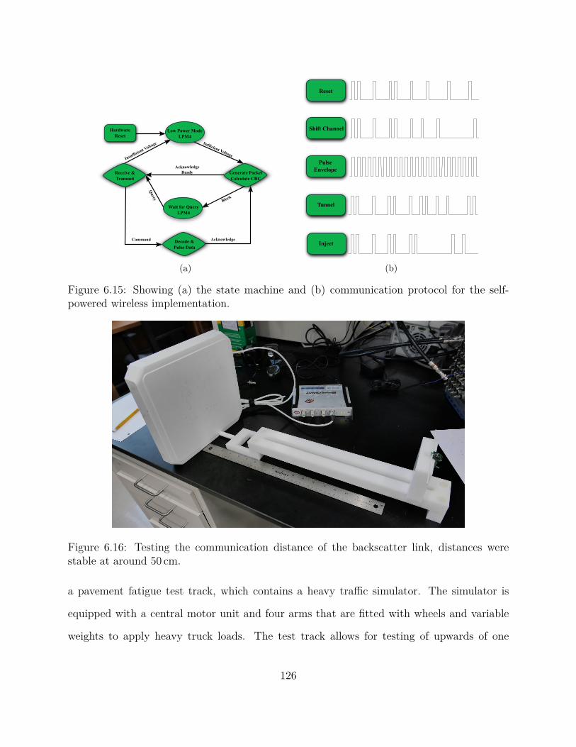
Hardware
Reset
Wait for Query
LPM4
Decode &
Pulse Data
Sufficient VoltageInsuffic
ient Volta
ge
Block
Query
Command Acknowledge
Acknowledge
ReadyReceive &
Transmit
Low Power Mode
LPM4
Generate Packet
Calculate CRC
(a)
Reset
Shift Channel
Tunnel
Inject
Pulse
Envelope
(b)
Figure 6.15: Showing (a) the state machine and (b) communication protocol for the self-powered wireless implementation.
Figure 6.16: Testing the communication distance of the backscatter link, distances werestable at around 50 cm.
a pavement fatigue test track, which contains a heavy traffic simulator. The simulator is
equipped with a central motor unit and four arms that are fitted with wheels and variable
weights to apply heavy truck loads. The test track allows for testing of upwards of one
126

Figure 6.17: The BioRePavation test facility, coordinated by IFSTTAR, in Nantes, France.
million loading cycles in a single month.
Unfortunately, once deployed under the asphalt pavement, the self-powered wireless inter-
face failed to establish a communication link. The failure was either due to the change in
impedance of the backscattering center frequency (which was not adjustable using equipment
available at the time), or the attenuation of the asphalt pavement was too great. Although
a more extensive examination of the failure would have been useful, it was not pursued by
this author since that topic alone would generate sufficient work for a dissertation. Since last
explored in the context of interfacing with the PFG sensor, other researchers have reported
improvements that could make this approach viable [110, 111, 112, 113], and the topic of
self-powered sensor utilizing backscatter remains an open research topic.
Additional data from the Nantes deployment is not available for public dissemination yet,
but laboratory testing [114] of a similar condition is presented here. The objective is to
recreate the damage index variation curves using only the cumulative information tracked
127
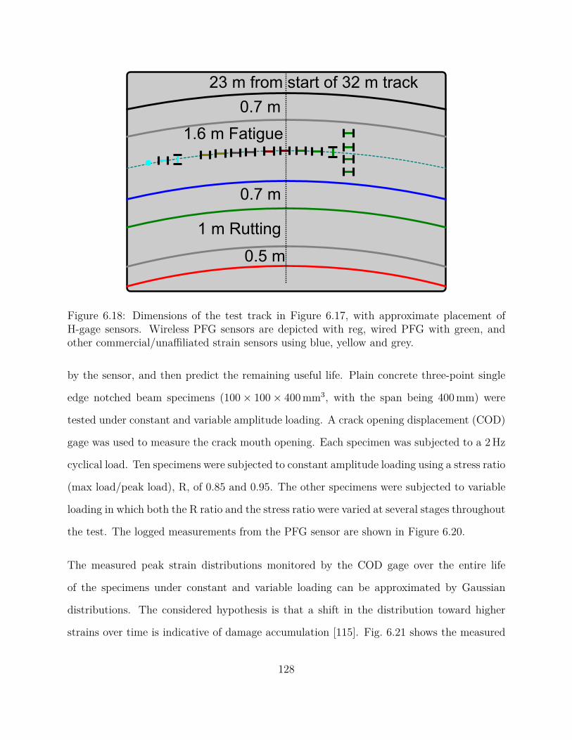
23 m from start of 32 m track
0.5 m 1 m Rutting
0.7 m
1.6 m Fatigue
0.7 m
Figure 6.18: Dimensions of the test track in Figure 6.17, with approximate placement ofH-gage sensors. Wireless PFG sensors are depicted with reg, wired PFG with green, andother commercial/unaffiliated strain sensors using blue, yellow and grey.
by the sensor, and then predict the remaining useful life. Plain concrete three-point single
edge notched beam specimens (100 × 100 × 400 mm3, with the span being 400 mm) were
tested under constant and variable amplitude loading. A crack opening displacement (COD)
gage was used to measure the crack mouth opening. Each specimen was subjected to a 2 Hz
cyclical load. Ten specimens were subjected to constant amplitude loading using a stress ratio
(max load/peak load), R, of 0.85 and 0.95. The other specimens were subjected to variable
loading in which both the R ratio and the stress ratio were varied at several stages throughout
the test. The logged measurements from the PFG sensor are shown in Figure 6.20.
The measured peak strain distributions monitored by the COD gage over the entire life
of the specimens under constant and variable loading can be approximated by Gaussian
distributions. The considered hypothesis is that a shift in the distribution toward higher
strains over time is indicative of damage accumulation [115]. Fig. 6.21 shows the measured
128

Figure 6.19: The H-gage sensors being placed for installation before being covered by virginaggregate and petroleum bitumen asphalt pavement.
strain cumulative distribution function (CDF) from the sensor at different life stages of the
beam. The normalized probability distribution function reconstructed from the measured
CDF (Fig. 6.22) clearly illustrate the shifts in the mean toward higher values, which can be
correlated to damage. Additional analysis is relegated to the realm of civil engineering and
though omitted from this dissertation, is available in literature [97, 100, 79].
6.3 Quasi-Self-Powered Wireless
Structural health monitoring (SHM) is the process used to identify potential damage or
impending failure in civil infrastructure. While SHM technique include legacy approaches
like routine/manual inspection of different structural components, recent developments in
the SHM field have investigated the capabilities and advantages of wireless sensor networks
129

Load Cycles (x1000)0 20 40 60 80 100 120 140
0
0.5
1
1.5
2
2.5
3
3.5
4
4.5
5
Cu
mu
lative
In
jectio
n (
V)
70075080090010001100120012501350
Strain (με)
Figure 6.20: The logged data from the PFG sensors (with supply voltage 5 V) is roughlylinear with respect to the number of loading cycles.
Load Cycles
Cum
mula
tive D
istr
ibution (
Voltage)
Deformation/Strain Amplitude (µε)
140 k
120 k
100 k
90 k
80 k
70 k10 k
60 k
50 k
40 k
30 k
20 k
1000900800700600 1100 1200 1300 14000
1
2
3
4
5
Figure 6.21: Cumulative distribution of voltages from data in Figure 6.20.
(WSNs) for sensing and data collection [116, 117, 118]. However, nearly all of the viable
sensing platforms use an external power source, such as: mains power, batteries, or solar [119,
120, 121, 122]. The need for explicit wiring significantly hampers the coverage of the sensors
on a large infrastructure like a multi-span bridge. Also, periodic replacement of batteries
130

Strain Level (με)
No
rma
lize
d D
en
sity
10,000 Cycles 140,000 Cycles1.0
0.8
0.6
0.4
0.2
0
-0.2600 700 800 900 1000 1100 1200 1300 1400
Figure 6.22: Showing the distribution of PFG data, as the sensor logs more loading cycles,the plots shift higher on the x-axis if the test material fatigues.
can restrict the number of deployable sensors if the batteries do not match or exceed the
structure’s lifespan. While energy-harvesting solutions such as solar can be beneficial, they
are not always an option in sensors that require complete encapsulation or placement away
from direct sunlight [123, 124, 125, 126, 127]. Also, many of these sensors utilize polling
methods and sleep-wake cycles to reduce their energy usage [128, 129, 130] which could
lead to data loss when the objective is to accurately record the impact of rare events like
earthquakes or localized buckling.
Several researchers have developed concepts for SHM, but only a few have been able to deploy
these devices on real life structures under actual loading and environmental conditions. One
example or real-world deployment is reported in [131], where a proof of concept wireless
sensing unit is shown to acquire data and transmit directly to a single base station with no
intermediate hops. However, the proposed method does limit the placement of sensor nodes
and has not been shown to scale beyond single devices. A wireless sensor network with
multiple hops, “Wisden,” has been demonstrated to accurately determine the dominant
modal frequencies of a structure, although this also has limitations on the scalability and
131
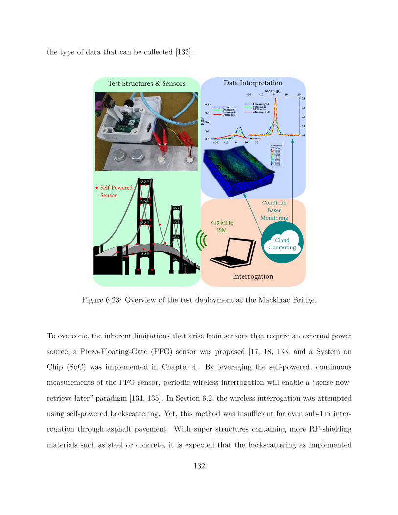
the type of data that can be collected [132].
Self-Powered
Sensor
915 MHz
ISM
Test Structures & Sensors
Interrogation
Condition
Based
Monitoring
Data Interpretation
Cloud
Computing
IntactDamage 1Damage 2Damage 3
0.3
0.2
0.1
0.0−20 −10 0 10 20
PD
F
0.4
0.4
0.3
0.2
0.1
0.0
−20 −10 0 10 20Mean (μ)
Undamaged50% Loose90% LooseMissing Bolt
E. Max. Principal(Avg: 75%)
+2.810e-04+2.576e-04+2.341e-04+2.107e-04+1.873e-04+1.639e-04+1.405e-04+1.171e-04+9.366e-05+7.024e-05+4.683e-05+2.341e-05+3.592e-12
Figure 6.23: Overview of the test deployment at the Mackinac Bridge.
To overcome the inherent limitations that arise from sensors that require an external power
source, a Piezo-Floating-Gate (PFG) sensor was proposed [17, 18, 133] and a System on
Chip (SoC) was implemented in Chapter 4. By leveraging the self-powered, continuous
measurements of the PFG sensor, periodic wireless interrogation will enable a “sense-now-
retrieve-later” paradigm [134, 135]. In Section 6.2, the wireless interrogation was attempted
using self-powered backscattering. Yet, this method was insufficient for even sub-1 m inter-
rogation through asphalt pavement. With super structures containing more RF-shielding
materials such as steel or concrete, it is expected that the backscattering as implemented
132

in Section 6.2 would also fail, thus in this section the wireless interface is replaced with an
active transmission. The combination of the self-powered sensor with the active RF interface
yields a quasi-self-powered wireless sensor. This platform is tested on a bridge health moni-
toring application, with a deployment on one of the longest suspension bridges in the world,
the Mackinac Bridge in northern Michigan. Testing at this site was conducted for over 18
months and counting. The basic framework of sensing that was used in the application is
presented in Figure 6.23, which shows how self-powered sensors could be attached to the
Mackinac Bridge on the left. Periodic interrogation would be done using the 915 MHz ISM
frequency and data is logged on a general purpose computer for further analysis. Detailed
data interpretation that infers the health of the structure is not detailed in this dissertation
as it is beyond the scope of research, and readers should not assume that any presented
findings are indicative of the current condition of the Mackinac Bridge.
6.3.1 System Design for Deployment
The Mackinac Bridge is the gateway to the north that connects the upper and lower penin-
sulas of Michigan in the United State of America. At the time of it’s construction in the
1950’s it was heralded as one of the greatest engineering structures in the world, and claimed
the title of longest suspension bridge; decades later it remains the longest suspension bridge
in the western hemisphere with a total structure length of 3038 m(26 372 ft) and width of
20.9 m(68.6 ft) and peak tower height of 168 m(552 ft). Its scale provides an excellent venue
for testing our bridge sensing platform, especially consider the harsh climate that the sensors
will need to endure, with months of sub-zero weather anticipated.
In earlier deployments of the PFG for pavement monitoring applications, the feasibility
of using backscatter RF for data retrieval was demonstrated [76, 80, 81]. However, these
methods do not work well in the presence of RF attenuating materials, as was the case in
133

80 μm
140 μ
m
1.5 mm x 1.5 mm
a
bcd
e
f
g
Mfg
Figure 6.24: (a) Digital Control, (b) Oscillator, (c) Charge Pumps, (d) Protection, Rectifier,and Time Dilation, (e) Pulse ADC, (f) PFG Core, (g) Voltage Reference and InjectionControl. Zoomed inset shows a single channel of the PFG, with the floating-gate highlightedin red.
Section 6.2. It is assumed that they would also fail in communicating on the dense steel
structure of the bridge, especially considering that the placement of the sensors from the
road surface would be greater than the open-air communication distances verified in the
laboratory. Therefore, the self-powered PFG sensor is coupled to an active Radio Frequency
(RF) communication link leading to a quasi-self-powered platform [134, 135, 136].
Initial Prototypes
Before the 2016–2017 winter season, an initial prototype was deployed on the bridge to get a
rough indication of the environmental conditions that a deployed sensor would be subjected
to and also used this opportunity to ensure that an appropriate procedure for mounting the
piezoelectric transducers to the steel super structure was in place, such that it would survive
temperatures below −40 C [135].
134

(a)
(b)
Figure 6.25: The first prototype (a) with lid on, a U.S. quarter is shown for scale, and thesize of the PFG module and PZT transducer are shown, (b) a look inside the first prototypethat implements the RF communication.
The initial prototype consisted of a Texas Instruments (TI) CC1310 Launchpad connected
to three PFG sensors using a custom PCB as an adaptor. In previous cases, the PCB were
designed in Eagle [137], but due to licensing restrictions, further PCB designs were done in
135

KiCAD. For protection against the elements, the prototype was placed in a plastic enclosure
of dimensions 16 cm×9 cm×4 cm. Each PFG sensor was connected to one of PZT1, PZT2,
or PZT3 using the C8101.41.03 cable, with the three cables passing through a single cable
gland. To power the Launchpad, four AA batteries were used to provide approximately
10 Ah of 3 V supply. The CC1310 from TI is a commercial off-the-shelf RF microcontroller
(MCU) that enables wireless communication in the 915 MHz Industrial, Scientific and Medi-
cal radio band (ISM band), while simultaneously offering capabilities typical of MCUs, such
as programmable general purpose input/output pins (GPIO), clock timing with ms preci-
sion, and user-programmable firmware. In this initial prototype, the GPIO are used to give
a rising edge to pre-determined pins of the PFG to send commands such as: increment se-
lected channel, reset all channels, program current channel, enable readout, and reset PFG
state machine. By using a second TI CC1310 Launchpad that is connected to a PC, one
can send specific wireless commands that are encoded per TI’s sub-GHz specifications to
control individual PFG sensors within each prototype, and to log the output data of the
sensors on the PC for further analysis. On the RF side, the CC1310 was configured for an
average active supply current draw of 12 mA with wireless communication sensitivity below
−110 dB m. Estimates using TI datasheets suggest that this setup could yield wireless ranges
in excess of 1 km even with a low efficiency PCB antenna.
Images of the initial prototype are shown in Figure 6.25 with the actual installation cite
omitted here, but available in [134]. At the time of installation in September, the three PFG
sensors had readings of 5468 Hz, 5335 Hz, and 5202 Hz. After two months of deployment,
the collected readings in November were 1661 Hz, <800 Hz, and 1034 Hz for the three PFG
sensors, respectively. Although specific infrastructural health based on these data points
cannot be commented on, it does demonstrate that the platform was continuously logging
data even without external power, and that the chosen active RF solution was sufficient
136

in enabling transmissions that allows interrogation of the sensors while simply driving over
the bridge with a laptop and Launchpad at the Mackinac Bridge speed limit of 45 mph
(72 km h−1).
Unfortunately, the first prototype did not survive the first winter season. The failure mode
was the ingress of moisture from a gap in the single cable gland (which was filled with silicone
sealant) that built up inside the enclosure box. The moisture caused a short of the internal
electronics and the batteries were found to have died. It is hypothesized that this was not an
issue during the two months of deployment between September and November since sub-zero
temperatures were less common. Once the snow and ice accumulated in the winter, it would
also increase the chance of water making its way into the enclosure. The PFG sensors and
PZT transducers were operational during evaluation of the prototype after it was recovered
from the bridge and taken back to the laboratory.
Second Prototype
Taking into account the lessons learned from the initial prototype, an improved version was
designed. The improved sensor assembly is shown as Figure 6.26a and the weatherproof
enclosure is presented in Figure 6.26b. A custom PCB that has a built-in PCB antenna
connected to TI’s CC1310 RF MCU was designed to minimize cost. As in the initial pro-
totype, this component enables the active wireless communication and interfaces with up to
three PFG sensors per box. Each PFG is soldered onto an individual daughterboard module
that can be easily swapped in or out on the RF motherboard via flexible flat cables. This
capability allows for rapid replacement of PFG sensors if a change in the injection rate,
diagnosis of a failure, or resetting the floating gate memory (though possible through the
wireless communication, we removed this option to prevent malicious tampering of data at
this stage) is required.
137

f
e
c
a
d
b
(a) (b)
(c)
Figure 6.26: (a) Custom built PCB that has a. ultra-low-power sleep mode, b. interfaceto hot-swappable PFG sensors, c. buck converter, d. RF MCU, e. antenna, and f. PFGsensor modules. (b) Shows an assembled box, sans sensor modules and (c) has images of theMackinac Bridge and the installation on steel support beams.
The three cables were replaced with a single six conductor cable (General Cables, C3029.41.86)
which uses 24 AWG wires, a flouropolymer jacket insulation that is rated for operation be-
tween −40 C to 150 C and has a reduced capacitance of 13 pF/ft between conductors and
138
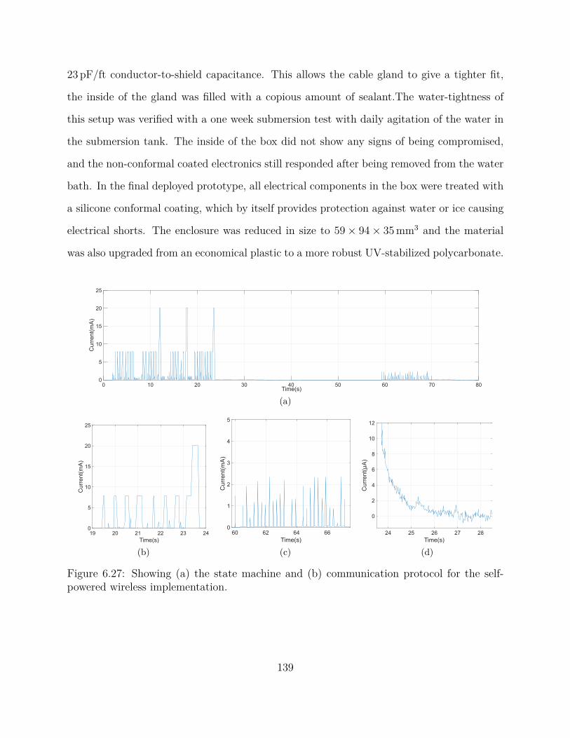
23 pF/ft conductor-to-shield capacitance. This allows the cable gland to give a tighter fit,
the inside of the gland was filled with a copious amount of sealant.The water-tightness of
this setup was verified with a one week submersion test with daily agitation of the water in
the submersion tank. The inside of the box did not show any signs of being compromised,
and the non-conformal coated electronics still responded after being removed from the water
bath. In the final deployed prototype, all electrical components in the box were treated with
a silicone conformal coating, which by itself provides protection against water or ice causing
electrical shorts. The enclosure was reduced in size to 59 × 94 × 35 mm3 and the material
was also upgraded from an economical plastic to a more robust UV-stabilized polycarbonate.
0 10 20 30 40 50 60 70 80Time(s)
0
5
10
15
20
25
Current(mA)
(a)
19 20 21 22 23 24
Time(s)
0
5
10
15
20
25
Current(mA)
(b)
60 62 64 66
Time(s)
0
1
2
3
4
5
Current(mA)
(c)
24 25 26 27 28
Time(s)
0
2
4
6
8
10
12
Current(µA)
(d)
Figure 6.27: Showing (a) the state machine and (b) communication protocol for the self-powered wireless implementation.
139
The RF motherboard also includes a buck converter to extract more energy from the batteries
before the system stops responding due to low supply voltage. Additionally, a nano-power
timer (TI TPL5111) disconnected all electronics from the battery by turning off a load
switch. This user-configurable timer was set for 5 minutes, therefore the prototype would
be unresponsive for 5 minutes at a time, but would only lose a miniscule amount of supply
current to leakage, measured to be less than 50 nA (Figure 6.27d). On the initial startup, the
RF MCU is programmed to go into a “search” mode where it will listen for an interrogator
(i.e. an operator that has a similar RF board connected to their PC and is asking for
data) with supply current measured in Figure 6.27c. Only if an interrogator is detected will
the prototype transmit the PFG sensor data. The transmission was repeated three times to
ensure delivery and the supply current of a single transmission cycle is shown in Figure 6.27b.
The “search” before transmit is done since the energy cost of a transmission is much larger
than receiving, in particular the CC1310 was configured to listen for an interrogator for 6 s
at a time with an average supply current of 225 µA while a transmission can take as long as
13.5 s with an order of magnitude larger supply current of 2.5 mA. Based on these supply
currents, one can estimate typical supply currents of:
Request =Ionton + Isearchtsearch + Iofftoff
ton + tsearch + toff
=2.5 m · 13.5 + 225µ · 6 + 50 n · 300
13.5 + 6 + 300< 110µA
No request =Isearchtsearch + Iofftoff
tsearch + toff
=225µ · 6 + 50 n · 300
6 + 300< 5µA
140

If data are collected from these sensor boxes twice a day (that is, 1% of the time), and they
use a ½ AA battery with 1.2 Ah of capacity, then it would remain operational for:
1.2 Ah ÷ (0.99 · 5µ + 0.01 · 110µ) A ·(
1 yr
8766 h
)
≈ 23.5 years.
In a more traditional sensing platform, the MCU would need to periodically poll the sensors
to collect sufficiently meaningful data, which would prevent them from operating at the nA
range that this prototype does. Moreover, in such polling methods, the collected data would
necessarily be missing spurious parts of the history since they are not doing continuous data
collection [80]. It should be noted that many conventional battery formulations would fail to
last decades in an actual deployment, lead-acid might decay 5% per month, and the latest
alkaline batteries have 2% self-discharge annually. Lithium-ion tends to do even worse, with
2% lose per month. And these rates are further exacerbated in real-world deployments that
endure thermal cycling [138]. In the proposed application, a lithium thionyl chloride battery
from Tadiran is utilized, the supplier has over 40 years of experience, and has documented
customers that have deployed this battery chemistry successfully for over 25 years [139].
Accelerated testing with thermal cycling was done in-lab to verify the manufacturer’s claims
and a TL-4902 was modeled to last upwards of 50 years. Using this battery pushes the
limitation of the sensing platform’s lifespan towards surface mount components such as
capacitors, which are only guaranteed for 20 years of operation. Some of these operational
limitations can be designed around by inspecting Monte Carlo analysis and defining a safe
margin of degradation.
141
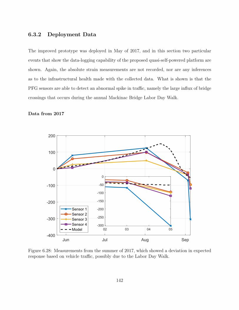
6.3.2 Deployment Data
The improved prototype was deployed in May of 2017, and in this section two particular
events that show the data-logging capability of the proposed quasi-self-powered platform are
shown. Again, the absolute strain measurements are not recorded, nor are any inferences
as to the infrastructural health made with the collected data. What is shown is that the
PFG sensors are able to detect an abnormal spike in traffic, namely the large influx of bridge
crossings that occurs during the annual Mackinac Bridge Labor Day Walk.
Data from 2017
Jun Jul Aug Sep-400
-300
-200
-100
0
100
200
Sensor 1
Sensor 2
Sensor 3
Sensor 4
Model 02 03 04 05-300
-250
-200
-150
-100
-50
0
Figure 6.28: Measurements from the summer of 2017, which showed a deviation in expectedresponse based on vehicle traffic, possibly due to the Labor Day Walk.
142

The data collected between May 25th and September 5th of 2017 are presented in Figure 6.28
after having the corrective factors from Chapter 4 applied [135]. Sensors 1 through 3 are
at the same installation site and show the same trend in data logging, with some difference
in peak frequency as well as injection rate due to fabrication mismatch. Sensor 4 was on
a different installation site, but had a similar configuration in terms of PZT size and PFG
tuning parameters. The sparse data collection appears to follow the trend that we expected
based on the PFG characterizations from in-lab testing [19, 72, 73, 140, 141] and the traffic
statistics of the Mackinac Bridge provided by the Mackinac Bridge Authority. The trend line
is shown as the dashed black. The inset of Figure 6.28 shows the data collected before and
after the Mackinac Bridge Labor Day Walk (on Sep. 4th), which drew a crowd of over 25,000
people, much greater than usual traffic on the bridge. It shows that during the event the
sensors logged a much larger amount of data than it had in the days before. The deviation
from the model trace, which is based on monthly traffic statistics, highlights the extra strain
that the Labor Day Walk placed on the sensors. Note that measurements are shown in a unit-
less, corrective-factor-applied frequency output of a single channel from each PFG sensor,
from which a layperson may have trouble extracting any meaningful information. It has
been previously demonstrated that similar data can infer the structural damage progression
in steel frames, girders, and plates [142].
Data from 2018
After leaving the prototypes deployed on the bridge for the 2017–2018 winter season, they
were still responding when returning to the bridge in the spring of 2018. Upon opening the
boxes for inspection, it was found that none of the four units showed signs of water ingress
or other hardware failures. The battery levels were also as expected based on the calculated
operational lifespan of 23.5 yrs per ½ AA battery. The sensors remained operational through
143

Aug 29 Aug 30 Aug 31 Sep 01 Sep 02 Sep 03 Sep 04
2018
0.8
1
1.2
1.4
1.6
1.8
PF
G D
ata
(V
)
Box 12
Sensor 1
Sensor 2
Sensor 3
Trend
Figure 6.29: PFG with accelerated injection rates were used to focus on the single day eventof the Mackinac Labor Day Walk of 2018.
the summer season as well. Before the annual Mackinac Bridge Labor Day Walk for 2018, the
PFG sensors in Box 12 were swapped out with ones that would log data more quickly (using
a smaller external tuning resistor on the reference voltage generator) to see if the findings
from 2017 could be replicated [143]. In this section, the pulse encoder output frequency
was translated into an equivalent stored floating gate charge, which is denoted as the PFG
Data in volts. The resulting data plots are given in Figure 6.29, and show that the data
logging before Labor Day (which was on September 3, 2018) was slower than during the
event. Sensor 2 was consistently logging data, regardless of the traffic levels, which might
be expected due to the placement of that PZT since it could be tracking the sway of the
bridge from winds, or aspects of the bridge health that wouldn’t be affected by a change
in traffic patterns. According to the Mackinac Bridge Authority, it is typical for winds to
144

cause horizontal sways of 35 ft, and if the placement of the PZT is correct, Sensor 2 could
be logging such horizontal strains instead of the vertical strains that would be generated
by passing traffic. Sensors 1 and 3 showed a large change cumulative history of strains
experienced by their PZTs. More in-depth discussion of the validity of the gathered data
with the self-powered sensing platform are reported in literature [144, 75, 145, 146, 140, 97].
6.3.3 Other Deployments
Figure 6.30: Sensor boxes on a wind turbine blade that was tested in collaboration withNREL.
The quasi-self-powered sensor box was also tested on a wind turbine blade [147], as shown
in Figure 6.30, in collaboration with the National Renewable Energy Laboratory (NREL)
and General Electric. Measurement results are not available for disclosure, but the wireless
sensor boxes were able to perform as expected in this deployment as well. Another on-going
145
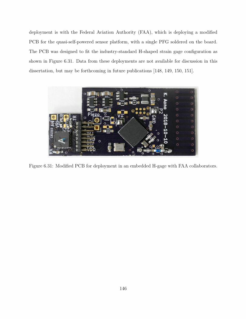
deployment is with the Federal Aviation Authority (FAA), which is deploying a modified
PCB for the quasi-self-powered sensor platform, with a single PFG soldered on the board.
The PCB was designed to fit the industry-standard H-shaped strain gage configuration as
shown in Figure 6.31. Data from these deployments are not available for discussion in this
dissertation, but may be forthcoming in future publications [148, 149, 150, 151].
Figure 6.31: Modified PCB for deployment in an embedded H-gage with FAA collaborators.
146

Chapter 7
Closing Remarks
With this chapter, I conclude a body of work that encompasses the efforts devoted towards
a Doctor of Philosophy degree in engineering. The primary interest that drove me to pursue
advanced degrees in electrical and computer engineering was: taking inspiration from systems
and physical phenomenon that occur in nature and bending them to our will.
Forming the basis of motivation for the jump resonance filter of Chapter 3 was that cochlea
exhibit similar nonlinearities [152, 40, 153], yet it was common to use symmetric, linear
filters when building filter banks for auditory front-ends [32, 154, 155]. At the time this
research was taking place over six years ago, the digital tools available to a single researcher
would have been preventative in my search for answering the question of whether or not
including such non-ideal features would aid in applications such as speaker recognition.
Recent literature continues to investigate similarly using jump resonance features, and with
the explosive growth in parallel computing capabilities it can be achieved in the digital
domain [156, 157, 158, 159]. Yet, because the reported jump resonance filters exploit physical
phenomenon that are inherently preset in analog filters, the energy efficiency remains orders
of magnitude greater than their digital brethren.
147

In another thread of this story, I dove into the world of Piezoelectric-Floating-Gate (PFG)
sensors. During the jump resonance investigation, having a means for data-logging of the
past experienced input stimuli was something that interested me. My thought was that
using the history of past events, I could adaptively program the filter biases to adjust the
“hearing” of the silicon cochlea to automatically increase its performance as it “ages”. Since
the jump resonance filter already used floating-gates to tune the biasing of the transconduc-
tance amplifiers within the biquad filter [160, 161] it was only natural for me to extend my
field of research to the PFG sensors developed by my advisor.
A note to readers, the work in Chapter 3 and Sections 6.1 & 6.2 mostly took place while I
was at Michigan State University. The work in Sections 6.3 & Chapter 5 were conducted
primarily at Washington University in St. Louis, with Chapter 4 overlapping between both
universities.
7.1 Findings and Conclusion
• ♠♣ s♦♥♥ ②strss ♥ ♦♥ ♦ An oft unsought ar-
tifact that presents in certain current-mode filter configurations when attempting to
attain high quality factor filtering, jump resonance, was probed for useful work. The
sharp filter edges in the frequency domain, and the non-symmetric nature of the hys-
teresis was wielded to generate a features set that was more discriminating than stan-
dard linear filters. With respect to probability of detection on a test set of 20 speakers,
a linear filter implemented in hardware had 90.94%, whereas the jump resonance chip
that was fabricated achieved 98.75%.
• rtr③t♦♥ ♦ ♥r ♥t♦r A System-on-Chip (SoC) imple-
mentation of the linear injector reported by Dr. Huang [20] was tested under various
148

conditions. After considering additional buffering distortions and a lower supply volt-
age of 1.8 V versus the originally reported 4 V, certain aspects such as the linearity
(effective number of bits 12.979) and repeatable nature of the linear injection (less
than 1% error) were validated. In the course of a more in-depth testing that leveraged
new laboratory assets such as a thermally-controlled environment chamber, several
shortcomings were uncovered. For example, the digital readout circuitry may deviate
as much as 8% with a 1 C change in ambient temperature, or the output buffers may
not correctly reflect the charge stored on the floating-gate.
• r♥sr t♦ Prt ♦r ②rP②s ②st♠ The Piezoelectric-
Floating-Gate (PFG) sensor was taken out of the laboratory setting and deployed to
real world test cases. This involved fabrication of a SoC with all necessary voltage ref-
erences and interface circuitry for programming, sensing, and reading. Another major
thrust of this effort was investigating wireless interrogation techniques that would en-
able the PFG sensor to be embedded within structures. Early efforts centered around
deployments that could tolerate having wires exposed or those that could allow for
backscatter power and communication. The use of cabling limited the sites that could
be targeted, and the self-powered backscattering technique proved difficult to mas-
ter without significant resource investment. To circumvent these limitations, quasi-
self-powered and hybrid-powered wireless methods were proposed and implemented in
practice. These methods have demonstrated the usefulness of the PFG’s self-powered
sensing in structural health monitoring applications.
Although not all of the work can be published, I would like to acknowledge the many
partners in deployment testing: Mackinac Bridge Authority (MBA), Federal Highway
Administration (FHWA), Federal Aviation Administration (FAA), Air Force Research
Lab (AFRL) Materials and Manufacturing Directorate, National Wind Technology
149

Center (NWTC), National Renewable Energy Laboratory (NREL), Michigan Depart-
ment of Transportation (MDOT), Florida Department of Transportation (FDOT),French
Institute of Science and Technology for Transport, Spatial Planning, Development and
Networks (IFSTTAR), Michigan State University (MSU), University of Southern Cal-
ifornia (USC), University of Nevada-Reno (UNR), University of Missouri (MU), Uni-
versity of Nottingham, and University of Palermo.
• ♦ ♥ ♥♣t ♦ ♥r ♥t♦r In the case of struc-
tural health monitoring with the PFG sensor, the acceleration of structures causes
micro strains across the surface of the material. Via the piezoelectric transducer, these
strains become voltages that are interfaced with our PFG SoC. The electric field po-
tential is a function of the input strain level, but not necessarily the frequency of the
strains. When data-logging sensor data, there is an apparent desire for having fre-
quency data about input stimuli since it would allow better selectivity for monitoring
of specific events. A modification to the core of the linear feedback injector of the PFG
was proposed, using similar filter techniques as in the jump resonance chip. Although a
low-pass filter response was expected, the measurements from a fabricated chip shows
a more bandpass like response. In many deployments, a bandpass filter would be
useful, but this modified topology will require additional study before it is ready for
deployments. Another modification was done to the input stage, which now allows for
a capacitively coupled input directly to the floating-gate node. It was verified that this
method offers a means for data-logging of input stimuli smaller than the ≈6 V required
for the traditional PFG. Using a differential structure, it would be possible to log and
detect stimuli in the milli-volt scale.
150

7.2 Future Direction
• ♦♣♥ ♦r ♦st ②rP②s ②st♠ To overcome
some of the limitations in the current implementation, several tasks can need to be
undertaken. First, the entire design should be migrated away from the ON Semicon-
ductor 0.5 µm process to a more readily available process such as the 180 nm process
by TSMC. This transition would enable a more rapid cadence of iterations to test and
verify new ideas. Second, in the interest of time, design choices like having a single-
slope ADC (has non-monotonic output), using a PTAT current source (more than 5%
deviation per 1 C), and having simple amplifiers (cannot drive rail-to-rail) were made
during the prototyping phase. Now that the prototypes have demonstrated the capa-
bilities of the PFG concept, the circuit implementations of certain blocks should be
reevaluated. A move to 180 nm could also enable the placement of RF components
onto the SoC, which would vastly decrease the cost of deployment and allow greater
flexibility in applications such as backscattering.
Aside from the straightforward changes to the PFG implementation, there were many
topology variations proposed in the course of this dissertation work that did not get
fully fleshed out and explored. These include variants that can: log the time of events,
have programmable level thresholds, greater injection sensitivity using diodes, daisy-
chainable SoC data banks, non-overlapping data-logging (i.e. channel 1 stops recording
if channel 2 is activated), higher effective number of bits, etc.
• ①♣♦r♥ ♦♠♥s ♦r t P ②♦♥ trtr t ♦♥
t♦r♥ In Chapter 6, the PFG was deployed and testing on several civil engineering
applications, primarily with respect to structural health monitoring. This technology
151

can also be used in biomedical applications, as reported in Appendix A. Further explo-
ration of non-civil applications has been limited due to a lack of time, and because the
traditional PFG required large excitations to trigger the data-logging process, thereby
limiting applications to the legs which absorb large impact forces [162]. With the more
sensitive variant of the PFG that utilizes capacitive coupling, topics such as spinal cord
fusion, organ growth, and cranial trauma could be avenues of research.
152

References
[1] A. Hande, R. Bridgelall, and B. Zoghi, “Vibration energy harvesting for disaster assetmonitoring using active RFID tags,” Proceedings of the IEEE, vol. 98, no. 9, pp. 1620–1628, 2010.
[2] A. M. Zungeru, L.-M. Ang, S. Prabaharan, and K. P. Seng, “Radio frequency energyharvesting and management for wireless sensor networks,” Green mobile devices andnetworks: Energy optimization and scavenging techniques, pp. 341–368, 2012.
[3] H.-U. Kim, W.-H. Lee, H. R. Dias, and S. Priya, “Piezoelectric microgenerators-currentstatus and challenges,” IEEE transactions on ultrasonics, ferroelectrics, and frequencycontrol, vol. 56, no. 8, 2009.
[4] S. Roundy, P. K. Wright, and J. Rabaey, “A study of low level vibrations as a powersource for wireless sensor nodes,” Computer Communications, vol. 26, no. 11, pp.1131–1144, 2003, ubiquitous Computing.
[5] S. Dalola, M. Ferrari, V. Ferrari, M. Guizzetti, D. Marioli, and A. Taroni, “Character-ization of thermoelectric modules for powering autonomous sensors,” IEEE Transac-tions on Instrumentation and Measurement, vol. 58, no. 1, pp. 99–107, 2009.
[6] R. A. Bullen, T. Arnot, J. Lakeman, and F. Walsh, “Biofuel cells and their develop-ment,” Biosensors and Bioelectronics, vol. 21, no. 11, pp. 2015–2045, 2006.
[7] S. H. Kondapalli, Y. Alazzawi, M. Malinowski, T. Timek, and S. Chakrabartty, “Multi-access In Vivo Biotelemetry Using Sonomicrometry and M-Scan Ultrasound Imaging,”IEEE Transactions on Biomedical Engineering, vol. 65, no. 1, pp. 149–158, Jan. 2018.
[8] G. E. Moore, “Progress in digital integrated electronics,” in Proc. IEEE Int. ElectronDevices Meet. Dig. Tech Papers, 1975, pp. 11–13.
[9] L. Bolotnyy and G. Robins, “The case of multi-tag RFID systems,” in IEEE Interna-tional Conference on Wireless Algorithms, System and Applications (WASA), Chicago,U.S.A., Aug. 2007, pp. 174–186.
[10] M. Lallart, L. Garbuio, L. Petit, C. Richard, and D. Guyomar, “Double synchronizedswitch harvesting (DSSH): A new energy harvesting scheme for efficient energy ex-traction,” Ultrasonics, Ferroelectrics and Frequency Control, IEEE Transactions on,vol. 55, no. 10, pp. 2119–2130, 2008.
153

[11] L. Garbuio, M. Lallart, D. Guyomar, C. Richard, and D. Audigier, “Mechanical energyharvester with ultralow threshold rectification based on SSHI nonlinear technique,”Industrial Electronics, IEEE Transactions on, vol. 56, no. 4, pp. 1048–1056, 2009.
[12] Y. K. Ramadass and A. P. Chandrakasan, “An efficient piezoelectric energy harvestinginterface circuit using a bias-flip rectifier and shared inductor,” Solid-State Circuits,IEEE Journal of, vol. 45, no. 1, pp. 189–204, 2010.
[13] S. Xu, K. D. Ngo, T. Nishida, G.-B. Chung, and A. Sharma, “Low frequency pulsedresonant converter for energy harvesting,” Power Electronics, IEEE Transactions on,vol. 22, no. 1, pp. 63–68, 2007.
[14] R. D’hulst, T. Sterken, R. Puers, G. Deconinck, and J. Driesen, “Power processing cir-cuits for piezoelectric vibration-based energy harvesters,” Industrial Electronics, IEEETransactions on, vol. 57, no. 12, pp. 4170–4177, 2010.
[15] D. Kwon and G. A. Rincón-Mora, “A 2-m BiCMOS Rectifier-Free AC–DC PiezoelectricEnergy Harvester-Charger IC,” Biomedical Circuits and Systems, IEEE Transactionson, vol. 4, no. 6, pp. 400–409, 2010.
[16] A. Tabesh and L. G. Fréchette, “A low-power stand-alone adaptive circuit for harvest-ing energy from a piezoelectric micropower generator,” Industrial Electronics, IEEETransactions on, vol. 57, no. 3, pp. 840–849, 2010.
[17] S. Chakrabartty, “Self-powered Strain-rate Sensor,” 2010, patent No. 7757565, Issued2010.
[18] S. Chakrabartty, N. Lajnef, N. Elvin, and A. Gore, “Self-powered Sensor,” 2011, patentNo. 8056420, Issued 2011.
[19] C. Huang, N. Lajnef, and S. Chakrabartty, “Calibration and characterization of self-powered floating-gate usage monitor with single electron per second operational limit,”Circuits and Systems I: Regular Papers, IEEE Transactions on, vol. 57, no. 3, pp. 556–567, 2010.
[20] C. Huang, P. Sarkar, and S. Chakrabartty, “Rail-to-Rail, Linear Hot-Electron InjectionProgramming of Floating-Gate Voltage Bias Generators at 13-Bit Resolution,” IEEEJournal of Solid-State Circuits, vol. 46, no. 11, pp. 2685–2692, 2011. [Online].Available: https://doi.org/10.1109/JSSC.2011.2167390
[21] J. L. Douce, “A note on the evaluation of the response of a non-linear element tosinusoidal and random signals,” Proceedings of the IEE - Part C: Monographs, vol.105, no. 7, pp. 88–92, Mar. 1958.
[22] S. H. Kyong, “Jump Criteria of Nonlinear Control Systems and the Validity of Statis-tical Linearization Approximation,” The Bell System Technical Journal, vol. 48, no. 8,pp. 2529–2543, Sep. 1969.
154

[23] A. Fukuma and M. Matsubara, “Jump resonance in nonlinear feedback systems–PartI: Approximate analysis by the describing-function method,” IEEE Trans. Autom.Control, vol. 23, no. 5, pp. 891–896, Oct. 1978.
[24] L. T. Lewis, “Harmonic Analysis for Non-Linear Characteristices,” Transactions of theAmerican IEE, vol. 73, no. 1, pp. 693–700, 1954.
[25] A. R. Bergen and R. L. Franks, “Justification of the Describing Function Method,”SIAM J. on Control and Optimization, vol. 9, no. 4, pp. 568–589, 1971.
[26] C. F. Ho, “An extension to fukuma and matsubara jump resonance criterion by the useof describing functions,” Radio and Electronic Engineer, vol. 442, no. 15, pp. 562–568,1972.
[27] A. Fukuma and M. Matsubara, “Jump Resonance Criteria of Nonlinear Control Sys-tems,” IEEE Trans. Autom. Control, vol. 11, no. 4, pp. 699–706, Oct. 1966.
[28] H. Hatanaka, “The Frequency Responses and Jump-Resonance Phenomena of Non-linear Feedback Control Systems,” J. Basic Eng., vol. 85, no. 2, pp. 236–242, Jun.1969.
[29] K. Hirai and N. Sawai, “A general criterion for Jump Resonance of Nonlinear ControlSystems,” IEEE Trans. Autom. Control, vol. 23, no. 5, pp. 896–901, Oct. 1978.
[30] A. M. Hopkin and K. Ogata, “An analytic Frequency-Response Solution for a higherorder Servomechanism with a nonlinear control element,” J. Basic Eng., vol. 81, no. 1,pp. 41–45, Mar. 1959.
[31] C. D. Salthouse and R. Sarpeshkar, “Jump Resonance: A Feedback Viewpoint andAdaptive Circuit Solution for Low-Power Active Analog Filters,” IEEE Trans. CircuitsSyst., vol. 53, no. 8, pp. 1712–1725, Aug. 2006.
[32] E. A. Freeman and M. L. Devine, “Calculation and avoidance of jump resonance infeedback amplifier circuits,” Proc. IEE, vol. 115, no. 1, pp. 229–235, Jan. 1968.
[33] R. S. Moni and K. R. Rao, “Jump-Phenomenon in Active-RC Filters,” IEEE Trans.Circuits Syst., vol. 29, no. 1, pp. 54–55, Jan. 1982.
[34] J. Glass, “Acoustic Properties of Speech Sounds,” Jun. 1999, presented at WS’99,hosted by The Center for Language and Speech Processing at The John HopkinsUniversity.
[35] A. Fazel and S. Chakrabartty, “An Overview of Statistical Pattern Recognition Tech-niques for Speaker Verification,” IEEE Circuits Syst. Mag., vol. 11, no. 2, pp. 62–81,2011.
155

[36] K. Aono, S. Chakrabartty, and T. Yamasaki, “Infrasonic Scene Fingerprinting for Au-thenticating Speaker Location,” in 2017 IEEE International Conference on Acoustics,Speech and Signal Processing (ICASSP), Mar. 2017, pp. 361–365.
[37] V. Chan, S.-C. Liu, and A. van Schaik, “AER EAR: A Matched Silicon Cochlea Pairwith Address Event Representation Interface,” IEEE Trans. Circuits Syst. I, vol. 54,no. 1, pp. 48–59, Jan. 2007.
[38] R. Sarpeshkar, “Energy-efficient adaptive signal decomposition: The silicon and bio-logical cochlea,” in Circuits and Systems, 1999. ISCAS ’99. Proceedings of the 1999IEEE International Symposium On, 1999, pp. 70–73.
[39] H. N. Teodorescu, “AI Tools for Speech Analysis Applied to the Romanian Language,”in Proceedings of The 4th European Computing Conference, 2010, pp. 272–279.
[40] L. Bian, E. E. Linhardt, and M. E. Chertoff, “Cochlear hysteresis: Observation withlow-frequency modulateddistortion product otoacoustic emissions,” J. Acoust. Soc.Am., vol. 115, no. 5, pp. 2159–2172, May 2004.
[41] L. Bian and N. M. Scherrer, “Low-frequency modulation of distortion product otoa-cousticemissions in humans,” J. Acoust. Soc. Am., vol. 122, no. 3, pp. 1681–1692, Sep.2007.
[42] S. S. Lamba and R. J. Kavanagh, “Phenomenon of isolated jump resonance and itsapplications,” Proc. IEE, vol. 118, no. 8, pp. 1047–1050, Aug. 1971.
[43] R. J. Kavanagh and D. M. Sinclair, “A Novel Frequency Meter Using Jump Resonance,”IEEE Trans. Instrum. Meas., vol. 23, pp. 178–179, Jun. 1974.
[44] A. Tustin, “A method of analysing the effect of certain kinds of non-linearity in closed-cycle control systems,” Electrical Engineers - Part IIA: Automatic Regulators andServo Mechanisms, Journal of the Institution of, vol. 94, no. 1, pp. 152–160, May1947.
[45] J. P. Campbell, “Testing with the YOHO CD-ROM voice verification corpus,” inAcoustics, Speech, and Signal Processing, 1995. ICASSP-95., 1995 International Con-ference On, vol. 1, May 1995, pp. 341–344.
[46] W. M. Campbell, K. T. Assaleh, and C. C. Broun, “Speaker recognition with polyno-mial classifiers,” IEEE Trans. Speech Audio Process., vol. 10, no. 4, pp. 205–212, May2002.
[47] A. Gore and S. Chakrabartty, “Min-Max Optimization Framework for Designing Sig-maDelta Learners: Theory and Hardware,” IEEE Trans. Circuits Syst. I, no. 3, pp.604–617, 2010.
156

[48] Ahana Gangopadhyay, Kenji Aono, Darshit Mehta, and Shantanu Chakrabartty, “ACoupled Network of Growth Transform Neurons for Spike-Encoded Auditory FeatureExtraction,” bioRxiv, Apr. 2018.
[49] B. Gold and N. Morgan, Speech and Audio Signal Processing. New York, New York:John Wiley and Sons, 2000.
[50] R. Auckenthaler, M. Carey, and H. Lloyd-Thomas, “Score normalization for text-independent speaker verification system,” Digital Signal Processing, vol. 10, no. 1,2000.
[51] Y. Gu and T. Thomas, “A text-independent speaker verification system using supportvector machines classifier,” in Proc. Eur. Conf. Speaker Communication and Technol-ogy (Eurospeech’01), Aalborg, Denmark, Sep. 2001, pp. 1765–1769.
[52] S. Chakrabartty and G. Cauwenberghs, “Gini-Support Vector Machine: QuadraticEntropy Based Multi-class Probability Regression,” Journal of Machine Learning Re-search, pp. 813–839, Apr. 2007.
[53] K. Aono, R. K. Shaga, and S. Chakrabartty, “Exploiting jump-resonance hysteresisin silicon cochlea for formant trajectory encoding,” in 2012 IEEE 55th InternationalMidwest Symposium on Circuits and Systems (MWSCAS), Aug. 2012, pp. 85–88.
[54] K. Aono, “Extracting Speaker Features from Sub-Vocal Speech Using Jump ResonanceFiltering,” Nov. 2013.
[55] Kenji Aono, “Extracting Speaker Features from Sub-Vocal Speech Using Jump Reso-nance Filtering,” in Michigan Space Grant Consortium, Annual Fall Conference, Uni-versity of Michigan, Ann Arbor, MI, Nov. 2013, pp. 1–30.
[56] ——, “Jump Resonance Filtering for Biometrics via Electromyography in Sub-VocalSpeech,” in Michigan Space Grant Consortium, Aug. 2013, pp. 1–5.
[57] ——, “EMG-based Speech Filtering & Classifier,” in MSGC Annual Conference.Michigan Space Grant Consortium, Aug. 2014, pp. 1–4.
[58] D. C. Guterman, I. H. Rimawi, T.-L. Chiu, R. D. Halvorson, and D. J. McElroy,“An Electrically Alterable Nonvolatile Memory Cell Using a Floating-Gate Structure,”IEEE Transactions on Electron Devices, vol. ED-26, no. 4, pp. 576–586, 1979.
[59] L. R. Carley, “Trimming Analog Circuits Using Floating-Gate Analog MOS Memory,”IEEE Journal of Solid-State Circuits, vol. 24, no. 6, pp. 1569–1575, Dec. 1989.
[60] K. Yang and A. G. Andreou, “A Multiple Input Differential Amplifier Based on ChargeSharing on a Floating-Gate MOSFET,” Analog Integrated Circuits and Signal Process-ing, vol. 6, pp. 197–208, 1994.
157

[61] S. L. Miller, “Ionization Rates for Holes and Electrons in Silicon,” Physical Review,vol. 105, no. 4, pp. 1246–1249, Feb. 1957.
[62] M. Lenzilinger and E. H. Snow, “Fowler-Nordheim Tunneling into Thermally GrownSiO2,” J. Applied Physics, vol. 40, no. 1, pp. 278–283, Jan. 1969.
[63] L. Zhou, K. Aono, and S. Chakrabartty, “Gaussian Process Regression for Improv-ing the Performance of Self-powered Time-of-Occurrence Sensors,” in 2018 IEEE 61stInternational Midwest Symposium on Circuits and Systems (MWSCAS), Aug. 2018.
[64] D. Mehta, L. Zhou, K. Aono, and S. Chakrabartty, “Self-powered Sensing and Time-Stamping of Tampering Events,” in 2018 IEEE 61st International Midwest Symposiumon Circuits and Systems (MWSCAS), Aug. 2018.
[65] L. Zhou and S. Chakrabartty, “Linearization of CMOS Hot-Electron Injectors forSelf-Powered Monitoring of Biomechanical Strain Variations,” IEEE Transactions onBiomedical Circuits and Systems, 2016.
[66] ——, “Self-powered sensing and time-stamping of rare events using CMOS fowler-nordheim tunneling timers,” in Circuits and Systems (ISCAS), 2016 IEEE Interna-tional Symposium On. IEEE, 2016, pp. 2839–2842.
[67] ——, “Self-Powered Timekeeping and Synchronization Using Fowler–NordheimTunneling-Based Floating-Gate Integrators,” IEEE Transactions on Electron Devices,vol. 64, no. 3, pp. 1254–1260, 2017.
[68] Liang Zhou, Kenji Aono, and Shantanu Chakrabartty, “Tamper SensitiveAuthentication of Passive IoT Devices Using Self-Powered CMOS Timers,” inTECHCON. Austin, TX: SRC, 2018. [Online]. Available: https://www.src.org/library/publication/p093901/p093901.pdf
[69] L. Zhou and S. Chakrabartty, “Modeling of CMOS Zero-power Timers for DynamicAuthentication of Passive Assets,” in SRC TECHCON, 2016.
[70] L. Zhou, “Self-powered Time-Keeping and Time-of-Occurrence Sensing,” Ph.D. disser-tation, Washington University in St. Louis, 2018.
[71] P. Sarkar and S. Chakrabartty, “Compressive Self-Powering of Piezo-Floating-GateMechanical Impact Detectors,” Circuits and Systems I: Regular Papers, IEEE Trans-actions on, vol. 60, no. 9, pp. 2311–2320, 2013.
[72] K. Aono, T. Covassin, and S. Chakrabartty, “Monitoring of repeated head impactsusing time-dilation based self-powered sensing,” in IEEE International Symposiumon Circuits and Systems, ISCAS 2014, Melbourne, Victoria, Australia, June1-5, 2014, 2014, Peer-reviewed Conference, pp. 1620–1623. [Online]. Available:https://doi.org/10.1109/ISCAS.2014.6865461
158

[73] T. Feng, K. Aono, T. Covassin, and S. Chakrabartty, “Self-Powered Monitoring ofRepeated Head Impacts Using Time-Dilation Energy Measurement Circuit,” IEEETrans. Biomed. Circuits and Systems, vol. 9, no. 2, pp. 217–226, 2015. [Online].Available: https://doi.org/10.1109/TBCAS.2015.2403864
[74] T. Feng, “Design and Implementation of Efficient Energy Harvesting Circuits for Ul-tra Low Power and Impact Energy Applications,” Ph.D. dissertation, Michigan StateUniversity, 2016.
[75] C. Huang and S. Chakrabartty, “Compact self-powered CMOS strain-rate monitoringcircuit for piezoelectric energy scavengers,” Electronics Letters, vol. 47, no. 4, pp. 277–278(1), 2011.
[76] ——, “An Asynchronous Analog Self-Powered CMOS Sensor-Data-Logger With a13.56 MHz RF Programming Interface,” IEEE Journal of Solid-State Circuits, vol. 47,no. 2, pp. 476–489, 2012. [Online]. Available: https://doi.org/10.1109/JSSC.2011.2172159
[77] P. Sarkar, C. Huang, and S. Chakrabartty, “An Ultra-Linear Piezo-Floating-GateStrain-Gauge for Self-Powered Measurement of Quasi-Static-Strain,” Biomedical Cir-cuits and Systems, IEEE Transactions on, vol. 7, no. 4, pp. 437–450, 2013.
[78] ——, “An ultra-linear piezo-floating-gate strain-guage for self-powered measurementof quasi-static-strain,” IEEE Trans. Biomed. Circuits Syst., vol. 7, no. 4, pp. 437–450,2013.
[79] N. Lajnef, K. Chatti, S. Chakrabartty, M. Rhimi, and P. Sarkar, “Smart PavementMonitoring System,” Michigan State Univ. & Federal Highway Administration, Wash-ington, DC, FHWA-HRT-12-072 Final Rep. DTFH61-08-C-00015, 2013.
[80] S. Chakrabartty, T. Feng, and K. Aono, “Gen-2 RFID Compatible, ZeroDown-time, Programmable Mechanical Strain-monitors and Mechanical ImpactDetectors,” in Proceedings Volume 8692, Sensors and Smart Structures Technologiesfor Civil, Mechanical, and Aerospace Systems, San Diego, CA, USA, Apr19, 2013, 2012, Peer-reviewed Conference, p. 86921A. [Online]. Available:https://doi.org/10.1117/12.2011956
[81] K. Aono, N. Lajnef, F. Faridazar, and S. Chakrabartty, “Infrastructuralhealth monitoring using self-powered Internet-of-Things,” in IEEE InternationalSymposium on Circuits and Systems, ISCAS 2016, Montréal, QC, Canada, May22-25, 2016, 2016, Peer-reviewed Conference, pp. 2058–2061. [Online]. Available:https://doi.org/10.1109/ISCAS.2016.7538983
[82] P. E. Hasler, “Foundations of learning in analog VLSI,” Ph.D. dissertation, CaliforniaInstitute of Technology, 1997.
159

[83] N. Lajnef, R. Burgueno, W. Borchani, and S. Chakrabartty, “Sub-Hz self-poweredsensing based on mechanical-buckling driven hot-electron injection,” in 2014 IEEEInternational Symposium on Circuits and Systems (ISCAS), Jun. 2014, pp. 670–673.
[84] L. M. Miller, E. Halvorsen, T. Dong, and P. K. Wright, “Modeling and experimen-tal verification of low-frequency MEMS energy harvesting from ambient vibrations,”Journal of Micromechanics and Microengineering, vol. 21, no. 4, p. 045029, 2011.
[85] K. Najafi, T. Galchev, E. E. Aktakka, R. L. Peterson, and J. McCullagh, “Microsys-tems for energy harvesting,” in 2011 16th International Solid-State Sensors, Actuatorsand Microsystems Conference, Jun. 2011, pp. 1845–1850.
[86] W. Jaikla and M. Siripruchyanan, “An electronically controllable capacitance multi-plier with temperature compensation,” in 2006 International Symposium on Commu-nications and Information Technologies, Oct. 2006, pp. 356–359.
[87] Y. Tsividis, “Signal-to-Noise Ration, Dynamic Range, and Power Dissipation,” IEEESolid-State Circuits Magazine, vol. 10, no. 4, Nov. 2018.
[88] Kenji Aono, Darshit Mehta, and Shantanu Chakrabartty, “Analog Non-volatile Mem-ory with In-built Filtering,” 2019, (In Preparation).
[89] N. G. Elvin, N. Lajnef, and A. A. Elvin, “Feasibility of structural monitoring withvibration powered sensors,” Smart Materials and Structures, vol. 15, no. 4, pp. 1422–1429, 2006.
[90] Hassene Hasni, Kenji Aono, Owen Pochettino, Nizar Lajnef, and ShantanuChakrabartty, “Long-term Structural Health Monitoring of Steel Bridges Using Quasi-self-powered Sensors: The Mackinac Bridge Case Study,” Structural Health Monitor-ing, 2019, (In Preparation).
[91] P. Jiao, W. Borchani, A. H. Alavi, H. Hasni, and N. Lajnef, “An energy harvesting anddamage sensing solution based on postbuckling response of nonuniform cross-sectionbeams,” Structural Control and Health Monitoring, vol. 25, no. 1, p. e2052, 2018.
[92] P. Jiao, W. Borchani, H. Hasni, and N. Lajnef, “A new solution of measuring ther-mal response of prestressed concrete bridge girders for structural health monitoring,”Measurement Science and Technology, vol. 28, no. 8, p. 085005, 2017.
[93] A. H. Alavi, H. Hasni, N. Lajnef, K. Chatti, and F. Faridazar, “An Intelligent Struc-tural Damage Detection Approach Based on Self-powered Wireless Sensor Data,” Au-tomation in Construction, vol. 62, pp. 24–44, 2016.
[94] H. Hasni, N. Lajnef, A. H. Alavi, K. Aono, and S. Chakrabartty, “Local-global DamageIdentification Approach Using Hybrid Network of Self-powered Sensors,” in The 7thWorld Conference on Structural Control and Monitoring (7WCSCM), Jul. 2018, pp.1–8.
160

[95] H. Hasni, K. Chatti, N. Lajnef, S. Chakrabartty, and K. Aono, “Damage ProgressionIdentification in Asphalt Concrete Pavements: A Smart Self-powered Sensing Ap-proach,” in Advances in Materials and Pavement Prediction, ser. International Confer-ence on Advances in Materials and Pavement Performance Prediction (AM3P 2018),Apr. 2017, pp. 1–10.
[96] H. Hasni, P. Jiao, A. H. Alavi, N. Lajnef, and S. F. Masri, “Structural health moni-toring of steel frames using a network of self-powered strain and acceleration sensors:A numerical study,” Automation in Construction, vol. 85, pp. 344–357, 2018.
[97] H. Hasni, A. Alavi, P. Jiao, N. Lajnef, K. Chatti, K. Aono, and S. Chakrabartty,“A New Approach for Damage Detection in Asphalt Concrete Pavements UsingBattery-Free Wireless Sensors with Non-Constant Injection Rates,” Measurement, vol.110, pp. 217–229, 2017. [Online]. Available: https://doi.org/10.1016/j.measurement.2017.06.035
[98] H. Hasni, A. H. Alavi, P. Jiao, and N. Lajnef, “Detection of fatigue cracking in steelbridge girders: A support vector machine approach,” Archives of Civil and MechanicalEngineering, vol. 17, no. 3, pp. 609–622, 2017.
[99] H. Hasni, A. H. Alavi, N. Lajnef, M. Abdelbarr, S. F. Masri, and S. Chakrabartty, “Self-powered piezo-floating-gate sensors for health monitoring of steel plates,” EngineeringStructures, vol. 148, pp. 584–601, 2017.
[100] H. Hasni, A. H. Alavi, K. Chatti, and N. Lajnef, “A self-powered surface sensingapproach for detection of bottom-up cracking in asphalt concrete pavements: Theoret-ical/numerical modeling,” Construction and Building Materials, vol. 144, pp. 728–746,2017.
[101] “Accelerated Bridge Construction.” [Online]. Available: https://wolfweb.unr.edu/homepage/saiidi/USDOT/documents.html
[102] “California Department of Transportation.” [Online]. Available: http://wolfweb.unr.edu/homepage/saiidi/caltrans/abc-systems.html
[103] L. Zhou, A. C. Abraham, S. Y. Tang, and S. Chakrabartty, “A 5 nW Quasi-LinearCMOS Hot-Electron Injector for Self-Powered Monitoring of Biomechanical StrainVariations,” IEEE Transactions on Biomedical Circuits and Systems, vol. 10, no. 6,pp. 1143–1151, 2016.
[104] ——, “Approaching the Limits of Piezoelectricity driven Hot-electron Injection forSelf-powered in vivo Monitoring of Micro-strain Variations,” in Circuits and Systems(ISCAS), 2016 IEEE International Symposium On. IEEE, 2016, pp. 1810–1813.
[105] A. P. Sample, D. J. Yeager, P. S. Powledge, A. V. Mamishev, and J. R. Smith, “De-sign of an RFID-based Battery-Free Programmable Sensing Platform,” IEEE Trans.Instrumentation and Measurement, vol. 57, no. 11, Nov. 2008.
161

[106] S. Roy, V. Jandhyala, J. R. Smith, D. J. Wetherall, B. P. Otis, R. Chakraborty,M. Buettner, D. J. Yeager, Y.-C. Ko, and A. P. Sample, “RFID: From Supply Chainsto Sensor Nets,” Proceedings of the IEEE, vol. 98, no. 9, Sep. 2010.
[107] S. H. Kondapalli, X. Zhang, and S. Chakrabartty, “Variance-based digital logic forenergy harvesting internet-of-things,” in IEEE International Symposium on Circuitsand Systems (ISCAS). IEEE, 2017, pp. 1–4.
[108] ——, “Energy-dissipation limits in variance-based computing,” Fluctuation and NoiseLetters, vol. 17, no. 02, p. 1850013, 2018.
[109] Yarub Alazzawi, Kenji Aono, Erica Scheller, and Shantanu Chakrabartty, “ExploitingSelf-capacitances for Wireless Power Transfer,” IEEE Trans. Biomed. Circuits Syst.,2019, (Submitted).
[110] V. Talla and J. R. Smith, “Hybrid analog-digital backscatter: A new approach forbattery-free sensing,” in 2013 IEEE International Conference on RFID (RFID), Apr.2013, pp. 74–81.
[111] P. Zhang, P. Hu, V. Pasikanti, and D. Ganesan, “EkhoNet: High Speed Ultra Low-power Backscatter for Next Generation Sensors,” in Proceedings of the 20th AnnualInternational Conference on Mobile Computing and Networking, ser. MobiCom ’14,Maui, Hawaii, USA, 2014, pp. 557–568.
[112] A. Varshney, C. Pérez-Penichet, C. Rohner, and T. Voigt, “LoRea: A BackscatterArchitecture That Achieves a Long Communication Range,” in Proceedings of the15th ACM Conference on Embedded Network Sensor Systems, ser. SenSys ’17, Delft,Netherlands, 2017, pp. 50:1–50:2.
[113] Y. Peng, L. Shangguan, Y. Hu, Y. Qian, X. Lin, X. Chen, D. Fang, and K. Jamieson,“PLoRa: A Passive Long-range Data Network from Ambient LoRa Transmissions,”in Proceedings of the 2018 Conference of the ACM Special Interest Group on DataCommunication, ser. SIGCOMM ’18, Budapest, Hungary, 2018, pp. 147–160.
[114] H. Hasni, N. Lajnef, K. Chatti, K. Aono, and S. Chakrabartty, “Intelligent PavementCondition Assessment Using Piezo-Floating-Gate Sensors,” in The 7th World Confer-ence on Structural Control and Monitoring (7WCSCM), Jul. 2018, pp. 1–10.
[115] A. H. Alavi, H. Hasni, N. Lajnef, K. Chatti, and F. Faridazar, “Damage detection usingself-powered wireless sensor data: An evolutionary approach,” Measurement, vol. 82,pp. 254–283, 2016.
[116] Y. Yu, W.-H. Kang, C. Zhang, J. Wang, and J. Ou, “A stochastic analysis frameworkfor a steel frame structure using wireless sensor system measurements,” Measurement,vol. 69, pp. 202–209, 2015.
162

[117] C.-B. Yun and J. Min, “Smart sensing, monitoring, and damage detection for civilinfrastructures,” KSCE Journal of Civil Engineering, vol. 15, no. 1, pp. 1–14, 2011.
[118] J. P. Lynch and K. J. Loh, “A summary review of wireless sensors and sensor networksfor structural health monitoring,” Shock and Vibration Digest, vol. 38, no. 2, pp. 91–130, 2006.
[119] R. Bennett, B. Hayes-Gill, J. A. Crowe, R. Armitage, D. Rodgers, and A. Hendroff,“Wireless monitoring of highways,” in Smart Structures and Materials 1999: SmartSystems for Bridges, Structures, and Highways, vol. 3671. International Society forOptics and Photonics, 1999, pp. 173–183.
[120] S. Cho, C.-B. Yun, J. P. Lynch, A. T. Zimmerman, B. F. Spencer Jr, and T. Nagayama,“Smart wireless sensor technology for structural health monitoring of civil structures,”Steel Structures, vol. 8, no. 4, pp. 267–275, 2008.
[121] G. J. Yun, S.-G. Lee, J. Carletta, and T. Nagayama, “Decentralized damage identifi-cation using wavelet signal analysis embedded on wireless smart sensors,” EngineeringStructures, vol. 33, no. 7, pp. 2162–2172, 2011.
[122] D. G. Watters, P. Jayaweera, A. J. Bahr, D. L. Huestis, N. Priyantha, R. Meline,R. Reis, and D. Parks, “Smart Pebble: Wireless sensors for structural health moni-toring of bridge decks,” in Smart Structures and Materials 2003: Smart Systems andNondestructive Evaluation for Civil Infrastructures, vol. 5057. International Societyfor Optics and Photonics, 2003, pp. 20–29.
[123] P. Pasupath, M. Z. Zhou, D. P. Neikirk, and S. L. Wood, “Unpowered ResonantWireless Sensor Nets for Structural Health Monitoring,” in 2008 IEEE Sensors, Oct.2008, pp. 697–700.
[124] D. Sackin, “A Feasibility Study of Embedded Microdevices for Infrastructure Monitor-ing; Smart Aggregate for Concrete,” Ph.D. dissertation, A thesis submitted in partialfulfillment of the requirements for the degree of Master of Science, 1999.
[125] I. Korhonen and R. Lankinen, “Energy harvester for a wireless sensor in a boilerenvironment,” Measurement, vol. 58, pp. 241–248, 2014.
[126] B. Spencer Jr, M. E. Ruiz-Sandoval, and N. Kurata, “Smart sensing technology: Op-portunities and challenges,” Structural Control and Health Monitoring, vol. 11, no. 4,pp. 349–368, 2004.
[127] J. Sirohi and I. Chopra, “Fundamental understanding of piezoelectric strain sensors,”Journal of intelligent material systems and structures, vol. 11, no. 4, pp. 246–257, 2000.
[128] J. Lynch, “Overview of wireless sensors for real-time health monitoring of civil struc-tures,” in Proceedings of the 4th International Workshop on Structural Control, 2004,pp. 189–194.
163

[129] J. P. Lynch, “Design of a wireless active sensing unit for localized structural healthmonitoring,” Structural Control and Health Monitoring: The Official Journal of theInternational Association for Structural Control and Monitoring and of the EuropeanAssociation for the Control of Structures, vol. 12, no. 3-4, pp. 405–423, 2005.
[130] M. J. Whelan, M. V. Gangone, K. D. Janoyan, and R. Jha, “Real-time wireless vi-bration monitoring for operational modal analysis of an integral abutment highwaybridge,” Engineering Structures, vol. 31, no. 10, pp. 2224–2235, 2009.
[131] J. P. Lynch, K. H. Law, A. S. Kiremidjian, T. W. Kenny, E. Carryer, and A. Partridge,“The design of a wireless sensing unit for structural health monitoring,” in Proceed-ings of the 3rd International Workshop on Structural Health Monitoring. StanfordUniversity Stanford, CA, 2001, pp. 12–14.
[132] J. Paek, N. Kothari, K. Chintalapudi, S. Rangwala, and R. Govindan, “The perfor-mance of a wireless sensor network for structural health monitoring,” in UCLA: Centerfor Embedded Network Sensing. UCLA, 2004, pp. 1–12.
[133] S. Chakrabartty, “Self-powered Strain-gauge,” 2016, patent No. 9331265, Issued 2016.
[134] K. Aono, S. H. Kondapalli, N. Lajnef, G. Pekcan, F. Faridazar, and S. Chakrabartty,“Self-powered Sensors to Facilitate Infrastructural Internet-of-Things for SmartStructures,” in ANCRiSST 13th International Workshop on Advanced Smart Materialsand Smart Structures Technology, Tokyo, Japan, July 22-23, 2017, 2017, Workshop.[Online]. Available: https://www.researchgate.net/publication/323456921
[135] K. Aono, H. Hasni, O. Pochettino, N. Lajnef, and S. Chakrabartty, “Quasi-self-poweredInfrastructural Internet of Things: The Mackinac Bridge Case Study,” in Proceedingsof the 2018 on Great Lakes Symposium on VLSI, ser. GLSVLSI ’18, May 2018, pp.335–340.
[136] S. H. Kondapalli, O. Pochettino, K. Aono, and S. Chakrabartty, “Hybrid-poweredInternet-of-Things for Infrastructure-to-Vehicle Communication,” in 2018 IEEE 61stInternational Midwest Symposium on Circuits and Systems (MWSCAS), Aug. 2018.
[137] Kenji Aono, “Application Note: PCB Design with EAGLE,” Michigan State Univer-sity, vol. Department of Electrical & Computer Engineering, pp. 1–33, 2011.
[138] K. Technologies, “Evaluate lithium ion self-discharge of cells in a fraction of the timetraditionally required,” December 2017.
[139] H. Reuning and M. Joosse, “Investigations into the lifetime of gas meter batteries inthe netherlands,” Metering International, vol. 2, pp. 78–81, 2013.
[140] W. Borchani, K. Aono, N. Lajnef, and S. Chakrabartty, “Monitoring of PostoperativeBone Healing Using Smart Trauma-Fixation Device With Integrated Self-Powered
164

Piezo-Floating-Gate Sensors,” IEEE Trans. Biomed. Engineering, vol. 63, no. 7, pp.1463–1472, 2016. [Online]. Available: https://doi.org/10.1109/TBME.2015.2496237
[141] L. Zhou, K. Aono, and S. Chakrabartty, “A CMOS Timer-Injector Integrated Circuitfor Self-Powered Sensing of Time-of-Occurrence,” IEEE J. Solid-State Circuits, vol. PP,pp. 1–11, 2018. [Online]. Available: https://doi.org/10.1109/JSSC.2018.2793531
[142] H. Hasni, K. Aono, N. Lajnef, S. Chakrabartty, and F. Faridazar, “Toward AutonomousSelf-Powered Self-Sensing Civil Infrastructures,” in NDE/NDT for Structural MaterialsTechnology for Highway Bridges (SMT) and the International Symposium on Non-Destructive Testing in Civil Engineering (NDT-CD), ser. SMT and NDT-CE, Aug.2018.
[143] Kenji Aono, Hassene Hasni, Owen Pochettino, Nizar Lajnef, and ShantanuChakrabartty, “Quasi-self-powered Piezo-Floating-Gate Sensing Technology for Con-tinuous Monitoring of Large-Scale Bridge,” Frontiers in Built Environment, 2019, (Sub-mitted).
[144] N. Lajnef, N. G. Elvin, and S. Chakrabartty, “A piezo-powered floating-gate sensorarray for long-term fatigue monitoring in biomechanical implants,” Biomedical Circuitsand Systems, IEEE Transactions on, vol. 2, no. 3, pp. 164–172, 2008.
[145] P. Sarkar, “Programmable and Reconfigurable Strain-powered Micro-data-loggersBased on Linear Piezo-floating-gate Injectors,” Ph.D. dissertation, Michigan State Uni-versity, 2012.
[146] W. Borchani, “Energy harvesting from localized dynamic transitions in post-buckledelastic beams under quasi-static loading,” Ph.D. dissertation, Michigan State Univer-sity, 2015.
[147] Hassene Hasni, Kenji Aono, Owen Pochettino, Nizar Lajnef, and ShantanuChakrabartty, “A Robust Fatigue Crack Detection in Wind Turbine Blade: Battery-Free Sensing Approach,” 2019, (In Preparation).
[148] Owen Pochettino, Sri Harsha Kondapalli, Kenji Aono, and Shantanu Chakrabartty,“Enabling Long-term Infrastructure to Vehicular Communication with Hybrid PoweredSystems,” in IEEE International Symposium on Circuits and Systems, ISCAS 2019,Sapporo, Japan, May 26-29, 2019. Sapporo, Japan: IEEE, 2019, (Submitted).
[149] Owen Pochettino, Kenji Aono, Hassene Hasni, Nizar Lajnef, and ShantanuChakrabartty, “Infrasructural Internet-of-Things Using Quasi-self-powered StructuralHealth Monitoring Sensors,” in 9th International Conference on Structural Health Mon-itoring of Intelligent Infrastructure, Aug. 2019, (Submitted).
165

[150] Sri Harsha Kondapalli, Owen Pochettino, Kenji Aono, Hassene Hasni, Nizar Lajnef,and Shantanu Chakrabartty, “Embedded H-gage with Self and Quasi-self-powered Sen-sors for Pavement Monitoring,” in 9th International Conference on Structural HealthMonitoring of Intelligent Infrastructure, St. Louis, MO, U.S.A., Aug. 2019, (Submit-ted).
[151] Sri Harsha Kondapalli, Liang Zhou, Kenji Aono, and Shantanu Chakrabartty, “Self-Powered CMOS Time Synchronized Temperature Monitoring,” in IEEE InternationalSymposium on Circuits and Systems, ISCAS 2019, Sapporo, Japan, May 26-29, 2019,2019, (Submitted).
[152] W. S. Rhode, “Observations of the vibration of the Basilar Membrane in SquirrelMonkeys using the Mőssbauer Technique,” The Journal of the Acoustical Society ofAmerica, vol. 49, no. 4B, p. 1218, 1971.
[153] T. Reichenbach and A. J. Hudspeth, “A ratchet mechanism for amplification in low-frequency mammalian hearing,” Proceedings of the National Academy of Sciences, vol.107, no. 11, pp. 4973–4978, 2010.
[154] D. L. Hiser and R. L. Gieger, “Impact of OTA Nonlinearities on the Performance ofContinuous-Time OTA-C Bandpass Filters,” in Circuits and Systems, 1990., IEEEInternational Symposium On, May 1990, pp. 1167–1170 vol.2.
[155] L.-S. Ma, C.-H. Wu, J.-L. Jaw, B.-F. Wu, and J.-W. Perng, “Jump Resonance Anal-ysis for Systems with Parametric Uncertainties,” in Broadband, Wireless Computing,Communication and Applications (BWCCA), 2010 International Conference On, Nov.2010, pp. 654–659.
[156] J. Guerreiro, A. Reid, J. C. Jackson, and J. F. C. Windmill, “Active Hearing Mecha-nisms Inspire Adaptive Amplification in an Acoustic Sensor System,” IEEE Transac-tions on Biomedical Circuits and Systems, vol. 12, no. 3, pp. 655–664, Jun. 2018.
[157] ——, “Bio-inspired active amplification in a MEMS microphone using feedback com-putation,” in 2017 IEEE Biomedical Circuits and Systems Conference (BioCAS), Oct.2017, pp. 1–4.
[158] S. J. van Albada, A. G. Rowley, J. Senk, M. Hopkins, M. Schmidt,A. B. Stokes, D. R. Lester, M. Diesmann, and S. B. Furber, “PerformanceComparison of the Digital Neuromorphic Hardware SpiNNaker and the NeuralNetwork Simulation Software NEST for a Full-Scale Cortical MicrocircuitModel,” Frontiers in Neuroscience, vol. 12, p. 291, 2018. [Online]. Available:https://www.frontiersin.org/article/10.3389/fnins.2018.00291
[159] A. L. Nuttall and A. Fridberger, “Instrumentation for Studies of Cochlear Mechanics:From von Békésy forward,” Hearing Research, vol. 293, no. 1, pp. 3–11, 2012.
166

[160] S. Chakrabartty, R. K. Shaga, and K. Aono, “Noise-Shaping Gradient Descent-BasedOnline Adaptation Algorithms for Digital Calibration of Analog Circuits,” IEEETransactions on Neural Networks and Learning Systems, vol. 24, no. 4, pp. 554–565,Apr. 2013.
[161] K. Aono, R. K. Shaga, and S. Chakrabartty, “Exploiting Jump-Resonance Hysteresisin Silicon Auditory Front-Ends for Extracting Speaker Discriminative Formant Tra-jectories,” IEEE Transactions on Biomedical Circuits and Systems, vol. 7, no. 4, pp.389–400, Aug. 2013.
[162] J.-P. Kulmala, J. Kosonen, J. Nurminen, and J. Avela, “Running in highly cushionedshoes increases leg stiffness and amplifies impact loading,” Scientific Reports, vol. 8,no. 17496, 2018.
[163] N. Lajnef, S. Chakrabartty, N. Elvin, and A. Elvin, “Piezo-powered floating gate in-jector for self-powered fatigue monitoring in biomechanical implants,” in 2007 IEEEInternational Symposium on Circuits and Systems, May 2007, pp. 89–92.
[164] M. Albert and L. F. McCaig, “Emergency department visits for motor vehicle trafficinjuries: United States, 2010–2011,” National Center for Health Statistics, Hyattsville,MD, NCHS Data Brief, No. 185, 2015.
[165] H. K. Uhthoff, P. Poitras, and D. S. Backman, “Internal plate fixation of fractures:Short history and recent developments,” Journal of Orthopaedic Science, vol. 2, no. 11,pp. 118–126, 2006.
[166] S. M. Bhandari, “An economic evaluation of early versus delayed operative treatmentin patients with closed tibial shaft fractures,” Arch. Orthop. Trauma Surg, vol. 122,no. 6, pp. 315–323, Dec. 2012.
[167] R. Hammer, “Accuracy of radiologic assessment of tibial shaft fracture union in hu-mans,” Clin. Orthop. Related Res, vol. vol., pp. 233–238, Oct. 1985.
[168] H. Sano, “Correlation of radiographic measurements with biomechanical test results,”Clin. Orthop. Related Res, vol. 368, pp. 271–278, Nov. 1999.
[169] A. Gorecki and W.Glinkowski, “Clinical experiences with ultrasonometric measure-ment of fracture healing,” Technol. Health Care, vol. 14, pp. 321–333, 2006.
[170] K. Malizos, “Transosseous application of low-intensity ultrasound for the enhancementand monitoring of fracture healing process in a sheep osteotomy model,” Bone, vol. 38,pp. 530–539, Apr. 2006.
[171] V. C. Protopappas, M. G. Vavva, D. I. Fotiadis, and K. N. Malizos, “Ultrasonic mon-itoring of bone fracture healing,” IEEE Trans. Ultrason. Ferroelect. Freq. Control,vol. 6, no. 55, pp. 1243–1255, Jun. 2008.
167

[172] L. J. Cunningham, “Monitoring the mechanical properties of healing bone,” Clin.Orthop. Related Res, vol. 467, no. 8, pp. 1964–1971, Aug. 2009.
[173] S. Kumaravel and S. Sundaram, “Monitoring of fracture healing by electrical conduc-tion: A new diagnostic procedure,” Indian J. Orthop, vol. 46, no. 4, pp. 384–390, Aug.2012.
[174] J. Richardson, “Measuring stiffness can define healing of tibial fractures,” J. BoneJoint Surg. Br, vol. 76, pp. 389–394, May 1994.
[175] L Claes, R Grass, T Schmickal, B Kisse, C Eggers, H Gerngross, W Mutschler, MArand, T Wintermeyer, and A Wentzensen, “Monitoring and healing analysis of 100tibial shaft fractures,” Surg, vol. 387, pp. 146–152, Jul. 2002.
[176] K. Shah, “Fracture stiffness measurement in tibial shaft fractures: A non-invasivemethod,” Clin. Biomech, vol. 10, pp. 395–400, Dec. 1995.
[177] N. Rydell, “Forces acting on the femoral head-prosthesis. A study on strain gaugesupplied prostheses in living persons,” Acta Orthopaedica Scandinavica, vol. 37, no. 88,pp. 1–132, 1966.
[178] K. Kaufman, “Instrumented implant for measuring tibiofemoral forces,” J. Biomech,vol. 29, pp. 667–671, May 1996.
[179] G. Bergmann, “High-tech hip implant for wireless temperature measurements in vivo,”PLoS ONE, vol. 7, no. 8, p. 43489, Aug. 2012.
[180] C. Ruther, “A new approach for diagnostic investigation of total hip replacement loos-ening,” Biomed. Eng. Syst. Technol, vol. 273, pp. 74–79, Jan. 2011.
[181] B. Morris, “E-Knee: Evolution of the electronic knee prosthesis: Telemetry technologydevelopment,” J. Bone Joint Surg. Am, vol. 83, no. 2, pp. 62–66, 2001.
[182] I. Kutzner, “The influence of footwear on knee joint loading during walking—In vivoload measurements with instrumented knee implants,” J. Biomech, vol. 46, no. 4, pp.796–800, Feb. 2013.
[183] S. Taylor, “Telemetry of forces from proximal femoral replacements and relevance tofixation,” J. Biomech, vol. 30, pp. 225–234, Mar. 1997.
[184] E. Schneider, “Loads acting in an intramedullary nail during fracture healing in thehuman femur,” J. Biomech, vol. 34, no. 7, pp. 849–857, Jul. 2001.
[185] B. Heinlein, “Design calibration and pre-clinical testing of an instrumented tibial tray,”J. Biomech, vol. 40, pp. 4–10, 2007.
168

[186] F. Graichen, “Implantable 9-channel telemetry system for in vivo load measurementswith orthopedic implants,” IEEE Trans. Biomed. Eng, vol. 54, no. 2, pp. 253–261, Feb.2007.
[187] D. Seo, R. M. Neely, K. Shen, U. Singhal, E. Alon, J. M. Rabaey, J. M. Carmena,and M. M. Maharbiz, “Wireless Recording in the Peripheral Nervous System withUltrasonic Neural Dust,” Neuron, vol. 91, no. 3, pp. 529–539, 2016.
[188] S. H. Kondapalli, Y. Alazzawi, M. Malinowski, T. Timek, and S. Chakrabartty, “Feasi-bility of Self-powering and Energy Harvesting using Cardiac Valvular Perturbations,”IEEE Transactions on Biomedical Circuits and Systems, vol. PP, 2018.
[189] N. Vitković, S. Mladenović, M. Trifunović, M. Zdravković, M. Manić, M. Trajanović,D. Mišić, and J. Mitić, “Software Framework for the Creation and Application ofPersonalized Bone and Plate Implant Geometrical Models,” J Healthcare Engineering,pp. 1–11, 2018.
[190] M. Hannan, “Energy harvesting for the implantable biomedical devices: Issues andchallenges,” BioMed. Eng, vol. 13, pp. 1–23, Dec. 2014.
[191] S. Platt, “The use of piezoelectric ceramics for electric power generation within ortho-pedic implants,” IEEE ASME Trans. Mechatronics, vol. 10, no. 4, pp. 455–461, Aug.2005.
[192] G. Cochran, “External ultrasound can generate microampere direct currents in vivofrom implanted piezoelectric materials,” J. Orthopedic Res, vol. 6, no. 1, pp. 145–147,1988.
[193] N. Elvin, “Implantable bone strain telemetry sensing system and method,” Mar. 2000,uS6034296A.
[194] N. Lajnef, W. Borchani, R. Burgueño, and S. Chakrabartty, “Self-powered Piezo-floating-gate Smart-gauges based on Quasi-static Mechanical Energy Concentratorsand Triggers,” IEEE Sensors Journal, vol. 15, no. 2, pp. 676–683, 2015.
[195] B. Geerts, K. L. Verstraete, Brugge/BE, and Ghent/BE, “Nonunion From Head toToe,” in ECR 2013. Electronic Presentation System, 2013, pp. C–1645.
[196] D. Marsh, “Concepts of fracture union delayed union and nonunion,” Clin. Orthop.Related Res, vol. 355, pp. 22–30, Oct. 1998.
[197] J. Doornink, “Far cortical locking enables flexible fixation with periarticular lockingplates,” J. Orthop. Trauma, vol. 25, pp. 29–34, Feb. 2011.
[198] A. Khalafi, “The effect of plate rotation on the stiffness of femoral LISS: A mechanicalstudy,” J. Orthop. Trauma, vol. 20, pp. 542–546, Sep. 2006.
169

[199] B. Fang, T. Feng, M. Zhang, and S. Chakrabartty, “Feasibility of B-mode diagnosticultrasonic energy transfer and telemetry to a cm lt;sup gt;2 lt;/sup gt; sized deep-tissueimplant,” in 2015 IEEE International Symposium on Circuits and Systems (ISCAS),May 2015, pp. 782–785.
[200] G. Bergmann, “Hip contact forces and gait patterns from routine activities,” J.Biomech, vol. 34, no. 7, pp. 859–871, Jul. 2001.
[201] K. A. Egol, “Biomechanics of locked plates and screws,” J. Orthop. Trauma, vol. 18,no. 8, pp. 488–493, Sep. 2004.
[170]

Appendix A
Piezo-Floating-Gate Application:
Bone Healing Tracking
After a traumatic bone fracture, a typical medical procedure is to implant a metal stabilizer
that bears the load while the tissue and bone heals. Achieving better patient outcomes via
in-vivo monitoring of the changes in growth and mechanical properties of the affected zone
is an existing challenge. Current techniques involve patients coming into a medical facility
for imaging; yet this presents an undue burden on the patient in terms of time and money
spent, moreover, this will only provide a snapshot of the healing process. If there exists
a method for providing a historical view of continuously collected data, at a low-cost and
with minimal impact to patient mobility, it could aid in practitioners assessing bone healing
progress and ascertaining if removal of the bone fixation device is a proper course of action.
This appendix presents a feasibility study of using the Piezo-Floating-Gate (PFG) sensors
for self-powered monitoring of the bone-healing process with measurement results from a
biomechanical phantom comprising a femur fracture fixation plate, PVDF film, PZT discs,
piezo polymer cable, a strain gauge, and the PFG sensor. Bone healing was emulated by
inserting materials with varying elastic moduli into a gap between a distal femur fracture
that the femur fracture fixation plate was attached to. This work has been reported in [140],
[171]

with an earlier feasibility study in [163] and a lower-power method that forgoes the linear
injection process as demonstrated by [103].
A.1 Introduction
In the year 2011, around a quarter million emergency department visits involved traumatic
fractures cause by motor vehicle traffic injuries [164]. Unlike stress fractures, the high ener-
gies involved in motor vehicle incidents means that fractures tend to be more traumatic (i.e.
a complete break of the bone) and are more likely to require a surgical procedure to implant
a fixation device to facilitate proper healing [165]. This invasive procedure of implanting a
foreign object on the fracture site remains one of the most effective medical options, yet it is
not without failures, as 10 % of all fractures result in non-union and nearly 50 % in the case
of a tibia fracture [166]. Since the fixation device is implanted, practitioners cannot optically
observe the progression of healing and instead will rely on subjective methods such as radio-
graphy, which can result in inaccuracies due to the amount of callus (material bridging the
gap in bone fractures) not being directly correlated to the stiffness of the bone [167, 168].
Contemporary observation methods require that patients periodically undergo radiography
tests, which can cause delays in the early detection of a failure in the fixation device implant.
Due to the infrequent availability of observations, coupled with the mediocre detection rate
of said observations, a patient can waste significant time in recovery that has to be reset if
the fixation device requires a replacement (and subsequently re-fracturing the bone).
Several researchers have proposed the use of ultrasonic wave propagation in assessing bone
healing, by measuring changes in the velocity and attenuation of ultrasound, they attempt
to quantify the bone and callus stiffness [169, 170, 171]. Nevertheless, these methods are
insufficient for in-vivo measurements due to the surrounding soft tissue interfering with the
[172]

isolated measurement of the bone fracture site and more critically have not been shown to
correlate with bone stiffness [172]. Using external fixators, it has been shown that running
electrical current through the bone and measuring changes in electrical characteristics such
as conductance or impedance can assess healing progress [173]. The mechanical stiffness of
the callus can also be measured directly when removing the fixation devices, but this would
occur after removal of all fixation devices and is not practical to have patients undergo a
removal surgery just to find that the fracture was not healed and they need to reattach the
fixation device [174, 175]. Indirect measurement of the mechanical stiffness can be done if
the fracture is treated with external fixators by measuring the deflection of fixation pins
or device deformation [176, 172]. From these works, it has been shown that monitoring
the orthopedic implant’s mechanical load is a valid means of detecting the amount of bone
healing that has taken place. This is because post-surgery any load applied to the site is
initially supported by the fixation device. During healing, as callus ossifies, the bone will
begin to take a portion of the load, and any loads applied will be shared by both the fixation
device and the bone. As healing takes place, the callus becomes stiffer and stiffer, thereby
further reducing the share of the load that the fixation device needs to carry. The technical
challenge then, is how to continuously monitor the mechanical strain levels of the implanted
fixation device while it is in use.
One of the earliest examples of a sensing device in an orthopedic implant to measure in-
vivo forces and strains comes from a prosthesis with strain-gauges wired to an external
data acquisition system [177]. Another example is a total knee implant that could measure
the dynamic tibiofemoral forces and the center of applied pressure [178]. This orthopedic
implant contained four different load cells and was also wired to an external data acquisition
system. Although useful for directly tapping into the implant for collecting information,
these methods limit patient mobility and do not allow for continuous monitoring of the
[173]

implant during typical loading conditions.
With the advent of high bandwidth wireless communication, several researchers have pro-
posed implantable orthopedics with telemetry systems for hip implants [179, 180], knee
joints [181, 182], femurs [183, 184], and tibial tray [185] to send in-vivo load, strain, and
temperature data wirelessly. The majority of reported telemetry technologies rely on on-
board energy storage in the form of batteries or super-capacitors to power the sensing,
computation, storage, and wireless communication. The use of batteries is less than ideal
as they will limit the usable telemetry lifetime, are more invasive, and can introduce chem-
ical hazards. For use cases that only require periodic monitoring, inductive links or other
energy harvesting techniques can be used to remotely deliver energy to or communicate
with the implanted fixation device [186, 187, 7, 188]. These approaches will be limited in
their range, and require external contraptions that prevent long-term autonomous monitor-
ing. More ideally, a sensor that is seamlessly integrated into a custom fixation device [189]
that can harvest its operation energy directly from the mechanical load and continuously
log the statistics of loading would be implanted. The use of piezoelectric transducers to
harvest energy in orthopedics has been proposed as a viable method [190, 191]. Prototypes
of devices that were sized to harvest from in-vivo compressive or tensile loads what was
conventionally considered sufficient energy, resulted large form factors that limit their use-
fulness as implantables [192, 193]. This appears to be an ideal application for the PFG of
Section 4, which would allow one to compute and store cumulative statistics of strain-rates
and stresses experienced by a patient while operating within power limits not possible with
any competing health and usage sensing technology [194]. An illustration of a femur fracture
with an implanted fixation device that has been endowed with the PFG sensor is shown in
Figure A.1 along with plots of the collected data for a properly healing versus non-healing
bone fracture.
[174]

(a) (b)
(c) (d)
(e) (f)
Figure A.1: Illustrations showing (a) bone fracture (b) bone fixation plate and PFG sensors(shown as yellow discs), (c) initially the plate will be taking the entire load and all PFGchannels will inject (d) as the new bone forms it supports part of the weight and the numberof channels recording will decrease (e) the bone grows stiffer as it heals, further reducing thestrain experienced by the plate as its loading is decreased (f) once fully healed, the PFG willnot record data. Note that the number of channels shown is only for the healing case.
[175]

A.2 Modeling of Strain-Evolution in Fixation Plate Dur-
ing Bone Healing
Before tossing the PFG onto a femur fracture fixation device willy-nilly, an intuition for the
magnitude of induced strain on the surface of the fixation device when a patient obambulates
is modeled. The modeled parameters are used for sizing of the piezoelectric transducer.
In modeling the healing process it is key to consider the three major phases: reactive,
reparative, and remodeling [195]. Figure A.1 shows the key phases. In Figure A.1a, the
bone has suffered a fracture and the femur comprises two disconnected pieces. Within a
few hours after fracture, a blood clot, or hematoma, will form in the reactive phase using
the blood released from damaged blood vessels as in most injuries and is shown as a red
blob in Figure A.1c. Note that in Figure A.1b the bone fixation device is shown during the
installation process and though not shown, a hematoma may have formed. The reparative
phase will occur hours after setting the bone and a hyaline cartilage and a spongy bone
will develop using periosteal proximal and periosteal distal cells. These tissues will develop
across the fracture’s divide and unite the disjoint set as shown in Figure A.1d. The new
mass of heterogenous tissue is known as fracture callus and forms within the gap of the
fracture to restore some of the original bone integrity. During this phase the callus may
be slightly larger than the original bone and appear as a collar. In the reparative phase,
the internal callus within the gap and the external callus that forms the collar are replaced
by woven spongy bone. The hyaline cartilage and woven bone are gradually replaced with
lamellar bone in the form of trabecular bone in a process known as callus ossification. This
stage is shown in Figure A.1e and by Figure A.1f the trabecular bone develops into compact
bone and the medullary cavity is restored by removing parts of the internal callus. Even at
the the trabecular bone stage, most of the bone’s strength will be restored and the fixation
[176]

device will be minimally loaded. Depending on many factors such as age, nutrition, fracture
severity, etc. the duration of each phase will differ between patients, a successful bone healing
process is determined by the level of bone stiffness within a defined period [196]. Delayed or
may be caused by a cessation of the priosteal callus production; however, it can eventually
heal by endosteal healing, or rapid fracture bridging after cessation of the periosteal healing
response. If the bridging does not occur after the cessation of both periosteal and endosteal
healing responses, it is diagnosed as non-union [196].
(a) (b)
Figure A.2: Model and simulation of a femur bone fracture and fixation device interaction.
The progression of bone healing is non-linear and dependent on several variables, but we can
expect at least two features of bone healing progression to remain consistent across presented
cases. Namely during the initial phase the fixation device will carry the load whilst during
final phases the fused segments of bone will take the majority of the load. A model of a
fractured bone and fixation plate was created in SolidWorks and is shown in Figure A.2a,
[177]

with femur bone, plate and mounting screws based on model parameters from [197, 198]. A
unstable distal femur fracture was modeled using a 12 mm gap osteotomy on the synthetic
femur replica. The gap osteotomy was stabilized using a periarticular locking plate of the 10-
hole NCB Femoral Plate from Zimmer Inc. variety. A distal plate segment was applied using
three 6.5 mm locking head screws to the metaphysics and the proximal plate was applied to
the diaphysis with four 5 mm locking head screws.
This model was imported into ABAQUS for finite element model (FEM) analysis to numer-
ically investigate the distribution and variation of in-vivo implant strains over an example
healing period. The elastic moduli of the bone was 16 GPa and the fixation plate was
110 GPa. Tetrahedral elements were used for the linear static analysis with rigid, no pen-
etration contact behavior defined for the lateral interaction between the bone and fixation
plate. The distal fixture was fixed and a concentrated compression load applied to the
femoral head center, Figure A.2b illustrates the strain distribution with low areas shown in
blue and high areas as red. It is evident that the maximal strain concentration is adjacent
to the hold located at the fracture centerline.
Bone healing was simulated by replacing the fracture gap geometry with materials of varying
elastic modulus. For an applied load of static force with 420 N, the experimentally measured
strains from a strain gauge and numerically computed strains from FEM are presented as
Figure A.3. When changing the elastic modulus of the material filling the osteotomy gap,
we observe a decent agreement between experimental and simulation values. For elastic
modulus representative of a healed bone, the strain levels were simulated as 50 % of the
initial levels, both of which are on the order of 100 µǫ. Previous AIM Lab members have
reported that such levels of strain variation, with loading frequencies under 1 Hz, a typical
piezoelectric transducer might harvest a couple hundred nanoWatts [20]. These experimental
results [140, 146] strongly suggest the applicability of the PFG for this scenario.
[178]
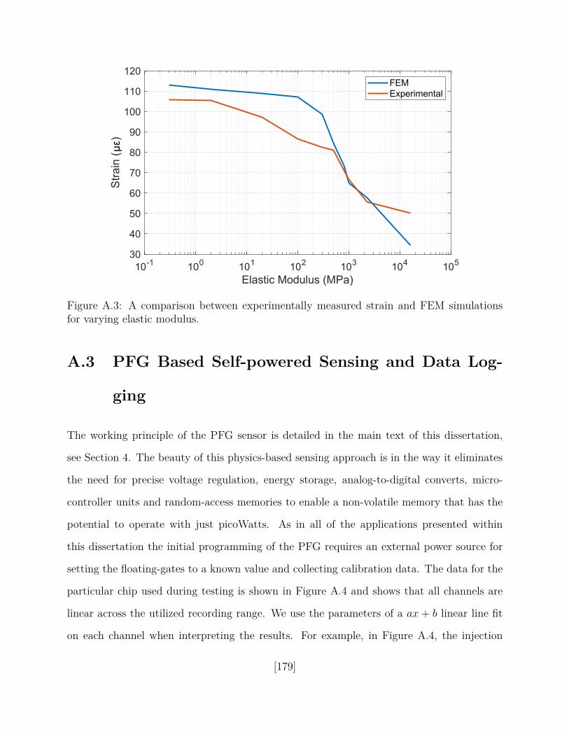
µε
Figure A.3: A comparison between experimentally measured strain and FEM simulationsfor varying elastic modulus.
A.3 PFG Based Self-powered Sensing and Data Log-
ging
The working principle of the PFG sensor is detailed in the main text of this dissertation,
see Section 4. The beauty of this physics-based sensing approach is in the way it eliminates
the need for precise voltage regulation, energy storage, analog-to-digital converts, micro-
controller units and random-access memories to enable a non-volatile memory that has the
potential to operate with just picoWatts. As in all of the applications presented within
this dissertation the initial programming of the PFG requires an external power source for
setting the floating-gates to a known value and collecting calibration data. The data for the
particular chip used during testing is shown in Figure A.4 and shows that all channels are
linear across the utilized recording range. We use the parameters of a ax + b linear line fit
on each channel when interpreting the results. For example, in Figure A.4, the injection
[179]
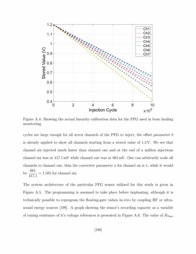
0 2 4 6 8 10
Injection Cycle x105
0.4
0.5
0.6
0.7
0.8
0.9
1
1.1
1.2
Sto
red
Va
lue
(V
)
Ch1
Ch2
Ch3
Ch4
Ch5
Ch6
Ch7
Figure A.4: Showing the actual linearity calibration data for the PFG used in bone healingmonitoring.
cycles are large enough for all seven channels of the PFG to inject, the offset parameter b
is already applied to show all channels starting from a stored value of 1.2 V. We see that
channel six injected much faster than channel one and at the end of a million injections
channel six was at 417.1 mV while channel one was at 661 mV. One can arbitrarily scale all
channels to channel one, thus the corrective parameter a for channel on is 1, while it would
be661
417.1= 1.585 for channel six.
The system architecture of the particular PFG sensor utilized for this study is given in
Figure A.5. The programming is assumed to take place before implanting, although it is
technically possible to reprogram the floating-gate values in-vivo by coupling RF or ultra-
sound energy sources [199]. A graph showing the sensor’s recording capacity as a variable
of tuning resistance of it’s voltage references is presented in Figure A.6. The value of RTune
[180]

N1
P1
−
+
VIn N3
N6 N7
N4
P6
P4
N5
P7
P5
Vb1
Vb2
N2
VNN
RTune
Programming Mode
Self-powering Mode
Piezo +
Piezo -
VOUT
Next
ResetInject
Tunnel
VInj
VTun
Vdda
Vddp
RTune
Protection
& Rectifier
Time
Dilation
Injection
Control
Voltage
Reference
Pulse
ADC
Injection
Charge Pump
Digital
Control
Ring
Oscillator
Tunneling
Charge Pump
P3
P2 VSelect
VTun
SInj
−
+VR ef
Vddp
MFG
I Ref
Vdda
......
...
Vdd
N1
x(t)
External Power
(Ultrasound, RF, etc.)
Figure A.5: A system architecture of the PFG sensor chipset with schematics for self-poweredblocks.
was selected to allow 200 000 cycles of injection, sourcing a readily-available resistor resulted
in the particular value of 3.2 MΩ. The applied force for each loading cycle was 600 N at
2 Hz, as this is the loading used for the longer-term testing (explained in the next subsec-
tion). Measured parameters of the PFG are given in Table A.1 and micrograph of the actual
variant of the PFG is presented as Figure A.7.
[181]
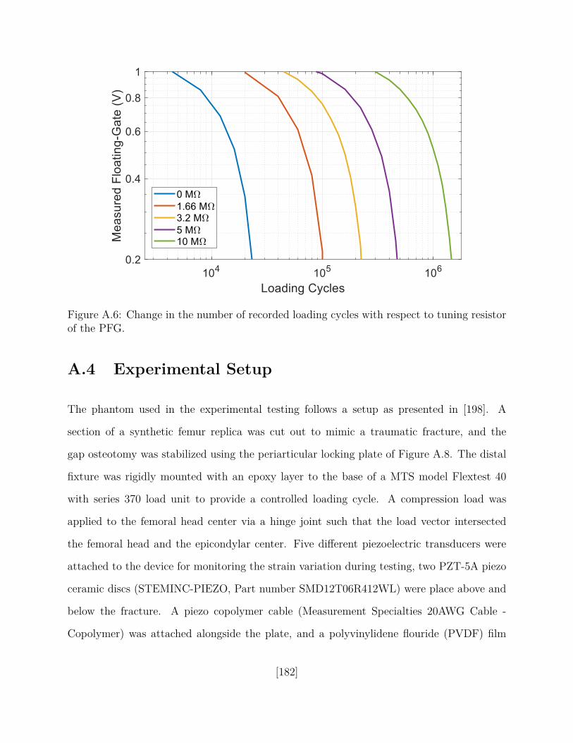
Figure A.6: Change in the number of recorded loading cycles with respect to tuning resistorof the PFG.
A.4 Experimental Setup
The phantom used in the experimental testing follows a setup as presented in [198]. A
section of a synthetic femur replica was cut out to mimic a traumatic fracture, and the
gap osteotomy was stabilized using the periarticular locking plate of Figure A.8. The distal
fixture was rigidly mounted with an epoxy layer to the base of a MTS model Flextest 40
with series 370 load unit to provide a controlled loading cycle. A compression load was
applied to the femoral head center via a hinge joint such that the load vector intersected
the femoral head and the epicondylar center. Five different piezoelectric transducers were
attached to the device for monitoring the strain variation during testing, two PZT-5A piezo
ceramic discs (STEMINC-PIEZO, Part number SMD12T06R412WL) were place above and
below the fracture. A piezo copolymer cable (Measurement Specialties 20AWG Cable -
Copolymer) was attached alongside the plate, and a polyvinylidene flouride (PVDF) film
[182]

Figure A.7: The micrograph of the actual, fabricated chip used for testing. A 10 nF tuningcapacitor and 3.2 MΩ resistor are located off-chip.
(model number DT2-052K/L with rivets) was attached on the inside of the implant. The
properties of these piezoelectrics are detailed in Table A.2. Finally, a commercial strain
gauge was placed at the fracture centerline. A Crack Opening Displacement (COD) gauge
was used to verify the resulting compression of the osteotomy gap at the far cortex. Each
piezoelectric was connected to the PFG sensor board (bottom left of Figure A.8 to record
the cumulative history of voltage variation.
[183]
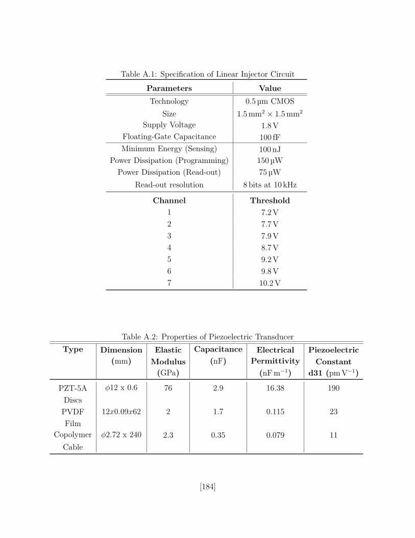
Table A.1: Specification of Linear Injector Circuit
Parameters Value
Technology 0.5 µm CMOS
Size 1.5 mm2 × 1.5 mm2
Supply Voltage 1.8 V
Floating-Gate Capacitance 100 fF
Minimum Energy (Sensing) 100 nJ
Power Dissipation (Programming) 150 µW
Power Dissipation (Read-out) 75 µW
Read-out resolution 8 bits at 10 kHz
Channel Threshold
1 7.2 V
2 7.7 V
3 7.9 V
4 8.7 V
5 9.2 V
6 9.8 V
7 10.2 V
Table A.2: Properties of Piezoelectric Transducer
Type Dimension Elastic Capacitance Electrical Piezoelectric
(mm) Modulus (nF) Permittivity Constant
(GPa) (nF m−1) d31 (pm V−1)
PZT-5A φ12 x 0.6 76 2.9 16.38 190
Discs
PVDF 12x0.09x62 2 1.7 0.115 23
Film
Copolymer φ2.72 x 240 2.3 0.35 0.079 11
Cable
[184]
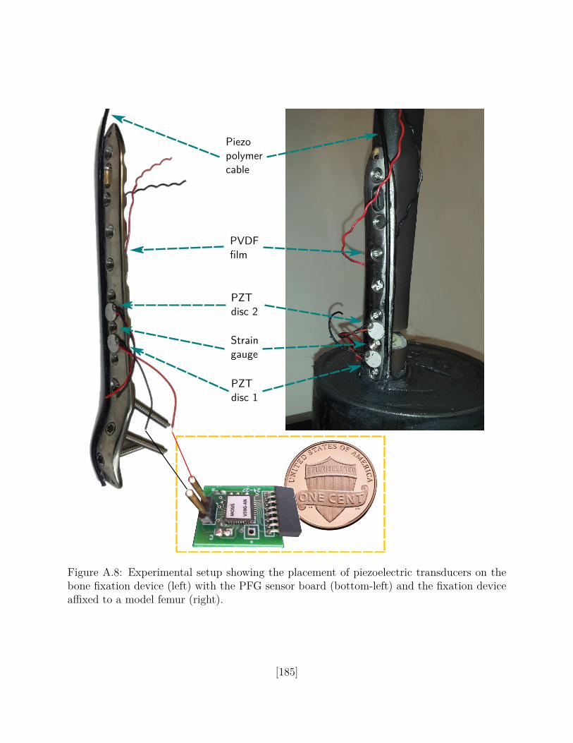
PVDF
film
Piezo
polymer
cable
Strain
gauge
PZT
disc 1
PZT
disc 2
Figure A.8: Experimental setup showing the placement of piezoelectric transducers on thebone fixation device (left) with the PFG sensor board (bottom-left) and the fixation deviceaffixed to a model femur (right).
[185]

In the first set of experiments, the healing period was simulated with 2000 cycles of loading
of a 420 N cyclic axial load at 2 Hz frequency to the femoral head center. This loading force
was selected to be lower than the expected 1870 N levels from walking [200]. Before any
simulated healing, these loads were sufficient for causing injection across all seven channels
of the PFG. Data were collected for 2000 cycles with the osteotomy left flexible to simulate
a non-healing case. In the second test, a quickly-healing case is emulated by swapping
out different materials in the osteotomy with increasing elastic modulus every 200 cycles as
detailed in Figure A.9. For the composite materials, layers of hard silicone and thin aluminum
plates were stacked to achieve the desired elastic modulus (higher ratio of aluminum to
silicone results in higher elastic modulus). In a more realistic scenario, a complete fracture
might have a healing period of four months and can be simulated with 200 000 cycles of
loading [201]. In this testing, the applied force was increased to 600 N while maintaining the
2 Hz cycle rate. The progression of materials used to mimic a more slowly healing bone is
given in Figure A.10. In this case, a non-healing condition is modeled by applying the full
200 000 cycles without any materials inside the osteotomy, whereas a healing case swaps out
the material to fill the osteotomy every 20 000 cycles.
200
0.3
400
2
600
20
800
100
1000
300
1200
500
1400
800
1600
1000 2300
1800
16000
2000
flexi
ble
poly
mer fo
am
soft s
ilico
ne
hard
sili
cone
com
posi
te
wood
acr
ylic
bone
com
posi
te
com
posi
te
com
posi
te
Inserted
Material
E (MPa)
Cycles
Figure A.9: The materials and their elastic modulus along with when they were used withrespect to the number of cycles. This emulates a quickly-healing case.
[186]

20 40 60 10080 120 140 160 180 200
0.3 2 20 100 300 500 900 1000 2300 16000
220 240
600 700
flexi
ble
poly
mer fo
am
soft s
ilico
ne
hard
sili
cone
com
posi
tew
ood
acr
ylic
bone
com
posi
te
com
posi
te
com
posi
te
com
posi
te
com
posi
te
Inserted
Material
E (MPa)
Cycles (k)
Figure A.10: The materials and their elastic modulus along with when they were used withrespect to the number of cycles. This emulates a slowly-healing case.
A.5 Results
A.5.1 PFG Activation for Femur Loading
Due to the placement and low mechanical-to-electrical coupling coefficients, the PVDF film
and copolymer cable generated voltages below 1 V, which was insufficient for logging data on
this version of the PFG. The maximum observed voltages generated by the different types
of piezoelectrics is in Table A.3. PZT Disc 1 is the ceramic disc that was placed above
the fracture line. Femur loading caused compression and bending due to load eccentricity
that resulted in the ceramic disc placed below the fracture line, PZT Disc 2, being the best
option for recording all channels of the PFG. The results in this table were collected during
the non-healing test with loads of 420 N.
Table A.3: Maximum Generated Voltage by Piezoelectric
Piezo Transducer Generated (V)
PVDF Film 0.8 V
PZT Disc 1 2.4 V
PZT Disc 2 10.53 V
Copolymer 0.67 V
[187]

0 500 1000 1500 2000
Loading Cycles (n)
20
30
40
50
60
70
80
90
100
Inte
r-cycle
Varia
tion (
% initia
l) PZTStrain GaugeCOD Gauge
Figure A.11: Variability between the measurement devices of PZT Disc 2 (below fracture),strain gauge, and COD gauge. All three are in close agreement during the entire bone healingprocess.
Figure A.11 gives the different results observed across three types of piezoelectric transducers,
with respect to their initially observed values at the start of osteotomy compression. As the
fast bone healing process is simulated, all three modalities show similar rates of decreasing
voltage generated with increased gap stiffness (i.e. lower strain levels). These results verify
that PZT Disc 2 will enable the PFG to log statistics similar to the ground truth collected
using commercial, externally-powered strain sensors.
A.5.2 Logged Data for Healing Periods
As in Figure A.11, a comparison of the PZT Disc 2 against a standard strain gauge is
presented in Figure A.12. To reiterate, a measurement of 100 % would be the voltage
generated when the osteotomy is non-healed or filled with flexible material. As the material
in the gap increases in stiffness, the share of the load on the bone fixation plate decreases,
[188]

consequently the generated voltage on the piezoelectric transducer will decrease. A complete
snapshot showing the relative variation of the memory with respect to non-healing and
healing bones is presented as Figure A.13. The number of channels recording is only for
the healing case, in the non-healing case all seven channels always inject and the red line
shows a completely linear trend as expected from the PFG with linear injection feedback.
Table A.4 gives the actual load cycles at which certain PFG channels stopped recording,
note that channel one is the most sensitive, and each subsequent channel has approximately
one diode drop of additional voltage required to log data as highlighted in Table A.1.
0 20 40 60 80 100 120 140 160 180 200 220 240
Loading Cycles (x 1000 n)
0
10
20
30
40
50
60
70
80
90
100
Measu
rem
en
t V
alu
e V
aria
tio
n (
%)
PZT Voltage
Strain Gauge
0 0.3
2 20
10 3
00
500
600
700
900
1,0
00
2,3
00
16,0
00Elastic Modulus (MPa)
Figure A.12: Variability between the measurement devices of PZT Disc 2 (below fracture)and strain gauge for the slower bone healing simulation.
[189]
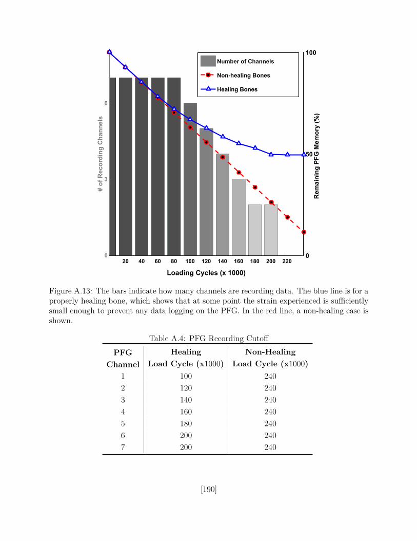
20 40 60 80 100 120 140 160 180 200 220
Loading Cycles (x 1000)
0
50
100
Number of Channels
Non-healing Bones
Healing Bones
Re
ma
inin
g P
FG
Me
mo
ry (
%)
0
3
6#
of
Re
co
rdin
g C
ha
nn
els
Figure A.13: The bars indicate how many channels are recording data. The blue line is for aproperly healing bone, which shows that at some point the strain experienced is sufficientlysmall enough to prevent any data logging on the PFG. In the red line, a non-healing case isshown.
Table A.4: PFG Recording Cutoff
PFG Healing Non-Healing
Channel Load Cycle (x1000) Load Cycle (x1000)
1 100 240
2 120 240
3 140 240
4 160 240
5 180 240
6 200 240
7 200 240
[190]

A.6 Discussion and Conclusion
This foray into a biomedical application shows the potential for using the PFG in energy-
constrained in-vivo measurement. In particular, bone healing of a femur was demonstrated.
Because the sensor is powered directly by the strain variations on the fixation device, it
achieves essentially continuous data logging that is not possible with conventional sensors on
the market. This experiment did not utilize wireless telemetry since it was to show feasibility,
but we have previously demonstrated the potential for RF and other wireless data retrieval
systems. The packaging and biocompatibility of the PZT transducers and PFG sensor was
not considered.
A major limitation in this approach is that the entire PFG sensor needs to be powered
using the piezoelectric transducer. In the presented form, such a sensor would require the
transducer to generate at least 7 V to have any meaningful data collection. Such large
voltages will require significant loading, thus precluding this method from being applied to
bones besides the femur, tibia, knee, or hip. The method also assumes that the sustained
injuries are not so significant as to prevent a patient from ambulating or walking about.
In the cases of bed-ridden or wheelchair-bound patients the PFG sensors would not record
any statistics as the bone fixation device would not be sufficiently loaded. To increase the
utility of a PFG-based monitoring of bone healing, the use of a more sensitive architecture,
as outlined in Section 5, is suggested. With data logging sensitivities potentially extending
down into the mV range, the modified PFG could record bone healing progress in many
more situations. With increased sensitivity, a similar method could even be applied for
monitoring of stents or sutures. This is a topic for future exploration and not detailed in
this dissertation.
[191]

Thanks to Dr. Aaron Purdue from University of Michigan and Dr. Hallie P. Brinkerhuff
from Zimmer-Biomet for their valuable comments and discussions regarding the progression
of bone-healing and the integration of the PFG sensors onto a fixation device. The material
in this appendix is based upon work supported in part by the National Science Founda-
tion STTR Phase I grant 1417044 (Sub-contract through Piezonix LLC.) and the Graduate
Research Fellowship Program under Grant Nos. DGE-0802267 and DGE-1143954. Any
opinions, findings, and conclusions or recommendations expressed in this material are those
of the author and do not necessarily reflect the views of the National Science Foundation.
[192]
Related Documents