Nanophotonics Prof. Albert Polman Center for Nanophotonics FOM-Institute AMOLF, Amsterdam Debye Institute, Utrecht University

Nanophotonics Prof. Albert Polman Center for Nanophotonics FOM-Institute AMOLF, Amsterdam Debye Institute, Utrecht University.
Dec 27, 2015
Welcome message from author
This document is posted to help you gain knowledge. Please leave a comment to let me know what you think about it! Share it to your friends and learn new things together.
Transcript

Nanophotonics
Prof. Albert Polman
Center for NanophotonicsFOM-Institute AMOLF, Amsterdam
Debye Institute, Utrecht University

Nanophotonics: defined by its applications • communications technology• lasers• solid-state lighting• data storage• lithography• (bio-)sensors• optical computers• solar cells• displays• medical imaging• light-activated medical therapies
Nanophotonics is a unique part of physics/chemistry/materials science because it combines
a wealth of scientific challenges with a large variety of near-term applications.
Large interest from industry infundamental research on nanophotonics

Optical fiber
core
cladding
shielding

Silica fiber transparent at 1.55 m
1012 Hz
1.3 m
1.55 m

Optical fiber: long distance communication

Length scales in photonics
km 1 mm
10 m 1 m = 5 m

Merging optics and electronicsrequires nanoscale optics
40 nm
Plasmonics Photonics
Electronicsfr
equ
ency
size1 m
10 GHz

Planar optical waveguide
Si
high indexlow index
1 mm

Photonic integrated circuits on silicon
1 mm
SiO2/Al2O3/SiO2/Si
Al2O3 technology by M.K. Smit et al., TUD

Optical clock distribution on a Si microprocessor
Intel Website
Photonicson silicon

http://www.ima.umn.edu/industrial/2002-2003/sigalas/sigalas.pdf
Computer interconnects hierarchy
Mihail M. Sigalas, Agilent Laboratories, Palo Alto, CA

Nanophotonics examples:Surface plasmons guide light to the
nanoscale
k
E
xz
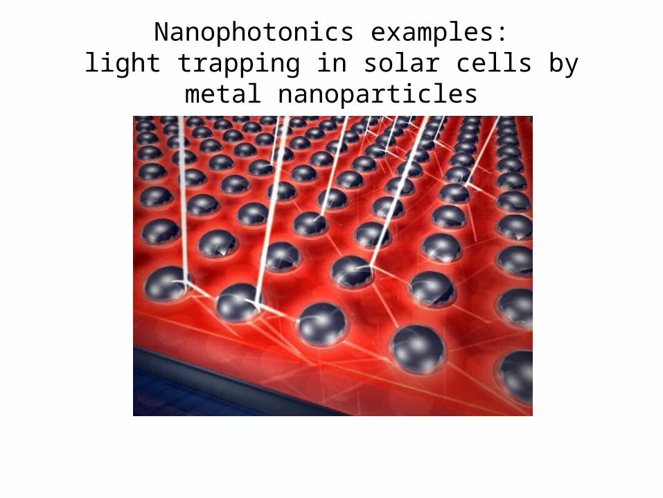
Nanophotonics examples:light trapping in solar cells by metal
nanoparticles

Nanophotonics examples:DNA assisted assembly of metal
nanoparticles
n=1.5
600nm

Nanophotonics examples:large-area fabrication of photonic
nanostructures
Marc Verschuuren, Philips Research

Nanophotonics examples:Exciting surface plasmons with an electron
beam

Nanophotonics examples:Light concentration in core-shell particles

Nanophotonics examples:Energy transfer in quantum dot / Er system

Nanophotonics examples:Anomalous transmission in metal hole arrays
Kobus Kuipers

Nanophotonics examples:Light emission from quantum dots

Nanophotonics examples:Multiple exciton generation in quantum dots
Mischa Bonn

Nanophotonics examples:Light emission from semiconductor
nanowires
4 m
Jaime Gomez Rivas

Nanophotonics examples:Controlled spontaneous emission in photonic
crystals
Willem Vos

What will you learn in this class?!
1) Theory of nanophotonics
2) Applications of nanophotonics
3) Nanophotonics fabrication techniques
4) New developments in science and technology
5) Presentation skills

Fabrication technology:• Thin film deposition• Clean room fabrication technology• Lithography• Focused ion beam milling• Colloidal self-assembly• Bio-templating
Characterization technology:• Photoluminescence spectroscopy• Optical absorption/extinction spectroscopy• Near-field microscopy• Cathodoluminescence imaging spectroscopy• Pump-probe spectroscopy
Practical training at FOM-Institute AMOLF

Weekly schedule
• Nanophotonics fundamentals• Fabrication technology• Characterization principles / techniques• Application examples• News of the week• Paper/homework presentations• Excursions/labtours
Albert PolmanE-mail: [email protected]: www.erbium.nl/nanophotonics

Class schedule
ALL DAY
ALL DAY
ALL MORNING

Course grading
No final examination
Grades are determined by:
Homework: 60 %Paper presentation 1: 10%Paper presentation 2: 15%Participation in class: 5%Nature Milestones 10 %
Homework must be handed next week Friday. No exceptions!Homework grade: average of (all homework – worst made)
Use help by teaching assistants!
Course time Friday, 11.00-13.00 hr.Absence: must be notified by e-mail
Related Documents