1 Nanometer-Scale InGaAs Field-Effect Transistors for THz and CMOS Technologies J. A. del Alamo Microsystems Technology Laboratories, MIT Acknowledgements: • D. Antoniadis, A. Guo, D.-H. Kim, T.-W. Kim, D. Jin, J. Lin, N. Waldron, L. Xia • Sponsors: Intel, FCRP-MSD, ARL, SRC • Labs at MIT: MTL, NSL, SEBL ESSDERC-ESSCIRC 2013 Bucharest, Romania, September 16-20, 2013

Welcome message from author
This document is posted to help you gain knowledge. Please leave a comment to let me know what you think about it! Share it to your friends and learn new things together.
Transcript
1
Nanometer-Scale InGaAs Field-Effect Transistors for THz and CMOS Technologies
J. A. del Alamo
Microsystems Technology Laboratories, MIT
Acknowledgements:• D. Antoniadis, A. Guo, D.-H. Kim, T.-W. Kim, D. Jin, J. Lin, N. Waldron, L. Xia• Sponsors: Intel, FCRP-MSD, ARL, SRC• Labs at MIT: MTL, NSL, SEBL
ESSDERC-ESSCIRC 2013Bucharest, Romania, September 16-20, 2013
1. InGaAs HEMT today
2. InGaAs HEMTs towards THz operation
3. InGaAs MOSFETs: towards sub-10 nm
CMOS
2
Outline
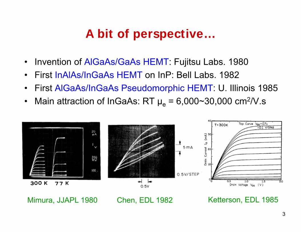
• Invention of AlGaAs/GaAs HEMT: Fujitsu Labs. 1980 • First InAlAs/InGaAs HEMT on InP: Bell Labs. 1982• First AlGaAs/InGaAs Pseudomorphic HEMT: U. Illinois 1985• Main attraction of InGaAs: RT μe = 6,000~30,000 cm2/V.s
A bit of perspective…
3
Mimura, JJAPL 1980 Ketterson, EDL 1985Chen, EDL 1982
4
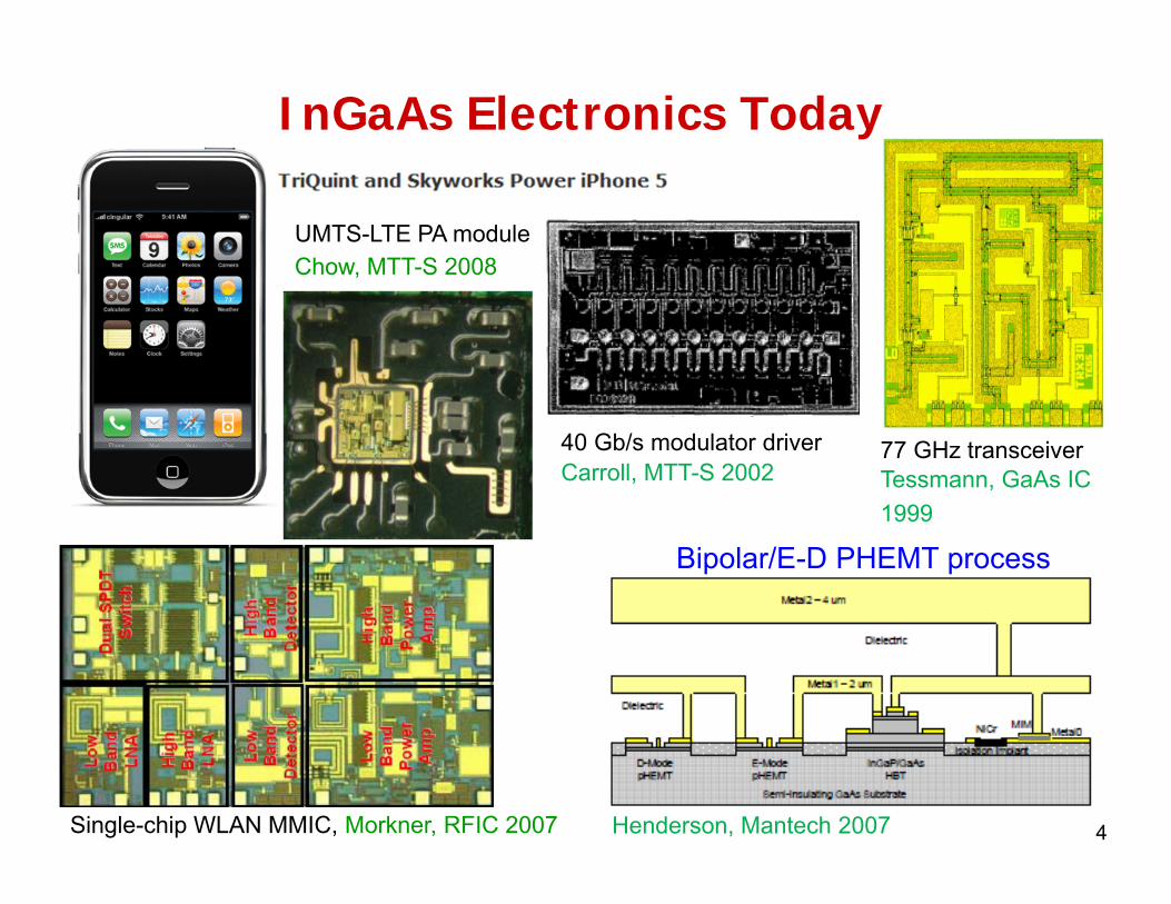
Bipolar/E-D PHEMT process
Henderson, Mantech 2007
40 Gb/s modulator driverTessmann, GaAs IC 1999
77 GHz transceiverCarroll, MTT-S 2002
UMTS-LTE PA moduleChow, MTT-S 2008
Single-chip WLAN MMIC, Morkner, RFIC 2007
InGaAs Electronics Today
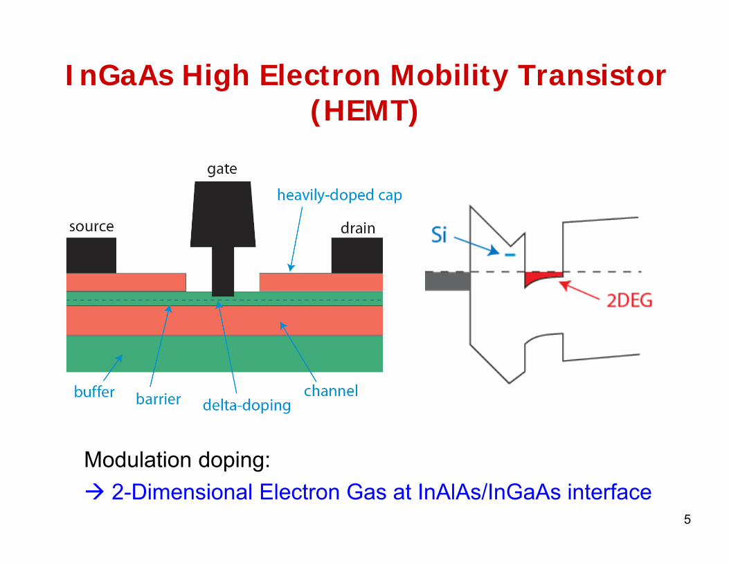
InGaAs High Electron Mobility Transistor (HEMT)
5
Modulation doping: 2-Dimensional Electron Gas at InAlAs/InGaAs interface
0
100
200
300
400
500
600
700
800
1980 1990 2000 2010
f T(GHz)
Year
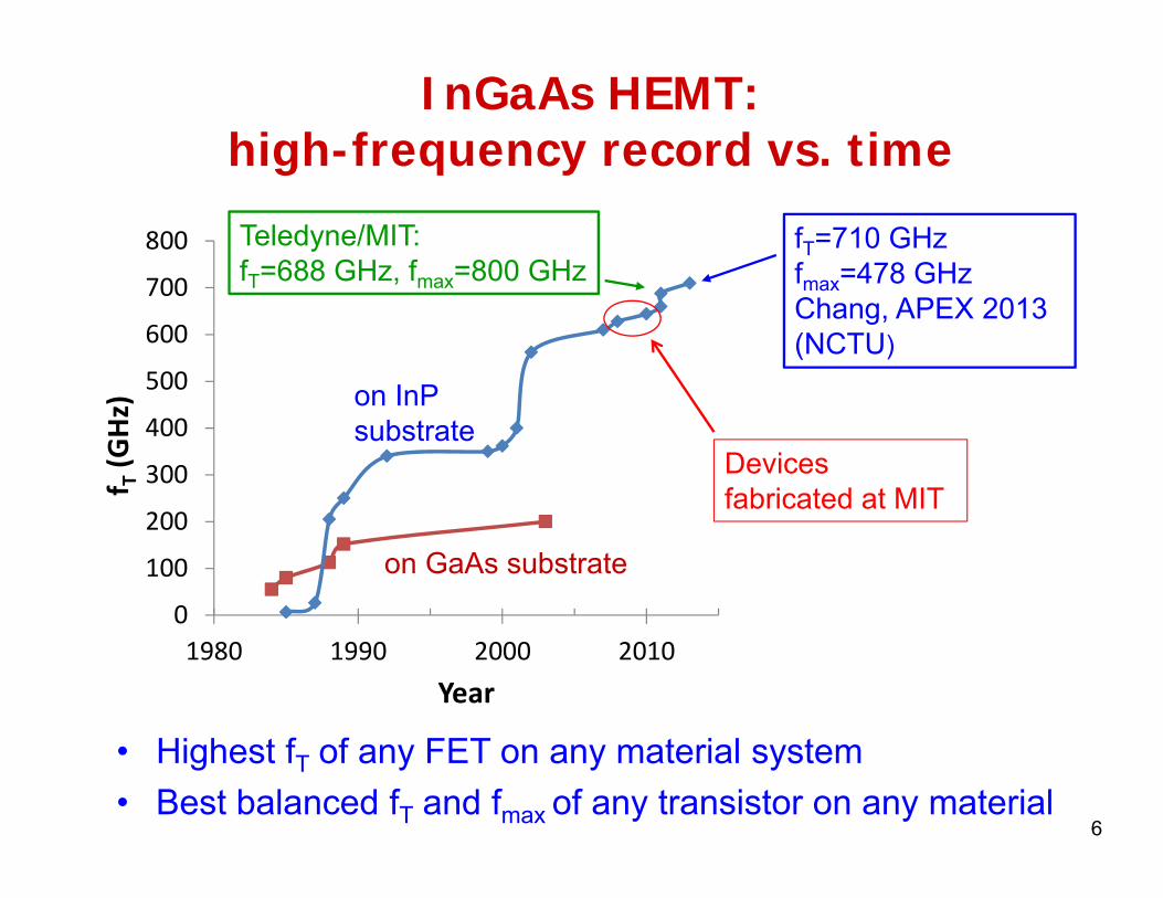
InGaAs HEMT: high-frequency record vs. time
6
• Highest fT of any FET on any material system• Best balanced fT and fmax of any transistor on any material
Teledyne/MIT: fT=688 GHz, fmax=800 GHz
Devices fabricated at MIT
on GaAs substrate
on InP substrate
fT=710 GHzfmax=478 GHzChang, APEX 2013 (NCTU)
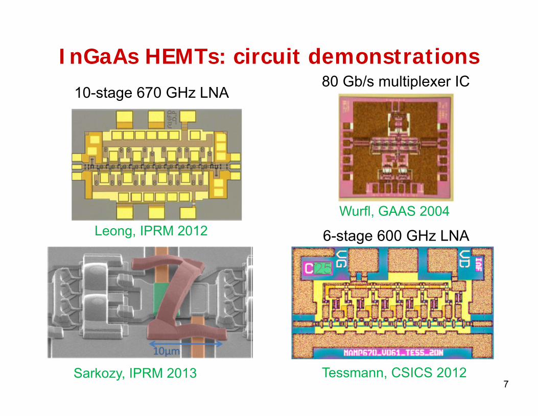
InGaAs HEMTs: circuit demonstrations
7
10-stage 670 GHz LNA80 Gb/s multiplexer IC
Wurfl, GAAS 2004
6-stage 600 GHz LNA
Tessmann, CSICS 2012
Leong, IPRM 2012
Sarkozy, IPRM 2013
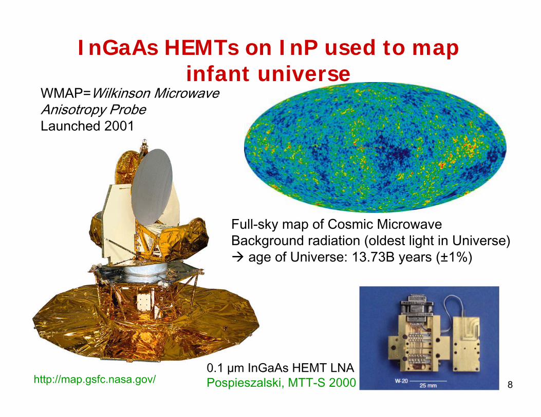
InGaAs HEMTs on InP used to map infant universe
8
Full-sky map of Cosmic MicrowaveBackground radiation (oldest light in Universe) age of Universe: 13.73B years (±1%)
WMAP=Wilkinson Microwave Anisotropy ProbeLaunched 2001
0.1 µm InGaAs HEMT LNA Pospieszalski, MTT-S 2000http://map.gsfc.nasa.gov/
99
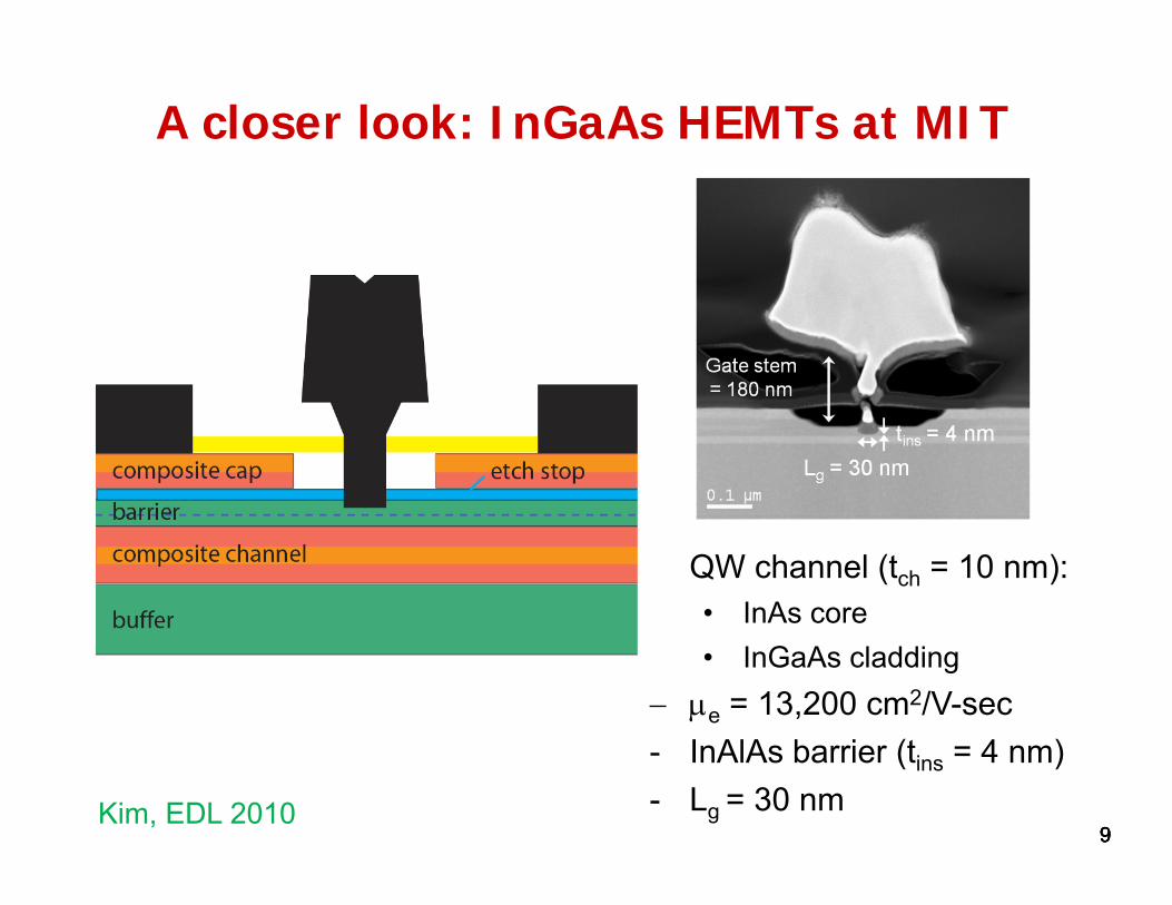
A closer look: InGaAs HEMTs at MIT
99
- QW channel (tch = 10 nm):• InAs core • InGaAs cladding
e = 13,200 cm2/V-sec- InAlAs barrier (tins = 4 nm)- Lg = 30 nmKim, EDL 2010
109 1010 1011 10120
10
20
30
40
Frequency [Hz]
Gai
ns [d
B]
-1
0
1
2
3
K
H21
K
MSG/MAG
Ug
1010
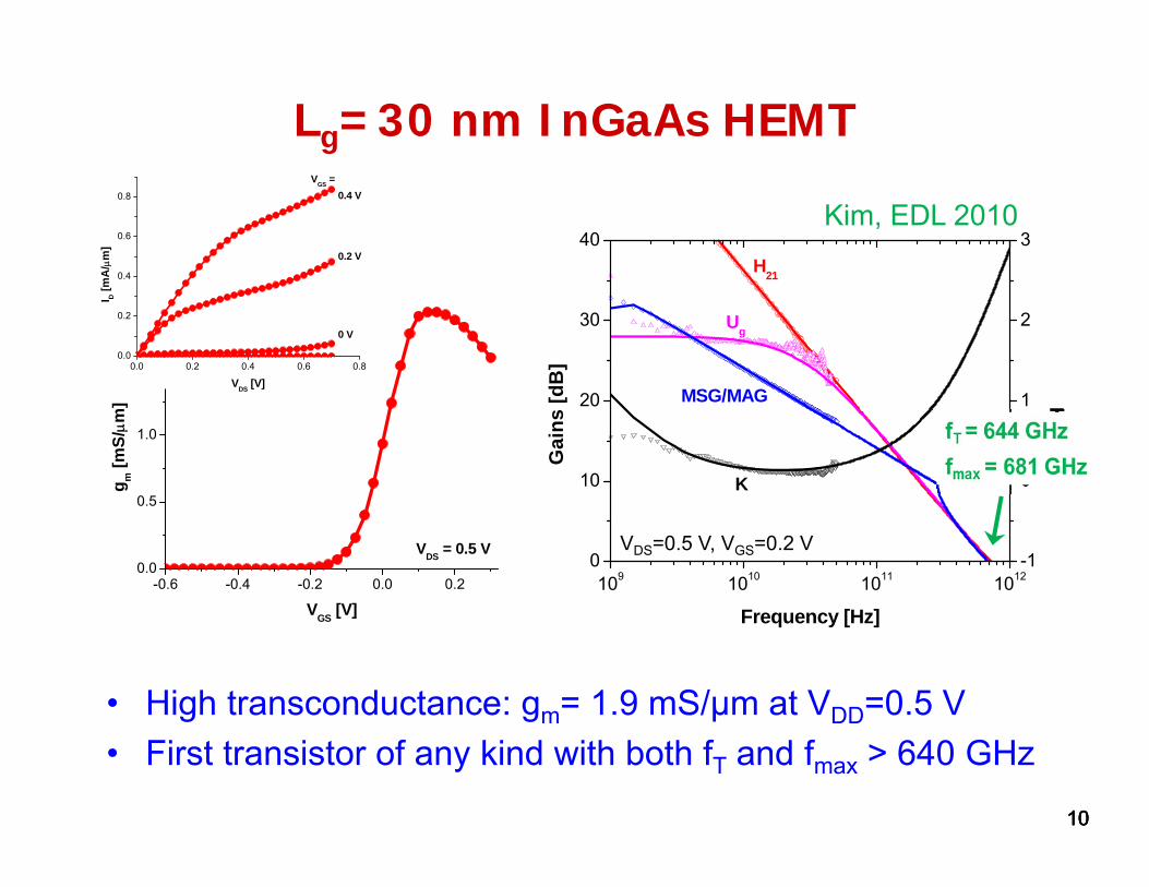
Lg=30 nm InGaAs HEMT
10
• High transconductance: gm= 1.9 mS/μm at VDD=0.5 V • First transistor of any kind with both fT and fmax > 640 GHz
10
Kim, EDL 2010
-0.6 -0.4 -0.2 0.0 0.20.0
0.5
1.0
1.5
2.0
g m [m
S/m
]
VGS [V]
VDS = 0.5 V
0.0 0.2 0.4 0.6 0.80.0
0.2
0.4
0.6
0.8
0.2 V
0.4 V
0 V
I D [m
A/
m]
VDS [V]
VGS =
VDS=0.5 V, VGS=0.2 V
11
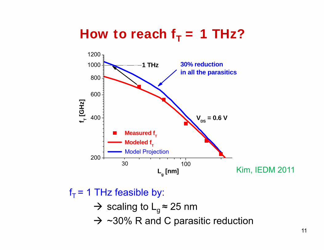
How to reach fT = 1 THz?
fT = 1 THz feasible by: scaling to Lg ≈ 25 nm ~30% R and C parasitic reduction
100200
400
600
800
1000
1200
VDS = 0.6 V
30% reductionin all the parasitics
Measured fT
Modeled fT
Model Projection
f T [GH
z]
Lg [nm]
1 THz
30Kim, IEDM 2011
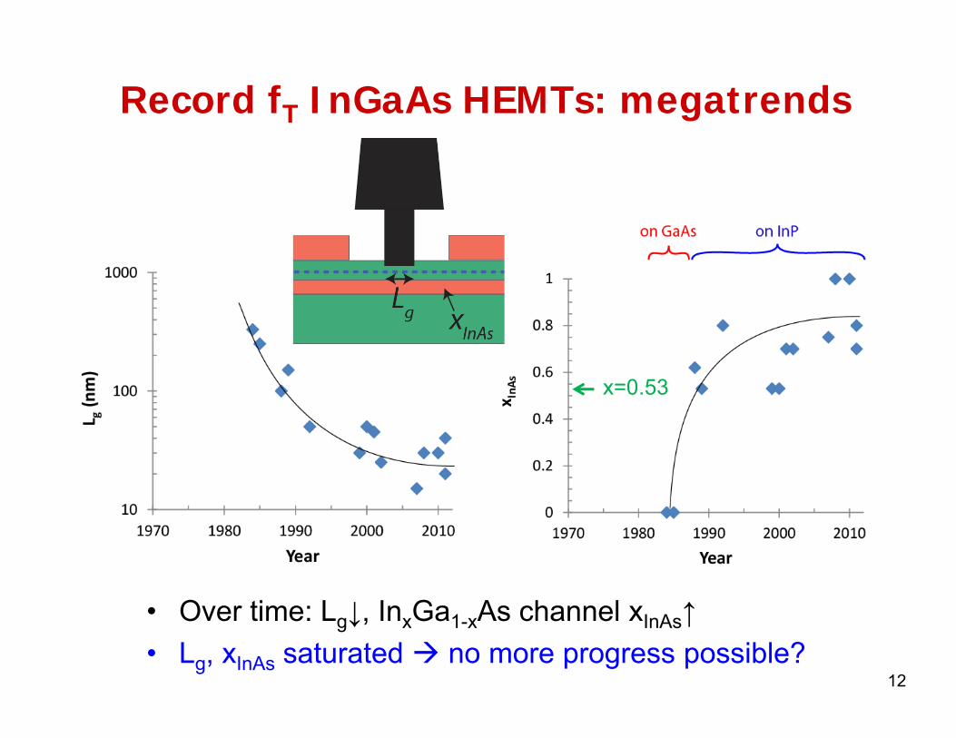
Record fT InGaAs HEMTs: megatrends
12
• Over time: Lg↓, InxGa1-xAs channel xInAs↑• Lg, xInAs saturated no more progress possible?
x=0.53
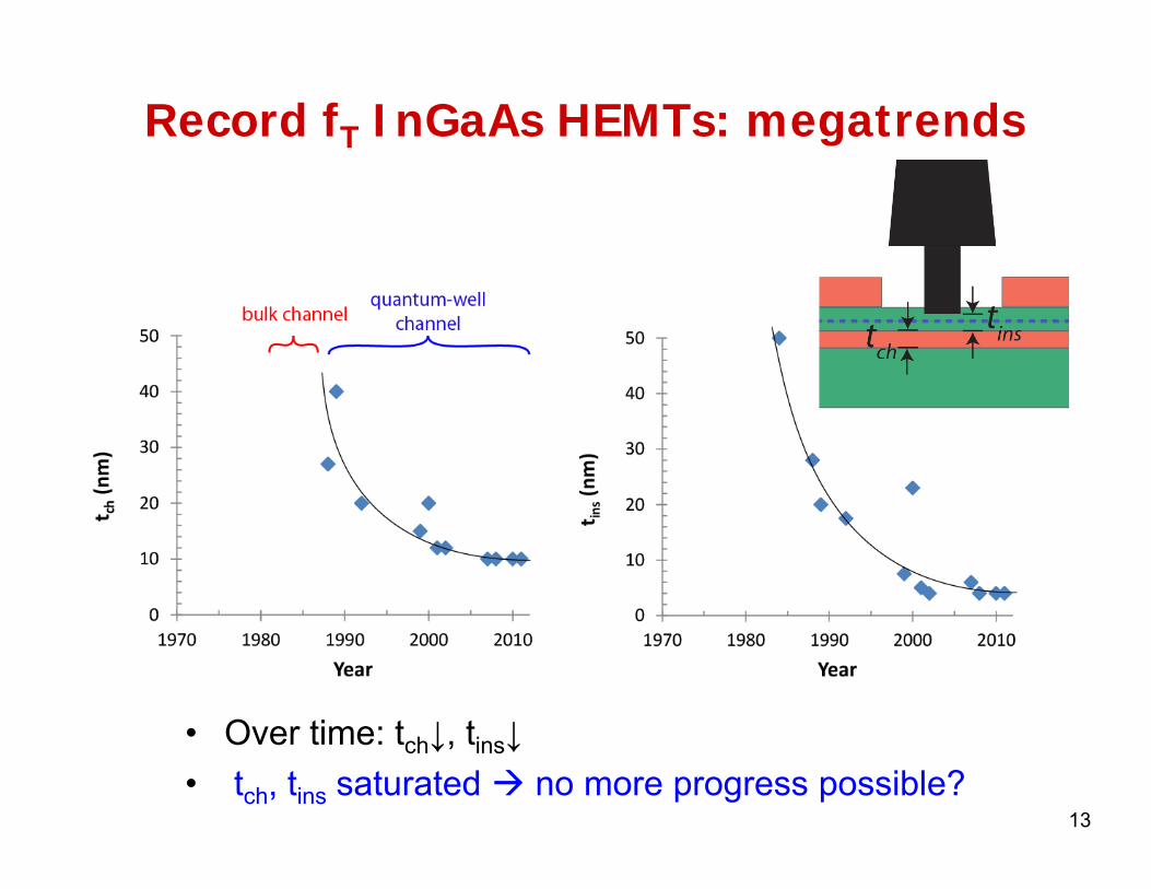
Record fT InGaAs HEMTs: megatrends
13
• Over time: tch↓, tins↓• tch, tins saturated no more progress possible?
14
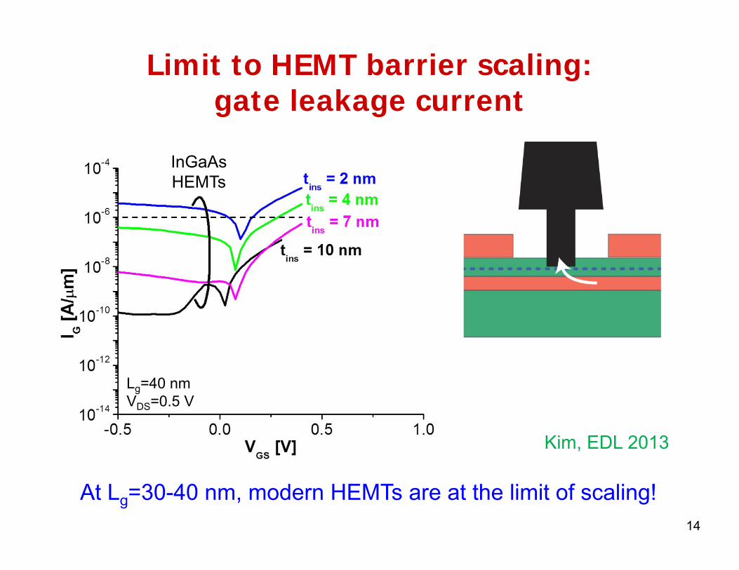
Limit to HEMT barrier scaling: gate leakage current
InGaAsHEMTs
At Lg=30-40 nm, modern HEMTs are at the limit of scaling!
Lg=40 nmVDS=0.5 V
Kim, EDL 2013
15
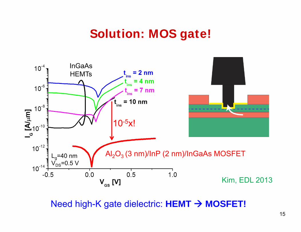
Solution: MOS gate!
Need high-K gate dielectric: HEMT MOSFET!
InGaAsHEMTs
10-5x!
Lg=40 nmVDS=0.5 V
Kim, EDL 2013
Al2O3 (3 nm)/InP (2 nm)/InGaAs MOSFET
16
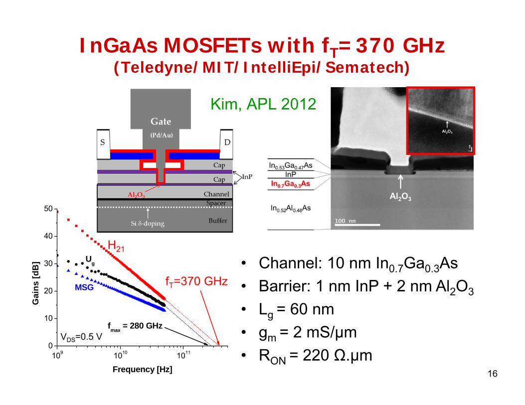
InGaAs MOSFETs with fT=370 GHz(Teledyne/MIT/IntelliEpi/Sematech)
• Channel: 10 nm In0.7Ga0.3As• Barrier: 1 nm InP + 2 nm Al2O3
• Lg = 60 nm• gm = 2 mS/μm• RON = 220 Ω.μm109 1010 1011
0
10
20
30
40
50
fmax = 280 GHz
MSG
Ug
Gai
ns [d
B]
Frequency [Hz]
H21
fT = 370 GHz
VDS=0.5 V
H21
Kim, APL 2012
fT=370 GHz
17
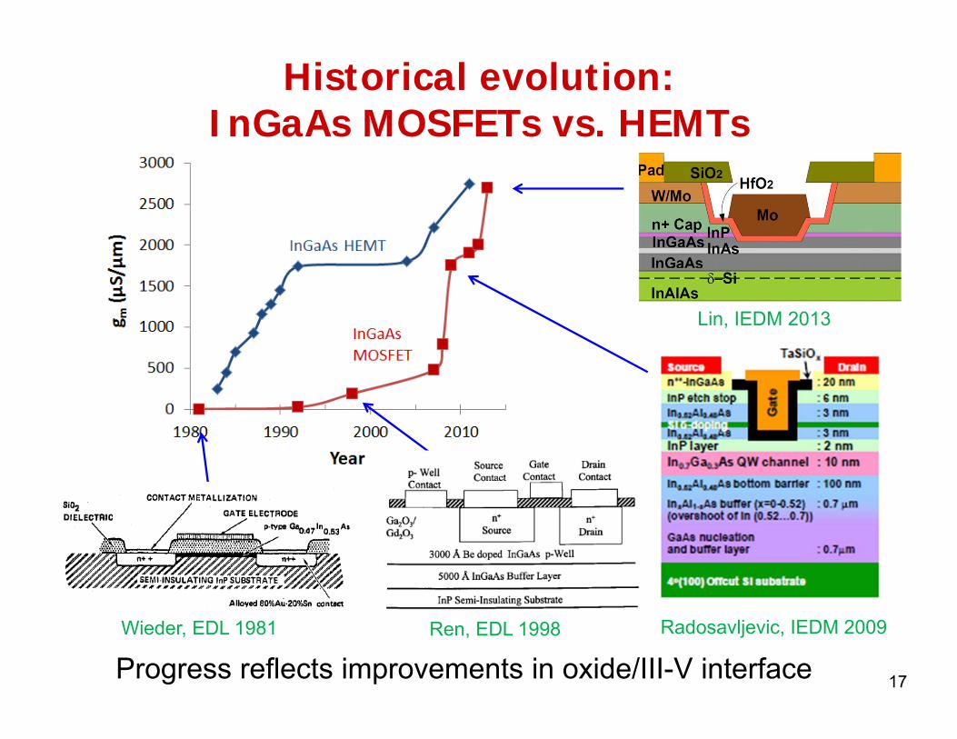
Historical evolution: InGaAs MOSFETs vs. HEMTs
Ren, EDL 1998 Radosavljevic, IEDM 2009Wieder, EDL 1981
Lin, IEDM 2013
Progress reflects improvements in oxide/III-V interface
18
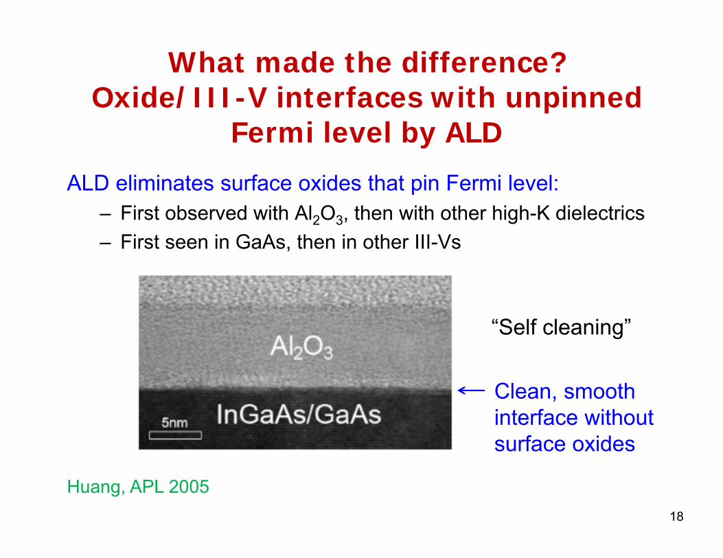
Huang, APL 2005
ALD eliminates surface oxides that pin Fermi level: – First observed with Al2O3, then with other high-K dielectrics– First seen in GaAs, then in other III-Vs
Clean, smooth interface without surface oxides
What made the difference?Oxide/III-V interfaces with unpinned
Fermi level by ALD
“Self cleaning”
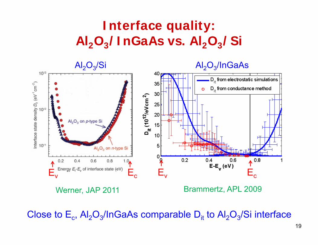
Interface quality: Al2O3/InGaAs vs. Al2O3/Si
19
Close to Ec, Al2O3/InGaAs comparable Dit to Al2O3/Si interface
Werner, JAP 2011
Al2O3/Si Al2O3/InGaAs
Brammertz, APL 2009
EcEvEv Ec
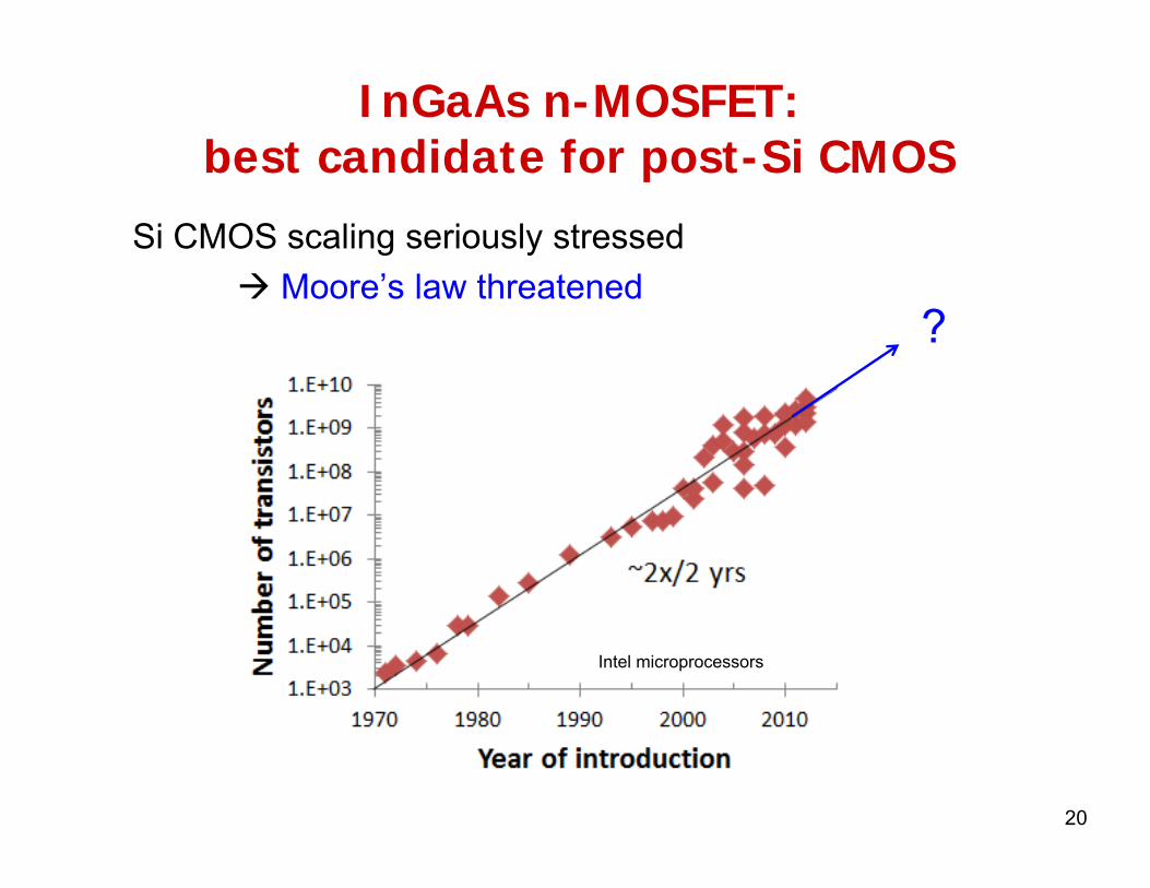
InGaAs n-MOSFET:best candidate for post-Si CMOS
Si CMOS scaling seriously stressed Moore’s law threatened
20
?
Intel microprocessors

21
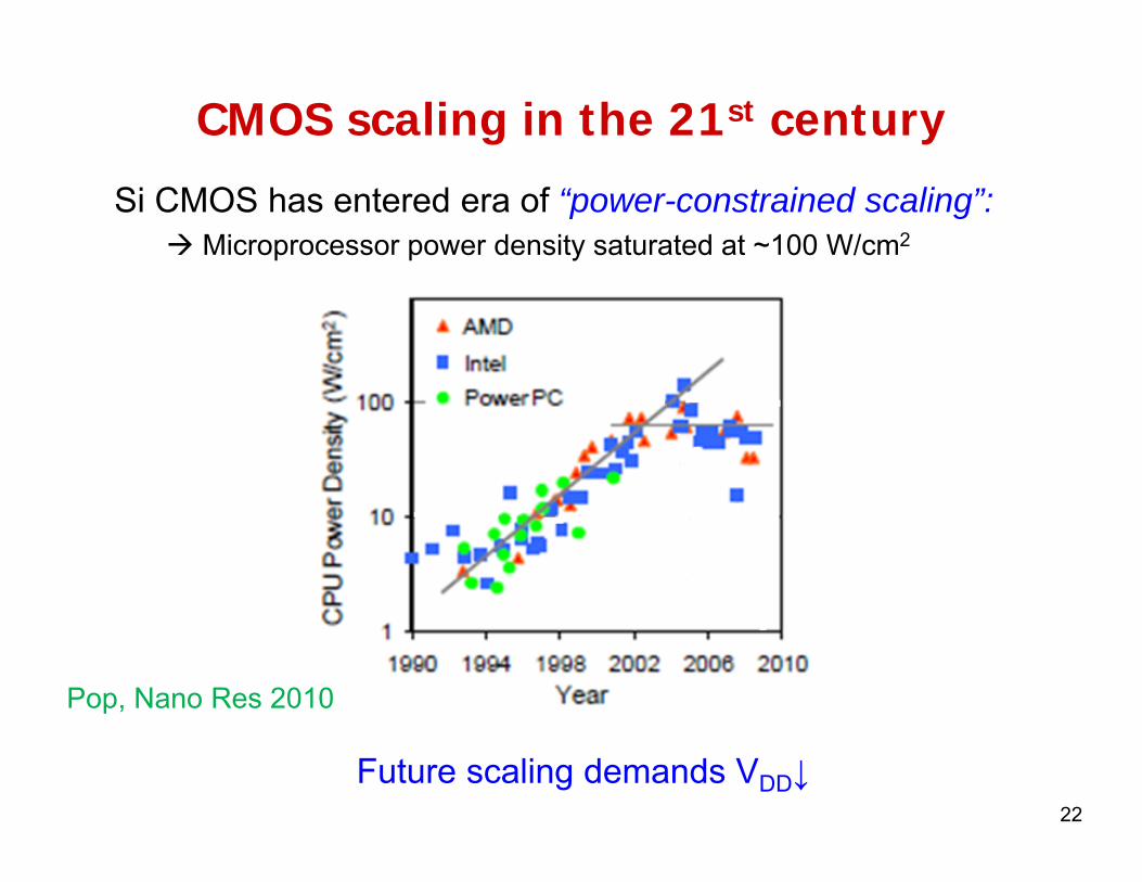
CMOS scaling in the 21st century
Si CMOS has entered era of “power-constrained scaling”: Microprocessor power density saturated at ~100 W/cm2
22
Pop, Nano Res 2010
Future scaling demands VDD↓
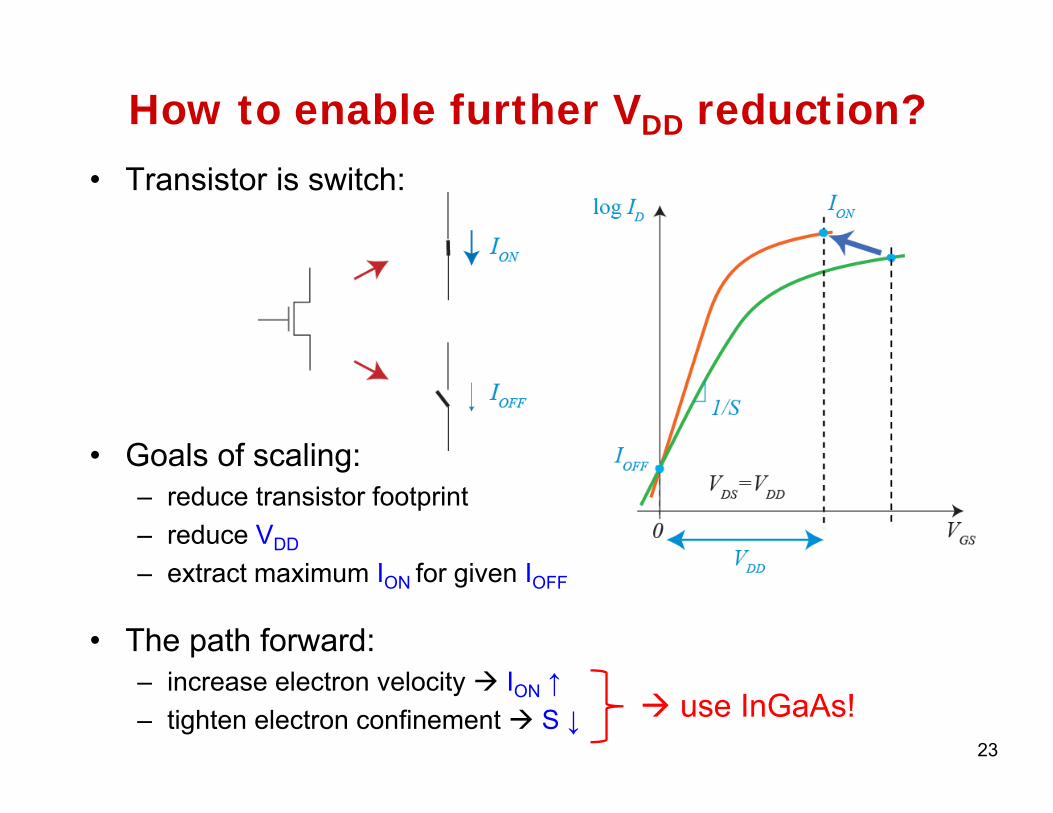
• Transistor is switch:
• Goals of scaling: – reduce transistor footprint– reduce VDD
– extract maximum ION for given IOFF
• The path forward:– increase electron velocity ION ↑ – tighten electron confinement S ↓
23
use InGaAs!
How to enable further VDD reduction?
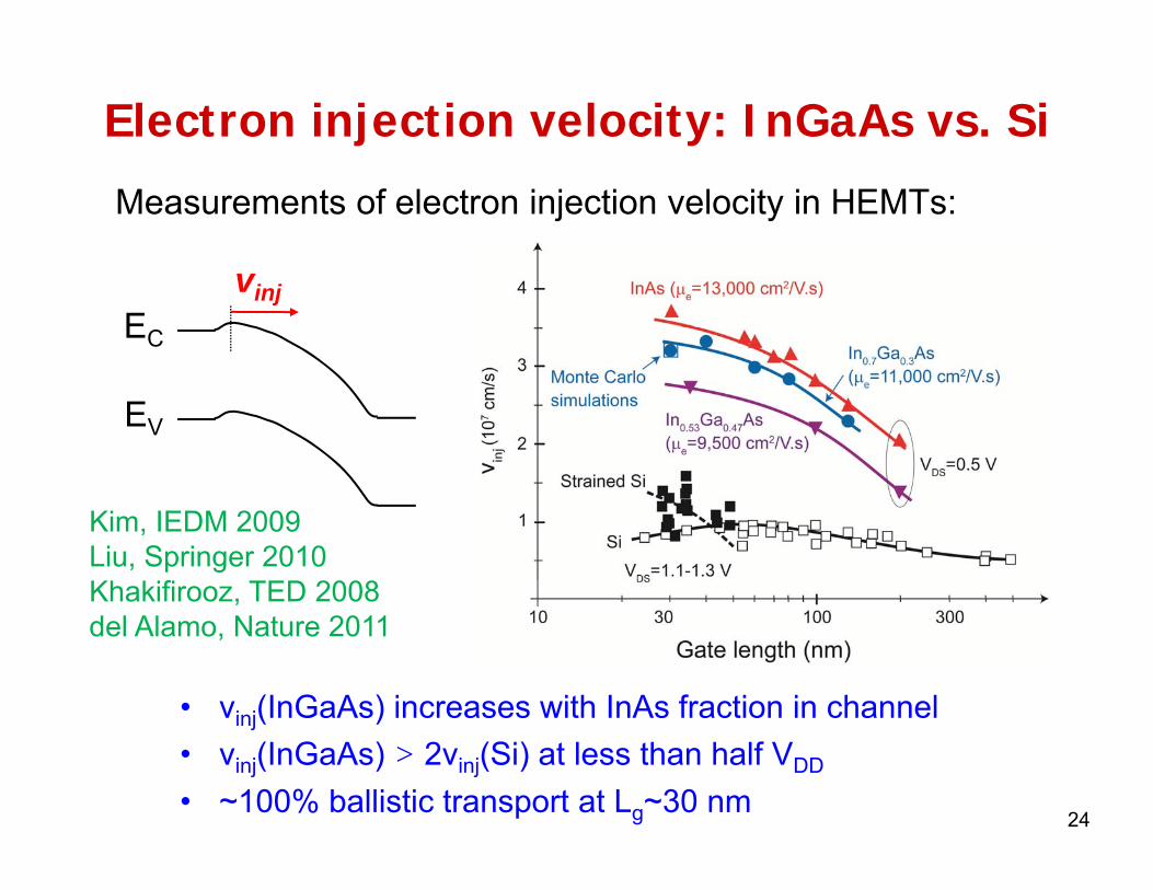
Measurements of electron injection velocity in HEMTs:
EC
vinj
• vinj(InGaAs) increases with InAs fraction in channel• vinj(InGaAs) > 2vinj(Si) at less than half VDD
• ~100% ballistic transport at Lg~30 nm
Electron injection velocity: InGaAs vs. Si
Kim, IEDM 2009Liu, Springer 2010Khakifirooz, TED 2008del Alamo, Nature 2011
24
EV
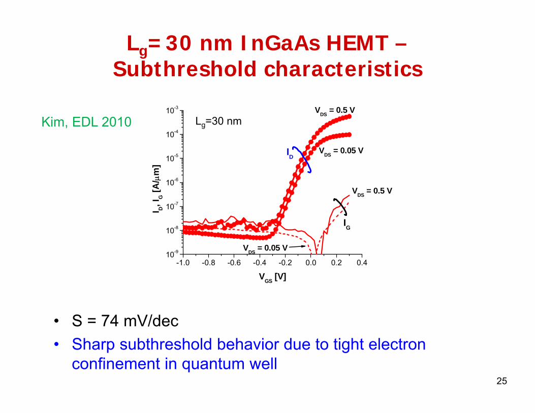
Lg=30 nm InGaAs HEMT –Subthreshold characteristics
25
• S = 74 mV/dec• Sharp subthreshold behavior due to tight electron
confinement in quantum well
Kim, EDL 2010
-1.0 -0.8 -0.6 -0.4 -0.2 0.0 0.2 0.410-9
10-8
10-7
10-6
10-5
10-4
10-3
VDS = 0.05 V
VDS = 0.5 V
IG
ID
VDS = 0.5 V
I D, I
G [A
/m
]
VGS [V]
VDS = 0.05 V
Lg=30 nm
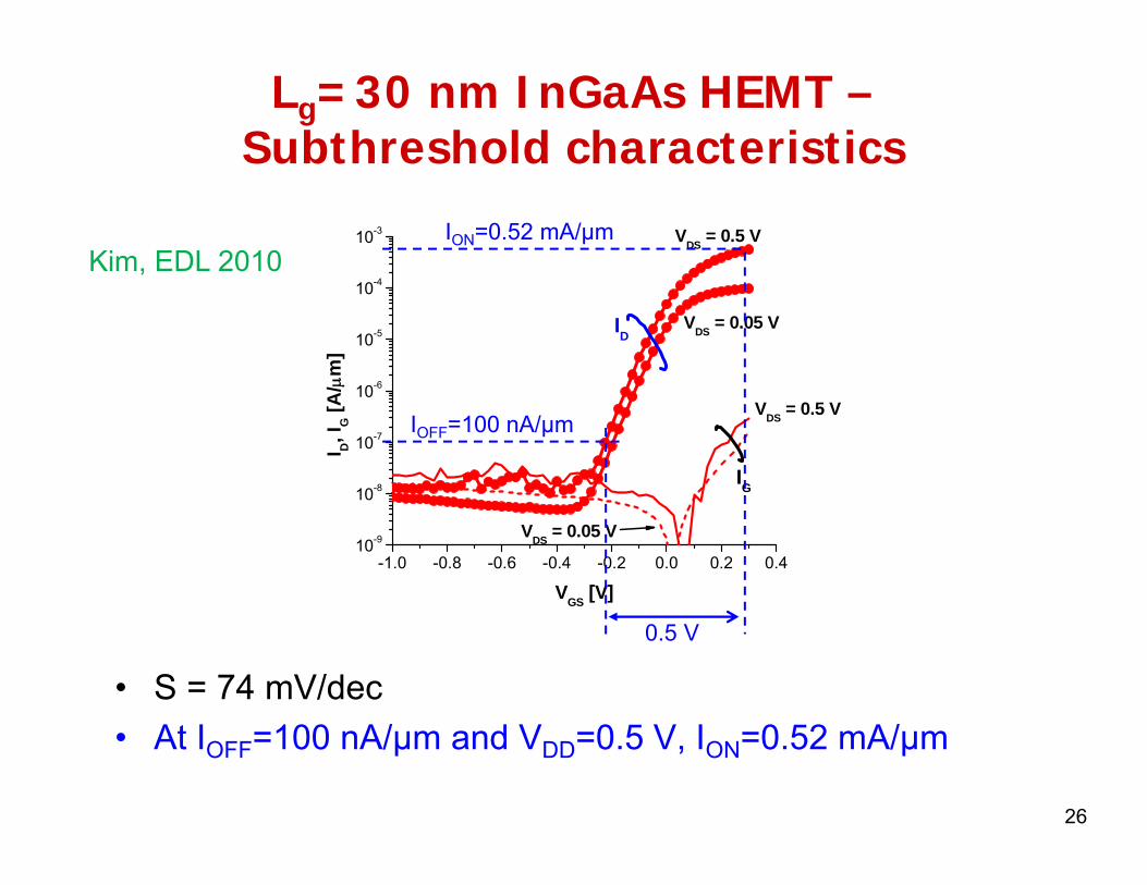
Lg=30 nm InGaAs HEMT –Subthreshold characteristics
26
• S = 74 mV/dec• At IOFF=100 nA/μm and VDD=0.5 V, ION=0.52 mA/μm
Kim, EDL 2010
-1.0 -0.8 -0.6 -0.4 -0.2 0.0 0.2 0.410-9
10-8
10-7
10-6
10-5
10-4
10-3
VDS = 0.05 V
VDS = 0.5 V
IG
ID
VDS = 0.5 V
I D, I
G [A
/m
]
VGS [V]
VDS = 0.05 V
ION=0.52 mA/μm
IOFF=100 nA/μm
0.5 V
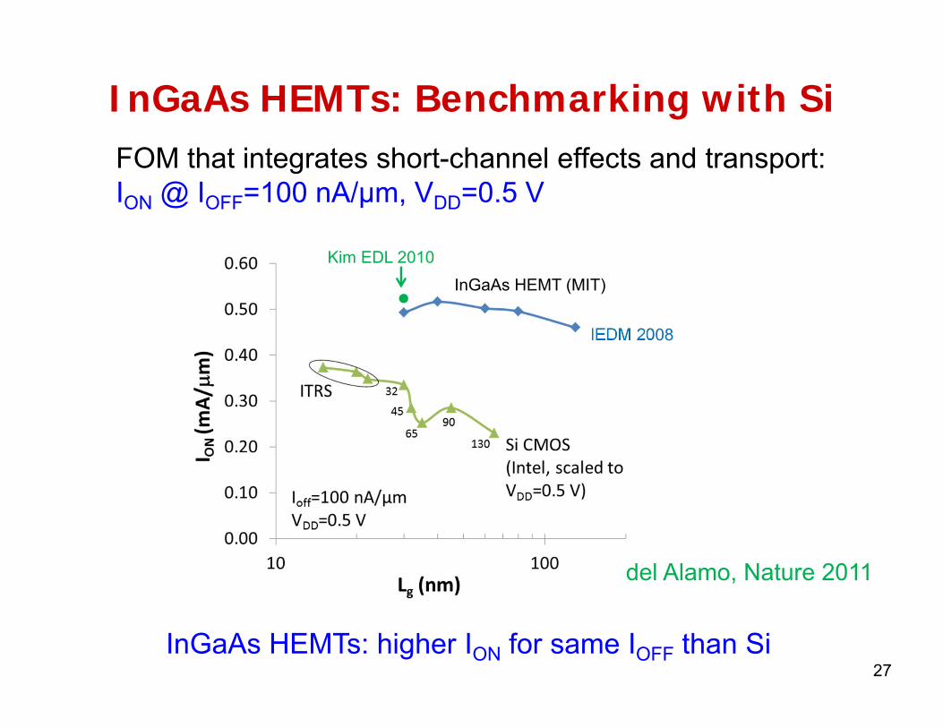
FOM that integrates short-channel effects and transport: ION @ IOFF=100 nA/µm, VDD=0.5 V
InGaAs HEMTs: higher ION for same IOFF than Si
InGaAs HEMTs: Benchmarking with Si
27
IEDM 2008
Kim EDL 2010InGaAs HEMT (MIT)
del Alamo, Nature 2011
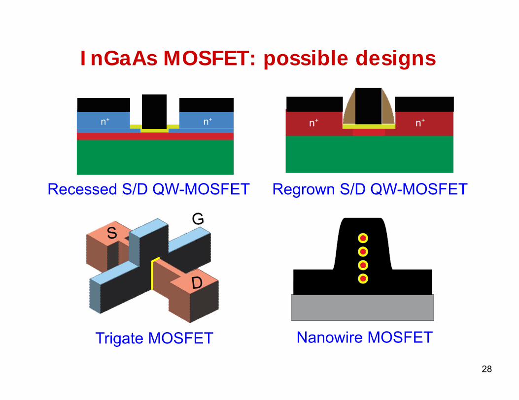
n+n+
InGaAs MOSFET: possible designs
Regrown S/D QW-MOSFET
Trigate MOSFET Nanowire MOSFET
Recessed S/D QW-MOSFET
28
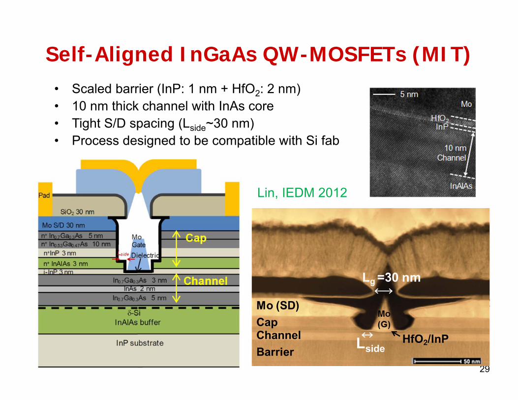
Self-Aligned InGaAs QW-MOSFETs (MIT)• Scaled barrier (InP: 1 nm + HfO2: 2 nm)• 10 nm thick channel with InAs core• Tight S/D spacing (Lside~30 nm)• Process designed to be compatible with Si fab
Lin, IEDM 2012
29
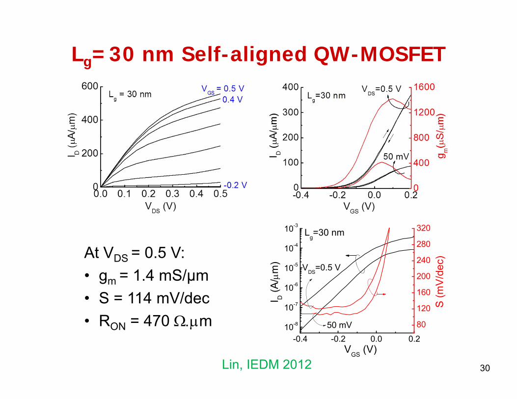
30
Lg=30 nm Self-aligned QW-MOSFET
At VDS = 0.5 V:• gm = 1.4 mS/µm• S = 114 mV/dec• RON = 470 m
Lin, IEDM 2012
-0.4 -0.2 0.0 0.210-8
10-7
10-6
10-5
10-4
10-3
S (m
V/d
ec)
50 mV
I D (A
/m
)
VGS (V)
VDS=0.5 V
Lg=30 nm
80
120
160
200
240
280
320
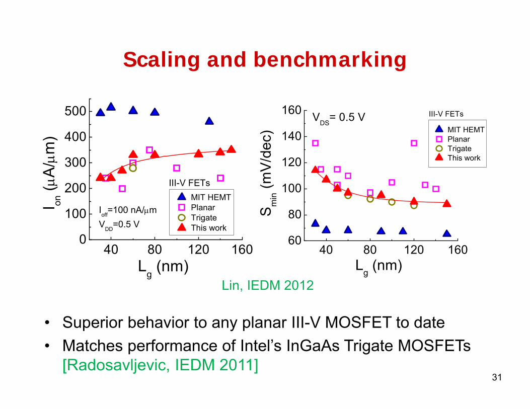
Scaling and benchmarking
• Superior behavior to any planar III-V MOSFET to date• Matches performance of Intel’s InGaAs Trigate MOSFETs
[Radosavljevic, IEDM 2011]31
Lin, IEDM 2012
40 80 120 1600
100
200
300
400
500
III-V FETs
I on (
A/
m)
Lg (nm)
Ioff=100 nA/mVDD=0.5 V
MIT HEMTPlanarTrigateThis work
40 80 120 16060
80
100
120
140
160 III-V FETsVDS= 0.5 VMIT HEMTPlanarTrigateThis work
Sm
in (m
V/d
ec)
Lg (nm)
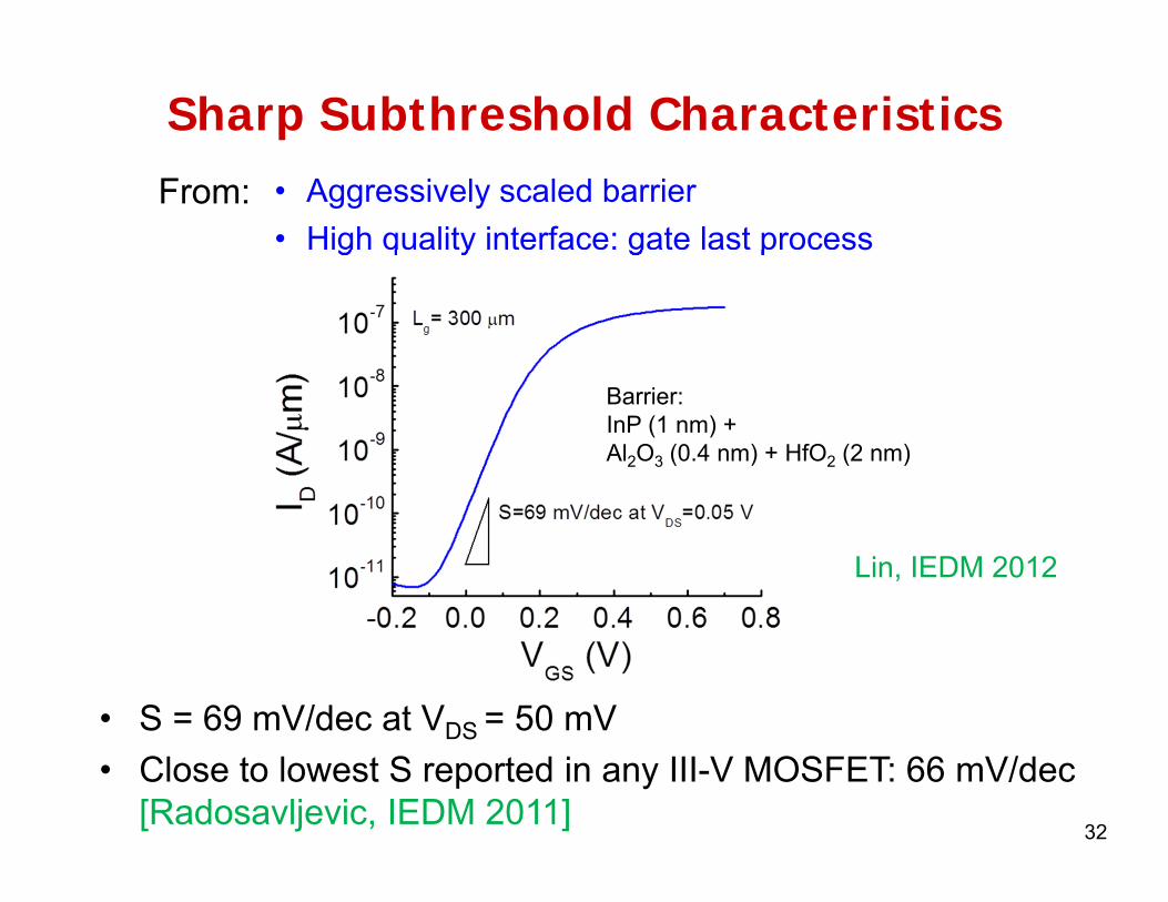
Sharp Subthreshold Characteristics
32
• S = 69 mV/dec at VDS = 50 mV• Close to lowest S reported in any III-V MOSFET: 66 mV/dec
[Radosavljevic, IEDM 2011]
• Aggressively scaled barrier• High quality interface: gate last process
Lin, IEDM 2012
Barrier:InP (1 nm) + Al2O3 (0.4 nm) + HfO2 (2 nm)
From:
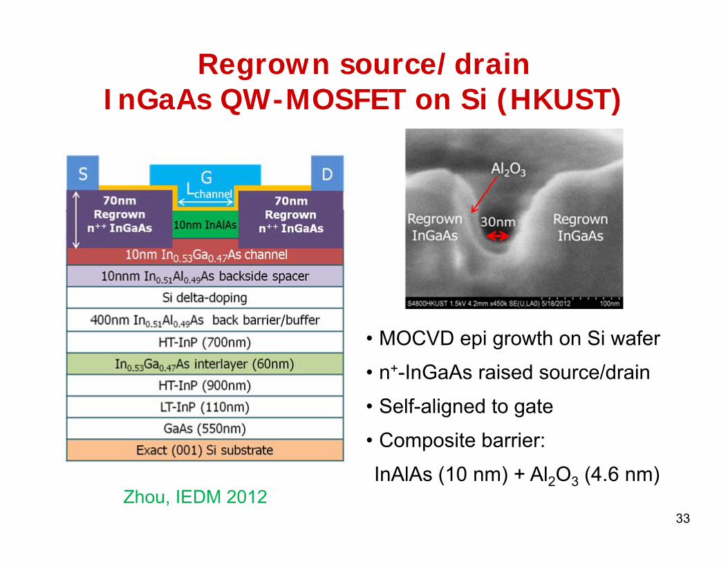
Regrown source/drain InGaAs QW-MOSFET on Si (HKUST)
33
• MOCVD epi growth on Si wafer
• n+-InGaAs raised source/drain
• Self-aligned to gate
• Composite barrier:
InAlAs (10 nm) + Al2O3 (4.6 nm)Zhou, IEDM 2012
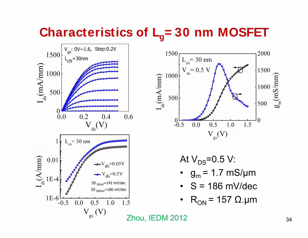
Characteristics of Lg=30 nm MOSFET
34
At VDS=0.5 V:• gm = 1.7 mS/µm• S = 186 mV/dec• RON = 157 Ω.µm
Zhou, IEDM 2012
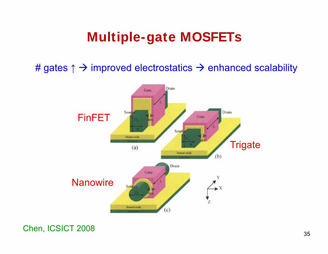
Multiple-gate MOSFETs
# gates ↑ improved electrostatics enhanced scalability
35
FinFET
Trigate
Nanowire
Chen, ICSICT 2008
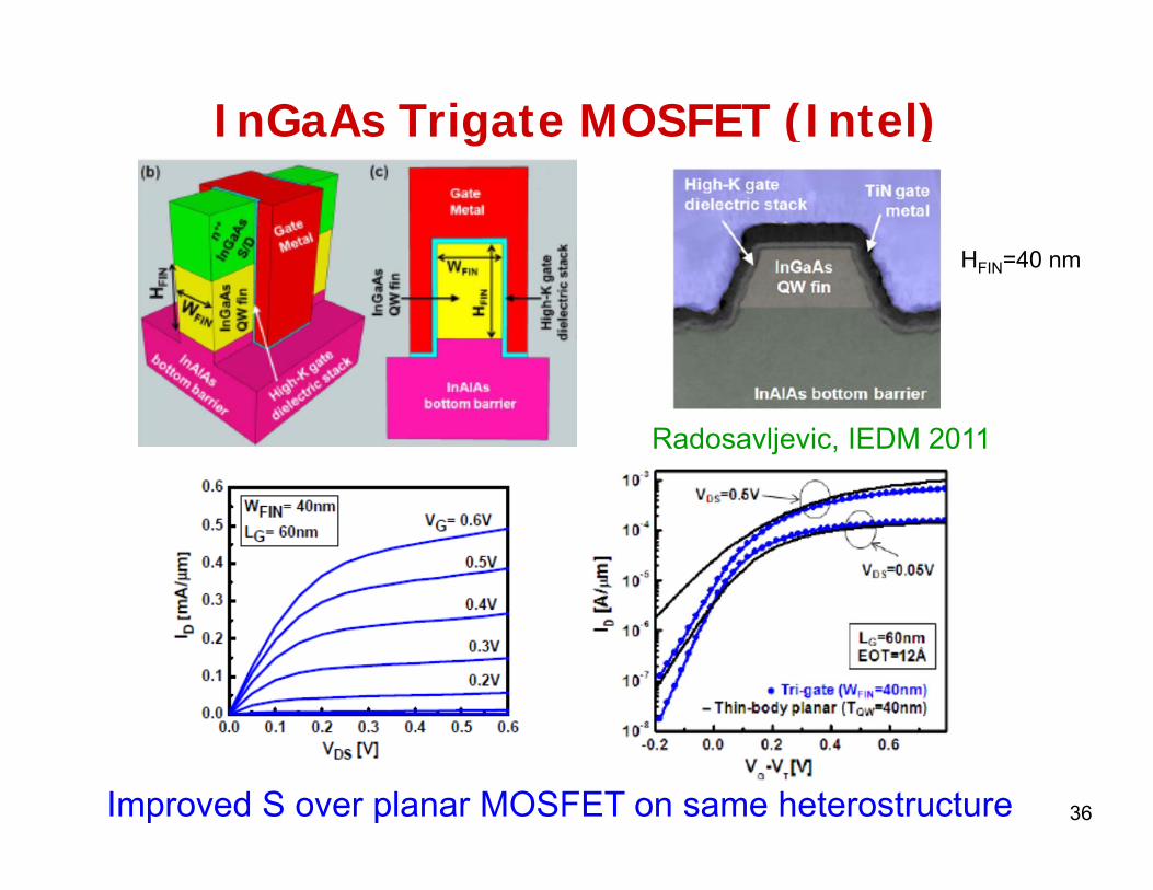
InGaAs Trigate MOSFET (Intel)
36Improved S over planar MOSFET on same heterostructure
Radosavljevic, IEDM 2011
HFIN=40 nm
D = 30 nm
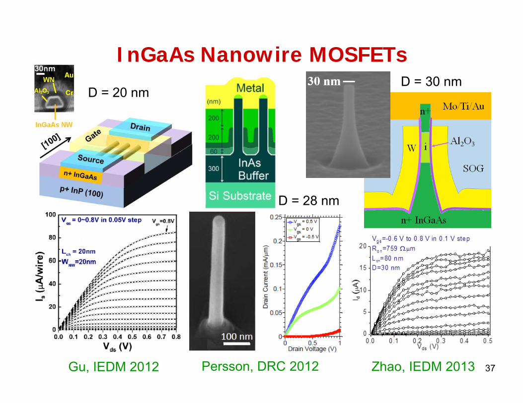
InGaAs Nanowire MOSFETs
37Gu, IEDM 2012
D = 20 nm
Zhao, IEDM 2013
D = 28 nm
Persson, DRC 2012
38
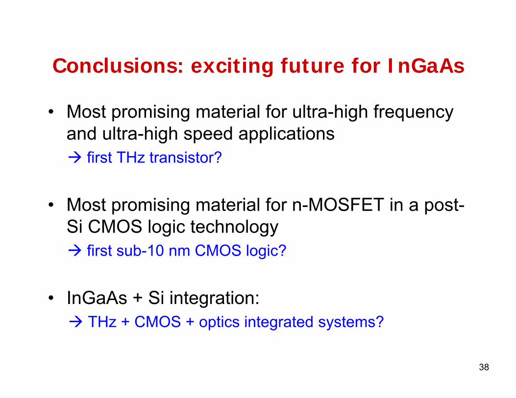
Conclusions: exciting future for InGaAs
• Most promising material for ultra-high frequency and ultra-high speed applications first THz transistor?
• Most promising material for n-MOSFET in a post-Si CMOS logic technology first sub-10 nm CMOS logic?
• InGaAs + Si integration: THz + CMOS + optics integrated systems?
Related Documents


![Subcycle Nonlinear Response of Doped 4H Silicon Carbide ......instance GaAs, Si, Ge, and InGaAs [18-23]. In line with its potential for high-power THz applications, the possibility](https://static.cupdf.com/doc/110x72/60df2e31b666e81ebd71dfd6/subcycle-nonlinear-response-of-doped-4h-silicon-carbide-instance-gaas-si.jpg)


