ARTICLE Received 6 Nov 2013 | Accepted 12 Mar 2014 | Published 3 Apr 2014 Nanomechanical cleavage of molybdenum disulphide atomic layers Dai-Ming Tang 1 , Dmitry G. Kvashnin 2,3 , Sina Najmaei 4 , Yoshio Bando 5 , Koji Kimoto 6 , Pekka Koskinen 7 , Pulickel M. Ajayan 4 , Boris I. Yakobson 4 , Pavel B. Sorokin 2,3,8 , Jun Lou 4 & Dmitri Golberg 5 The discovery of two-dimensional materials became possible due to the mechanical cleavage technique. Despite its simplicity, the as-cleaved materials demonstrated surprising macro- continuity, high crystalline quality and extraordinary mechanical and electrical properties that triggered global research interest. Here such cleavage processes and associated mechanical behaviours are investigated by a direct in situ transmission electron microscopy probing technique, using atomically thin molybdenum disulphide layers as a model material. Our technique demonstrates layer number selective cleavage, from a monolayer to double layer and up to 23 atomic layers. In situ observations combined with molecular dynamics simulations reveal unique layer-dependent bending behaviours, from spontaneous rippling (o5 atomic layers) to homogeneous curving (B 10 layers) and finally to kinking (20 or more layers), depending on the competition of strain energy and interfacial energy. DOI: 10.1038/ncomms4631 1 International Center for Young Scientists (ICYS), National Institute for Materials Science (NIMS), Namiki 1-1, Tsukuba 3050044, Japan. 2 National University of Science and Technology MISiS, 4 Leninskiy prospekt, Moscow 119049, Russian Federation. 3 Emanuel Institute of Biochemical Physics, 4 Kosigina Street, Moscow 119334, Russian Federation. 4 Department of Materials Science and NanoEngineering, Rice University, Houston, Texas 77005, USA. 5 World Premier International (WPI) Center for Materials Nanoarchitectonics (MANA), National Institute for Materials Science (NIMS), Namiki 1-1, Tsukuba 3050044, Japan. 6 Surface Physics and Structure Unit, National Institute for Materials Science (NIMS), Namiki 1-1, Tsukuba 3050044, Japan. 7 NanoScience Center, Department of Physics, University of Jyva ¨skyla ¨, Jyva ¨skyla ¨ FI-40014, Finland. 8 Technological Institute of Superhard and Novel Carbon Materials, 7a Centralnaya Street, Troitsk, Moscow 142190, Russian Federation. Correspondence and requests for materials should be addressed to J.L. (email: [email protected]) or to D.G. (email: [email protected]). NATURE COMMUNICATIONS | 5:3631 | DOI: 10.1038/ncomms4631 | www.nature.com/naturecommunications 1 & 2014 Macmillan Publishers Limited. All rights reserved.

Welcome message from author
This document is posted to help you gain knowledge. Please leave a comment to let me know what you think about it! Share it to your friends and learn new things together.
Transcript
ARTICLE
Received 6 Nov 2013 | Accepted 12 Mar 2014 | Published 3 Apr 2014
Nanomechanical cleavage of molybdenumdisulphide atomic layersDai-Ming Tang1, Dmitry G. Kvashnin2,3, Sina Najmaei4, Yoshio Bando5, Koji Kimoto6, Pekka Koskinen7,
Pulickel M. Ajayan4, Boris I. Yakobson4, Pavel B. Sorokin2,3,8, Jun Lou4 & Dmitri Golberg5
The discovery of two-dimensional materials became possible due to the mechanical cleavage
technique. Despite its simplicity, the as-cleaved materials demonstrated surprising macro-
continuity, high crystalline quality and extraordinary mechanical and electrical properties that
triggered global research interest. Here such cleavage processes and associated mechanical
behaviours are investigated by a direct in situ transmission electron microscopy probing
technique, using atomically thin molybdenum disulphide layers as a model material. Our
technique demonstrates layer number selective cleavage, from a monolayer to double layer
and up to 23 atomic layers. In situ observations combined with molecular dynamics
simulations reveal unique layer-dependent bending behaviours, from spontaneous rippling
(o5 atomic layers) to homogeneous curving (B 10 layers) and finally to kinking (20 or more
layers), depending on the competition of strain energy and interfacial energy.
DOI: 10.1038/ncomms4631
1 International Center for Young Scientists (ICYS), National Institute for Materials Science (NIMS), Namiki 1-1, Tsukuba 3050044, Japan. 2 National Universityof Science and Technology MISiS, 4 Leninskiy prospekt, Moscow 119049, Russian Federation. 3 Emanuel Institute of Biochemical Physics, 4 Kosigina Street,Moscow 119334, Russian Federation. 4 Department of Materials Science and NanoEngineering, Rice University, Houston, Texas 77005, USA.5 World Premier International (WPI) Center for Materials Nanoarchitectonics (MANA), National Institute for Materials Science (NIMS), Namiki 1-1, Tsukuba3050044, Japan. 6 Surface Physics and Structure Unit, National Institute for Materials Science (NIMS), Namiki 1-1, Tsukuba 3050044, Japan. 7 NanoScienceCenter, Department of Physics, University of Jyvaskyla, Jyvaskyla FI-40014, Finland. 8 Technological Institute of Superhard and Novel Carbon Materials,7a Centralnaya Street, Troitsk, Moscow 142190, Russian Federation. Correspondence and requests for materials should be addressed to J.L.(email: [email protected]) or to D.G. (email: [email protected]).
NATURE COMMUNICATIONS | 5:3631 | DOI: 10.1038/ncomms4631 | www.nature.com/naturecommunications 1
& 2014 Macmillan Publishers Limited. All rights reserved.
Mechanical cleavage technique, also known as theScotch-tape method, has resulted in the discovery oftwo-dimensional (2D) crystals. It is a rather crude
procedure, but, surprisingly, the produced samples demonstratedexcellent quality and performance1–7. The simplicity of the Scotchtape method has initiated a booming research on graphene andother 2D materials. A rich family of such materials has beendiscovered, such as boron nitride (BN), molybdenum disulphide(MoS2), niobium diselenide (NbSe2) and Bi2Sr2CaCu2Ox (ref. 7).However, the atomic processes of the micromechanical cleavageare still poorly understood. How will the atomically thin filmsbehave during the cleavage and under the large bendingconditions? Will they bend as a whole plate or will theinterlayer sliding occur? Will they lose structural stability undersevere bending deformation? These concerns call for a directinvestigation into the initial stage of the mechanical cleavageprocess.
One particularly promising application for the 2D crystals isflexible electronics, because of their strong in-plane bondingand high flexibility8–13. MoS2 atomic layers are competitivecandidates with suitable electronic structures14–16. Bulk MoS2 is alayered semiconductor with an indirect band gap of B1.29 eV.However, recently it has been demonstrated that MoS2
monolayers have direct band gaps of B1.8 eV with a strongphotoluminescence14,15. In addition, the MoS2-based field effecttransistors have shown outstanding performances with highON/OFF ratios6. Moreover, high-performance MoS2 thin-filmtransistors and gas sensors have been fabricated on flexiblesubstrates10–13. It is important to study the 2D-MoS2 mechanicalproperties for their reliable applications in flexible electronicdevices. Bertolazzi et al.5 reported fracture strength as high as23 GPa at an effective strain of 11%, indicating that the 2D-MoS2
could be almost defect free. The elastic properties were studiedby Castellanos-Gomez et al.16 who reported extraordinary highYoung’s modulus E¼ 0.33±0.07 TPa for the freely suspended5–25 layers thick MoS2 nanosheets. However, despite the above-mentioned notable progress, there have been no reports regardingthe mechanical behaviour of the MoS2 atomic layers underbending and folding conditions, although this ultimatelydetermines the mechanical reliability of the flexible electronicdevices made of such 2D semiconductors.
In this work, we design an in situ transmission electronmicroscopy (TEM) probing technique17–20 to investigate theinitial stages of the 2D crystal cleavage, which is defined here asthe ‘nanomechanical cleavage’, using MoS2 atomic layers as amodel material. By precisely manipulating an ultra-sharp metalprobe to contact the pre-existing crystalline steps of the MoS2
single crystals, atomically thin flakes are delicately peeled off,selectively ranging from a single, double to more than 20 atomiclayers. The mechanical behaviours of the MoS2 atomic layersduring cleavage, bending and folding processes are investigatedin situ. It is found that the mechanical behaviours are stronglydependent on the number of layers. Combination of in situTEM and molecular dynamic (MD) simulations allows us tothoroughly investigate a transformation of bending behaviourfrom homogeneous curving to kinking.
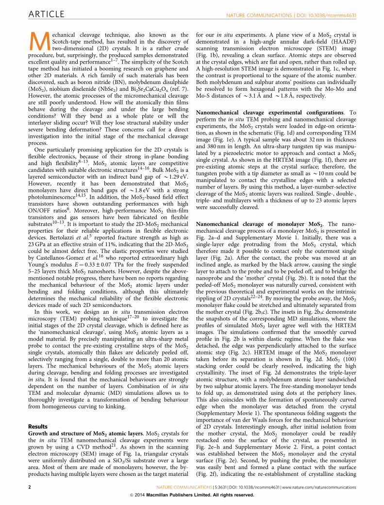
ResultsGrowth and structure of MoS2 atomic layers. MoS2 crystals forthe in situ TEM nanomechanical cleavage experiments weregrown by using a CVD method21. As shown in the scanningelectron microscopy (SEM) image of Fig. 1a, triangular crystalswere uniformly distributed on a SiO2/Si substrate over a largearea. Most of them are made of monolayers; however, the by-products having multiple layers were chosen as the target material
for our in situ experiments. A plane view of a MoS2 crystal isdemonstrated in a high-angle annular dark-field (HAADF)scanning transmission electron microscope (STEM) image(Fig. 1b), revealing a clean surface. Atomic steps are observedat the crystal edges, which are flat and open, rather than rolled up.A high-resolution STEM image is demonstrated in Fig. 1c, wherethe contrast is proportional to the square of the atomic number.Both molybdenum and sulphur atoms’ positions can individuallybe resolved to form hexagonal patterns with the Mo-Mo andMo-S distances of B3.1 Å and B1.8 Å, respectively.
Nanomechanical cleavage experimental configurations. Toperform the in situ TEM probing and nanomechanical cleavageexperiments, the MoS2 crystals were loaded in edge-on orienta-tion, as shown in the schematic (Fig. 1d) and corresponding TEMimage (Fig. 1e). A typical sample was about 32 nm in thicknessand 380 nm in length. An ultra-sharp tungsten tip was manipu-lated by a piezoelectric motor to approach and contact a MoS2
single crystal. As shown in the HRTEM image (Fig. 1f), there arepre-existing atomic steps at the crystal surface; therefore, thetungsten probe with a tip diameter as small as B10 nm could bemanipulated to contact the crystalline edges with a selectednumber of layers. By using this method, a layer-number-selectivecleavage of the MoS2 atomic layers was realized. Single-, double-,triple- and multilayers with a thickness of up to 23 atomic layerswere successfully cleaved.
Nanomechanical cleavage of monolayer MoS2. The nano-mechanical cleavage process of a monolayer MoS2 is presented inFig. 2a–d and Supplementary Movie 1. Initially, there was asingle-layer edge protruding from the MoS2 crystal, whichtherefore made it possible to contact only the outermost singlelayer (Fig. 2a). After the contact, the probe was moved at aninclined angle, as marked by the black arrow, causing the singlelayer to attach to the probe and to be peeled off, and to bridge thenanoprobe and the ‘mother’ crystal (Fig. 2b). It is noted that thepeeled-off MoS2 monolayer was naturally curved, consistent withthe previous theoretical and experimental works on the intrinsicrippling of 2D crystals22–24. By moving the probe away, the MoS2
monolayer flake could be stretched and ultimately separated fromthe mother crystal (Fig. 2b,c). The insets in Fig. 2b,c demonstratethe snapshots of the corresponding MD simulations, where theprofiles of simulated MoS2 layer agree well with the HRTEMimages. The simulations confirmed that the smoothly curvedprofile in Fig. 2b is within elastic regime. When the flake wasdetached, the edge was perpendicularly attached to the surfaceatomic step (Fig. 2c). HRTEM image of the MoS2 monolayertaken before its separation is shown in Fig. 2d. MoS2 (100)stacking order could be clearly resolved, indicating the highcrystallinity. The inset of Fig. 2d demonstrates the triple-layeratomic structure, with a molybdenum atomic layer sandwichedby two sulphur atomic layers. The free-standing monolayer tendsto fold up, as demonstrated using dots at the periphery lines.This also coincides with the formation of spontaneously curvededge when the monolayer was detached from the crystal(Supplementary Movie 1). The spontaneous folding suggests theimportance of van der Waals forces for the mechanical behaviourof 2D crystals. Interestingly enough, after initial isolation fromthe mother crystal, the MoS2 monolayer could be readilyrestacked onto the surface of the crystal, as presented inFig. 2e–h and Supplementary Movie 2. First, a point contactwas established between the MoS2 monolayer and the crystalsurface (Fig. 2e). Second, by pushing the probe, the monolayerwas easily bent and formed a plane contact with the surface(Fig. 2f), indicating the re-establishment of crystalline stacking
ARTICLE NATURE COMMUNICATIONS | DOI: 10.1038/ncomms4631
2 NATURE COMMUNICATIONS | 5:3631 | DOI: 10.1038/ncomms4631 | www.nature.com/naturecommunications
& 2014 Macmillan Publishers Limited. All rights reserved.
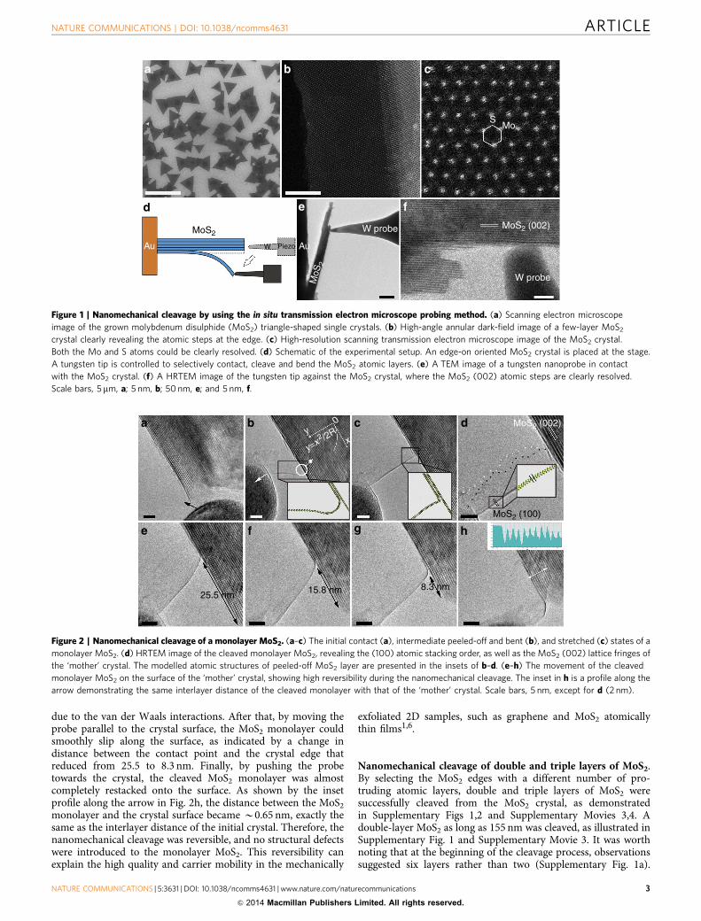
due to the van der Waals interactions. After that, by moving theprobe parallel to the crystal surface, the MoS2 monolayer couldsmoothly slip along the surface, as indicated by a change indistance between the contact point and the crystal edge thatreduced from 25.5 to 8.3 nm. Finally, by pushing the probetowards the crystal, the cleaved MoS2 monolayer was almostcompletely restacked onto the surface. As shown by the insetprofile along the arrow in Fig. 2h, the distance between the MoS2
monolayer and the crystal surface became B0.65 nm, exactly thesame as the interlayer distance of the initial crystal. Therefore, thenanomechanical cleavage was reversible, and no structural defectswere introduced to the monolayer MoS2. This reversibility canexplain the high quality and carrier mobility in the mechanically
exfoliated 2D samples, such as graphene and MoS2 atomicallythin films1,6.
Nanomechanical cleavage of double and triple layers of MoS2.By selecting the MoS2 edges with a different number of pro-truding atomic layers, double and triple layers of MoS2 weresuccessfully cleaved from the MoS2 crystal, as demonstratedin Supplementary Figs 1,2 and Supplementary Movies 3,4. Adouble-layer MoS2 as long as 155 nm was cleaved, as illustrated inSupplementary Fig. 1 and Supplementary Movie 3. It was worthnoting that at the beginning of the cleavage process, observationssuggested six layers rather than two (Supplementary Fig. 1a).
SMo
MoS2 (002)
W probe
W probe
AuPiezo
MoS
2
W
MoS2
Au
Figure 1 | Nanomechanical cleavage by using the in situ transmission electron microscope probing method. (a) Scanning electron microscope
image of the grown molybdenum disulphide (MoS2) triangle-shaped single crystals. (b) High-angle annular dark-field image of a few-layer MoS2
crystal clearly revealing the atomic steps at the edge. (c) High-resolution scanning transmission electron microscope image of the MoS2 crystal.
Both the Mo and S atoms could be clearly resolved. (d) Schematic of the experimental setup. An edge-on oriented MoS2 crystal is placed at the stage.
A tungsten tip is controlled to selectively contact, cleave and bend the MoS2 atomic layers. (e) A TEM image of a tungsten nanoprobe in contact
with the MoS2 crystal. (f) A HRTEM image of the tungsten tip against the MoS2 crystal, where the MoS2 (002) atomic steps are clearly resolved.
Scale bars, 5mm, a; 5 nm, b; 50 nm, e; and 5 nm, f.
0y
xy=x2 /2R
25.5 nm 15.8 nm 8.3 nm
MoS2 (100)
MoS2 (002)
Figure 2 | Nanomechanical cleavage of a monolayer MoS2. (a–c) The initial contact (a), intermediate peeled-off and bent (b), and stretched (c) states of a
monolayer MoS2. (d) HRTEM image of the cleaved monolayer MoS2, revealing the (100) atomic stacking order, as well as the MoS2 (002) lattice fringes of
the ‘mother’ crystal. The modelled atomic structures of peeled-off MoS2 layer are presented in the insets of b–d. (e–h) The movement of the cleaved
monolayer MoS2 on the surface of the ‘mother’ crystal, showing high reversibility during the nanomechanical cleavage. The inset in h is a profile along the
arrow demonstrating the same interlayer distance of the cleaved monolayer with that of the ‘mother’ crystal. Scale bars, 5 nm, except for d (2 nm).
NATURE COMMUNICATIONS | DOI: 10.1038/ncomms4631 ARTICLE
NATURE COMMUNICATIONS | 5:3631 | DOI: 10.1038/ncomms4631 | www.nature.com/naturecommunications 3
& 2014 Macmillan Publishers Limited. All rights reserved.
This is because of the mechanical contact with the probe, whichled to the edge bending, rolling and crumpling. Under stretching,the crumpled MoS2 sheet became flat, and a double layer latticebecame apparent (Supplementary Fig. 1d). Similar process andability to recover from severe deformations were demonstratedfor a triple-layer MoS2 (Supplementary Fig. 2). The extraordinaryability to restore deformed structures demonstrates the highflexibility of the MoS2 atomic layers, which is crucial for theirapplications in flexible electronics. The minimum bending radiusfor the inner layer of double and triple MoS2 was about 3.0 nmand 3.1 nm, respectively. A common feature during bending wasspontaneous rippling (Supplementary Figs 1c and 2d), which wasattributed to thermal fluctuations22–24.
Nanomechanical cleavage of 5- and 11-layer MoS2. In ourexperiments, it was found that the mechanical behaviours of theMoS2 atomic layers had been closely dependent on the number oflayers (thickness) of the flakes. In the following section, themechanical behaviour of comparatively thick MoS2 stacks isdiscussed. The number of layers ranges from 5 to 11 in thecorresponding experiments. In contrast to the relaxed ripples andfolded-up configurations in the mono-, double- and triple-layerMoS2, such flakes were more rigid, as demonstrated by thestraight profile during the bending process (Fig. 3, SupplementaryFig. 3, and Supplementary Movies 5,6). This change is plausible,because a thicker membrane with a larger bending stiffness willhave smaller displacements due to thermal fluctuations accordingto the relation oh24p TL2/k, where L is the size of the sampleand k is the bending rigidity25,26. It is worth noting that, for the5-layer MoS2, when the flake was released from the probe, it keptthe bent configuration and was attached to the surface of the‘mother crystal’, again indicating the importance of van derWaals forces for the stability and mechanical behaviours of theultrathin crystals.
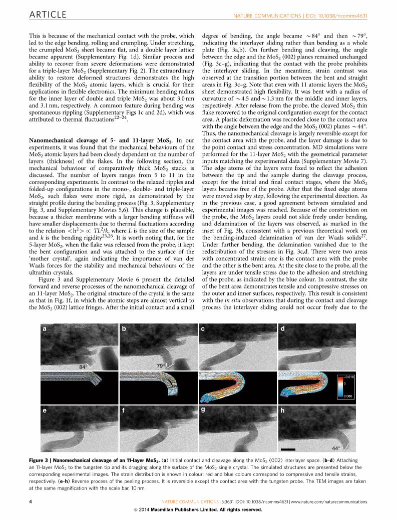
Figure 3 and Supplementary Movie 6 present the detailedforward and reverse processes of the nanomechanical cleavage ofan 11-layer MoS2. The original structure of the crystal is the sameas that in Fig. 1f, in which the atomic steps are almost vertical tothe MoS2 (002) lattice fringes. After the initial contact and a small
degree of bending, the angle became B84� and then B79�,indicating the interlayer sliding rather than bending as a wholeplate (Fig. 3a,b). On further bending and cleaving, the anglebetween the edge and the MoS2 (002) planes remained unchanged(Fig. 3c–g), indicating that the contact with the probe prohibitsthe interlayer sliding. In the meantime, strain contrast wasobserved at the transition portion between the bent and straightareas in Fig. 3c–g. Note that even with 11 atomic layers the MoS2
sheet demonstrated high flexibility. It was bent with a radius ofcurvature of B4.5 andB1.3 nm for the middle and inner layers,respectively. After release from the probe, the cleaved MoS2 thinflake recovered to the original configuration except for the contactarea. A plastic deformation was recorded close to the contact areawith the angle between the edge and the MoS2 (002) planes B44�.Thus, the nanomechanical cleavage is largely reversible except forthe contact area with the probe, and the layer damage is due tothe point contact and stress concentration. MD simulations wereperformed for the 11-layer MoS2 with the geometrical parameterinputs matching the experimental data (Supplementary Movie 7).The edge atoms of the layers were fixed to reflect the adhesionbetween the tip and the sample during the cleavage process,except for the initial and final contact stages, where the MoS2
layers became free of the probe. After that the fixed edge atomswere moved step by step, following the experimental direction. Asin the previous case, a good agreement between simulated andexperimental images was reached. Because of the constriction onthe probe, the MoS2 layers could not slide freely under bending,and delamination of the layers was observed, as marked in theinset of Fig. 3b, consistent with a previous theoretical work onthe bending-induced delamination of van der Waals solids27.Under further bending, the delamination vanished due to theredistribution of the stresses in Fig. 3c,d. There were two areaswith concentrated strain: one is the contact area with the probeand the other is the bent area. At the site close to the probe, all thelayers are under tensile stress due to the adhesion and stretchingof the probe, as indicated by the blue colour. In contrast, the siteof the bent area demonstrates tensile and compressive stresses onthe outer and inner surfaces, respectively. This result is consistentwith the in situ observations that during the contact and cleavageprocess the interlayer sliding could not occur freely due to the
84° 79°
44°
–0.016
0
0.086
Figure 3 | Nanomechanical cleavage of an 11-layer MoS2. (a) Initial contact and cleavage along the MoS2 (002) interlayer space. (b–d) Attaching
an 11-layer MoS2 to the tungsten tip and its dragging along the surface of the MoS2 single crystal. The simulated structures are presented below the
corresponding experimental images. The strain distribution is shown in colour: red and blue colours correspond to compressive and tensile strains,
respectively. (e–h) Reverse process of the peeling process. It is reversible except the contact area with the tungsten probe. The TEM images are taken
at the same magnification with the scale bar, 10 nm.
ARTICLE NATURE COMMUNICATIONS | DOI: 10.1038/ncomms4631
4 NATURE COMMUNICATIONS | 5:3631 | DOI: 10.1038/ncomms4631 | www.nature.com/naturecommunications
& 2014 Macmillan Publishers Limited. All rights reserved.
constriction of the MoS2-probe interface. Therefore, while thefree standing MoS2 atomic crystals can easily slide duringbending, the actual deformation process also depends on theboundary conditions.
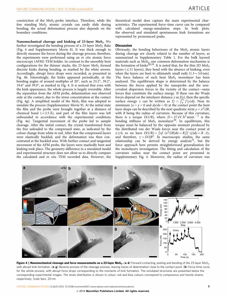
Nanomechanical cleavage and kinking of 23-layer MoS2. Wefurther investigated the bending process of a 23-layer MoS2 flake(Fig. 4 and Supplementary Movie 8). It was thick enough todirectly measure the forces during the cleavage process; therefore,the experiments were performed using an in situ atomic forcemicroscopy (AFM)-TEM holder. In contrast to the smoothly bentconfigurations for the thinner stacks, the 23-layer MoS2 formeddiscrete kinks during bending, as marked by the white arrows.Accordingly, abrupt force drops were recorded, as presented inFig. 4h. Interestingly, the kinks appeared periodically, at thebending angles of around multiples of 20�, such as 23.2�, 39.2�,19.6� and 39.0�, as marked in Fig. 4. It is noticed that even withthe kink appearance, the whole process is largely reversible. Afterthe separation from the AFM probe, delamination was observedonly at the contact, due to the stress concentration at the contact(Fig. 4g). A simplified model of the MoS2 film was adopted tosimulate the process (Supplementary Movie 9). At the initial statethe film and the probe were brought together at a distance ofchemical bond (o2.5 Å), and part of the film layers was leftunbounded in accordance with the experimental conditions(Fig. 4a). Tangential movement of the probe led to samplecleavage. After the initial contact, the crystal transformed fromthe free unloaded to the compressed state, as indicated by thecolour change from white to red. After that the compressed layerswere elastically buckled, and the deformation was then con-centrated at the buckled area. With further contact and tangentialmovement of the AFM probe, the layers were markedly bent andkinking took place. The geometry difference in a simulated modeland experimental structure does not allow us to directly comparethe calculated and in situ TEM recorded data. However, the
theoretical model does capture the main experimental char-acteristics. The experimental force–time curve can be comparedwith calculated energy-simulation steps. In both plots,the observed and simulated spontaneous kink formations arerepresented by pronounced peaks.
DiscussionObviously, the bending behaviours of the MoS2 atomic layersduring cleavage are closely related to the number of layers, assummarized in Supplementary Table 1. For the bulk layeredmaterials such as MoS2, one common deformation mechanism isthe formation of kinks28,29. It is noted that, for the thin 2D MoS2
layers (r11 layers), they bend with the absence of kinking, evenwhen the layers are bent to ultimately small radii (1.3B3.0 nm).The force balance of such bent MoS2 monolayer has beenanalysed. The equilibrium shape is determined by the balancebetween the forces applied by the nanoprobe and the non-covalent dispersion forces in the vicinity of the contact—sameforces that constitute the surface energy. If these van der Waalsforces depend on the interlayer distance y as f(y), then the specificsurface energy g can be written as 2g ¼
R10 f ðyÞdy. Near its
minimum (x¼ y¼ 0 and dy/dx¼ 0) at the contact point the bentlayer shape can be described by the next quadratic term y¼ x2/2R,with R being the radius of curvature. Because of this curvature,there is a torque D(1/R), where D¼ 27 eV Å2 atom� 1 is thebending stiffness of MoS2 monolayer30. In equilibrium, thistorque must be balanced by the opposite moment produced bythe distributed van der Waals forces near the contact point atxZ0, so we have D(1/R)¼
Rxf (x2/2R)dx¼R
Rf (y)dy¼R � 2g,
and therefore, g¼D/2R2. In macroscopic studies, the samerelationship can be derived by energy analysis31, but theforce approach here permits straightforward generalization forthe monolayers investigation. The fitting and calculation of thecurvature radius near the contact point are presented inSupplementary Fig. 4. Moreover, the radius of curvature was
MoS2
Kink
Kink
KinkAu
Kink
1401201008060
Ene
rgy
(eV
)F
orce
(nN
)
40200
250
200
150
100
50
00 50 100 150 200
Time (s)
0 1,000 2,000Step
Kinks
3,000 4,000
AFM
∼23.2°
∼19.6°
∼39.0°
∼39.2°
−0.016
0
0.086
Figure 4 | Nanomechanical cleavage and force measurements on a 23-layer MoS2. (a–d) Forward contacting, peeling and bending of the 23-layer MoS2,
with abrupt kink formation. (e–g) Reverse process of the cleavage process, leaving traces of delamination close to the contact point. (h) Force–time curve
for the whole process, with abrupt force drops corresponding to the moments of kink formation. The simulated structures are presented below the
corresponding experimental images. The strain distribution is shown in colour: red and blue colours correspond to compressive and tensile strains,
respectively. Scale bars, 20 nm.
NATURE COMMUNICATIONS | DOI: 10.1038/ncomms4631 ARTICLE
NATURE COMMUNICATIONS | 5:3631 | DOI: 10.1038/ncomms4631 | www.nature.com/naturecommunications 5
& 2014 Macmillan Publishers Limited. All rights reserved.
calculated to be B1.5 nm. Accordingly, the specific surface energyof MoS2 monolayer is calculated to be B0.06 eV atom� 1
or B0.11 N m� 1. Determination of the surface energy isfundamentally important for various processes, such as catalysisand lubrication. Previously, the specific surface energy of MoS2
has mainly been investigated by theoretical calculations. In early
publications, comparatively high values such as 0.26 and0.28 N m� 1 were reported32,33. However, the specific surfaceenergy of MoS2 was derived from liquid exfoliation processes34,35
to be B0.07 N m� 1. Recently, a more accurate random-phaseapproximation (RPA) method was adopted for the calculations ofthe binding energy of the van der Waals bonding in layeredcompounds34. Interlayer binding energies for a large number oflayered compounds, including MoS2, were calculated to bearound 20 meV � 2 (B0.32 N m� 1), with the specific surfaceenergy being half of that value (B0.16 N m� 1)34. Thus, ourdirectly measured value is reasonably consistent with the mostaccurate RPA calculations currently available.
For the multi-layer MoS2 flakes, an important issue is whetherthe layers slide or the sample will bend as a plate. Shen et al.26
reported that sliding would dominate the bending for graphenenanoribbons, due to the low interlayer shear modulus. However,Koskinen27 and Nikiforov et al.35 found that when the edge ofgraphene nanoribbons was fixed, kinks and delamination becamethe major deformation mechanism. In our experiments, it wasfound that, while the free standing MoS2 crystals are easy to slide,the interlayer sliding could be restricted by the interaction withthe probes. The easy sliding could be understood by the low shearstrength, which has been reported to be only around 0.1 GPa(refs 36–38). With a given maximum shear stress (tmax), thethreshold bending angle for sliding can be calculated simply byapplying the strength theory of materials39 as ymax ¼ 4L2tmax
EN2d2 ,where L is the length, E is the Young’s modulus, N is the layernumber and d is the interlayer distance. Therefore, the thresholdangle is proportional to the square of length and inverselyproportional to the square of layer number, as demonstrated inSupplementary Fig. 5. For example, for an MoS2 sheet with alength of 10 nm and five layers in thickness, the threshold anglewould be as small as B0.7�, which can explain the easy slidingduring bending. It is also seen that when the length of the 2Dcrystal becomes larger it is more difficult to slide, which canexplain why buckling rather than interlayer sliding became themajor mechanism for bending the long BN and graphenenanoribbons with a length around 1 mm (ref. 35). Because ofeasy interlayer sliding, the atomic layers bend mostlyindependently, which is the reason for the minimum radius(corresponding to the maximum bending) to be non-related tothe number of layers before the kinking mechanism comes intoeffect. The regarded 2D crystals might be bent to a radius as smallas B1.3 nm, showing that they are mechanically reliablecandidates for future flexible electronic devices.
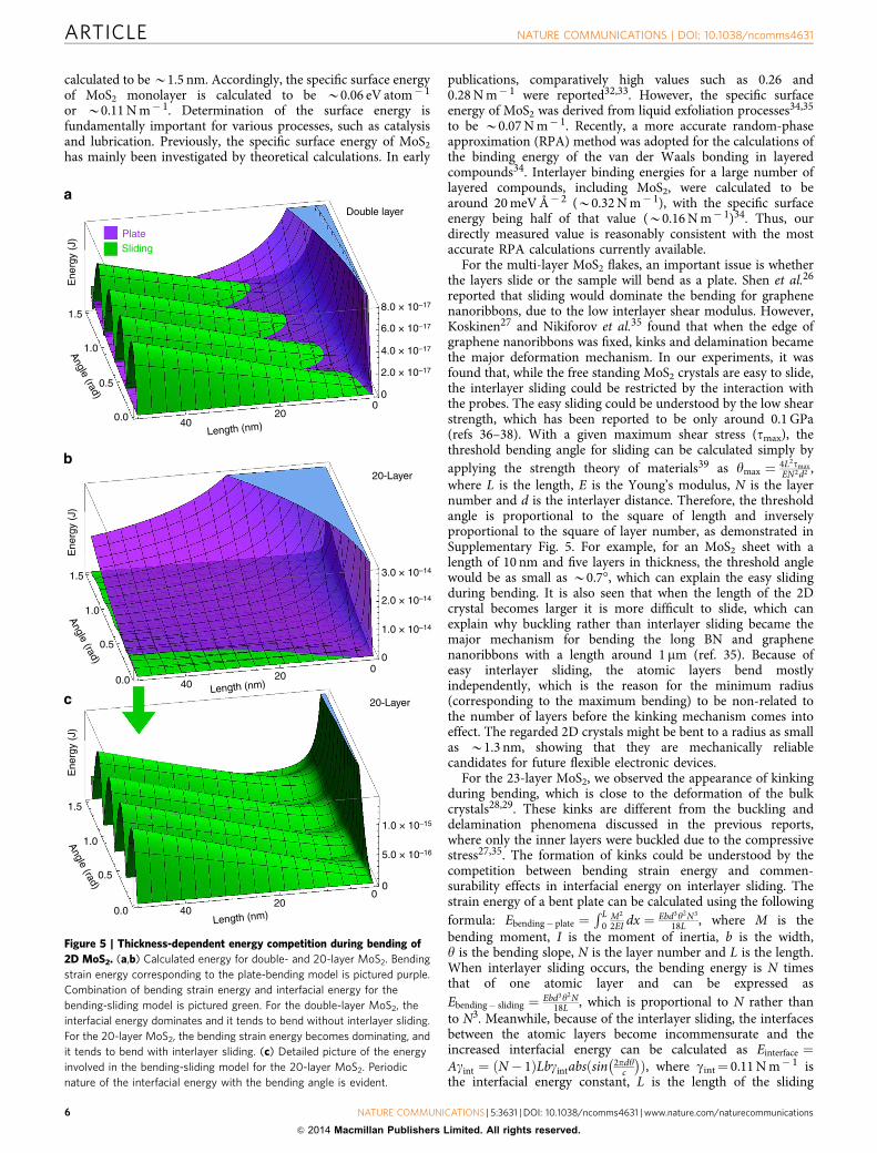
For the 23-layer MoS2, we observed the appearance of kinkingduring bending, which is close to the deformation of the bulkcrystals28,29. These kinks are different from the buckling anddelamination phenomena discussed in the previous reports,where only the inner layers were buckled due to the compressivestress27,35. The formation of kinks could be understood by thecompetition between bending strain energy and commen-surability effects in interfacial energy on interlayer sliding. Thestrain energy of a bent plate can be calculated using the followingformula: Ebending� plate ¼
R L0
M2
2EI dx ¼ Ebd3y2N3
18L , where M is thebending moment, I is the moment of inertia, b is the width,y is the bending slope, N is the layer number and L is the length.When interlayer sliding occurs, the bending energy is N timesthat of one atomic layer and can be expressed asEbending� sliding ¼ Ebd3y2N
18L , which is proportional to N rather thanto N3. Meanwhile, because of the interlayer sliding, the interfacesbetween the atomic layers become incommensurate and theincreased interfacial energy can be calculated as Einterface ¼Agint ¼ N � 1ð ÞLbgintabsðsin 2pdy
c
� �Þ, where gint¼ 0.11 N m� 1 is
the interfacial energy constant, L is the length of the sliding
Plate
Ene
rgy
(J)
Ene
rgy
(J)
Ene
rgy
(J)
1.5
Double layer
20-Layer
8.0 × 10⁻¹⁷
6.0 × 10⁻¹⁷
4.0 × 10⁻¹⁷
2.0 × 10⁻¹⁷
0
1.0
0.5
0.0 4020
0
Length (nm)
Length (nm)
Length (nm)
Angle (rad)
Sliding
1.5
1.0
0.5
0.0
Angle (rad)
1.5
1.0
0.5
0.0
Angle (rad)
4020
0
4020
00
0
3.0 × 10⁻¹⁴
2.0 × 10⁻¹⁴
1.0 × 10⁻¹⁴
20-Layer
5.0 × 10⁻¹⁶
1.0 × 10⁻¹⁵
Figure 5 | Thickness-dependent energy competition during bending of
2D MoS2. (a,b) Calculated energy for double- and 20-layer MoS2. Bending
strain energy corresponding to the plate-bending model is pictured purple.
Combination of bending strain energy and interfacial energy for the
bending-sliding model is pictured green. For the double-layer MoS2, the
interfacial energy dominates and it tends to bend without interlayer sliding.
For the 20-layer MoS2, the bending strain energy becomes dominating, and
it tends to bend with interlayer sliding. (c) Detailed picture of the energy
involved in the bending-sliding model for the 20-layer MoS2. Periodic
nature of the interfacial energy with the bending angle is evident.
ARTICLE NATURE COMMUNICATIONS | DOI: 10.1038/ncomms4631
6 NATURE COMMUNICATIONS | 5:3631 | DOI: 10.1038/ncomms4631 | www.nature.com/naturecommunications
& 2014 Macmillan Publishers Limited. All rights reserved.
interface and c is the lattice constant along the sliding direction.It is reasonable to assume that the interfacial energy is a periodicfunction of the interlayer sliding distance40,41. Figure 5demonstrates the calculated energy for double-, and 20-layerMoS2, where bending strain energy of the plate-bending model ispictured purple, and the combination of bending strain energyand interfacial energy related to the bending-sliding model ispictured green. For the double-layer MoS2, the interfacial energydominates and it tends to bend without sliding (Fig. 5a). Inconstrast, for the 20 layer-MoS2, the bending strain energybecomes dominating, and it tends to bend with interlayer sliding(Fig. 5b). Figure 5c presents the detailed feature of the energyinvolved in the bending-sliding model for the 20-layer MoS2.Clearly, the interfacial energy is a periodic function of thebending slope. Therefore, for the thick MoS2 flakes, during thesliding, when the interlayer sliding distance equals to the latticeconstant or any other periodic distance along the slidingdirection, the interfacial energy will show local minima. Whenthe energy ‘valleys’ are met, abrupt force drop can be expected,which reflects the formation of kinks. It is noted that the period isaround 0.36 rad (B20.6�), which is well consistent with ourexperimental observations.
In conclusion, we developed an in situ TEM probing techniquefor direct investigation of the nanomechanical cleavage of 2Dcrystals. MoS2 atomic layers were successfully cleaved from asingle crystal with the layer number predetermined by the precisemanipulation with an ultra-sharp probe. It was demonstrated thatsuch cleavage is highly reversible. In addition, combining thein situ experiments with the MD simulations, the thickness-dependent mechanical behaviours were revealed. The featuringbending kinetics transformed from homogeneous curving andrippling (o5 atomic layers) to interlayer sliding (B10 layers) andto kinking (B20 or more atomic layers).
MethodsGrowth and characterization. The MoS2 atomic layers were synthesized on aSiO2/Si substrate by a vapour phase growth at 850 �C, using MoO3 nanoribbonsand pure sulphur as the precursors and reactants, respectively21. The crystallinestructures of the MoS2 atomic layers were characterized by TEM/STEM. The TEMsamples were prepared by transferring the grown samples onto the TEM grids bydirect contacting, so that the samples were free of contamination. The high-resolution TEM/STEM characterization was carried out on a FEI Titan3 (Cube)microscope, equipped with a monochromator and Cs-correctors for probe-formingand imaging at an accelerating voltage of 300 kV in a HAADF imaging mode.
In situ TEM probing experiments. The in situ TEM probing experiments weremainly conducted using a scanning tunnelling microscope (STM)-TEM platform(‘Nanofactory Instruments AB’) in a HRTEM (JEM-3100FEF) with an acceleratingvoltage of 300 kV equipped with an OMEGA-type energy filter. Ultra-sharptungsten probes (B10 nm tip diameter) were produced by electrochemical etching.MoS2 single crystals were loaded on the edge of a gold wire with an edge-onorientation, and the tungsten tip movements were controlled by a piezoelectricmotor to approach and selectively contact the atomic edge steps. After that, thetungsten tip was moved backwards to start the nanomechanical cleavage of theMoS2 atomic layers. Bending deformation was then initiated by pushing thetungsten tip towards and along the edge of the MoS2 crystal. The in situ forcemeasurements were carried out by using AFM-TEM holder (‘NanofactoryInstruments AB’). The whole process was video recorded in real time by acharge-coupled device (CCD) camera.
Simulation methods. MD simulations were performed using the reactiveempirical bond-order and Lennard-Jones potentials implemented into theLarge-scale Atomic/Molecular Massively Parallel Simulator (LAMMPS) simulationpackage42. The Mo-S potential was parameterized to match density functionaltheory calculations of Mo, S and Mo-S structures43. The parameterization wassuccessfully applied in the investigation of the mechanical properties of crystallineMoS2 by the indentation method44 and in the studies of behaviour of MoS2
multilayered nanotubes in extreme pressure conditions45. This technique is perfectto describe structural and mechanical properties of the Mo-S systems consisting ofa large number of atoms (4104). The MoS2 systems were modelled as clusters witha length of B40 nm (for mono- and 11- layer structures containing 1,400 and13,300 atoms, respectively) and B100 nm (for a 23-layer structure containing
19,500 atoms). In the case of mono- and 11-layer samples, the atoms on the end ofthe upper layers were fixed imitating the tip and moved along the directioncorresponding to the experiment with a displacement step equal to 0.1 Å. In thecase of 23-layer sample, for the imitation of the adhesion between the bottom edgeof AFM tip and the sample, the MoS2 monolayer of finite length was fixed andmoved directly to the sample along the direction corresponding to the experimentswith a displacement step equal to 0.1 Å.
References1. Novoselov, K. S. et al. Electric field effect in atomically thin carbon films.
Science 306, 666–669 (2004).2. Novoselov, K. S. et al. Two-dimensional gas of massless dirac fermions in
graphene. Nature 438, 197–200 (2005).3. Zhang, Y. B., Tan, Y. W., Stormer, H. L. & Kim, P. Experimental observation of
the quantum Hall effect and Berry’s phase in graphene. Nature 438, 201–204(2005).
4. Lee, C., Wei, X., Kysar, J. W. & Hone, J. Measurement of the elasticproperties and intrinsic strength of monolayer graphene. Science 321,385–388 (2008).
5. Bertolazzi, S., Brivio, J. & Kis, A. Stretching and breaking of ultrathin MoS2.ACS Nano 5, 9703–9709 (2011).
6. Radisavljevic, B., Radenovic, A., Brivio, J., Giacometti, V. & Kis, A. Single-layerMoS2 transistors. Nat. Nanotech. 6, 147–150 (2011).
7. Novoselov, K. S. et al. Two-dimensional atomic crystals. Proc. Natl Acad. Sci.USA 102, 10451–10453 (2005).
8. Kim, K. S. et al. Large-scale pattern growth of graphene films for stretchabletransparent electrodes. Nature 457, 706–710 (2009).
9. Bae, S. et al. Roll-to-roll production of 30-inch graphene films for transparentelectrodes. Nat. Nanotech. 5, 574–578 (2010).
10. He, Q. Y. et al. Fabrication of fexible MoS2 thin-film transistor arrays forpractical gas-sensing applications. Small 8, 2994–2999 (2012).
11. Pu, J. et al. Highly flexible MoS2 thin-film transistors with ion gel dielectrics.Nano Lett. 12, 4013–4017 (2012).
12. Salvatore, G. A. et al. Fabrication and transfer of flexible few-layers MoS2 thinfilm transistors to any arbitrary substrate. ACS Nano 7, 8809–8815 (2013).
13. Yoon, J. et al. Flexible electronics: highly flexible and transparent multilayerMoS2 transistors with graphene electrodes. Small 9, 3185–3185 (2013).
14. Mak, K. F., Lee, C., Hone, J., Shan, J. & Heinz, T. F. Atomically thin MoS2:A new direct-gap semiconductor. Phys. Rev. Lett. 105, 136805 (2010).
15. Splendiani, A. et al. Emerging photoluminescence in monolayer MoS2. NanoLett. 10, 1271–1275 (2010).
16. Castellanos-Gomez, A. et al. Elastic properties of freely suspended MoS2
nanosheets. Adv. Mater. 24, 772–775 (2012).17. Golberg, D. et al. Nanomaterial engineering and property studies in a
transmission electron microscope. Adv. Mater. 24, 177–194 (2012).18. Tang, D.-M. et al. Mechanical properties of Si nanowires as revealed by in situ
transmission electron microscopy and molecular dynamics simulations. NanoLett. 12, 1898–1904 (2012).
19. Tang, D.-M. et al. Revealing the anomalous tensile properties of WS2
nanotubes by in situ transmission electron microscopy. Nano Lett. 13,1034–1040 (2013).
20. Tang, D. M. et al. Mechanical properties of bamboo-like boron nitridenanotubes by in situ TEM and MD simulations: strengthening effect ofinterlocked joint interfaces. ACS Nano. 5, 7362–7368 (2011).
21. Najmaei, S. et al. Vapour phase growth and grain boundary structure ofmolybdenum disulphide atomic layers. Nat. Mater. 12, 754–759 (2013).
22. Fasolino, A., Los, J. H. & Katsnelson, M. I. Intrinsic ripples in graphene.Nat. Mater. 6, 858–861 (2007).
23. Meyer, J. C. et al. The structure of suspended graphene sheets. Nature 446,60–63 (2007).
24. Brivio, J., Alexander, D. T. L. & Kis, A. Ripples and layers in ultrathin MoS2
membranes. Nano Lett. 11, 5148–5153 (2011).25. Wang, W. L. et al. Direct imaging of atomic-scale ripples in few-layer graphene.
Nano Lett. 12, 2278–2282 (2012).26. Shen, Y. & Wu, H. Interlayer shear effect on multilayer graphene subjected to
bending. Appl. Phys. Lett. 100, 101909–101903 (2012).27. Koskinen, P. Bending-induced delamination of van der Waals solids. J. Phys.:
Condens. Matter 25, 395303 (2013).28. Frank, F. C. & Stroh, A. N. On the theory of kinking. Proc. Phys. Soc. B 65, 811
(1952).29. Barsoum, M. W., Zhen, T., Kalidindi, S. R., Radovic, M. & Murugaiah, A. Fully
reversible, dislocation-based compressive deformation of Ti3SiC2 to 1 GPa. Nat.Mater. 2, 107–111 (2003).
30. Zou, X., Liu, Y. & Yakobson, B. I. Predicting dislocations and grain boundariesin two-dimensional metal-disulfides from the first principles. Nano Lett. 13,253–258 (2012).
31. Obreimoff, J. W. The splitting strength of Mica. Proc. R. Soc. London, A 127,290–297 (1930).
NATURE COMMUNICATIONS | DOI: 10.1038/ncomms4631 ARTICLE
NATURE COMMUNICATIONS | 5:3631 | DOI: 10.1038/ncomms4631 | www.nature.com/naturecommunications 7
& 2014 Macmillan Publishers Limited. All rights reserved.
32. Weiss, K. & Phillips, J. M. Calculated specific surface energy of molybdenite(MoS2). Phys. Rev. B 14, 5392–5395 (1976).
33. Fuhr, J. D., Sofo, J. O. & Saul, A. Adsorption of Pd on MoS2(1000): Ab initioelectronic-structure calculations. Phys. Rev. B 60, 8343–8347 (1999).
34. Bjorkman, T., Gulans, A., Krasheninnikov, A. V. & Nieminen, R. M. van derWaals bonding in layered compounds from advanced density-functionalfirst-principles calculations. Phys. Rev. Lett. 108, 235502 (2012).
35. Nikiforov, I., Tang, D.-M., Wei, X., Dumitric, T. & Golberg, D. Nanoscalebending of multilayered boron nitride and graphene ribbons: Experiment andobjective molecular dynamics calculations. Phys. Rev. Lett. 109, 025504 (2012).
36. Donnet, C., Martin, J. M., Le Mogne, T. & Belin, M. Super-low friction of MoS2
coatings in various environments. Tribol. Int. 29, 123–128 (1996).37. Liu, Z. et al. Interlayer shear strength of single crystalline graphite. Acta Mech.
Sinica 28, 978–982 (2012).38. Briscoe, B. J. & Smith, A. C. The interfacial shear strength of molybdenum
disulfide and graphite films. ASLE Trans. 25, 349–354 (1982).39. Timoshenko, S. Strength of Materials 2nd edn (Van Nostrand company, 1940).40. Liang, T., Sawyer, W. G., Perry, S. S., Sinnott, S. B. & Phillpot, S. R.
First-principles determination of static potential energy surfaces for atomicfriction in MoS2 and MoO3. Phys. Rev. B 77, 104105 (2008).
41. Blumberg, A., Keshet, U., Zaltsman, I. & Hod, O. Interlayer registry todetermine the sliding potential of layered metal dichalcogenides: the case of2H-MoS2. J. Phys. Chem. Lett. 3, 1936–1940 (2012).
42. Plimpton, S. Fast parallel algorithms for short-range molecular dynamics.J. Comput. Phys. 117, 1–19 (1995).
43. Liang, T., Phillpot, S. R. & Sinnott, S. B. Parametrization of a reactivemany-body potential for Mo–S systems. Phys. Rev. B 79, 245110 (2009).
44. Stewart, J. A. & Spearot, D. E. Atomistic simulations of nanoindentation on thebasal plane of crystalline molybdenum disulfide (MoS2). Modelling Simul.Mater. Sci. Eng. 21, 045003 (2013).
45. Bucholz, E. W. & Sinnott, S. B. Structural effects on mechanical response ofMoS2 nanostructures during compression. J. Appl. Phys. 114, 034308 (2013).
AcknowledgementsD.-M.T. and D.G. thank Professor Kazutomo Suenaga, Drs Ryousuke Senga,Ovidiu Cretu, Masanori Mitome and Naoyuki Kawamoto for technical help, and
Dr Ilia Nikiforov and Professor Traian Dumitrica for helpful discussions. D.G.K. andP.B.S are grateful to Dr Douglas E. Spearot for the fruitful discussions. We acknowledgesupport from JSPS KAKENHI Grant Number 25820336, International Center forYoung Scientists (ICYS), World Premier International (WPI) Center for MaterialsNanoarchitectonics (MANA) of the National Institute for Materials Science (NIMS),and Ministry of Education and Science of the Russian Federation (Agreement No.11.G34.31.0061) through the Mega-Grant Program for the leading scientists (D.G.).We are also grateful to the ‘Chebishev’ and ‘Lomonosov’ supercomputers of MoscowState University and the Joint Supercomputer Center of the Russian Academy of Sciencesfor the possibility of using a cluster computer for quantum-chemical calculations. P.B.S.acknowledges the support by ‘FAEMCAR’ (FP7-PEOPLE-2012-IRSES) and the EU-ERCINTIF 226639. D.G.K. acknowledges the support from the Russian Ministry of Educationand Science (No. 948 from 21 of November 2012). S.N., P.M.A. and J.L. acknowledgethe support of Welch Foundation Grant C-1716, the NSF Grant ECCS-1327093 and theU.S. Army Research Office MURI Grant W911NF-11-1-0362. P.K. acknowledges theAcademy of Finland for funding.
Author contributionsD.-M.T. performed the in situ TEM probing experiments and analysed the data. D.G.K.and P.B.S. carried out the MD simulations. S.N. grew the MoS2 crystals. K.K. conductedthe STEM experiments. D.-M.T., D.G.K., P.B.S, J.L., B.I.Y. and D.G. cowrote the paper.Y.B, J.L, and D.G. supervised and oversaw the project. All the authors discussed theresults and commented on the manuscript.
Additional informationSupplementary Information accompanies this paper at http://www.nature.com/naturecommunications
Competing financial interests: The authors declare no competing financial interests.
Reprints and permissions information are available online at http://npg.nature.com/reprintsandpermissions/
How to cite this article: Tang, D.-M. et al. Nanomechanical cleavage of molybdenumdisulphide atomic layers. Nat. Commun. 5:3631 doi: 10.1038/ncomms4631 (2014).
ARTICLE NATURE COMMUNICATIONS | DOI: 10.1038/ncomms4631
8 NATURE COMMUNICATIONS | 5:3631 | DOI: 10.1038/ncomms4631 | www.nature.com/naturecommunications
& 2014 Macmillan Publishers Limited. All rights reserved.
Related Documents