Nanomagnetism and spintronics at TUCN Tailoring the magnetism by dimensionality for spintronics applications http://www.c4s.utcluj.ro

Welcome message from author
This document is posted to help you gain knowledge. Please leave a comment to let me know what you think about it! Share it to your friends and learn new things together.
Transcript

Nanomagnetism and spintronicsat TUCN
Tailoring the magnetism by dimensionality for spintronics applications
http://www.c4s.utcluj.ro

Growth of thin films : e = several nm
Ulytra High vacuum 10-11 mbar
Source
Atomic flux
Several plansPar minute
substratepump
3 plans = 1 nm
substrate
After several minutes…
Techniques: MBE, sputtering, laser ablation, CVD, etc….
Thi
n fi
lms
2

1/2 plan of Cu on a Cu surface
STM image – top view
50 nm ( 0.05mm)
Gro
ssis
sem
ent :
x 1
0 m
illio
ns
Imag
e LP
M
Cu island
12 nm
Size 10 nm
height 0.18 nm
Tsurface = 300 K
Nano plot
First stages of growthNa
nofa
brica
tion:
Self
asse
mbl
y

MBE: electron gun evaporation
Sample holder
Crucible with targets
filament

Knudsen cell

Sputtering
Ar+ target
1) “MICRO ȘI NANOTEHNOLOGII. INDRUMĂTOR DE LABORATOR”.Tehnici de fabricare și caracterizare a filmelor subțiri cu aplicații în microelectronică”C. Tiușan, T. Petrisor Jr., M. Gabor Editura UTPRES 2013, 193 pagini, ISBN 978-973-662-824-5.
Bibliography

Simplified design - sputtering plant
www.ajaint.comConfocal magnetron geometry

C4S TUCN

M-P-G-A Complex Nancy


Scanning tunneling microscope
Cu surfaceSi surface
15 nm
Imag
e LP
M
X 10 millions
15 nm
Imag
e LP
M
X 10 millions
1.5 nm
Imag
e LP
M
X 100 millions
1.5 nm
Imag
e LP
M
X 100 millions
STM:
Looking to atoms…
atomic resolution
STM tip
Tip-surfacedistance0.1nm 1nm
1nA
0.001nA
1981: Gerld Binnig, Heinrich Röhrer
Nobel Prize 1986
IBM - Zurich

Title : The Beginning
1988 Donald Eigler IBM Xenon on Nickel (110)
Artists have almost always needed the support of patrons (scientists too!). Here, the artist, shortly afterdiscovering how to move atoms with the STM, found a way to give something back to the corporationwhich gave him a job when he needed one and provided him with the tools he needed inorder to be successful.
Moving atoms one by one by STM

2( , )e x y
2D finite potential well =» QUANTUM CORAL
To make this image, 48 iron atoms (shown as yellow peaks) were placed in a circle on a copper surface.The “elevation” at each point inside the circle indicates the electron density within the circle.The standing-wave pattern is very similar to the probability distribution function for a particlein a one-dimensional finite potential well:
IBM- M.F. Crommie, C.P. Lutz, D.M. Eigler, Science 262, 218-220 (1993).

Quantum corrals

Reminiscent of formal Japanese rock gardens, here we seeripples surrounding features on the copper (111) surface.
The artists' fortunes took a major turn upward when theydetermined that the ripples were due to "surface stateelectrons."These electrons are free to roam about the surface but notto penetrate into the solid. When one of these electronsencounters an obstacle like a step edge, it is partiallyreflected.
The ripples extending away from the step edges and thevarious defects in the crystal surface are just the standingwaves that are created whenever a wave scatters off ofsomething. The standing waves are about 15 Angstroms(roughly 10 atomic diameters) from crest to crest. Theamplitude is largest adjacent to the step edge where it isabout 0.04 Angstroms from crest to trough.

Donald Eigler IBM Almaden
36 cobalt atoms in an elliptical structure known as a "quantum corral."Electron waves moving in the copper substrate interact both with a magneticcobalt atom carefully positioned at one of the foci of the ellipse and apparentlywith a "mirage" of another cobalt atom (that isn't really there) at the other focus.
Quantum mirage

Clean room facilities (class 100):
-Optical lithography (MBJ4 SUSS mask aligner);-Ion Beam etching assisted by Auger Spectroscopy-Chemistry laboratory facilities for nanolithography

Optical lithography (UTCN)
Suss MicroTech MJB4
Patterning of:
-Micrometric size magnetic objects-Current in plane electric devices
(Hall, GMR, superconducting lines)-Current perpendicular to plane devices
magnetic tunnel junctions,superconducting spin valves
Undercut Neg ma-420
Positive S1813

Nano
fabr
icatio
n te
chni
ques
: LIT
HOGR
APHY
Optical lithography / ion etching
EnergyCause chemical reactions that modify resistdissolution rate
MaskAbsorber (Dark Area) & window (Open area)
ResistTransfer image from mask to wafer
•Positive Photoresist- the polymer is weakened and more soluble indeveloping solution
•Negative Photoresist- the polymer is hardened and less soluble

Nano
fabr
icatio
n te
chni
ques
: LIT
HOGR
APHY

Clean room facilities (class 100):-Optical lithography (MBJ4 SUSS mask aligner);-Ion Beam etching assisted by Auger Spectroscopy-Chemistry laboratory facilities for nanolithography
Mask aligner Chemical niche
Optical microscope

Spin coater of photorezistHot plate (photorezist soft baking)
Mask
Clean room utilities
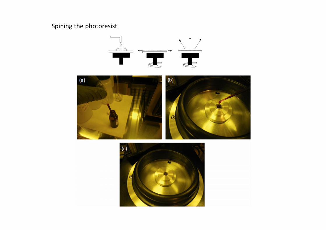
Spining the photoresist

C4S-UTCN
λ=405nm, 40mW/cm2
Clean room utilities Mask aligner

Rack aparaturăTub argon
sursă ioni
Sasintroducere
probă Instalație IBE
Pompaj IBEPompaj sas
Robinet sertardecuplare
The ion beam etching plant (C4S/TUCN)

substratsecvență multistrat
MascăFotorezist pozitiv
Fotoexpunere UVDevelopare
Gravură (etching) Final gravură Indepărtare fotorezist( => microstructuri)
(1) (2) (3)
(4) (5) (6)
Sistem inițial(wafer+secvențămultistrat)
Reprezentare schematică a procesului de transfer de pe mască pewafer corespunzător foto-litografiei cu fotorezist pozitiv

Optical lithography (UTCN)
Suss MicroTech MJB4
Patterning of:
-Micrometric size magnetic objects-Current in plane electric devices
(Hall, GMR, superconducting lines)-Current perpendicular to plane devices
magnetic tunnel junctions,superconducting spin valves
Undercut Neg ma-420
Positive S1813

CIP transport (GMR, AMR, Hall ….)
VH
I
4 points mesurements

Smal
l dim
ensi
onal
ity
syst
ems
Exchange length: scale length of magnetism

10 µm
Example: Modulation of magnetismvia the shape of objects
Smal
l dim
ensi
onal
ity
syst
ems disk wire
In planemagnetization
Longitudinalmagnetization
N S

MezomagnetimMagnetism modulation in reduced dimension objects useful for spintronics
Nanometric-thick thin filmsNi80Fe20 weak stripedomain wall structure
Co stripe domain wall structurePerpendicular to film magnetization
Then Patterned films

Magnetic film / dot with modulatedperpendicular magnetic configuration
Monodomain/vortex in nanometric Co dot
Mezoscopic magnetism at C4S/TUC-N
Object Oriented MicroMagnetic Framework(OOMMF)
Coordinator: Dr. Ing. Coriolan Tiusan: [email protected] France/ TUCN Cluj-Napoca
POS CCE Project 554 2010-2013
http://www.c4s.utcluj.ro/Spintronics.html

SPINTRONIC DEVICES: Current-in-plane transport CIP (GMR, AMR, Hall ….)

Magnetic tunnel junctions/ Data storage and sensors
FeFe
3 ML MgO
-600 -400 -200 0 200 400 600
0
100
200
300
400 4K 300K
TMR
(%)
H(Oe)

Siemens Aktiengesellschaft
Application of spin-valves: GMR angular sensor
GMR angle detector: (spin valve)H.A.M. van den Berg et al JMMM 165, 524, (1997)

MTJS represent the read-head sensor in the high-density hard disk drives
4.0GB from Toshiba's0.85-Inch Hard Disk Drive
From S.S. Parkin, S-H. Yang, Nature Nanotechnology, 10,195–198, (2015)

Magnetic Random Access Memories (MRAM)
The advantages of MRAMs:non volatilelow power consumtion (no mechanicalpieces), compared to hard-diskstable against radiationhigh speed (competitive with SRAM) andlarge density (competitive with DRAM)

Or 3D next generation of memories (RACE-TRACKS)…From S.S. Parkin, S-H. Yang, Nature Nanotechnology, 10,195–198, (2015)
Related Documents