PLEASE SCROLL DOWN FOR ARTICLE This article was downloaded by: [Universita' di Trento] On: 16 May 2011 Access details: Access Details: [subscription number 908206912] Publisher Taylor & Francis Informa Ltd Registered in England and Wales Registered Number: 1072954 Registered office: Mortimer House, 37- 41 Mortimer Street, London W1T 3JH, UK Journal of Modern Optics Publication details, including instructions for authors and subscription information: http://www.informaworld.com/smpp/title~content=t713191304 Nanofabricated atom optics: Atom chips Karolina Brugger a ; Tommaso Calarco bc ; Donatella Cassettari a ; Ron Folman a ; Albrecht Haase a ; Björn Hessmo ad ; Peter Krüger a ; Thomas Maier e ; Jorg Schmiedmayer a a Institut für Experimentalphysik, Universität Innsbruck, Innsbruck, Austria b Institut für Theoretische Physik, Universität Innsbruck, Innsbruck, Austria c ECT*, Villazzano, Italy d Department of Quantum Chemistry, Uppsala University, Uppsala, Sweden e Institut für Festkörperelektronik, Wien, Austria To cite this Article Brugger, Karolina , Calarco, Tommaso , Cassettari, Donatella , Folman, Ron , Haase, Albrecht , Hessmo, Björn , Krüger, Peter , Maier, Thomas and Schmiedmayer, Jorg(2000) 'Nanofabricated atom optics: Atom chips', Journal of Modern Optics, 47: 14, 2789 — 2809 To link to this Article: DOI: 10.1080/09500340008232197 URL: http://dx.doi.org/10.1080/09500340008232197 Full terms and conditions of use: http://www.informaworld.com/terms-and-conditions-of-access.pdf This article may be used for research, teaching and private study purposes. Any substantial or systematic reproduction, re-distribution, re-selling, loan or sub-licensing, systematic supply or distribution in any form to anyone is expressly forbidden. The publisher does not give any warranty express or implied or make any representation that the contents will be complete or accurate or up to date. The accuracy of any instructions, formulae and drug doses should be independently verified with primary sources. The publisher shall not be liable for any loss, actions, claims, proceedings, demand or costs or damages whatsoever or howsoever caused arising directly or indirectly in connection with or arising out of the use of this material.

Welcome message from author
This document is posted to help you gain knowledge. Please leave a comment to let me know what you think about it! Share it to your friends and learn new things together.
Transcript

PLEASE SCROLL DOWN FOR ARTICLE
This article was downloaded by: [Universita' di Trento]On: 16 May 2011Access details: Access Details: [subscription number 908206912]Publisher Taylor & FrancisInforma Ltd Registered in England and Wales Registered Number: 1072954 Registered office: Mortimer House, 37-41 Mortimer Street, London W1T 3JH, UK
Journal of Modern OpticsPublication details, including instructions for authors and subscription information:http://www.informaworld.com/smpp/title~content=t713191304
Nanofabricated atom optics: Atom chipsKarolina Bruggera; Tommaso Calarcobc; Donatella Cassettaria; Ron Folmana; Albrecht Haasea; BjörnHessmoad; Peter Krügera; Thomas Maiere; Jorg Schmiedmayera
a Institut für Experimentalphysik, Universität Innsbruck, Innsbruck, Austria b Institut für TheoretischePhysik, Universität Innsbruck, Innsbruck, Austria c ECT*, Villazzano, Italy d Department of QuantumChemistry, Uppsala University, Uppsala, Sweden e Institut für Festkörperelektronik, Wien, Austria
To cite this Article Brugger, Karolina , Calarco, Tommaso , Cassettari, Donatella , Folman, Ron , Haase, Albrecht ,Hessmo, Björn , Krüger, Peter , Maier, Thomas and Schmiedmayer, Jorg(2000) 'Nanofabricated atom optics: Atom chips',Journal of Modern Optics, 47: 14, 2789 — 2809To link to this Article: DOI: 10.1080/09500340008232197URL: http://dx.doi.org/10.1080/09500340008232197
Full terms and conditions of use: http://www.informaworld.com/terms-and-conditions-of-access.pdf
This article may be used for research, teaching and private study purposes. Any substantial orsystematic reproduction, re-distribution, re-selling, loan or sub-licensing, systematic supply ordistribution in any form to anyone is expressly forbidden.
The publisher does not give any warranty express or implied or make any representation that the contentswill be complete or accurate or up to date. The accuracy of any instructions, formulae and drug dosesshould be independently verified with primary sources. The publisher shall not be liable for any loss,actions, claims, proceedings, demand or costs or damages whatsoever or howsoever caused arising directlyor indirectly in connection with or arising out of the use of this material.

JOURNAL OF MODERN OPTICS, 2000, VOL. 47, NO. 14/15, 2789-2809
Nanofabricated atom optics: atom chips
KAROLINA BRUGGER', TOMMASO CALARCO2v3, DONATELLA CASSETTARI', RON FOLMAN', ALBRECHT HAASE', BJORN HESSM0'i4, PETER KRUGER', THOMAS MAIER' and JORG SCHMIEDMAYER'
Institut fur Experimentalphysik, Universitat Innsbruck, A-6020
Institut fur Theoretische Physik, Universitat Innsbruck, A-6020
ECT*, Villa Tambosiu, Strada delle Tabarelle 286, 1-38050
Department of Quantum Chemistry, Uppsala University, S-75120
Institut fur Festkorperelektronik, Floragasse 7, A-1040 Wien, Austria
Innsbruck, Austria
Innsbruck, Austria
Villazzano, Italy
Uppsala, Sweden
(Received 2 May 2000)
Abstract. Small tight trapping and guiding potentials can be created for neutral atoms moving microns above surfaces patterned with nanofabricated charged and current-carrying structures. Surfaces holding such structures form atom chips which, for coherent matter wave optics, may form the basis for a variety of novel applications and research tools, similar to integrated circuits in electronics. In this paper we describe the basic principles of atom chip experiments.
1. Introduction Microscopic scale atom optics can be realized by bringing cold atoms [ l , 21
close to charged [3-51 and/or current-carrying structures [6-91 which create microscopic potentials for neutral atoms using: (i) the electric interaction between a neutral, polarizable atom and a charged nanostructure, where the potential is Vel = - (ii) the magnetic interaction between the atomic magnetic moment p and a magnetic field B, which is described by the potential Vmaa = -,!is 2. These potentials can also be combined with traditional atom optical elements [lo] such as atom mirrors and evanescent light fields to create a variety of novel atom optical elements at the microscopic scale.
The motivation for miniaturization of atom optics is manyfold: potentials with sizes smaller than the particle de Broglie wave length will allow tight traps with large energy level spacing where only a few levels are populated. The large level spacing reduces the probability of environmental noise inducing unwanted excita- tions. Consequently, coherent transport will be more stable. In addition working within the Lamb-Dicke limit might allow cooling without exciting the atom into higher trap vibrational degrees of freedom.
Journal of Modern Optics ISSN 095C-0340 print/ISSN 1362-3044 online 0 2000 Taylor & Francis Ltd http://www.tandf.co.uk/journals
Downloaded By: [Universita' di Trento] At: 13:00 16 May 2011

2790 K. Brugger et al.
Free-standing structures, such as those described in [8, 11-13], are extremely delicate. If we mount these wires on a surface they become much more robust. In addition, they dissipate heat easier, allowing us to send significantly more current through the wires [6, 71. Using existing nanofabrication technology one can make use of a rich and well-established production procedure, which allows for easy scalability.
A small ground state size together with a precise fabrication technology implies that we know to a very high precision where the atom is and can therefore address it (e.g. with laser light) by high resolution means. Consequently, adjacent atoms can be addressed individually.
In the following paper we present some experiments on magnetic trapping of cold atoms in small, nanofabricated magnetic traps on atom chips [14, 151 reaching the mesoscopic scales required for quantum information processing [ 161, and the various features of the different steps required in such experiments. We first present the basic design principles of microscopic atom optics using current- carrying wires and discuss then a typical design of an atom chip. We then continue by describing the adaptation of standard laser cooling to experiments near surfaces and show how to bring the cold atoms to the surface and to transfer them to the small magnetic traps and guides. Finally, we present some experiments with atoms on the atom chip. Related experiments with surface mounted atom optics, but on a large scale, were performed by groups in Munich [17], JILA [18], and Harvard ~ 9 1 .
2. Design principles The use of magnetic fields for trapping neutral particles first appeared in a 1961
paper by Vladimirskii in the context of neutron physics [20]. A magnetic field minimum acts as a potential mimimum for atoms in a weak field seeking state.' Magnetic field maxima could in principle also trap atoms in high field seeking states, but magnetic field maxima cannot be obtained in free space (Earnshaw's theorem).
In 1933 Frisch and Segre [21] came up with the idea that a current-carrying wire (I,) and a homogeneous bias field (Bb) may produce a well-defined two- dimensional field minimum, in the form of a quadrupole field. This configuration (figure 1) is very easy to miniaturize and mount on a surface, and, more important, it exhibits favourable scaling laws [6-9, 12, 17, 221. The trap depth is given by the bias field, the gradients and curvatures by the magnetic fields from the wire. The distance (ro) between the potential minimum and the wire scales as YO a I,/&, and the gradient (dB/dr) scales as dB/draBb/rO =B; / I , . This means that if the current in the wire is lowered the trap will become tighter and therefore very high gradients are easily obtained with small structures. For example, traps and guides with a gradient of 1OOOGcm-' can be obtained with a current of 0.5A and an external field of 10 G.
Starting from this simple idea one can create various types of guides with external and on chip bias fields using for example one, two, three or four wires (see figure 1 and [7]). 3D-traps can be built by closing such guides by endcaps created
' A weak field seeking state is a hyperfine state for which the energy of the atom increases with increasing magnetic field strength.
Downloaded By: [Universita' di Trento] At: 13:00 16 May 2011
Nanofabricated atom optics: atom chips 2791
0 @ 0
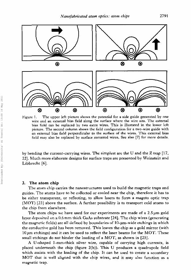
0 0 @ 0 8 Figure 1. The upper left picture shows the potential for a side guide generated by one
wire and an external bias field along the surface where the wire sits. The external bias field can be replaced by two extra wires. This is illustated in the lower left picture. The second column shows the field configuration for a two-wire guide with an external bias field perpendicular to the surface of the wires. This external bias field may also be replaced by surface mounted wires. See also [7] for more details.
by bending the current-carrying wires. The simplest are the U and the 2 trap [17, 221. Much more elaborate designs for surface traps are presented by Weinstein and Libbrecht [6].
3. The atom chip The atom chip carries the nanostructures used to build the magnetic traps and
guides. The atoms have to be collected or cooled near the chip, therefore it has to be either transparent, or reflecting, to allow lasers to form a mageto optic trap (MOT) [23] above the surface. A further possibility is to transport cold atoms to the chip from elsewhere.
The atom chips we have used for our experiments are made of a 2.5 pm gold layer deposited on a 0.6 mm thick GaAs substrate [24]. The chip wires (generating the magnetic fields) are all defined by boundaries of 10-pm-wide etchings in which the conductive gold has been removed. This leaves the chip as a gold mirror (with 10 pm etchings) and it can be used to reflect the laser beams for the MOT. These small etchings do not hinder the loading of a MOT, as shown in [25].
A U-shaped 1-mm-thick silver wire, capable of carrying high currents, is placed underneath the chip (figure 2(b)). This U produces a quadrupole field which assists with the loading of the chip. It can be used to create a secondary MOT that is well aligned with the chip wires, and it may also function as a magnetic trap.
Downloaded By: [Universita' di Trento] At: 13:00 16 May 2011

2792 K. Brugger et al.
Figure 2. (a) The mounted chip before it is introduced into the vacuum chamber. (b) A schematic of the chip design. On top there is a Ga-As-substrate with a gold layer deposited on it. In this gold layer gold is etched away to define the wires used in the experiment. Under the wafer a U-shaped silver wire is put inside a marcor block. All this is mounted on a vacuum feedthrough.
Figure 2 shows the mounted chip before it is introduced into the vacuum chamber used for atom trapping experiments, and a sketch of the components of the atom chip assembly.
In figure 2(c) we present the main elements of a typical chip design. Each of the large U-shaped wires, together with a bias field, creates a quadrupole field. These form a strong magnetic trap. We use this to load atoms into the smaller structures, or as an on-board (i.e. without need for external coils) bias field, for traps created by the thin wire running between them. The thin wires are 1 pm wide and, depending on the contact used, may form a U-shaped or Z-shaped magnetic trap. They may also form a magnetic guide, or a beam splitter for guided atoms.
4. Loading the atom chip To load cold atoms into small magnetic traps on the atom chip we first load a
mirror-MOT [26, 271 with as many atoms as possible. Then we transfer the atoms to a well-aligned M O T generated by a U-shaped wire underneath the chip. We then switch off the light to confine the atoms magnetically within the U-trap. Next we compress the atomic cloud into a fairly large magnetic trap on the chip. After further compression we can transfer the atoms to the micro-trap generated by small wires on the chip.
4.1. Mirror-MOT The first problem to solve is how to obtain a M O T close to a surface. It is clear
that it is difficult to use the conventional six-beam configuration, since a large surface will block at least one of the beams if the trap centre is close to the surface.
This problem has an easy solution using the ideas of Lee et 01. [26], who, in a beautiful experiment, showed that it is possible to build a M O T using a reflecting pyramid and one laser beam, instead of the conventional six-beam configuration (figure 3(a)). The principle behind this M O T is that a circular-polarized light
Downloaded By: [Universita' di Trento] At: 13:00 16 May 2011

Nanofabricated atom optics: atom chips 2793
Figure 3. (a) The pyramid MOT is obtained when one single laser beam is retro- reflected by a four-sided pyramid in the centre of a magnetic quadrupole. The incoming laser beam, with a+-helicity, changes helicity to c- after the first reflection and back to a+ after the second. The beam leaves the mirrors in the same direction as it entered, now counter-propagating the incoming &-light. A quadrupole field (black arrows) with the same symmetry as the pyramid generates the MOT. (b) MOT generated by two trapping beams (I and 11) impinging from opposite directions on a reflecting gold layer deposited on a GaAs-substrate. Trap beam I (11) has helicity a+ (a-) before reflection off the chip and a- (a+) after reflection. This light configuration generates a MOT together with the magnetic field illustrated with the arrows. The magnetic field is obtained either by a set of external quadrupole coils, or by superimposing the field from a current-carrying U-shaped wire underneath the chip with a homogeneous bias field. In both cases, the position of the atomic cloud is determined by the centre of the quadrupole field.
beam changes helicity upon reflection from the surface. This feature generates the polarization configuration needed for a MOT.
Using this idea, it is possible to generate a MOT with only one mirror at the price of introducing more laser beams. Figure 3(b) illustrates how a mirror-MOT can be obtained. T h e six laser beams needed for the MOT are formed from four beams by reflecting two of them off the chip surface [14, 171. Four circularly polarized light beams enter the chamber; two counter-propagate parallel to the surface of the chip, while the other two, impinging on the surface of the chip at a 45 degree angle, are reflected by the gold layer. Hence, atoms above the chip encounter six light beams in the correct configuration of polarization needed for the formation of a M O T . T o ensure the correct magnetic field configuration for the M O T , one of the reflected light beams has to be in the axis of the MOT coils. A schematics of the experimental setup is shown in figure 4.
In the first step of our experiments we load lo8 7Li atoms for 20s from an effusive atomic beam into such a mirror-MOT (figure 4) using a red laser detuning of 25 MHz and a total laser power of about 150mW. An electro-optic modulator produces sidebands of 812MHz (30%) one of which is used as a repumper. To increase the loading rate we use an additional slow beam (20mW, l 0 0 M H z red detuned) directed through the M O T into the oven. T h e atomic cloud is typically 1 m m in diameter (FWHM).
In the experiment, we use the gold layer of the chip as a mirror. T h e shadows (diffraction patterns) from the 10pm etchings do not disturb the MOT signifi- cantly [25, 281. T h e loading of such a mirror-MOT seems to be as efficient as a
Downloaded By: [Universita' di Trento] At: 13:00 16 May 2011

2794 K. Brugger et al.
Figure 4. Experimental setup: four circularly polarized light beams enter the chamber; two counter-propagate parallel to the surface of the chip, while the other two, impinging on the surface of the chip at 45 degrees, are reflected by the gold layer. Hence, atoms above the chip encounter six light beams in the correct configuration of polarization needed for the formation of a MOT. The chip, the underlying U- trap, and the bias field, are oriented in such a manner as to provide a quadrupole field with the same orientations as the MOT coils. The oven, the effusive beam, and the three cameras observing the atomic cloud are also shown.
regular MOT. Figure 5 shows a top view of the mirror-MOT sitting above the chip with some of its electric connections.
The large external quadrupole coils are then switched off while the current in the U-shaped wire underneath the chip is switched on (up to 16 A), together with an external bias field (8G). This forms a nearly identical, but spatially smaller, quadrupole field as compared to the fields of the large coils (figure 6). The atoms are thus transferred to a secondary M O T which by construction is always well aligned with the chip.* By changing the bias field, the M O T can be shifted close to the chip surface (typically, 2mm). The laser power and detuning are changed to further cool the atoms, giving us a sample with a temperature below 200pK.
Having trapped the atoms in the U-MOT we have solved the problem of how to bring cold atoms to a well-defined position close to a surface. We now wish to
*We actually run some of our experiments using only the U-shaped wire, skipping the external quadrupoles completely. The loading of the MOT is decreased significantly, due to the smaller collecting volume of the U-MOT. We believe however that this configuration may be optimized further. See also [17].
Downloaded By: [Universita' di Trento] At: 13:00 16 May 2011

Nanofabricated atom optics: atom chips 2795
-
Figure 5. Pictures showing the loading of cold atoms close to the surface of an atom chip: column (i) shows the view from the top (camera l), column (ii) the front view (camera 2), column (iii) the side view (camera 3) and (iv) a schematic of the wire configuration. Current-carrying wires are highlighted in black. The front and side view shows two images: the upper is the actual atom cloud and the lower is the reflection on the gold surface of the chip. The distance between both images is an indication of the distance of the atoms from the chip surface. The top row shows a picture from the mirror-MOT, taken from above. The side views are omitted, because the MOT is outside the field of view of camera 2 and 3. The second row shows atoms trapped in the U-MOT created by current in the large U shaped wire underneath the chip and a homogeneous bias field. The bottom row displays atoms in a magnetic trap generated by the U-wire field. The pictures of the magnetically trapped atomic cloud are obtained by fluorescence imaging using a short laser pulse (typically 0.5 ms).
transfer the atoms to magnetic traps on the chip. For this the quadrupole field of the wire underneath the chip is useful since it may also function as a magnetic trap.
4.2. U-magnetic trap In the next step, the laser beams are switched off and the quadrupole field
serves as a magnetic trap in which the weak-field-seeking atoms are attracted to the minimum of the field. Typically we can, without optical pumping, trap up to 20% of the atoms in the MOT in the U-magnetic trap (figure 5).
Atoms in the magnetic traps are then observed by fluorescence imaging. For this we switch on molasses laser beams for a short time (typically less than 0.5 ms), and the scattered light is imaged by three CCD cameras as shown in figure 4. We
Downloaded By: [Universita' di Trento] At: 13:00 16 May 2011

2796 K . Brugger et al.
Figure 6. The magnetic field of the U-shaped wire and an external bias field. This field may function both as a magnetic trap, or as the quadrupole field needed for a MOT.
use a sufficiently short exposure time to avoid blurring of the image due to atomic motion. One has also to select the camera positions wisely to avoid ghost images caused by diffraction off the etchings in the atom chip surface.
Without the difficulties of near surface shadows hindering the MOT, the magnetic trap can now be lowered further towards the surface of the chip. This is simply done by increasing the bias field (up to 19G).3 Atoms are now close enough that they can be trapped by the chip fields. The loading of the chip has begun.
4.3. Loading smaller traps The second problem (the first being the mirror-MOT) is how to transfer atoms
from the large U-trap to a very small trap or guide on the chip, i.e. how to compress a large magnetic trap in such a way that it can release the atoms in a smaller trap without large losses. The basic principle is to first switch on the current through the small trap, and then ramp down the current in the wire creating the large trap. This whole process can be accompanied by an appropriate change in the bias field to further compress the atoms in the trap. The atoms following the magnetic field minimum make a transition from a large trap to a smaller one very smoothly and virtually without loss.
In figure 7 we show examples of how such loading of a small trap occur. In the case when the centre of the large trap is well aligned with the small trap, loading is optimal. Also, in the case of a mismatch, transfer may still be efficient. A limiting factor is the strength of the acceleration forces the atoms experience during transfer.
4.4. Transfer to the atom chip In the next step of the loading of an atom chip we transfer the atoms from the
large U-trap to a trap on the chip [14]. In our case, for example, a current of 2 A is passed through each of the two 200 pm U-shaped wires on the chip and the current in the U-shaped wire located underneath the chip is ramped down to zero.
We may compress the magnetic trap either by increasing the bias field or by lowering the current in the wire. If the bias field is increased, the depth of the trap also increases.
Downloaded By: [Universita' di Trento] At: 13:00 16 May 2011

Nanofabricated atom optics: atom chips 2797
(a) B = 10 G I = 2x2 At300 mA
(a) B = 10 G I = 2 N300 mA
Matched loading: (b)B= 10G (c) B = 10 G (d )B=50G
I = 2 ~ 0 . 5 N300 mA I = 2x0 m m A I = 2x0 At300 mA
Unmatched loading: (b)B = 10G (c)B= 10G (d )B=lOG
I = 0.5 N300 mA I = O N 3 0 0 mA
Figure 7. Position of the surface-mounted wires and equipotential lines for the trapping potential: top row shows the transfer from two large 200 pm wire to one small 10 pm wire. In (a)-(c) the current in the small wire is constant at 300mA and the bias field constant at 10 G. The current in the two large wires is decreased from 2 A in each wire to zero. This transfers the atoms to the small wire. (d) By increasing the bias field the trap can be compressed further. The lower row shows the transfer from one large 200p wire to one small 10pm wire. In (a)-(d) the current in the large wire drops from 2 A to zero. The thick line shows how the trap centre moves during transfer.
This procedure brings the atoms closer to the chip, typically a few hundred micrometres, and transfers the atoms to a magnetic trap formed by the two U- shaped wires on the chip. The magnetic trap on the chip can then be compressed further by increasing the bias field, as shown in figure 8.
4.5. Surface traps Finally, the 10 pm wire trap is loaded from the 200 pm wire trap in the same
way as the 200pm wire trap was loaded from the U-trap. The lOpm wire first receives a current of typically 300mA. Then the current in both the U-shaped wires is ramped down to zero (figure 7). Atoms are now typically a few tens of microns above the surface (figure 8) trapped in a microfabricated magnetic trap.
During the transfer from the large magnetic trap to the small lOpm trap the density of the atomic cloud is increased by a factor up to 350. As the trap is compressed, the temperature of the atoms rises, and if the trapping potential is not deep enough, atoms are lost. In our case, the trap depth is uniquely determined by the bias field used, which leads to depths rnFgFpBIB1 ranging between -6MHz (-0.25 mK) for the 8 G bias field and = 1 to -70MHz (-3 mK) for the 50 G
Downloaded By: [Universita' di Trento] At: 13:00 16 May 2011

2798 K . Brugger et al.
camera 1 top view
camera 2 front viem
camera 3 side view
Figure 8. Compressing cold atoms on an atom chip: the top rows shows the view from the top (camera I), the second row the front view (camera 2), and the third row the side view (camera 3). The front and side views show two images: the upper is the actual atom cloud and the lower is the reflection of the gold surface of the chip. The distance between both images is an indication of the distance of the atoms from the chip surface. The first three columns show atoms trapped on the chip with the two U-shaped wires. The compression of the trap is accomplished by increasing the bias field. The last row displays images from a 2-trap created by 300mA current through the 10pm wire in the centre of the chip. The pictures of the magnetically trapped atomic cloud are obtained by fluorescence imaging using a short laser pulse (typically 0.5 ms).
bias field and ImF( = 2. This adiabatic heating and the finite trap depth limited the transfer efficiency for atoms from the large magnetic trap into the smallest chip trap to <SO%. The main loss of atoms occurs in the transfer from the U-MOT to the U-magnetic trap, and not in the transfer to smaller traps.
5. Experiments on the atom chip Once the atoms are trapped on the chip, we can study the magnetic traps and
atom optical elements which can be built with such micro-traps.
5 .1 . Traps The small wires used are either U-shaped, 2-shaped, or H-shaped. The main
difference between these is how the field from the ‘endcaps’ contributes to the total magnetic field. The U-trap is, as mentioned above, a quadrupole trap, the 2-trap is an Ioffe-Pritchard type, and the H-trap can be either of these. Also, there are minor differences in the alignment of the traps with respect to the larger double U -trap.
Downloaded By: [Universita' di Trento] At: 13:00 16 May 2011

Nanofabricated atom optics: atom chips 2799
In one set of experiments [14] we investigated how much the traps and guides can be compressed. This is done by ramping up the bias magnetic field. In this process we typically achieve gradients of >25 kGcm-’. By applying a bias field of 40 G and a current of 200 mA in the 10 pm wire we achieve trap parameters with a transverse ground state size below 100nm and frequencies of above l00kHz. Thereby we achieve the trapping parameters required by quantum computation proposals [16]. We remind the reader that as the de-Broglie wavelength is of the order of 0.1-1 pm for temperatures of the order 1004.1 pK respectively, the ground state sizes achieved are adequate for the purpose of coherent transport- ation, as long as the initial temperature can be maintained on the atom chip.
In these small traps, the atom gas can be compressed to the point where direct visual observation is difficult. In such cases, we observe atoms after guiding or trapping, by ‘pulling’ them up from the surface into a less compressed wire trap (by increasing the wire current or decreasing the bias field).
In a different experiment we used thick wires on the chip to create an on-chip bias field for the trapping with the thin wire. This is done by sending current through the two U-shaped wires, in the opposite direction with respect to the current in the 10 pm wire. These create a magnetic field parallel to the chip surface, substituting the external bias field. Hence, we demonstrate trapping of atoms on a self-contained chip.
Another interesting question concerns the high atom density in the compressed trap, and the collision rate obtainable. Since we use a trapped atomic sample consisting of three different spin states IF = 2, ?nF = 2), IF = 2, mF = I ) , and IF = 1, mF = - 1) the large compression also increases the rate of inelastic two- body spin exchange collisions dramatically. This rate is, for our Li sample, similar to the elastic collision rate [29] and is therefore a good estimate of the achievable collision rates in a polarized sample. From measured decay curves we estimate the collision rate to be in the order of 20 s-l for atoms in a typical small chip trap. This estimate of scattering rate in small chip traps is supported by the observation that the atoms expand rapidly into the wire guide, indicating that energy gained from the transverse compression of the trap is transformed efficiently into longitudinal velocity at a high rate.
5.2. Guides T o achieve mesoscopic atom optics on the atom chips, it is essential to have
reliable transport of atoms on the chip. The most obvious device for this is an atomic guide using a single wire with a bias field, where the atoms move along the guide due to their thermal velocity.
The atoms may be sent into such a guide in several different ways. The most direct method is to load the guide directly from a larger trap and simply skip the small surface trap.
Second, it is possible to leak atoms from a microtrap into a magnetic guide (figure 9). This is achieved by controlling the barrier height between the trap and the guide, where the barrier is simply the ‘endcap’ discussed earlier, which may be controlled by changing the current in the trap.
Third, one may simply open up the trap by sending current in wires other than those defining the trap. For instance, the 2-trap may be transformed into an L- shaped guide simply by switching the direction of one of the outgoing leads. In our experiment this is done by running the current through a different 10 pm section of
Downloaded By: [Universita' di Trento] At: 13:00 16 May 2011

2800 K. Brugger et al.
Figure 9. Loading an atom guide by leaking atoms from a reservoir created by a U-trap into the guide by ramping down the current in the U.
the thin wire. We can in this way observe atoms expanding along the guide (see figure 10).
5 . 3 . Beam splitter We may combine the wire guides described in the previous section to build
more complicated atom optical elements. The simplest of these elements is a beam splitter.
Using two guides it is possible to design potentials where at some point two different paths are available for the atom. This can be realized using different configurations, among which the simplest and most advantageous is a Y-shaped wire [15]. Such a beam splitter has one accessible input for the atoms, that is the central wire of the Y, leading back to the initial magnetic trap, and two accessible outputs corresponding to the right and left wires. Depending on how the current I in the input wire is sent through the Y, atoms can be directed to the output arms of the Y with any desired ratio (figure ll(b)).
We investigate the Y-wire beam splitter by opening up a small surface trap, thus expanding the atomic cloud along the guide leading to the beam splitter. Figure l l (b) shows images taken after 16ms of guiding in the beam splitter. The first two pictures are obtained at &ias = 12 G by passing a current of 0.8 A only through one of the output wires; atoms can therefore turn either left or right. In the third and fourth pictures the atoms experience a splitting potential, the current being sent equally through both outgoing arms of the Y-shaped wire. The images are taken with bias fields of 12 G and 8 G respectively. At 12 G the atoms are clearly more compressed.
By changing the current ratio between the two outputs, and simultaneously keeping the total current constant, we may control the probability of going left and right. Typical data for a beam splitter experiment using 8 G bias field are shown in figure 12. Here, the number of atoms in each arm is determined by summing over
Downloaded By: [Universita' di Trento] At: 13:00 16 May 2011

Nanofabricated atom optics: atom chips 2801
Figure 10. Cold atoms in microtraps and guides on an atom chip: top row shows atoms in a microscopic trap 20pm above the chip surface. Bottom row displays atoms propagating in a guide. Current-carrying wires are highlighted in black.
Figure 11. Beam splitter on a chip: (a) chip schematic and (b) fluorescence images of guided atoms. As explained in the text, the two large U-shaped 200pm wires are used to load atoms onto the lOpm Y-shaped wire. In the first two pictures in (b), current is drawn only through one side of the Y, therefore guiding atoms either to the left or to the right; in the next two pictures, taken at two different guide gradients, the current is divided in equal parts and the guided atoms split into both sides.
Downloaded By: [Universita' di Trento] At: 13:00 16 May 2011

2802
1
K. Brugger et al.
0 0.2 0.3 0.4 ' 0.5 0.6 0.7 0.8 0.9
current ratio Figure 12. Switching atoms between left and right by changing the current ratio in the
two outputs and keeping the total current constant at 0.8A. The points are measured values while the lines are obtained from Monte Carlo simulations with a 3 G field along the input guide. The kinks in the lines are due to MC statistics.
the density distribution. When the current is not balanced, the side carrying more current is preferred due to better mode matching with the incoming guide. It can be noted that the 50/50 atomic splitting ratio occurs for a current ratio different from 5 O : S O . This is due to additional fields along the input guide which introduces a difference in the output guides which can be compensated by using different currents. The solid lines shown in figure 12 are obtained with Monte Carlo simulations of an atomic sample at T = 250 pK propagating in the Y beam splitter.
6. Vision and outlook We would like to conclude with a long-term outlook: atom optics has proven to
be an extremely successful tool for research into the foundations of quantum theory concerning topics such as matter-wave interference, entanglement and the uncertainty principle, and for the development of technological applications such as clocks and acceleration sensors. Most of the present experiments are put together as a macroscopic apparatus from single atom optical elements, in a way similar to the first electronic devices which were built from parts performing single tasks.
Integrating many elements to control atoms onto a single device, an atom chip, will make atom physics experiments much more robust and simple. Neutral atom manipulation using integrated microdevices will combine the best of two worlds: the ability to use cold atoms - a well-controllable quantum system (for example as a qubit), and the immense technological capabilities of nanofabrication and microelectronics to build highly complex experiments for manipulating the atoms. This may allow much more complicated tasks in atom manipulation to
Downloaded By: [Universita' di Trento] At: 13:00 16 May 2011

Nanofabricated atom optics: atom chips 2803
be performed in a way similar to that in which integration of electronic elements allowed the development of new powerful electronic devices.
On the atom optical side this will include further miniaturization of traps and guides for neutral atoms by various combinations of magnetized, current-carrying and charged microstructures building a toolbox for atom manipulation micro- metres above a surface, in structures similar to the quantum wells, quantum wires and quantum dots of mesoscopic quantum electronics. These atom chip com- ponents will include a reliable source of cold atoms with an efficient loading mechanism. Our experiments have demonstrated traps with parameters similar to BEC traps which should allow on-chip creation of a degenerate quantum gas as a reservoir of cold atoms for the experiments. From these, atoms will be transported in a controlled and coherent way to the designed experiments, preferably in single- mode guides or movable potentials. Ideally one wants routine single-atom state selective loading, preparation and manipulation. For instance, by adiabatically turning on a periodic potential within a condensate, it is possible to achieve a phase transition from the superfluid BEC to a Mott insulator phase with regular filling of the sites of the periodic potential, as already proposed for the case of optical lattices [30]. All this can be made state dependent.
Another important component will be the integration of light optics on the atom chip: for example light guides and micro-optics can be fabricated on the atom chip to bring laser light to the atoms for manipulation of internal and external degrees of freedom. This can be done using evanescent waves, or direct focusing of light with high numerical aperture micro-optics onto the atoms trapped in the microtraps. Here the precision of nanofabrication (typical <lo0 nm) allows for the addressability of specific atoms, as ground state sizes will be extremely small and precisely aligned.
A third component of the integrated chip will be the detection of internal degrees of freedom as well as the mere existence of the atom at a specific location. Here one can learn from single-molecule spectrosopy using nano-optics and cavity QED. As an example one can imagine having a light wave guide interferometer on the chip which will measure the phase shift introduced by the atoms in the microtrap, similar to environmental sensors. One can also imagine fabricating a microscopic cavity coupled to two waveguides. An atom in the cavity will influence the transmission and lead to a detectable signal. A different approach to detecting the atoms can be a scanning probe technique, the probe being a microsphere cavity with one of its whispering gallery modes tuned close to the resonance frequency of the atoms. An atom in the evanescent wave of the microsphere cavity will influence the transmission/coupling probability of light into the microsphere and lead to a detectable signal.
All of these and probably even the light sources, control electronics, etc., could be on-board a self-contained atom chip which can then be used for matter wave experiments and devices.
6.1. Mesoscopic physics The atom optical potentials for neutral atoms moving microns above surfaces,
using nanofabricated charged and current carrying structures, described in this work, are very similar in scale to the electric potentials confining electrons in mesoscopic quantum electronics [31, 321. In both cases, one deals with potentials,
Downloaded By: [Universita' di Trento] At: 13:00 16 May 2011

2804 K. Brugger et al.
where at least one dimension is comparable to the de-Broglie wavelength of the trapped/guided particle.
One can therefore easily imagine the creation of low-dimensional and meso- scopic devices for atoms moving microns above surfaces. Surfaces carrying such structures form atom chips which, for coherent matter wave optics, may form the basis for a variety of novel applications and research tools, similar to integrated circuits for electronics.
Examples of interesting physics applications are manifold and range from studies of coherence and decoherence in mesoscopic systems to experiments investigating quantum gases in low-dimensional potentials [33].
6.2. Quantum information Quantum optical techniques allow accurate control of the coherent evolution of
quantum systems, and are therefore promising candidates for the implementation of quantum logic [34]. Quantum computing requires (i) storage of the quantum information in a set of two-level systems (qubits), (ii) the processing of this information using quantum gates, and (iii) reading out the results. So far only a few systems have been proposed for the realization of quantum computer models. Examples include trapped ions, cavity QED, and neutral trapped atoms, NMR and solid state systems using nuclear spins, quantum dots and Josephson junc- tions. Novel schemes can be envisioned by using the atom optical approach outlined in this paper, which combines the outstanding features of quantum optical proposals (in particular quantum control and long decoherence times) with the technological capabilities of engineering microstructures implying scal- ability, a feature usually associated with the solid state proposals and required by actual computations, including error correction procedures, to keep decoherence under control. In all such schemes, each particle carries a qubit in two internal, long-lived states lo), 11) (e.g. two different hyperfine structure states). The most delicate feature to implement is a fundamental two-qubit quantum gate, i.e. a phase gate with the truth table
To realize this transformation, one can consider state selective changes of the trapping potential, such that the atoms pick up a phase due to interaction only if they are in state 11) [35, 161. A physical implementation of this scenario requires an external field which produces time-dependent conservative trap potentials. T o obtain conditional dynamics, either the trapping forces should be state-dependent, or the interaction term, or both. Since neutral atoms interact via collisions, described by a contact potential, in order for the atoms to interact, their wavefunctions have to overlap with each other at some point. Different regimes are possible for the time dependence of the potential, leading to specific schemes for entanglement manipulation, suitable for different physical implementations. In particular, the limits of slow (adiabatic) and fast (sudden) potential changes are both interesting and have been analysed elsewhere [35, 161.
Downloaded By: [Universita' di Trento] At: 13:00 16 May 2011

Nanofabricated atom optics: atom chips 2805
Figure 13. Moving potentials for quantum information processing: configurations at time 0, T (a) and at t (b). The solid (broken) curves show the potentials for particles in the internal state 10) (11)). Central positions f i ( t ) and displacements 6xPr(t) as defined in the text.
One way of controlling the interaction between the particles is to move the central position of the potentials towards each other in a state-dependent way while leaving the shape of the potential unchanged. Let us assume that we can design the trapping potentials such that the atom i = 1,2 in the internal state [pi) experiences a potential Vf'(x, t ) = V(xi + bxp8( t ) ) which is initially ( t = 0) centred at position x i . We assume that we can move the centra of the potentials according to the trajectories 6 x p i ( t ) , chosen in such a way that ~ X ' ~ ( O ) = b x p i ( ~ ) = 0 (figure 13), and that the first atom collides with the second one only if they are in state 10) and [ I ) , respectively.
The fact that xi does not depend on the internal atomic state and that the shape of the two potentials is the same at times t = 0, T allows one to easily change the internal state at those times by applying laser pulses.
The interaction between the particles can be controlled also in another way, for example by changing with time the shape of the potentials depending on the particles' internal states. We will consider raising and lowering a potential barrier between the two atoms as shown in figure 14.
According to figure 14(a), the potential is initially composed of two separated wells. Ideally, the atoms have been cooled to the vibrational ground states of the two wells. At t = 0, the barrier between the wells is suddenly removed in a selective way for atoms in internal state 10): an atom in state 11) feels no change (solid line in figure 14 (b)), whereas one in state 10) finds itself in a new harmonic potential, centred on x = 0 with lower frequency (broken line in figure 14(b)). The atoms are allowed to oscillate for some time, and then at t = T (where T is a mulitple of To,,, the oscillation period in the well of figure 14(b) (dashed line)), the barrier is suddenly raised again to trap them at the original positions. During this process the atoms acquire a kinematic phase due to their oscillations within the wells, and also, if they collide, an interaction phase due to the collision, which can then be adjusted to the desired value of f x to obtain the transformation (1).
State-dependent potentials of this kind can be implemented by means of static electric and magnetic trapping forces on nanofabricated atom chips. The interplay
Downloaded By: [Universita' di Trento] At: 13:00 16 May 2011

2806 K . Brugger et al.
Figure 14. Switching potentials for quantum information processing: configuration at times t < 0, t > T (a) and at 0 5 t 5 7 (b). The solid (broken) curves show the potentials for particles in the internal state 11) (10)).
between the state-dependent magnetic term Vmag oc rn~lBl (with IF, r n ~ ) being the internal state of an atom in a magnetic field B) and the state-independent electric one I/kl 0: ]El2 can be exploited in order to obtain a trapping potential whose shape depends on the internal state of the atoms [16]. As an example, we consider a chip surface with periodic magnetization (analogous to a magnetic atomic mirror [S]), immersed in an external bias field, generating a field whose modulus has minima along x and z, where atoms can be trapped. Microscopic electrodes can be nanofabricated on the mirror’s surface [4] below each pair. Charging them produces an attractive potential for atoms, giving confinement along the y direc- tion. The barrier between the two nearest wells can be lowered by increasing the charge on the corresponding electrode. If the logical states are chosen in such a way that 11) has an interaction with the magnetic field twice as high as lo), then the charge can be adjusted so that the barrier is removed just for atoms in internal state lo), but remains still in place for atoms in 11). In this way it is possible to design a potential with the characteristics described in figure 14. On the other hand, rotating the magnetic bias field induces a displacement in the minima of the magnetic field, which tends to displace the atoms trapped there. A suitable periodic electrostatic field would be able to compensate for this effect by keeping atoms in state 10) at their position, while at the same time allowing for those in state 11) to move. This would then constitute an implementation of the scenario of figure 13.
6.3. Open problems A limiting factor for atom chip design and experiments will be the coherence
and decoherence properties of neutral atoms in these microtraps and guides. The specific influence of the nearby hot surfaces [36] containing the trapping structures will be very important. This will limit how close one can get to the surface, and thereby how small the traps and guides may be made, and consequently, what
Downloaded By: [Universita' di Trento] At: 13:00 16 May 2011

Nanofabricated atom optics: atom chips 2807
potential steepness may be reached. At some point the van der Waals interaction between the atom and the surface will become dominant. The technique with well- aligned microtraps close to surfaces can be used to study this elusive force in a new way.
It will be interesting to identify the mechanisms through which decoherence limits quantum computing in atom optical microstructures, as well as strategies to fight decoherence itself.
In the microtraps it is possible to compress the atomic cloud to extreme densities, where molecular properties and three-body collisions become important. Ground state sizes of the same order as the scattering length can be achieved. In this regime, scattering itself will be modified by the external potential. Similarly, it might be possible to control atomic collisions and chemical reactions, by trans- porting atoms to a collision centre where they can be put at a well chosen distance from each other.
7. Conclusion In this work we have successfully realized the first steps of many still needed in
this direction. A final integrated atom chip should have a reliable source of cold atoms with an efficient loading mechanism, single-mode guides for coherent transportation of atoms, nanoscale traps, movable potentials allowing controlled collisions for the creation of entanglement between atoms, extremely high resolu- tion light fields for the manipulation of individual atoms, and internal state- sensitive detection such as cavity QED to read out the result of the processes that have occurred (for example: the quantum computation). All of these, including the bias fields and probably even the light sources, could be on-board a self-contained chip. This would involve sophisticated 3D nanofabrication and the integration of a diversity of electronic and optical elements, as well as extensive research into fundamental issues such as decoherence near a surface. Such a robust and easy to use device would make possible advances in many different fields of quantum optics: from applications such as clocks and sensors to implementations of quantum information processing and communication.
Acknowledgments We would like to thank A. Mitterer for help in the experiments. Atom chips
used in the preparation of this work and in the actual experiments were fabricated at the Institut fur Festkorperelektronik, Technische Universitat Wien, Austria, and the Sub-micron center, Weizmann Inst. of Science, Israel. We thank E. Gornik, C. Unterrainer and I. Bar-Joseph of these institutions for their assistance. We also thank R. Cote for his theoretical insights regarding atom collisions. Last but not least, we gratefully acknowledge P. Zoller who is responsible for the theoretical vision. This work was supported by the Austrian Science Foundation (FWF), project SFB F15-07, and by the European Union, contract Nr. IST-1999- 11055 (ACQUIRE), TMRX-CT96-0002, HPMF-CT-1999-00211 and HPMF- CT-1999-00235. B.H. acknowledges financial support from Svenska Institutet, and T.C. financial support from Instituto Trentino di Cultura (ITC).
Downloaded By: [Universita' di Trento] At: 13:00 16 May 2011

2808 K. Brugger et al.
References [ l ] A good overview of laser cooling is given in: E. Arimondo, W. D. Phillips, F. Strumia
(eds), 1992, Laser Manipulation of Atoms and Ions (North Holland); CHU, S., 1998, Rev. Mod. Phys., 70, 685; COHEN-TANNOUDJI, C., 1998, Rev. Mod. Phys., 70, 707; PHILLIPS, W. D., 1998, Rev. Mod. Phys., 70, 721.
[2] ANDERSON, M. H. et al., Science, 269, 198; DAVIS, K. B. et al., Phys. Rev. Lett., 75, 3969; BRADLEY, C. C., SACKET, C. A., and HULET, R. G., 1995, Phys. Rev. Lett., 75, 1678. For a complete list of references see also the BEC Homepage http:// amo.phy .gasou.edu/bec. html
[3] SCHMIEDMAYER, J., 1996, Habilitationsschrift, Universitat Innsbruck; DENSCHLAG, J., and SCHMIEDMAYER J., 1997, in Proceedings of the International Quantum Coherence Conference, Boston (Singapore: World Scientific).
[4] SCHMIEDMAYER, J., 1998, Eur. Phs. J . D, 4, 57-62. [5] HINDS, E. A., and HUGHES, I. G., 1999, J. Phys. D, 32, R119-R146. [6] WEINSTEIN, J. D., and LIBBRECHT, K., 1995, Phys. Rev. A, 52, 4004. [7] DRNDIC, M. et al., 1998, Appl. Phys. Lett.., 72, 2906; THYWISSEN, J. H., et al., 1999,
[8] DENSCHLAG, J., et al., 1999, Appl. Phys. B, 69, 291-301. [9] CASSETTARUI, D., et al., 2000, Appl. Phys. B, 70, 721 DO1 10.1007/s003400000297.
[lo] For an overview see ADAMS, C. S., SIGEL, M., and MLYNEK, J., 1994, Phys. Rep, 240, 143; BERMAN, P., 1997, Atom Interferometry (New York: Academic Press), and references therein.
[ 113 SCHMIEDMAYER, J., 1992, in X V I I I International Conference on Quantum Electronics: Technical Digest, edited b y G. Magerl (Vienna: Technische Universitat Wien), Vol. 9, p. 284; 1995, Appl. Phys. B, 60, 169; 1995, Phys. Rev. A, 52, R13.
[12] DENSCHLAG, J., UMSHAUS, G., and SCHMEIDMAYER, J., 1998, Phys. Rev. Lett., 81, 737. [13] FORTAGH, J. et al., 1998, Phys. Rev. Lett., 81, 5310; FORTAGH, J., OTT, H., GROSSMANN,
A., and ZIMMERMANN, C., 2000, Appl. Phys. B, 70, 701-708 DO1 10.1007/ s003400000251.
[14] FOLMAN, R., et al., 2000, quant.ph/9912106, Phys. Rev. Lett., 84,4749. For experiment with large structures (>100pm) see also [17-191.
[15] CASSETTARI, D., et al., 2000, quant-ph/0003135, to appear in Phys. Rev. Lett. [16] CALARCIO, T., et al., 2000, Phys. Rev. A, 61, 022304; BRIEGEL, H.-J., et al., 2000,
[17] REICHEL, J., HANSEL, W., and HANSCH, T. W., 1999, Phys. Rev. Lett., 83, 3398. [18] MULLER, D., et al., 1999, Phys. Rev. Lett., 83, 5194. [19] DEKKER, N. H. et al., 2000, Phys. Rev. Lett., 84, 1124. [20] VLADIMIRSKII, V. V., 1961, Sov. Phys. JETP, 12, 740. [21] FRISCH, R., and SEGRE, E., 1933, Z. f . Physik, 75, 610. [22] HAASE, A., CASSETTARI, D., HESSMO, B., and SCHMIEDMAYER, J. Submitted to Phys. Rev.
[23] RAAB, E. L. et al., 1987, Phys. Rev. Lett., 59, 2631. [24] The chip is produced using standard nano-fabrication. A detailed account will be given
[25] DENSCHLAG, J., CASSETTARI, D., and SCHMIEDMAYER, J., 1999, Phys. Rev. Lett., 82,
[26] LEE, K. I., KIM, J. A., NOH, H. R., and JHE, W., Opt. Lett., 21, 1177. [27] SCHNEBLE, D., GAUCK, H., HARTL, M., PFAU, T., and MLYNEK, J., in Proceedings of
the International School of Physics “Enrico Fermi” on “Bose-Einstein Condensation in Atomic Gases”, Varenna, 7-17 July 1998, edited by M. Inguscio, S. Stringari, C. Wieman, p. 469.
Eur. Phys. J . D, 7, 361.
J . Mod. Opt., 46, 415.
A. For surface mounted U and Z traps see also [17].
in T. Maier et al., to be published.
2014.
[28] DENSCHLAG, J., 1998, PhD thesis. Universitat Innsbruck. [29] COTE, R., private communication. A description of the s-wave estimate approximation
can be found in COTE, R., DALGARNO, A., WANG, H., and STWALLEY, W. C., Phys. Rev A , 57 R4118; COTE, R., TIMMERMANA, E.TOMMASSINI, P., 1998, in New Directions in Atomic Physics, edited by Whelan et al. (New York: Kluwer Academic/ Plenum Publishers), p. 71; TIMMERMANS, E. and COTE, R., 1998, Phys. Rev. Lett., 80, 3419.
Downloaded By: [Universita' di Trento] At: 13:00 16 May 2011
Nanofabricated atom optics: atom chips 2809
[30] JAKSCH, D. et al., 1998, Phys. Rev. Lett., 81, 3108-3111. [31] IMRY, Y., 1987, Introduction to Mesoscopic Physics (Oxford: Oxford University Press). [32] BUKS, E. et al., 1998, Nature, 391, 871-874. [33] OLSHANII, M., 1998, Phys. Rev. Lett., 81, 938. [34] For a review of quantum computing in general see for example: 1998, Phys. World, 11
(3), 33, special issue on quantum information; PLENIO, M. B., and VEDRAL, V., 1998, Contemp. Phys., 39, 431; VEDRAL, V., and PLENIO, M. B., 1998, Prog. Quant. Electron., 22, 1; STEANE, A. M., 1998, Rep. Prog. Phys., 61, 117; BOUWMEESTER, D., EKERT, A,, and ZEILINGER, A. (eds), 2000, The Physics of Quantum Information (Springer-Verlag); BENNET, CH., and DIVINCENZO, D., 2000, Nature, 404, 247.
[35] JAKSCH, D. et a1.,1999, Phys. Rev. Lett., 82, 1975-1978. [36] HENKEL, C., and WILKENS, M., 1999, Europhys. Lett., 47, 414; HENKEL, C., POTTING,
S., and WILKINS, M., 1999, Appl. Phys. B, DO1 10.1007/~993409900189.
Downloaded By: [Universita' di Trento] At: 13:00 16 May 2011
Related Documents