NANOELECTRONICS :: TURBO STORAGE FOR THE COMPUTERS OF TOMORROW :: GETTING STARTED WITH SPINTRONICS :: INSPIRED BY BIOLOGY The Magazine from Forschungszentrum Jülich 01|2010 RESEARCH in Jülich

Nanoelectronics - Research in Jülich (1/2010)
Mar 19, 2016
Information and communications technologies are the driving force behind growth and innovation” are the opening words of the Stuttgart Declaration (Stuttgarter Erklärung) published by the national IT summit at the end of 2009. In the declaration, senior representatives from politics, science and industry emphasize the central importance of these technologies for Germany. In its High-Tech Strategy for Germany, the Federal Government stresses that “information and communication technologies contribute significantly to the solution of societal challenges”.
Welcome message from author
This document is posted to help you gain knowledge. Please leave a comment to let me know what you think about it! Share it to your friends and learn new things together.
Transcript

NANOELECTRONICS
:: TURBO STORAGE FOR THE COMPUTERS OF TOMORROW
:: GETTING STARTED WITH SPINTRONICS
:: INSPIRED BY BIOLOGY
The Magazine from Forschungszentrum Jülich 01|2010
RESEARCH in Jülich

Research in Jülich 1 | 20102 1 | 2010 Research in Jülich 3
RESEARCH in JülichThe Magazine from Forschungszentrum Jülich
Nanoelectronics: The Engine of Innovation
In this part of the Nano-Spintronics Cluster Tool (see “The Universal Tool”, p. 26), nanocomponents can be fabricated, imaged and investigated in an ultrahigh vacuum. The chessboard pattern in the centre is much bigger than the structures on standard specimens and is used for calibrating purposes.
Cover illustration: Using this measurement set-up, Jülich scientists characterize the electronic properties of carbon nanotubes and other sensitive components for the information technology of the future.
Information and communications technologies are the driving force behind growth and innovation” are the opening words of the Stuttgart Declaration
(Stuttgarter Erklärung) published by the national IT summit at the end of 2009. In the declaration, senior representatives from politics, science and industry emphasize the central importance of these technolo-gies for Germany. In its High-Tech Strategy for Ger-many, the Federal Government stresses that “infor-mation and communication technologies contribute significantly to the solution of societal challenges”.
We are only too aware of this here at Forschungs-zentrum Jülich. Information technology is one of our main research areas and we want to play an active role in shaping the modern information society. More than 20 years ago, Nobel Laureate in Physics Prof. Peter Grünberg laid the basis for spintronics here in Jülich when he discovered giant magnetore-sistance. This effect opened the way for the technol-ogy that has since been implemented in almost all read heads in hard drives. Today, our scientists con-tinue to work on challenges facing society and they are laying the foundation for the information society of tomorrow. In doing so, they do not just work with industry; they also cooperate closely with scientists at RWTH Aachen University in the Fundamentals of Future Information Technology (FIT) section of the Jülich-Aachen Research Alliance (JARA). Many of the articles in this edition of “Research in Jülich” make clear how this alliance overcomes the insularity of university and non-university research and teaching and unites the strengths of both systems.
What can you expect from this magazine? The term “information technology” is often heard in one and the same breath as “microelectronics”, and a
“computer chip” is often considered a “microchip”. However, electronic components, which are predomi-nantly based on the material of silicon, have since reached nanodimensions. Nanoelectronics has be-come a key concept and will help us to deal with future challenges in information technology. Read how Jülich researchers push the boundaries of estab-lished technology in an effort to allow computing power to continue to grow in the future. Learn about how scientists pursue alternative concepts for the hardware of tomorrow, how they develop new mate-rials and blueprints for non-volatile storage and spin-tronics, which should help to make computers even faster and more energy efficient. Discover how bio-molecules can be used for information processing and what components are needed to build quantum computers.
Whoever wishes to take the lead in the global competition must pursue the right research strate-gies, invest in the right equipment and cooperation partners, and attract the right minds. Research is nothing without dedicated, knowledgeable and crea-tive individuals. You will get to know some of the best young minds from Forschungszentrum Jülich and learn about their ideas for the IT of the 21st century in this magazine. We hope that it makes for interest-ing reading!
Prof. Dr. Achim Bachem
Chairman of the Board
of Directors
Prof. Dr. Sebastian M. Schmidt
Member of the Board
of Directors

Research in Jülich 1 | 20104
10
1 | 2010 Research in Jülich 5
TURBO STORAGE FOR THE COMPUTERS OF TOMORROWIn today’s computer memories, the data are either written and read slowly or the information is lost once the device is switched off. Jülich researchers are developing storage elements that will provide a way out of this dilemma.
INSPIRED BY BIOLOGYJülich scientists want to improve the communication between living cells and electronic components. In order to do so, they are developing chips with nanostructured surfaces and methods that will amplify cell signals.
IN THIS ISSUE
3 Editorial
:: SNAPSHOTS FROM JüLICH
6 Research at a Glance
A kaleidoscope of pictures illustrating some of the highlights of Jülich research – from the analysis of harmful proteins and a fuel cell record to findings on the climatic effects of forests.
:: FOCUS
9 Fresh Ideas
10 Inspired by Biology Bernhard Wolfrum’s basic research could pave the way towards prostheses that can be connected directly to the nervous system.
12 Getting Started with Spintronics Carola Meyer develops components based on the switching of the electron spin.
14 Creating Order in Oxides Manuel Angst is looking for materials that are both magnetic and ferroelectric.
16 Dynamic Adventures in the NanoworldJanine Splettstößer calculates what happens when quantum dots are no longer in equilibrium.
18 Best Prospects
:: HIGHLIGHTS
20 Fit for the Future
Interview with Professors Markus Morgenstern and Detlev Grützmacher on the Jülich-Aachen Research Alliance (JARA).
22 Turbo Storage for the Computers of TomorrowJülich researchers are working on making the process of booting computers faster so that it doesn’t take what feels like an eternity.
26 The Universal ToolThe Jülich Nano-Spintronics Cluster Tool is the “Swiss Army knife” among research tools.
28 NanosonarThe flow of electrons in a scanning tunnelling microscope can be used to investigate the well-hidden properties of metals.
30 Tricks for Faster TransistorsJülich scientists expand the crystal lattice of silicon to allow charge carriers to flow through it faster.
32 Unique Insight into the World of AtomsThe new supermicroscope PICO measures atom displace-ments with an accuracy of a billionth of a millimetre.
34 News from Information Technology From the creation of a state-of-the-art clean room centre and a model system made of ultracold atoms to the decoding of the structure of a material used in DVDs.
22
12:: GETTING STARTED WITH SPINTRONICS“Peapods” made of carbon atoms are ideal for investigating spin effects. In the future, they could become the building blocks of an energy-saving and fast information technology.
10

Research in Jülich 1 | 20106 1 | 2010 Research in Jülich 7
SNAPSHOTS FROM JÜLICH
SIGNALS IN THE BRAINResearchers from Jülich and Freiburg have discovered that the chemical neuro-transmitter acetylcholine in the brain does not always – as previously believed – intensify the signal transduction between neurons. The opposite is true in the fourth layer of the cerebral cortex, where its only function is to repress the signal transduction of neurons. As brain diseas-es such as Alzheimer’s or schizophrenia are accompanied by a malfunction in the excretion of acetylcholine, understanding how the substance works is important.
This magazine focuses on nanoelectronics research at Jülich. However, this is not the only area in which Jülich scientists have scored great successes.
Research at a GlanceTHRIFTY SUPERCOMPUTERThe German research computer QPACE is more than powerful. It was developed by an academic consortium in which the University of Regensburg, Forschungs-zentrum Jülich and IBM Research & De-velopment in Böblingen played a key role. In November 2009, QPACE topped the global ranking of the most energy-effi-cient supercomputers, the Green500 List. It is used to simulate fundamental natural forces in elementary particle physics.
ESCAPE ROUTESWidening exits, even just a little, allows more people to flee from stadiums or halls in cases of emergency. Researchers from Jülich and Wuppertal discovered this in tests with volunteers. In the past, it was assumed that the flow of people would only increase if the bottlenecks were increased by the full width of an average person. Findings such as these help to create better computer models of escape movements. The Jülich Supercom-puting Centre is coordinating the “Hermes” project funded by the German Federal Ministry of Research. The project aims to develop a computer-aided evacuation system.
FORESTS AND GLOBAL WARMINGTrees release a mixture of volatile organic compounds into the atmosphere. As Jülich scientists reported in the journal Nature, this mixture changes as the temperature increases, leading to the formation of fewer suspended particles in the atmosphere. It therefore follows that global warming will reduce the cooling effect of forests. The reason for this? Suspended particles func-tion like condensation nuclei for cloud droplets. Fewer suspend-ed particles would therefore mean less cloud cover and in-creased solar radiation on the Earth’s surface.
ATMOSPHERIC TURBO WASHAn international team that included Jülich researchers detected an accelerated degradation of pollutants during air measure-ments above South China. A previously unknown amplification mechanism increases the self-cleaning ability of the atmosphere three to five times over. As scientists reported in the journal Sci-ence, the mechanism – unlike previously known mechanisms – produces very little harmful ozone. For this reason, attention must now be turned to reviewing the computer models used to predict ground-level ozone concentrations.
WORLD RECORD WITH FUEL CELLSJülich scientists successfully operated two stacks of high-temperature fuel cells for 15,000 hours each. The stacks pro-vided a power of 0.4 watts per square centimetre, which is almost double that of today’s commercial systems. This has brought researchers one step closer to their objective of developing solid oxide fuel cells (SOFCs) to maturity for applica-tion in buildings and power plants. Fuel cells directly convert chemical energy in-to electric current in an efficient and en-vironmentally friendly manner.
LINK TIPwww.fz-juelich.de/portal/home
BETTER ANALYSIS OF HARMFUL PROTEINSOn the Jülich campus, scientists from the University of Düssel-dorf and Forschungszentrum Jülich are conducting joint research on the structure and effect of proteins. Some proteins play a role in the proliferation of viruses or have a directly harmful effect, as is the case in Alzheimer’s amyloids, which are thought to cause the typical symptoms of Alzheimer’s. Thanks to a new 900-MHz NMR spectrometer, researchers can now analyse the appearance of harmful proteins atom for atom and precisely study their action in the body. The measuring instrument is among the most sensitive of its type worldwide.

Research in Jülich 1 | 2010 1 | 2010 Research in Jülich
FOCUS
:: FRESH IDEAS
Many excellent young scientists are involved in research on the information technology of the future. We focus on four of them in this issue – together with the fresh new ideas that they are pursuing in a knowledgeable and dedicated manner. The young researchers not only benefit from financial support, which provides them with scientific independence early on, but also from collaborations with recognized leading researchers at Forschungszentrum Jülich and those involved in the Jülich-Aachen Research Alliance (JARA).
8 9

Research in Jülich 1 | 201010 1 | 2010 Research in Jülich 11
FOCUS
They populate science-fiction novels, comics and sci-fi films: hybrid be-ings part-human and part-machine
known as cyborgs. In Dr. Bernhard Wolfrum’s laboratory at the Institute of Bio- and Nanosystems, you would look for them in vain, although his team does work on combining electronics with biol-ogy. “But we’re far away from some sort of biotechno monster,” says the young physicist reassuringly with a laugh.
“Cells on chips”Wolfrum and his
team are particularly in-terested in the communi-cation between neurons, which are bilingual, so to speak. On the one hand, they pass on in-formation electrically; their projections function like tiny “cables”. On the other hand, they speak to each other chemi-cally at the relay stations from one cell to the next, the synapses. This is where they excrete certain messenger sub-stances – neurotransmitters – which transport a message from one cell to the next. Wolfrum wants to eavesdrop on this chemical dialogue and exploit what he learns for the exchange of information between neurons and electronics.
In order to do this, the scientists grow networks of cells on electronic chips with special contact points. They develop na-nostructured surfaces, filled with tiny gold bars, for example, to which the cells
another neurotransmitter, this molecule is oxidized. The current signal that is creat-ed as a result is relayed. “But for the few neurotransmitter molecules on a single synapsis, such a system is not sensitive enough,” says Wolfrum. His trick: he brings a second electrode into play that reduces the dopamine again. If both elec-trodes lie close enough together in a na-nochannel through which the messenger molecules travel, one and the same dopamine molecule can be oxidized and reduced time and again. “The signal in these cycles is amplified significantly. This provides us with a very sensitive sensor for neurotransmitters,” explains Wolfrum. “Even a single molecule can thus generate a measurable current.” In this way, he hopes to understand the conversation of the neurons better and to improve the coupling to electronic com-ponents.
Horror scenarios and realityCould such research lead to a chip
that could be planted in a human brain in order to improve an individual’s memory or intelligence, or even to control them at the touch of a button? Although Wolfrum is of the opinion that we should bear such ethically controversial develop-ments in mind, he also believes that “such horror scenarios are very far away
from reality.” He is convinced that the useful applications of bioelectronic chips will be of great benefit in the future. In an artificial retina, for example, they could help blind people to see again, or they could be used in prostheses controlled by the nervous systems as if they were natural limbs. Areas of application that are conceivable in the near future include sensors for environmental chemicals or test systems for drug development. This would allow a bioelectronic chip to be used to measure how a network of neu-rons reacts to an environmental toxin or to a pharmaceutical agent. Even though Wolfrum considers his work more as ba-sic research, industry is already interest-ed in his results.
Multiple networks do not just exist be-tween cells and electronics on Wolfrum’s chips, but also with the Jülich groups working on bio- and nanoelectronics. Co-operation within Forschungszentrum Jülich and with RWTH Aachen University in the Jülich-Aachen Research Alliance (JARA) is outstanding according to Wolfrum. Having studied physics in Göt-tingen and Santa Barbara, California, he worked in places such as the renowned
Inspired by BiologyBernhard Wolfrum develops instruments that improve communication between living cells and electronic components. His basic research could pave the way towards sensors for environmental chemicals – or towards prostheses that can be directly connected to the nervous system.
Scanning electron micrographs of gold bars on different surfaces.
Kavli Institute of Nanoscience at TU Delft in the Netherlands before coming to Jülich in the summer of 2008. He values his current position as head of a Helm-holtz Young Investigators Group. “For an academic career, this is an ideal starting position,” says Wolfrum. “On the one hand, I can work independently and set my own goals, while on the other, inter-disciplinary cooperation in JARA-FIT cre-ates the best preconditions for me to achieve these goals.” This naturally means a lot of work admits the young fa-ther. “But I’m very flexible when it comes to time management – which also bene-fits my family.” This allows him and his wife who has a fixed schedule as a doctor in a hospital to plan day-care for their two children, who are of playschool and primary-school age. “I certainly spend a lot more time with my son and daughter than many other fathers,” says Wolfrum.
Wiebke Rögener
Far left: A myocardial cell grows on a “field” of tiny gold bars. The bars enlarge the surface of an electrode. Left: Dr. Bernhard Wolfrum works on combining electronics with biology.
can securely attach themselves. The sci-entists also design chips with nanochan-nels in which electrochemical processes occur.
“The most important thing is to ampli-fy the cell signals so that they can be reg-istered at all,” explains Wolfrum. In order to “eavesdrop” on the cells, a single elec-trode is generally used. When it meets a molecule of the excreted dopamine or
Two electrodes on a nanochannel amplify the signal of a neurotransmitter molecule through multiple oxidation and reduction.
Research in Jülich 1 | 201012 1 | 2010 Research in Jülich 13
FOCUS
Getting Started with SpintronicsCarola Meyer traps spins in cages made of carbon molecules, is not impressed by the male majority in quantum physics, and favours cooperation more than competition when it comes to her research projects.
explains. “When the electron spin inter-acts with the spin of the atomic nuclei, the information is lost. The good thing about carbon atoms is that they don’t have a nuclear spin.” Carola Meyer and her team fill carbon tubes with a dia-meter of a few nanometres (millionths of a millimetre) with spherical molecules composed of 60 carbon atoms. In some experiments each of these spheres, known as fullerenes, also contain one metal atom as this allows stronger spin effects to be generated. The fullerenes line up in the tube one behind the other
like peas in a pod, which also explains why the system is known as a “peapod” system. “This provides us with a one- dimensional spin chain, a model system with a countable number of spins,” says Meyer. Using spectroscopic methods and an electron microscope, her team studies the structure and properties of these entities. From the “peapods”, for example, transistors and other components could be developed on a nanoscale. Their spin properties could then be studied in detail at very low temperatures.
That she will be able to replace her laptop in the near future with a practical computer based on quantum effects is not something that Carola Meyer expects. “Some people have jumped too hastily to conclusions,” she says. Scientists are still in the process of studying the basic properties of quantum objects.
Highly qualified and dedicated In 2005, Meyer came to the Jülich
Institute of Solid State Research within the framework of the Tenure Track Pro-gramme. This programme was originally aimed at highly qualified young women scientists, offering them the opportunity to set up their own working group at an early stage of their career, and after an evaluation, to be employed on a perma-nent contract. The programme has since been opened to young male scientists. “When I moved from TU Delft in the Netherlands to Jülich, doors were always
open here. The potential for cooperation was huge,” says Meyer. She names the Ernst Ruska Centre for Microscopy and Spectroscopy with Electrons as an exam-ple. She is convinced that “the expansion of such collaborations within the Jülich-Aachen Research Alliance (JARA) would be extremely positive.” She is of the opin-ion that the role of competition in sci-ence is often overestimated: “Science lives more from the exchange of ideas and from cooperation than from compe-tition.”
Does she also come up against diffi-culties in her collaborative work in a research field that is still dominated by men? “It is true that there are very few women working in the area of quantum computing compared to other areas of physics,” says Meyer, “but here in the institute, this is not an issue. The climate is extremely pleasant.” In her working group, women are actually in the majori-ty. “I chose my team myself. Applications that began with ‘Dear Sir’ landed directly in the rubbish bin,” she grins. She dedi-cates part of her limited free time to the Equal Opportunities Working Group in the German Physics Society (DPG) for which she is deputy spokesperson. “I be-lieve that it is important to give some-thing back to society – technology is not the only thing that needs to be im-proved.”
Wiebke Rögener
“Peapods” as the predecessor of future nanoelectronic components: a carbon nanotube filled with fullerenes – spheres made of carbon atoms. Each sphere (green) encloses an atom (red). This allows the researcher to experiment with a countable number of spins.
If a good fairy flew into Dr. Carola Meyer’s laboratory and offered her the answers to unsolved research questions, the
fairy would fly away without having got very far. “I don’t want any ready-made answers,” says the physicist. “What drives me is the question of “what would happen if” – it’s a process of thinking and experimenting – and this is what I find so exciting about my work.” Her field of research – that of spintronics – certainly provides enough opportunities for that.
Spins instead of chargesUp to now, information processing in
computers has been based on the trans-
Dr. Carola Meyer conducts her quantum transport measurements in a cryostat that is colder than the temperatures in space.
In the three-dimensional image produced by a scanning electron microscope, a nanotube looks like a thread (the bright horizontal line) running between two gold contacts. The gate electrode stretches out behind. It controls the number of electrons that flow through the tube. This type of structure is referred to as a field-effect transistor.
port of electric charges. This movement also inevitably creates heat, unnecessarily consuming energy, which in turn makes noisy fans essential in computers. “Such losses could be avoided by a technology that exploits other properties of elec-trons, making use of their spin instead of their charge,” explains Carola Meyer. This quantum mechanical property can be imagined as a sort of angular momentum of the electron. The spin can assume two states: spin up or spin down. It is meas-ured by its interaction with magnetic fields.
Read heads in computer hard drives already work with spin effects today. They exploit giant magnetoresistance, which is based on the quantum mechani-cal coupling of electron spins in thin magnetic layers. This effect was discov-ered in 1988 by Jülich researcher Prof. Peter Grünberg and the French scientist Albert Fert, who were jointly awarded the Nobel Prize for Physics in 2007 in recog-nition of their work. Still in its infancy, on the other hand, is the attempt to manipu-late individual spin-polarized electrons for quantum information processing. “If we succeed in developing components based on the switching of spins, we will not only be able to process information with very little energy but also at very high speed,” says Meyer.
In order to gain control of the spin, the researcher traps it. Cages made of carbon are particularly good for this, she

Research in Jülich 1 | 201014 1 | 2010 Research in Jülich 15
FOCUS
Anyone who has ever pinned their shopping list to the fridge door knows what magnetism is. But
what is ferroelectricity? “Crystals that possess a permanent electric polariza-tion, even without an external electrical field, are ferroelectric,” explains Dr. Manuel Angst from the Jülich Institute of Solid State Research. In a ferroelectric crystal lattice, ions with different charges
are arranged in such a way that the cen-tres of the charges do not overlap and electric dipoles appear instead. The prin-ciple is similar to a magnet that has been assembled from a number of tiny bar magnets. These magnetic dipoles are ar-ranged in a certain order. The same holds for electric dipoles. If they all have the same direction, the material is ferroelec-tric. If on the other hand, dipoles with op-posing electric polarization lie side by side, the overall polarization is zero and a physicist would talk about an antiferro-electric order.
Huge potentialOf particular interest are materials in
which both magnetism and ferroelectrici-ty – or antiferroelectricity – occur, and in which both phenomena influence the or-der in the crystal lattice. These materials are known as multiferroitics, and include lutetium iron oxide. “It becomes interest-ing when a coupling exists between dif-
ferent orders, in other words when ferro-electricity can be influenced by a magnetic field or the magnetism can be changed with an electric field,” explains Angst with visible enthusiasm for his field of research. He wants to know how the orders are created and how they can be changed. “On the one hand, this is a hot topic for basic research,” he explains. “On the other hand, it has huge potential for applications in information technolo-gy.” Highly sensitive sensors made of multiferroic materials could be ready for the market in just a few years. In the long term, non-volatile computer storage is viable, whereby information will be written simply by applying a voltage without cur-rent actually flowing. The energy demand would therefore be much lower than that of today’s storage systems.
According to conventional theories, however, magnetism and ferroelectricity are mutually exclusive. In the case of lutetium iron oxide, this “squaring of the
circle” seems possible. Angst’s experi-ments suggest that lutetium iron oxide does not just possess a magnetic order but also an antiferroelectric order. “In or-der to change the magnetism using an external voltage, antiferroelectricity is not enough,” says the young physicist with disappointment. He is hoping for a material that combines magnetism and ferroelectricity. This is where his second motive comes into play – the desire for change. “You can basically push different buttons,” he explains. He wants to re-place the lutetium with another element from the rare earths group. As the anti-ferroelectric order in lutetium iron oxide is only slightly more stable than the ferro-electric order, we could end up with a material in which a ferroelectric order and magnetism are both simultaneously stable. Angst wants to fabricate candi-
dates whose structure he considers inter-esting in the laboratory and then analyse them using synchrotron and neutron radiation. He emphasizes: “In Jülich, I have all the possible experimental facili-ties I could ever want.”
From the USA to JülichAngst came to Jülich to work as a sci-
entist in 2008. Having completed his PhD at ETH Zurich with a thesis on supercon-ducting materials, he went to the interna-tionally respected Oak Ridge National Laboratory in Tennessee, USA, to con-duct research. “From collaborations back then, I knew that I would find an excellent research climate here in the institute at Jülich,” says Angst. He believes one of the biggest advantages is the involve-ment in the Jülich-Aachen Research Alli-ance (JARA): “Here, many different re-search approaches are combined and focussed on information technology – this creates enormous opportunities.”
Angst has set up his own working group within the framework of the Helm-holtz Young Investigators Groups. Having successfully gone through many rounds of competition, the materials researcher was granted funding by external experts. For the next five years, he can finance his own job plus up to three other positions, as well as laboratory equipment. Every year, he receives € 250,000 – 50 % of which comes from the Helmholtz Associ-ation’s Initiative and Networking Fund, with the other 50 % from Forschungszen-trum Jülich’s budget. Angst has also ap-plied for a position as junior professor at RWTH Aachen University. He is already involved in teaching activities there. “I re-ally enjoy the lectures for advanced stu-dents,” says the physicist in his charming Swiss accent. “It’s not unusual for the students’ questions to provide me with inspiration for my own research.”
Wiebke Rögener
A insightful device – Dr. Manuel Angst working on the single-crystal X-ray diffractometer.
Scattering images of lutetium iron oxide measured with synchrotron X-ray radia-tion. At around minus 70 degrees Celsius (top), strong superstructure reflections are clearly visible They indicate a specific charge ordering with polar structural units that have an antiferroelectric order. At temperatures above around 80 degrees Celsius (bottom), on the other hand, strong superstructure reflections are no longer present.
Creating Order in OxidesSwiss-born Manuel Angst conducts research in Jülich on unusual materials that also have excellent magnetic and electrical properties. He sums up his motivation in a nutshell: understanding and changing.
The crystal structure of lutetium iron oxide – a material in which interesting ordering phenomena appear.
Research in Jülich 1 | 201016 1 | 2010 Research in Jülich 17
FOCUS
Dynamic Adventures in the NanoworldWhether she’s out hiking or on intellectual flights of fancy – Janine Splettstößer likes to be on the go. Professionally, the young professor of theoretical physics is also interested in dynamic processes. Her métier is switching processes in nanometre dimensions or electrons that are pumped through quantum dots.
Travelling is what she likes to do most in her free time, says Prof. Janine Splettstößer. On her last holiday,
she explored Nigeria together with a friend. Her scientific career to date also reflects her interest in foreign countries: she spent a year studying in France, wrote her PhD thesis under the shadow of the Leaning Tower of Pisa, and a post-doc position took her to Geneva. The physicist speaks four languages fluently and her partner comes from Italy.
In order to attract such a globetrotter back to Germany, you have to offer her something special. The returning resear-chers’ programme of the state of North Rhine-Westphalia (Rückkehrprogramm des Landes NRW) was obviously attrac-tive enough! In May 2009, not yet 32 years of age, Janine Splettstößer returned to Germany and is now involved in re-search at the Institute of Physics at RWTH Aachen University. Here, she has a five-year contract as professor. “For me, this is a super opportunity,” she says with enthusiasm. She also expects a lot from the cooperation with Forschungszentrum Jülich as part of “Fundamentals of Future Information Technology (FIT)” within the Jülich-Aachen Research Alliance (JARA). It’s undoubtedly no coincidence that all four young researchers participating in the NRW programme for returning re-searchers in 2008 wanted to go to one of the JARA-FIT institutes. The programme supporting the return of top young scien-tists from abroad is aimed at scientists who have been successfully working out-side of Germany for at least two years. It helps them to set up their own groups at one of the universities in North Rhine-Westphalia. The state awards these returning researchers funding of up to € 1.25 million over a period of five years.
In 2008, the programme was aimed specifically at top young researchers in the field of nanotechnology. “I came across the call for applications by chance in a journal and decided to give it a try,” Splettstößer recalls. And she was suc-cessful. She was selected as one of four applicants by an international panel in a cut-throat competition. She was the only woman. “Most importantly, I was the only theoretical physicist,” she emphasizes.
Researching with pen and paperHer journey into the quantum world is
a purely theoretical one. In order to explore the electronic properties of nano-systems, Janine Splettstößer requires no more than a laptop. “Often, I work with just pen and paper,” she says. Above all, she wants to know what happens when elements from the nanoworld – for exam-ple electrons – move, interact with other objects or hit each other under different conditions. “What I am mainly concerned with is relatively large objects that just about exhibit quantum properties,” ex-plains Splettstößer. These “objects” are spatially enclosed arrays of a limited number of atoms, usually semiconductor structures, in which the electrons are prevented from moving freely in all direc-tions. Compared to single elementary
particles, these objects truly are “rela-tively large”. Experts refer to these as quantum dots because their energy can-not take on any form but has very defi-nite discrete values – in other words it is quantized. “Here, we are moving along the border between the quantum world and macroscopic objects,” says the phys-icist, who obviously does not just limit her love of border crossing to her free time. Most of all, she is interested in the dynamics of this nanocosmos. In her PhD thesis, for example, she studied what happens when single electrons are pumped through such quantum dots.
“We already know quite a bit about stationary quantum dots,” says Splettstößer. “I want to know what hap-pens when they are no longer in equilib-rium.” She formulates mathematical equations to describe such quantum-dot states. At the moment, she is concentrat-ing on electron emitters – components that direct electrons with a certain ener-gy into a system. It becomes particularly exciting when two such electrons influ-enced by magnetic fields meet at a quan-tum dot contact and – as the experts would say – become entangled. “When
this happens, you can’t tell the difference between the two electrons in principle, and you can no longer say which electron has come from where,” explains the physicist.
Such phenomena are not intuitively conceivable. Is it sometimes difficult to explain her work to friends and family? “Not really,” says Splettstößer. “There are enough analogies with the everyday world: pumps, switches – everyone can imagine what is meant by these. I con-duct research on similar processes, albeit in much smaller dimensions, although of course matter does behave differently there.”
In reality, the eccentric behaviour of quantum-mechanical systems is already being exploited – for example in the en-cryption of information using quantum cryptography. “It is a fascinating field of work,” says Splettstößer. “I can work something out theoretically and then ask my colleagues to actually implement it in experiments.” JARA-FIT also offers excel-lent conditions for this journey from theory to practice.
Wiebke Rögener
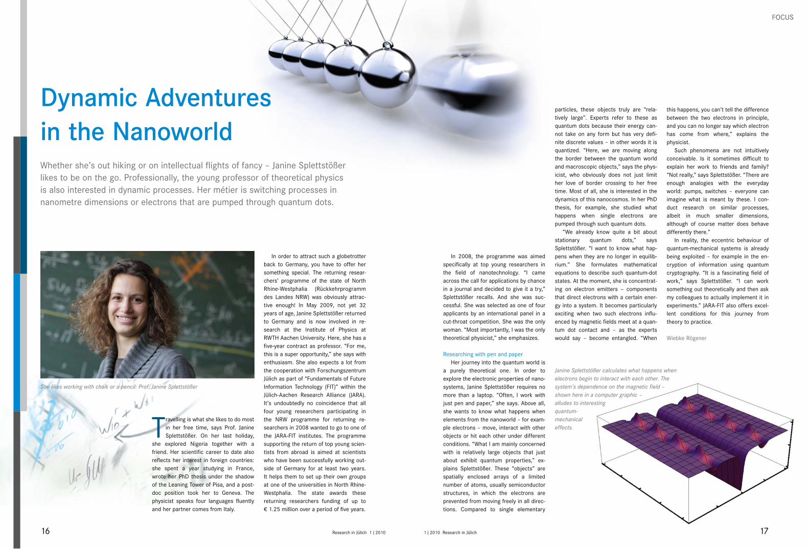
Janine Splettstößer calculates what happens when electrons begin to interact with each other. The system’s dependence on the magnetic field – shown here in a computer graphic – alludes to interesting quantum- mechanical effects.
She likes working with chalk or a pencil: Prof. Janine Splettstößer

Research in Jülich 1 | 201018 1 | 2010 Research in Jülich 19
FOCUS
2
6
8
109
1
Best ProspectsNanoelectronics is a key technology of today, tomorrow and the day after tomorrow. As a result, industrial research is just as sought after as completely new concepts beyond established technology – a promising variety as reflected in these pictures.
1 Magnetic vortices form in wafers that are only a few nano-metres thick. A short pulse of electric current can quickly switch the magnetization inside this vortex – a process shown by this computer simulation.
2 An electron micrograph showing the atomic structure of the high-temperature superconductor YBaCuO. An electronic effect appears here that can be used in what is known as
Hilbert spectroscopy. This method developed at Jülich uses microwaves to quickly and reliably differentiate between different liquids – at security checkpoints for example.
3 Graphic representation of an electrochemical sensor (green with yellow conductors) that detects neurotrans mitter mole-cules. These molecules are secreted by neurons (dark red).
4 Microscopic partial view of a sensor for communication between cells and electronics. The bright blue structures are the same as the yellow structures in Fig. 3.
5 Islets of the semiconductor material germanium have formed in the well-ordered hollows in a silicon wafer, which are between four and eight nanometres deep.
6 Nanocolumns made of gallium nitride as the basic elements for future circuits.
7 Four electrodes (orange) and a nanowire made of indium nitride (bright purple) form a structure that Jülich scientists have investi-gated as a potential component for future quantum computers.
Quantum computers can achieve tremendous speeds thanks to the quantum-mechanical superpositioning and processing of the states in which information is stored.
8 Optical micrograph of a crossbar structure. Jülich scientists have reduced this component to a tenth of its original size for use in future computer storage (see article on page 23). This means that an optical microscope is no longer powerful enough to make the fine structure visible.
9 Neurons (beige) on a field effect transistor.
10 Computer simulation of the electronic structure of a semicon-ductor after the injection of charge carriers with a pre-set spin.
7
5
3
4

Research in Jülich 1 | 201020 1 | 2010 Research in Jülich 21
HIGHLIGHTS
An interview with Prof. Markus Morgenstern and Prof. Detlev Grützmacher
FIT for the Future
Question: Prof. Morgenstern, as JARA-FIT came into being more than two years ago, what did you and your colleagues in Aachen hope to achieve from the alliance with Forschungs-zentrum Jülich? Morgenstern: To even think about work-ing on certain research projects and acquiring funding for the necessary research, you need a certain number of qualified scientists who work in the same area. We hoped to achieve this critical mass, to use a term from physics, through the alliance with Jülich. Another factor was that Forschungszentrum Jülich not only has particularly powerful sci-ence instruments at its disposal, but also the know-how required to use and fur-ther develop them. We therefore expect-ed to profit from this unique strength at Jülich. And finally, we also wanted to cre-ate new opportunities for our students at Aachen, for example, by offering them work placements at Jülich.
Question: And what were the motives behind Jülich’s decision to join forces with RWTH Aachen University in an alli-ance?Grützmacher: In information technology, you have poor prospects as a single insti-tution on the global science market. The issues are very complex and interdiscipli-nary. You need enormous resources to get to the top internationally. This idea of a scientific environment and promising young scientists is exactly what benefits Jülich in this alliance.
Question: With JARA, RWTH Aachen Uni-versity and Forschungszentrum Jülich have embarked on a unique journey to overcome the insularity of university and non-university research. What do you see as JARA’s strength? Grützmacher: JARA is like a marriage. When two people get married, they prom-ise to help and support each other and this involves a certain commitment. Part-nerships without a marriage certificate, in contrast – like cooperations between universities and non-university institu-tions – will not necessarily last for ever. Of course, forced marriages also exist: here pressure is applied from outside on research institutions to amalgamate. I believe the first marriage model to be the best.
Question: Have your expectations been met so far? Morgenstern: Yes. Within JARA-FIT, we have already set up a new research group. Furthermore, JARA-FIT made it possible for us to make a joint applica-tion to the German Research Foundation (DFG) for a collaborative research centre. JARA has been up and running now for two years – a relatively short time but it has already become clear that we will reach the critical mass together and that we will be able to strategically position ourselves better than before. Grützmacher: The vacancies for profes-sors we have recently filled testify to this. Our alliance allowed us to successfully attract prominent scientists with offers that neither Aachen nor Jülich would have been able to make on their own. It also became clear how attractive JARA-FIT is for young researchers. For example, all four nanoscientists selected by the North Rhine-Westphalian programme aiming to attract top young scientists back home from abroad wanted to work with us.
Question: Why should the tax-payers’ money be invested in information tech-nology? Can we not just leave research to industry?Morgenstern: No. Industry is not inter-ested in investigating long-term alterna-tives to established silicon technology for the hardware of the future. For industrial companies, options such as quantum computing or the use of single molecules to transmit information are still too far away from actually meeting the technical specifications of a product. One of the unique things about JARA-FIT is that we pursue this basic research, while also participating in projects aiming to meet the current needs of industry.
In the Jülich-Aachen Research Alliance (JARA), RWTH Aachen University and Forschungszentrum Jülich combine their expertise and capacities to work on complex scientific issues. In the four sections, JARA-BRAIN, JARA-ENERGY, JARA-SIM and JARA-FIT, they decide together what research objectives to pursue, what scientific instruments to purchase and what scientists to appoint. The section known as FIT (Fundamentals of Future Information Technology) has set itself the goal of laying the foundation for the information technology of the future. The directors of JARA-FIT are Prof. Markus Morgenstern, head of II Institute of Physics B at RTWH Aachen University, and Prof. Detlev Grützmacher, director of the Institute of Bio- and Nano-systems at Forschungszentrum Jülich. Together, they take a look back at the strategic partnership to date.
Question: Where do you want to see JARA-FIT in 2015? Morgenstern: There will be a collabora-tive research centre, a joint master’s course, a collaborative graduate school …Grützmacher: ... and a joint infrastruc-ture that will be used for high-perform-ance science. An important step towards this was taken in spring 2009 with the foundation of the Peter Grünberg Centre as a central platform for basic research in the field of nanoelectronics in the region. JARA-FIT will be among the best research institutions worldwide in the field of information technology.
Interview Frank Frick
Prof. Markus Morgenstern (left) and Prof. Detlev Grützmacher, directors of the “FIT” section of the Jülich-Aachen Research Alliance (JARA).

Research in Jülich 1 | 201022 1 | 2010 Research in Jülich 23
Even the most placid of people have been known to lose their patience: all you want to do is have a quick
look at your emails from home or order a cinema ticket online, and booting your computer alone takes what feels like an eternity. The reason for this is DRAM (dynamic random access memory), a main memory module in computers. As the information stored here as electric charges volatilized the last time the PC was turned off, the operating system and all other programmes that are in con-stant use have to be reloaded before the computer can be used. Even when the computer is up and running, DRAM must be reloaded every 60 milliseconds. Data stored on the PC hard drive, in contrast, are permanently available. Here, they are stored in tiny oriented magnetic domains. However, hard drives also have a disad-vantage: they are comparatively slow. Their read and write times amount to thousandths of a second, while DRAMs are ready for use within billionths of a second.
Resistance wanted“My notebook takes a couple of min-
utes to boot at the moment,” says Dr. Carsten Kügeler. What causes despair among others is additional motivation for him. The reason? He is one of the scien-tists from the Institute of Solid State Research at Jülich who are working on a completely new type of storage tech-nique under Prof. Rainer Waser. “The basic principle of our resistive storage is switching the electrical resistance of a material back and forth between a low and a high value,” he explains. Both of these resistance values are then as-signed to the two basic elements in all computer languages – namely “zero” and “one”.
Resistive storage will combine the advantages of hard drives with those of DRAM. The scientists are convinced that it will allow information to be stored with-out any connected mains voltage just like on a hard drive and simultaneously enable information to be written and read just as quickly as with DRAM. As if that
Turbo Storage for the Computers of Tomorrow Up to now, computer memories have involved a choice between two evils: either the data are written and read slowly or the information is lost once the device is switched off. Researchers at Jülich want to change this.
weren’t enough, the new storage ele-ments also require very little space on the computer chip. “This space require-ment is what counts. This causes costs to skyrocket – or indeed to nose dive,” says Kügeler.
A number of groups of scientists from the Institute of Solid State Research are working hand in hand in an effort to real-ize this ambitious goal. The teams head-ed by Prof. Kristof Szot and Dr. Regina Dittmann are pursuing research on the basic physicochemical principles of resis-tive storage. Kügeler’s group is working on adapting the storage concept for inte-gration into existing computer technolo-gy. And among other things, chemist Dr. Rainer Bruchhaus keeps the needs of industry firmly in sight having recently come to Forschungszentrum Jülich from industry.
The first results of this pooling of expertise are excellent. The researchers have proven, for example, that conduc-tive channels are formed in strontium titanate and titanium dioxide – materials
HIGHLIGHTS
A look through the microscope at a disc on which two conductors (yellow) are selectively contacted with two measuring needles (black). The tiny area in the middle of the merging radial conductors is where a novel storage element with 256 resistance channels is located.
Dr. Carsten Kügeler holds a disc with turbo storage.

Research in Jülich 1 | 201024 1 | 2010 Research in Jülich 25
HIGHLIGHTS
that are being studied intensively for use as resistive storage elements – and that their electrical resistance increases rap-idly when a certain threshold voltage is applied. The new higher resistance val-ues remain intact when the voltage is turned off. Only when a corresponding high countervoltage is applied do the channels return to their original low resistance values. This behaviour makes the channels perfect for use as tiny basic elements in memories.
No fundamental obstacles“The channels have a diameter of just
a few nanometres, in other words a few millionths of a millimetre. We can there-fore go right down to this order of magni-tude when designing the smallest struc-tural storage unit,” says Regina Dittmann. However, the size of Kügeler’s basic units, which are used to integrate the resistance channels into the computer periphery, are still much larger than this – namely between 50 and 100 nano metres. But the researchers are optimistic that
there are no fundamental obstacles pre-venting further miniaturization. If they reach a magnitude of 10 nanometres, they will have achieved the objective they set themselves from the start: reducing the space requirements of resistive stor-age elements by a factor of 1000 com-pared to today’s conventional storage elements.
While a base unit in DRAM comprises a condenser, the actual storage element, and a transistor, Kügeler’s base units require nothing other than a resistance channel and electrodes in order to create a link to the “outer world”. Even in the case of the space-hungry electrodes, the scientists have managed to make signifi-cant cuts. Their laboratory prototype comprises 4096 resistance channels, which are arranged in a square with an edge length of 64 channels. Instead of connecting each resistance channel sep-arately to an incoming and an outgoing electrode, the scientists have covered the top outlets of a row of 64 channels with a bar-like vertical electrode. They
have done something similar with the bottom ends of the resistance channels – with a slight difference: the bottom bar electrodes run perpendicular to the top ones. In this way, a crossbar structure is created (see figure) for which only 128 electrodes (64 plus 64) are required. In contrast, 8192 electrodes (2 x 64 x 64) would be needed if each resistance chan-nel was to be coupled separately with an incoming and an outgoing electrode. In spite of this, the crossbar structure also allows a certain number of specific resistance channels to be controlled by applying a voltage to a particular combi-nation of vertical and horizontal elec-trodes. The system is similar to that used to identify a certain field on a chess board by its row and column number.
However, every electronics enthusiast knows that it’s not always that easy in practice. On each electrode, there are also other resistance channels, which are therefore then also live. This gives rise to unwanted parasitic currents. “The strength and appearance of these cur-rents depends on which of the individual resistance channels is switched to zero or one, respectively, at that time,” explains Kügeler. The scientists try to get around this problem by carefully choos-ing the voltage level so as to minimize the parasitic currents. This is not the only problem area that Kügeler’s team are still working on. In the past, the information that was stored in the resistance chan-nels remained saved for around a day. This is actually 20,000 times longer than the storage period in DRAM. “But we still have to improve this by a few orders of magnitude,” admits Kügeler. At the same
time, the researchers are trying to in-crease the difference between the two resistance values represented by zero and one, respectively, in order to improve the reliability of the resistive storage process.
Understanding what happensParallel to Kügeler’s research, Regina
Dittmann’s team is working on under-standing what happens in the resistance channels when they suddenly change their resistance value. “We assume that oxygen ions are moved back and forth when threshold voltages are applied,” says Dittmann. “This allows the material to be switched back and forth from a conducting to an insulating state.” The researcher’s latest findings imply that this theory is indeed correct. While in earlier experiments, the resistance chan-nels lost their switching ability after a certain number of storage cycles, this ability remained unaffected when the sci-entists attached an oxidizable electrode to the surface of the material. Dittmann: “This indicates that the material loses its oxygen ions when this electrode is not
there. The oxide layer on the electrode interface temporarily absorbs the oxygen and then releases it back into the mate-rial during the next switching process.” In this way, explains the physicist, the storage ability of the channels remains intact.
The Jülich researchers, who are work-ing closely together with other groups from RWTH Aachen University as part of the Jülich-Aachen Research Alliance (JARA), agree that it will still take some time before resistive storage is ready for the market. “When we successfully dem-onstrate the basic functionality of the crossbar, then our work here in Jülich is done,” says Rainer Bruchhaus. Dittmann’s and Kügeler’s colleague continues: “Turn-ing the storage concept into a market-able product is no longer basic research; this is a task for industry.” Companies such as Intel are already collaborating with the Jülich researchers today. This is a good sign for these new storage con-cepts. Industry obviously believes them to have good prospects for the future.
Axel Tillemans
Dr. Regina Dittmann conducts research on the basic physicochemical principles of resistance channels, which may be used as tiny basic elements in memories.
This crossbar structure (large image) contains 4096 storage channels but only measures around a hundredth of a milli-metre. Each channel is connected at the top to a horizontal electrode (white in the small image) and at the bottom to a verti-cal electrode (grey); (see also the graphic on the next page).
Each storage channel (red) is connected to the crossbars both at the top and the bot-tom via an electrode bar. By applying volt-age to one of the top and one of the bottom bars, each individual channel can be selectively controlled.

Research in Jülich 1 | 201026 1 | 2010 Research in Jülich 27
HIGHLIGHTS
In 2007, information and communi-cations technologies accounted for around 10 % of the total electricity con-
sumption in Germany. Dr. Daniel Bürgler from the Jülich Institute of Solid State Research explains the global implications of this. “The economic growth of the threshold countries will also cause the global energy requirements for comput-ers to rise rapidly if computers are not made more energy efficient.” However, the conservation of resources and cli-mate protection are not the only reasons for developing less demanding proces-sors: high energy consumption creates so much heat that it simply gets too hot for the sensitive electronics housed in computer cases.
One solution could be spintronics – electronic components that exploit the spin of electrons for information process-ing. However, a number of key questions have yet to be answered. How can a flow
of electrons be produced with just one type of spin? How can the orientation of the spin be manipulated, and how can the orientation of the spin be read out? In order to effectively find answers to these questions, Jülich scientists have designed an instrument that combines multiple functions in one machine: the “Nano-Spintronics Cluster Tool”.
From one station to the nextIn an ultrahigh vacuum that protects
samples from dust and the highly reac-tive oxygen in the air, the scientists first fabricate very thin layers using molecular beam epitaxy. An electron beam evapo-rates the respective starting material. This allows a sample to be constructed atomic layer by atomic layer. In this part of the Nano-Spintronics Cluster Tool, the journey also begins towards creating a component referred to by Jülich physicist Julius Mennig as a “spin valve” because it spatially separates electrons with differ-ent spins.
The Jülich PhD student first produces a basic structure out of non-magnetic conducting copper. Later, layers of mag-netic cobalt are applied to specific strate-gic areas. Without taking the sample out of the protective vacuum, Mennig can push it into the next station of the univer-sal tool. Here, he uses a photoemission
spectrometer and electron diffraction to verify whether the layers are clean and free of defects. Every dust particle, any contact with oxygen or any other contam-inating substance would mean the end of the pro cess at this stage.
Once again, without having to take the sample out of the machine – thus saving time and keeping the sample shielded – the journey continues to an extremely precise cutting tool. Mennig’s valve now
takes on a concrete shape. Using an ion beam with a cutting width of only eight nanometres, the physicist shapes two bars of magnetic cobalt of his minute component. The physicist visually exam-ines the result under the scanning elec-tron microscope, which is also part of the universal tool. “The tool also has a scan-ning tunnelling microscope in another station, which is required just as often for analyses,” explains Daniel Bürgler.
The final test reveals whether the spin valve functions as desired. Still in the uni-versal tool, Mennig sends an electric cur-rent through one of the cobalt bars with the aid of tiny spring contacts. In the magnetized bars, left-handed electrons with a spin that is parallel to the magnet-ism of the bar should advance faster than electrons with an opposing spin. The rea-son for this assumption is that the cobalt atoms already contain the maximum number of left-handed electrons. There is no room for any more in the atoms. A left-handed electron should therefore pass through the cobalt bar almost un-disturbed. On the other hand, the cobalt atoms offer right-handed electrons, whose spin is oriented in the opposite
The Universal ToolOn the search for future energy-efficient information technology, scientists at Jülich create and explore nanoscale components for spintronics. In their quest, they turn to the “Swiss Army knife” among the tools of research: the globally unique “Nano-Spin-tronics Cluster Tool”.
Tradition and the Future: Spintronics in JülichThe scientists Daniel Bürgler and Julius Mennig work in the same institute as the Nobel Laureate Prof. Peter Grünberg who revolutionized data storage on hard drives around 20 years ago with the discovery of giant magnetoresistance. Grünberg’s research laid the foundation for spintronics as a technology of the future. Today, scientists working under Prof. Claus Michael Schneider in the area of “electronic properties” are seeking to gain better control of spin currents and use them for data processing in energy-effi-cient computer components.
direction to the magnetization, numerous free energy states, which hypothetically function like small traps. What percent-age of electrons with the same spin actu-ally ends up in the copper at the end of the bar can be detected by Mennig with the second magnetic bar. Although no electric current flows through this bar, it is possible to measure the electric voltage caused by the electrochemical potential of the electrons separated according to spin.
Spin valve works“We succeeded in conclusively show-
ing that the valve works,” says Mennig
with enthusiasm. However, he doesn’t want to mention any numbers yet. “The whole thing is much more complex than it sounds,” he admits. “The bars, which are only 200 nanometres away from each other, sometimes influence each other’s magnetic orientation – and this makes it more difficult to control the direction of the spin.” Despite this, the spintronics researchers are confident that they will be able to quickly overcome this problem with the aid of their universal tool and thus provide the impetus for information technology in the future.
Brigitte Stahl-Busse
Viewing windows allow a glimpse into the inside of the Nano-Spintronics Cluster Tool (left) – and also, for example, into the silver sample carousel with space for up to six samples (below).
Recognizable only under an electron micro-scope: the “spin valve” of a few microme-tres in size. The non-magnetic conducting copper structures gleam brightly. The two vertical magnetic cobalt pins appear some-what darker in the image.

Research in Jülich 1 | 201028 1 | 2010 Research in Jülich 29
HIGHLIGHTS
NanosonarSonar sends out sound waves which are used to explore the depths of the ocean. As Jülich scientists discovered, a similar principle allows the flow of electrons in a scanning tunnelling microscope to be used to investigate the hidden properties of the atomic lattice of metals.
Important discoveries are often the work of researchers who dedicate themselves to studying phenomena
that others have left by the wayside. “When using scanning tunnelling micro-scopes to investigate the surfaces of solids, a whole range of scientists have noticed spherical patterns,” says Dr. Samir Lounis. The theoretical physicist
at the Jülich Institute of Solid State Research continues: “It is a well-known fact that foreign atoms inside the mate-rial being studied can cause these rings.” However, in contrast to other scientists, Lounis and his colleagues Prof. Stefan Blügel and Prof. Peter Dederichs did not just see an annoying interference caused by impurities but a source of information on the internal structure of crystals. Decisive information was provided by sci-entists from Göttingen, who conducted new experiments.
Informative wavesIn order to understand the delibera-
tions of the Jülich scientists, it is impor-tant to know the following: a scanning tunnelling microscope images a surface by tracing this surface with a tip. During this process, electrons tunnel from the tip to the surface. These electrons spread out like waves in the solid, following the laws of quantum mechanics. Like waves in water, they are scattered when they hit an obstacle or they are reflected and par-tially thrown back up to the surface. The
reflected electron waves therefore con-tain information on the inside of a solid – similar to the reflected sound waves emitted by sonar, which provide informa-tion on the nature of the seabed.
But what do these patterns actually look like? For example, what patterns are generated on the surface of copper by a cobalt atom embedded within the cop-per? The Jülich scientists quickly realized where they should look for the answer: in what are known as Fermi surfaces. “These constructions, which are not located in normal space but rather in a mathematically derived space, determine the electronic, magnetic, optical and thermal properties of metals and semi-conductors. They therefore provide a sort of profile for a material,” says Stefan Blügel. The Fermi surfaces of a copper atom also determine how electrons – or to be more exact the electron waves – spread out in copper. “The electrons travel along certain roads, the direction and size of which are determined by the Fermi surfaces,” explains Lounis. “On some of these roads, the electrons travel at top speed, like cars on a motorway, while on others, they crawl along as if they were travelling on a dirt track.”
The researchers therefore faced the task of using the known Fermi surfaces for copper in order to work out the “road map” for copper containing a deep impu-rity in the form of a cobalt atom. Although the physicists limited themselves to a piece of copper measuring only a few millionths of a millimetre, they still required the concentrated power of the Jülich supercomputer JUMP for the com-plex quantum physics calculations.
The result: for the most part, “dirt tracks” run from the foreign atom. How-ever, the electrons travelled at speed in some directions – as if they were on a motorway. In areas where the “motor-ways” penetrated the copper surface, patterns were visible. However, the cal-culations made by the Jülich physicists did not yield circles; they yielded rounded triangles that closely resembled rings. The very same triangles were also found by scientists in Göttingen who conducted high-precision experiments with copper samples doped with cobalt atoms.
Pioneering resultsThe Fermi surfaces are very well
known for pure materials, such as cop-per. This is different in the case of alloys, which can be composed of all sorts of combinations of single chemical ele-ments. “Our results point the way towards a technique that can be used to determine at least parts of these previ-ously unknown Fermi surfaces,” Lounis is happy to report. The scanning tunnelling microscope studies of a surface can also be used to determine the exact position of a foreign atom in the depths of a metal.
Lounis is certainly not short of ideas for further possible applications of the new theoretical information: “In the future, we could perhaps save informa-tion in atoms that are located deep below the surface.” To do so, electrons could be sent along “motorways” with a scanning tunnelling microscope leading directly to the corresponding atom in order to reverse the spin of one of its electrons. As the spin can assume two states (“up” and “down”), it is suitable for storing infor-
mation. “This would make all other stor-age techniques look antiquated in com-parison,” says Lounis with conviction.
Axel Tillemans
Top: Rings recorded by the scanning tun-nelling microscope that appear due to for-eign atoms under the surface. Only when the image is very precisely analysed does it become clear that these structures are actually round triangles. Bottom: Computer simulation of the structures.
The Fermi surface of copper, where the colours make the cur-vature clearer. Where the Fermi surface is particularly flat (red), the electrons travel particularly fast through the solid. The Fermi surfaces provide, so to speak, the profile of a metal or a semi-conductor.

Research in Jülich 1 | 201030 1 | 2010 Research in Jülich 31
Tricks for Faster TransistorsJülich researchers have developed methods that allow the crystal lattice of silicon to be expanded. This strained silicon can then be used to fabricate transistors for computer chips that work much faster than the conventional technology.
HIGHLIGHTS
On a square centimetre of today’s computer processors, up to two billion tiny on and off switches –
transistors – fight for space. Making them even smaller is one way of making computers even faster in the future. However, there is one other option. In the silicon structure of a transistor, the charge carriers flow from A to B. A simple
Mantl. The German Federal Ministry of Education and Research is funding the project with a total of € 8.1 million. A further € 6.4 is being provided by the collaborative partners Globalfoun-dries Dresden, Siltronic AG, Aixtron AG, Forschungszentrum Jülich and the Max Planck Institute of Microstructure Physics.
The silicon wafers used in industry as substrates for circuits and transistors typically have a diameter of 300 milli-metres. The Jülich researchers have as-certained that a 1% expansion of the crystal structure would be optimal at such magnitudes. The wafers do not bend and the transistors are 20 to 30% faster on average than conventional components.
Getting to the pointA somewhat different approach is fol-
lowed by the team headed by Prof. Detlev Grützmacher, director of the Jülich Insti-tute of Bio- and Nanosystems. He works
closely with Europe’s largest semicon-ductor manufacturer STMicroelectronics and concentrates on wafers on which islets of strained silicon are distributed like a host of tiny dots. To fabricate such wafers, the scientists first etch millions of holes in the wafers at regular intervals, each of which is between four and eight nanometres deep. They then deposit pure germanium on the wafer. Capillary action causes the germanium to collect in these holes and little domed islets are formed. The researchers then deposit a layer of silicon over the surface of the wafer as though covering it with a thin cloth. Wherever a germanium islet is cov-ered by the “cloth”, there is a local bulge in the silicon layer. When the Jülich scien-tists remove the germanium again in an-other step, they are left with both highly conductive as well as highly insulating silicon bridges. “We have already used these wafers to fabricate transistors that are 15 to 30% faster than components that are not strained,” reports Grütz-macher enthusiastically.
Whether sheet-like or dotted strained silicon will come out on top in the end is hard to say today. “We have made sure that both methods create a transistor
that is compatible with today’s produc-tion techniques,” emphasizes Grützmach-er. Production conditions are indeed very demanding in the semiconductor indus-try. Huge importance is laid on perfect structures and layers, dust-free systems and products, and automation. After all, a company must be able to guarantee that all two billion transistors in a processor will run without any problems.
In order to work at industry level, Jülich scientists have access to a clean room, four coating units and a new wafer cleaning system for 300-mm wafers. The equipment and know-how of scientists who have worked in industry guarantee the fabrication of structures and inter-faces with an extremely high degree of purity and perfection. Detlev Grützmacher and Siegfried Mantl are convinced that the silicon era in information technology is only just beginning: “Before new tech-nologies can be realized, the future will first belong to new material combinations that will all have one thing in common: silicon,” says Mantl.
Brigitte Stahl-Busse
trick can speed up this flow of charge. If the crystal lattice of the silicon is strained, the charge carriers will move faster.
Germanium as a stretching aidThe team headed by Prof. Siegfried
Mantl at the Jülich Institute of Bio- and Nanosystems stretches the crystal lattice using a trick. The scientists exploit the natural difference in the crystal structure of silicon and germanium. The atoms in both materials are ordered in the same way but the interval at which they occur is 4.2% greater in germanium than in sili-con. If a thin layer of silicon measuring around ten nanometres is grown on a pure germanium layer with a thickness of some hundred nanometres, the crystal lattice of the thinner layer adapts in line with the thicker layer. The result: the crystal lattice of silicon is stretched in planes parallel to the surface by a few percent. By using different germanium-silicon alloys in the thick layer instead of pure germanium, the researchers can even set different strains in the thin layer.
“Our objective is to achieve as even and defect-free a strained silicon layer as possible over a very large area,” says Dr. Bernhard Holländer who works with
Capillary action ensures that the germa-nium islets appear homogeneous and well ordered. The strong magnification shown in the top right-hand corner clearly shows how homogeneous the islets actually are.
On the far right of the above image, a present-day 300-millimetre wafer is shown. On the far left, a silicon wafer with a diameter of 100 millimetres is pictured, representing the industrial standard around 30 years ago.

Research in Jülich 1 | 201032 1 | 2010 Research in Jülich 33
HIGHLIGHTS
The numerical sequence 1000001 1000010 1000011 represents the letters “ABC” – at least according to
the widely used American Standard Code for Information Interchange, also known as ASCII code. In actual fact, all types of information can be expressed as a sequence of zeros and ones. But how are the two states “zero” and “one” written to electronic storage material and perma-nently stored? In the case of electronic storage, which we come across everyday for example in smart cards and electronic
field,” says Prof. Knut Urban, one of the two directors of ER-C. The oxygen ions are very slightly displaced by around 20 picometres (1 picometre is equal to a bil-lionth of a millimetre, which corresponds to less than a hundredth of an atomic diameter). “Even just a few years ago, nobody would have believed that such displacements could be measured with the precision of a few picometres,” says Urban. Working together with research-ers from Darmstadt and Heidelberg, the Jülich physicists successfully developed an electromagnetic correction element in
the 1990s, which is used to correct strong aberrations in the objective lenses of electron microscopes in much the same way as glasses. Up to this point in time, these optical aberrations had greatly restricted the attainable sharpness and resolution of electron microscopes.
The next stepEquipped with such correctors, com-
mercial electron microscopes are now capable of resolving atomic structures. In the complex task of adjusting the correc-tors, measuring techniques and compu-
ter programmes from Jülich, which have been licensed by the electron-optical in-dustry, are used. “Despite this, the tech-nical effort and the know-how required to generate such images are immense, and the requirements to be observed in fabri-cating preparations with a thickness of only a few atomic layers are stringent,” says Prof. Joachim Mayer, the second director of ER-C. The physicist from RWTH Aachen University continues: “The neces-sary performance of instruments and personnel can only be achieved if univer-sities and non-university research institu-tions combine their efforts in a joint facil-ity like ER-C.” The next step towards maintaining their position among the world leaders in electron microscopy has already been made: at the end of 2009, the first cut of the spade was made for an extension to ER-C. The extension will house the new supermicroscope PICO with a resolution that is almost double that of currently available instruments. At the same time, PICO will increase the precision with which scientists can measure atomic distances and atomic displacements from five picometres to a single picometre. “This will bring us to the physical limits of optics,” says Urban. However, this is not an end in itself, emphasizes Urban. “In order to be able to control and optimize the components in nanoelectronics and nanotechnology, we must be able to analyse them in the picometre range.”
Frank Frick
Unique Insight into the World of AtomsWith the electron microscopes at the Ernst Ruska Centre (ER-C), nanoelectronic materials can be studied – atom position by atom position. The supermicroscope known as PICO will move to ER-C in 2010. It measures atomic displacements with an accuracy of one picometre or a billionth of a millimetre. And that’s a world record!
car keys, this question can meanwhile be answered very precisely. And not just with abstract words. Thanks to scientists at the Ernst Ruska Centre for Microscopy and Spectroscopy with Electrons (see info box), this can be done in such a way that changes in the atomic lattice of the storage material are made visible in an image, thus making them easy to see for everyone.
20 picometres make the differenceFerroelectric materials are perma-
nently electrically polarized: in contrast to most chemical compounds, the centre of the positive and negative charge does not coincide on an atomic level – even when there is no external electric field. The reason for this polarization in oxidic ferroelectrics is that the negatively charged oxygen ions in the crystal lattice are not located exactly in the middle of two positively charged metal ions. Such materials are suitable for use as storage media because the direction of their polarization can be reversed with an ap-plied external electric field. This switch-ing always occurs in very small zones known as domains in technical jargon. Domains with a polarization in one direc-tion therefore correspond to the state “zero”, while domains polarized in the opposite direction have the state “one”.
Ernst Ruska Centre (ER-C)ER-C was founded in 2004 as a joint platform of excellence by Forschungszentrum Jülich and RWTH Aachen University. It functions as a national user centre for atomic-resolution electron microscopy and spectroscopy. Today, ER-C is the top institution in-ternationally in this field. It is operated under the auspices of the Jülich-Aachen Re-search Alliance (JARA) and its premises are on the Jülich campus. ER-C receives grants from the German Research Foundation (DFG) as well as the federal government and the federal state. Half of the centre’s measuring time is allocated to researchers from universities and industry both in Germany and abroad.
Every bit of information can be expressed as a sequence of the states “zero” and “one”. This electron micrograph shows how the position of oxygen ions in a material changes when information is written to the material.
“In our electron micrographs, we can see for the first time how the oxygen ions change their position in the crystal lattice when information is written to the mate-rial with the aid of an external electric

Research in Jülich 1 | 201034 1 | 2010 Research in Jülich 35
HIGHLIGHTS
News all about information technology
At the beginning of 2009, the central platform for basic research in the field of nanoelectronics in the Jülich-Aachen region came into being: the Peter Grünberg Centre. Forschungs-zentrum Jülich named the centre in honour of its Nobel Laureate, physicist Prof. Peter Grünberg. The research centre is rooted in the cooperation with RWTH Aachen University, namely the Jülich-Aachen Research Alliance (JARA). It is the first institution in the field of nanoelectronics throughout Germany that is also open to external users.
New Platform
A German-Japanese research team with the major involvement of Jülich scientists succeeded in conclusively clarifying the long contested structure of a material that is used in DVDs and other optical data storage media. This material can be switched be-tween two different states: a regular crystalline state and a more irregular “amorphous” state. We now know why this switching occurs on an atomic level, and can begin looking for better storage materials. The structure was decoded thanks to techniques such as simulations on the Jülich supercomputer known as JUGENE.
Decoded Structures
In the journal Science, researchers from Mainz, Cologne and Jülich reported on a new model system composed of ultracold atoms that can be used to study the behaviour of electrons in a solid. In this system, the atoms are trapped in an optical lattice created by superimposing a number of laser beams. Supported by simulations at the Jülich Supercomputing Centre, the scien-tists were able to use this experimental procedure to explain a spectacular phenomenon whereby a metal abruptly loses its conductivity when the interaction between electrons becomes too strong.
Ultracold Model
Researchers from Jülich, Kaiserslautern and the USA have devel-oped a new method to track ultrafast magnetic processes that are decisive for the write speed of future magnetic data storage media. The basis for the method is a femtosecond laser whose flashes of light are directed into the noble gas neon. This cre-ates weak X-ray pulses, which are only around ten femtosec-onds (ten quadrillionths of a second) long. If they hit a sample, the resulting diffraction patterns can be used to derive conclu-
Ultrafast Measurements
In 2010, work will begin in Jülich on the construction of the Helmholtz Nanoelectronic Facility (HNF), a state-of-the-art re-search and development facility in the field of nanoelectronics. The plans include clean rooms that are up to 10,000 times cleaner than operating theatres in hospitals. They will be equipped with instruments – including an epitaxy and nanofabri-cation cluster – that will make HNF a unique facility in Europe. The cluster comprises a continuous production facility measur-ing six metres by fifteen, which will be used initially to fabricate artificial crystal structures and subsequently to produce circuits on a nanoscale.
State-of-the-Art Clean Room Centre
PUBLICATION DETAILS
sions on their properties. The advantages of the method, which does not require a large-scale facility, include extremely fine tem-poral resolution and a spatial resolution in the nanometre range.
Research in Jülich Magazine of Forschungszentrum Jülich, ISSN 1433-8514 Published by: Forschungszentrum Jülich GmbH | 52425 Jülich | Germany Conception and editorial work: Dr. Frank Frick, Dr. Anne Rother (responsible according to German press law), Kosta Schinarakis Authors: Dr. Wiebke Rögener, Dr. Frank Frick, Dr. Axel Tillemans, Brigitte Stahl-Busse Design and Layout: Graphical Media, Forschungszentrum Jülich Translation: Language Services, Forschungszentrum Jülich Photos: Forschungs zentrum Jülich (cover illustration, pp. 2 – 4, pp. 7 – 15, p. 16 bottom left, pp. 18/19, pp. 22 – 27, p. 28 top, p. 29, p. 30 bottom, p. 31 bottom, p. 33, p. 34 top right, p. 35 top left), Hermes Verbund (p. 6 top left), Fotolia (p. 6 top right, p. 16 top, p. 28 middle, p. 34 bottom), Mauritius (p. 20, p. 35 bottom), AMD (p. 30 top), Siltronic (p. 31 top), FEI Company (p. 32), RWTH Aachen (p. 17 bottom), Martin Lux (p. 21), Max-Planck Institute for Quantum Optics (p. 34 top left) Contact: Corporate Communications |
Telephone +49 2461 61 - 4661 | Fax +49 2461 61 -4666 | [email protected] Printed by: Schloemer und Partner GmbH Print run: 2,500
Scientists from Jülich and Slovenia have demonstrated that digital data can also be recorded without an electric or mag-netic field. They saved one byte of information in structurally complex solids in which the atomic magnetic moments were unable to assume a ground state. To achieve this, they continuously cooled the samples right down to very low temperatures, taking defined breaks in between, during which they kept the temperature constant. This created a characteristic readable arrangement of magnetic moments in the solid. A patent application has been filed for the new storage principle, which could prove extremely useful in very different fields: in secure data transfer for example or the analysis of dust from space.
Cold Storage

Member of:
Related Documents