Materials Science and Engineering B 134 (2006) 118–124 Nanocrystalline silicon films as multifunctional material for optoelectronic and photovoltaic applications S. Pizzini a,∗ , M. Acciarri a , S. Binetti a , D. Cavalcoli b , A. Cavallini b , D. Chrastina c , L. Colombo d , E. Grilli a , G. Isella c , M. Lancin e , A. Le Donne a , A. Mattoni d , K. Peter f , B. Pichaud e , E. Poliani a , M. Rossi b , S. Sanguinetti a , M. Texier e , H. von K¨ anel c a Dipartimento di Scienza dei Materiali, Universit` a di Milano-Bicocca,Via Cozzi 53, Milano, Italy b Dipartimento di Fisica, Universit` a di Bologna, Viale Berti-Pichat 6a, Bologna, Italy c L-NESS, Dipartimento di Fisica del Politecnico di Milano, Polo Regionale di Como, Via Anzani 52, Como, Italy d INFM-SLACS Sardinian Laboratory for Computational Materials Science, Department of Physics, Universit` a di Cagliari, Cittadella Universitaria, Monserrato (Ca), Italy e Universit´ e Paul C´ ezanne, Laboratoire TECSEN, Facult´ e des Sciences et Techniques de St J´ erome, Marseille, France f Universit¨ at Konstanz, Department of Physics, Universit¨ at Strasse, Konstanz, Germany Received 5 May 2006; accepted 27 June 2006 Abstract Nanocrystalline silicon (nc-Si) already attracted a considerable attention as a promising material for photovoltaic applications, while its full opto- electronic potentiality is still under investigation, due to the relatively poor knowledge of the correlations between growth conditions, microstructure and physical properties. This paper aims at the illustration of the preliminary results of a 3 years project, addressed at the demonstration of the multifunctionality of nanocrystalline silicon, via the understanding of the quantitative correlations between growth process parameters and the structural, optical, electrical and physico-chemical properties of nc-silicon. The main topics foreseen and actively pursued were: • The development of a gas phase kinetic model to be used for the simulations of the plasma enhanced chemical deposition (PECVD) process, the development of a kinetic model relative to the interaction of radicals present in the plasma phase at the substrate interface, and last but not least, the development of models relative to the subsequent nc-Si growth. • The growth of undoped and doped nc-Si layers on convenient substrates by the low energy plasma enhanced chemical deposition (LEPECVD) process using silane, phosphine, diborane and hydrogen mixtures. • The quantitative experimental determination of the correlation among the crystallinity fraction, the film microstructure, the grain size/shape/orientation, the hydrogen content, the density of the recombination centres, the optical absorption coefficient the strain/stress state and the carrier mobility and diffusion length in undoped and n-type and p-type films, in view of the optimization of the minority carrier generation and carrier collection. The preliminary results already demonstrate that a proper modelling of the growth process is of great help in the selection of optimised growth procedures for nc-Si films and that a full range experimental characterisation is needed to get the proper inputs to the modelling activity. © 2006 Elsevier B.V. All rights reserved. Keywords: Nanocrystalline silicon; Modelling; Structure; Crystallinity; Optoelectronic properties ∗ Corresponding author. Tel.: +39 02 64485135; fax: +39 02 64485400. E-mail address: [email protected] (S. Pizzini). 1. Introduction It is well known that nanocrystalline silicon (nc-Si) is consid- ered a promising candidate for low cost and high efficiency solar cells [1,2], having already reached in lab tests top efficiencies 0921-5107/$ – see front matter © 2006 Elsevier B.V. All rights reserved. doi:10.1016/j.mseb.2006.06.038

Welcome message from author
This document is posted to help you gain knowledge. Please leave a comment to let me know what you think about it! Share it to your friends and learn new things together.
Transcript
A
ea
oe
•
•
•
p©
K
0d
Materials Science and Engineering B 134 (2006) 118–124
Nanocrystalline silicon films as multifunctional material foroptoelectronic and photovoltaic applications
S. Pizzini a,∗, M. Acciarri a, S. Binetti a, D. Cavalcoli b, A. Cavallini b, D. Chrastina c,L. Colombo d, E. Grilli a, G. Isella c, M. Lancin e, A. Le Donne a, A. Mattoni d,
K. Peter f, B. Pichaud e, E. Poliani a, M. Rossi b, S. Sanguinetti a,M. Texier e, H. von Kanel c
a Dipartimento di Scienza dei Materiali, Universita di Milano-Bicocca,Via Cozzi 53, Milano, Italyb Dipartimento di Fisica, Universita di Bologna, Viale Berti-Pichat 6a, Bologna, Italy
c L-NESS, Dipartimento di Fisica del Politecnico di Milano, Polo Regionale di Como, Via Anzani 52, Como, Italyd INFM-SLACS Sardinian Laboratory for Computational Materials Science, Department of Physics,
Universita di Cagliari, Cittadella Universitaria, Monserrato (Ca), Italye Universite Paul Cezanne, Laboratoire TECSEN, Faculte des Sciences et Techniques de St Jerome, Marseille, France
f Universitat Konstanz, Department of Physics, Universitat Strasse, Konstanz, Germany
Received 5 May 2006; accepted 27 June 2006
bstract
Nanocrystalline silicon (nc-Si) already attracted a considerable attention as a promising material for photovoltaic applications, while its full opto-lectronic potentiality is still under investigation, due to the relatively poor knowledge of the correlations between growth conditions, microstructurend physical properties.
This paper aims at the illustration of the preliminary results of a 3 years project, addressed at the demonstration of the multifunctionalityf nanocrystalline silicon, via the understanding of the quantitative correlations between growth process parameters and the structural, optical,lectrical and physico-chemical properties of nc-silicon. The main topics foreseen and actively pursued were:
The development of a gas phase kinetic model to be used for the simulations of the plasma enhanced chemical deposition (PECVD) process,the development of a kinetic model relative to the interaction of radicals present in the plasma phase at the substrate interface, and last but notleast, the development of models relative to the subsequent nc-Si growth.The growth of undoped and doped nc-Si layers on convenient substrates by the low energy plasma enhanced chemical deposition (LEPECVD)process using silane, phosphine, diborane and hydrogen mixtures.The quantitative experimental determination of the correlation among the crystallinity fraction, the film microstructure, the grainsize/shape/orientation, the hydrogen content, the density of the recombination centres, the optical absorption coefficient the strain/stress state andthe carrier mobility and diffusion length in undoped and n-type and p-type films, in view of the optimization of the minority carrier generationand carrier collection.
The preliminary results already demonstrate that a proper modelling of the growth process is of great help in the selection of optimised growthrocedures for nc-Si films and that a full range experimental characterisation is needed to get the proper inputs to the modelling activity.
2006 Elsevier B.V. All rights reserved.
ectron
eywords: Nanocrystalline silicon; Modelling; Structure; Crystallinity; Optoel∗ Corresponding author. Tel.: +39 02 64485135; fax: +39 02 64485400.E-mail address: [email protected] (S. Pizzini).
1
ec
921-5107/$ – see front matter © 2006 Elsevier B.V. All rights reserved.oi:10.1016/j.mseb.2006.06.038
ic properties
. Introduction
It is well known that nanocrystalline silicon (nc-Si) is consid-red a promising candidate for low cost and high efficiency solarells [1,2], having already reached in lab tests top efficiencies
and E
aaevs(
abat
paeapsd
cgc[ct
tdcatdlsbbioioitusp
at
S
wrtru
Sbcaafi
edn
2
tiapitttseie
atwocnmcb
atyaprcdtlaasTwa
S. Pizzini et al. / Materials Science
round 11%, comparable with those obtained using stabilizedmorphous silicon (a-Si) [3]. It is also known that nc-Si is gen-rally prepared via variants of the plasma enhanced chemicalapour deposition (PECVD) and might be described as a bipha-ic material consisting of a dispersion of silicon nanocrystalsnc-Si) embedded in a matrix of amorphous silicon (a-Si).
The a-Si matrix should present the typical disorder of anmorphous material, i.e. the presence of dangling and distortedonds in its bulk and at the interface with the crystalline grains,ccompanied by local strain set-up, due to their different densi-ies and thermal expansion coefficients.
In spite of disorder, which might be at least partially sup-ressed by hydrogenation [4], this kind of structure looks veryppealing not only for solar cell applications, but also for opto-lectronic applications, as it mimics a dispersion of Si dots inmatrix of a-Si characterized by a larger energy gap, and thenotentially inducing quantum confinement effects, provided oneucceeds in reducing the size of the crystallites to few nm iniameter.
Notwithstanding these potential merits, the industrial appli-ations of nc-Si are limited, at present, by the relatively lowrowth rate typical of most PECVD processes [5] and the diffi-ulty of a proper tuning of the nanomorphology of the material6], in view of optoelectronic applications, where the size ofrystalline silicon dots and the interfacial stress/strain condi-ions play a critical role.
Recently, however, it has been shown that by the use ofhe very high frequency glow discharge (VHFGD) technique,eposition rates of the order of 1–3 nm/s can be obtained [7],ompatible with industrial applications. This rate target has beenlso achieved in some preliminary experiments carried out withhe use of the low energy plasma enhanced chemical vapoureposition (LEPECVD) system [8] in which a dense plasmaeads to very efficient cracking of gaseous precursors, such asilane, which, together with intense bombardment of the surfacey low-energy ions. As a result, growth rates up to 10 nm/s haveeen achieved in the epitaxial growth of SiGe alloys. Concern-ng the problem of controlling and tuning the nanomorphologyf the material, there is the need of developing computer model-ng procedures, as the nanocrystals size and the volume fractionf nc-Si in a-Si are shown to depend in a very complex fash-on on the silane/hydrogen ratio, the deposition temperature,he growth rate, and the plasma energy. This makes difficult tonderstand the correlations between preparation conditions andtructural and physical properties of nc-Si by purely empiricalrocedures.
In fact, the chemistry of deposition process could be formallyccounted for, according to Veprek [9], by the following equa-ion:
iH4plasma−→ [SiHn]
r1�r2
nc/a-Si : H + m[H2]
here r1 and r2 represent the forward and backward reaction
ates, [SiHn] represents the radical or ionic species present inhe plasma, H2 the hydrogen evolved and trapped in the mate-ial as molecular hydrogen and Si:H is the hydrogen bonded tonsaturated silicon atoms in a-Si or at the interfaces between a-aAar
ngineering B 134 (2006) 118–124 119
i and nc-Si. However, it is not so obvious how the volume ratioetween nc-Si and a-Si and the nc-Si crystallites size could beontrolled. This is because the rate of formation of nc-Si versus-Si depends on reactions occurring both in the plasma phasend at the interface between the plasma phase and the growinglm.
For this reason the active interplay between growing, mod-lling and characterization activities is the key issue for theefinitive understanding of the properties and potentialities ofc-Si.
. Modelling studies
A preliminary, but necessary, step towards the modeling ofhe complex processes occurring during the growth of nc-Sis represented by the capability to generate reliable models ofmorphous silicon, a-Si, silicon nanocrystals, nc-Si, and mixedhase nc-Si/a-Si silicon systems. To this aim molecular dynam-cs simulations were performed, based on empirical potentialhat make affordable large systems (up to 106 atoms) necessaryo reach the length scale of several nanometers. Our inves-igation was focused on the relevant case of nanocrystallineystems formed by columnar (or pseudo columnar) grains ori-nted orthogonally to the plane of the substrate as experimentallydentified in LEPECVD-grown thin films in previous and actualxperiments (see next sections).
In order to generate reliable amorphous/crystal interfacesdvantage was taken of the spontaneous recrystallization fromhe amorphous phase that occurs at suitable high temperatureshen crystalline seeds are present [10]. To this aim was devel-ped an efficient and fully-scalable molecular dynamics (MD)ode for large scale simulations [11], as well as a novel library ofumerical tools aimed at inserting crystallites into an amorphousatrix. Atomic forces were calculated according to the empiri-
al EDIP potential that nicely reproduces the bulk properties ofoth crystalline and disordered silicon phases [12].
The starting point of present protocol was to generate anmorphous slab by quenching a liquid silicon sample to roomemperature (see Figs. 1 and 2). The slab dimensions along the x,and z Cartesian axes were 2.71, 27.11, 27.11 nm, respectivelynd the system was periodically replicated. A given number ofarallel fibers were cut off a suitable silicon monocrystal andandomly inserted into the amorphous slab. The axes of therystalline fibers were chosen along the [0 0 1] crystallographicirection and parallel to the x direction of the cell. Furthermore,he fibers radii were small enough so as to avoid fibers over-apping. In the orthogonal y–z plane the fibers were rotatedt random and eventually the atomic forces were relaxed bydamped dynamics minimization method. A plane view of a
elected part of the system (in the y–z plane) is reported in Fig. 1.he cylindrical grains are embedded into the amorphous net-ork and the system exhibits disorder in both the size (2–4 nm)
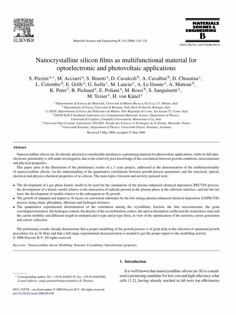
nd the orientation of the crystallites. The system was annealed
t 1200 K in order to thermally activate the recrystallization.fter 2 ns long annealing a stationary configuration was obtainednd is reported in Fig. 2. The amorphous matrix is dramaticallyeduced and extend over a thin region (of the dimension of few
120 S. Pizzini et al. / Materials Science and E
Fii
aotsopodtcaic
Fnr
3
iw(
aotaaasrd(
potdo
4
app
ig. 1. Snapshot showing the starting model nc-Si/a-Si system formed by insert-ng a random distribution of nm-sized crystallites (dimension 2–4 nm) embeddednto an otherwise amorphous matrix.
tomic layers) localized at the grain boundaries. The dimensionf grains depends on the initial density of crystallites and inhe present case ranges within 4–15 nm. The shape and dimen-ion of the grains is determined by several factors: the interplayf neighboring grains, the initial stress in the fibers, the tem-erature of the annealing and the fact that grain recrystallizationccurs preferentially along the [1 1 0] direction. Present analysisemonstrates that it is possible to generate mixed nanocrys-alline columnar models by controlling the disorder of the initial
rystallites but without the need of any initial guess about the-Si/c-Si interface. This is clearly demonstrated by the fact that,n the final grains structure, there is no memory of the initialylindrical shapes.ig. 2. After 2 ns annealing at 1200 K recrystallization gives rise to a texturedc-Si system. The residual amorphous ratio corresponds to a thin intergranularegion as large as few atomic layers.
porX
dcwttn
uat
wa0
0tPiP(
ngineering B 134 (2006) 118–124
. Growth of nc-Si films
The apparatus described in a former paper [13] has beenmproved with the set-up of a second deposition chamber (LG2)hich accepts 8 in. wafers, in addition to the original chamber
LG1), accepting only 4 in. wafers.Two sets of samples were prepared, one set with the LG1,
nd the other set with the LG2, both consisting of a filmf nc-Si approximately 1 �m thick, deposited at dilution fac-ors d = Φ(SiH4)/[Φ(SiH4) + Φ(H2)] between 1% and 10% with
substrate temperature ranging from 210 to 280 ◦C, which,ccording previous work carried out by some of the presentuthors, presented structural and electronic properties of sub-tantial interest for optoelectronic applications. In fact, dilutionatios lower than 10% were shown to be appropriate for pro-ucing material with a crystallinity fraction χc of roughly 70%according to Raman measurements).
One additional set, to be used as reference for a-Si, has beenrepared using dilution factors of 50–100%. The main featuresf the samples prepared are reported in Table 1, where alsohe grain sizes L in a particular crystallographic direction areisplayed. As substrates, Czochralski (CZ) silicon and thermallyxidized CZ wafers were systematically used.
. nc-Si film characterization: generalities
The main scope of the characterization work was to collectfull amount of information about the structural, chemical andhysical properties of samples prepared, to be used as inputarameters for the modeling work and for a further samplereparation campaign. Structural characterization was carriedut using transmission electron microscopy (TEM) and highesolution-TEM (HRTEM), atomic force microscopy (AFM),-ray diffraction (XRD) and Raman spectroscopy.AFM has been used in contact mode for topography and con-
uctive atomic force microscopy analyses [14] using a commer-ial apparatus (NT-MDT, Solver-Pro). The topography resultsere compared with TEM analyses, while c-AFM has been used
o achieve, on a microscopic scale, information on the conduc-ion mechanism through the grain and/or at the border of theanostructures.
The optoelectronic characterization has been carried outsing surface photovoltage spectroscopy (SPS) analyses [15]nd photoluminescence (PL) measurements for the determina-ion of the optical gap and for defect states spectroscopy.
The experimental apparatus for SPS analyses, described else-here [16], allows for the measurement of the surface photovolt-
ge signal in non contact mode, in a wide spectral range (from.6 to 2 eV).
PL measurements were performed at low T (15 K) in the.4–2.2 eV range. The detection of the infrared part of the spec-
rum required the use of FFT spectrometer equipped with abS detector. A back-illuminated CCD coupled with a grat-ng monochromator has been used for the visible range. TheL excitation was performed via a Nd:YAG duplicated laserλexc = 532 nm).
S. Pizzini et al. / Materials Science and Engineering B 134 (2006) 118–124 121
Table 1Preparation conditions and main physical properties of the nc-Si samples
No. Substrate Ts (◦C) d (%) L〈111〉 (nm) L〈220〉 (nm) L〈311〉 (nm) χc (%) σd at RT (�−1 cm−1) Ea (eV) σf (MPa)
6731 SiO2/Si (1 1 1) 250 4.2 – 13 16 75 3.7e−6 0.436733 SiO2/Si (1 1 1) 280 2 – 15.7 20.7 77.5 7.6e−6 0.436956 Si (0 0 1) 230 4.2 18.1 10.7 12 75 – –7365 Si (0 0 1) 210 4.2 22.5 20.5 16.6 73 3.07e−7 0.447502 Si (0 0 1) 210 1.4 22.5 10.8 16.5 74.5 2.34e−7 0.387503 Si (0 0 1) 210 7 76 1.85e−7 0.477504 SiO2/Si (0 0 1) 210 50 07505 SiO2/Si (0 0 1) 210 100 07445 SiO2/Si (0 0 1) 210 4.2 747446 SiO2/Si (0 0 1) 210 4.2 747575 SiO2/Si (0 0 1) 280 10 17.3 12.8 17.9 72 1397578 SiO2/Si (0 0 1) 280 6 75
56170 SiO2/Si (0 0 1) 280 10 23.9 32.6 19.6 70.5 8956171 SiO2/Si (0 0 1) 280 6 72.5 3855
O
5
Sccm
aa
i
apdefdi
pds
lggp
toamte
Fn
6172 SiO2/Si (0 0 1) 280 3 25.8 22.56173 SiO2/Si (0 0 1) 280 1 28.1 19.4
nly the samples 6731 and 6733 were deposited on 2 in. substrates.
. Structural and mechanical characterization
As in few cases the nc-Si film deposited on thermally oxidizedi substrates revealed detachment phenomena, the local stressonditions were investigated by the measure of the radius ofurvature of the film by means of a laser beam correlating theeasured curvature radia Rf and Ri to the stress.The results showed that some of the four digit samples present
large compressive stress, while the five digit samples showlmost no-stress.
In subsequent runs it was demonstrated that using 4′′. pol-shed Si substrates the film detachment is virtually absent.
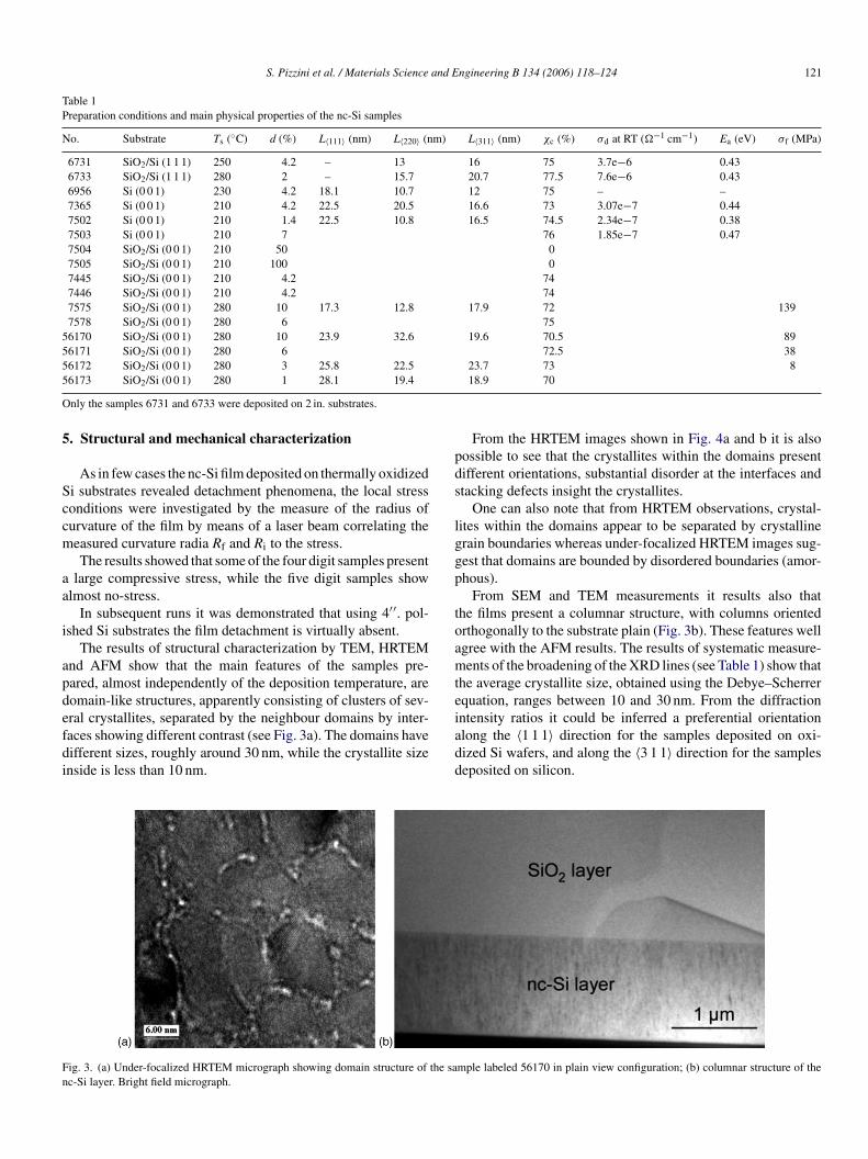
The results of structural characterization by TEM, HRTEMnd AFM show that the main features of the samples pre-ared, almost independently of the deposition temperature, areomain-like structures, apparently consisting of clusters of sev-
ral crystallites, separated by the neighbour domains by inter-aces showing different contrast (see Fig. 3a). The domains haveifferent sizes, roughly around 30 nm, while the crystallite sizenside is less than 10 nm.iadd
ig. 3. (a) Under-focalized HRTEM micrograph showing domain structure of the sac-Si layer. Bright field micrograph.
23.7 73 818.9 70
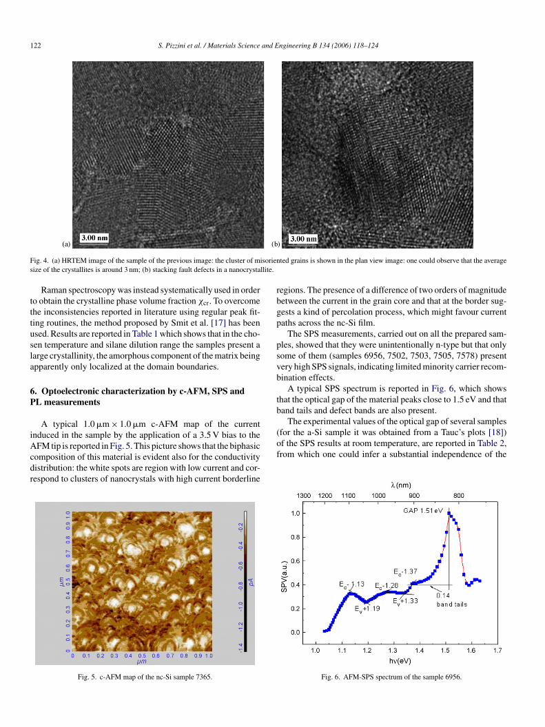
From the HRTEM images shown in Fig. 4a and b it is alsoossible to see that the crystallites within the domains presentifferent orientations, substantial disorder at the interfaces andtacking defects insight the crystallites.
One can also note that from HRTEM observations, crystal-ites within the domains appear to be separated by crystallinerain boundaries whereas under-focalized HRTEM images sug-est that domains are bounded by disordered boundaries (amor-hous).
From SEM and TEM measurements it results also thathe films present a columnar structure, with columns orientedrthogonally to the substrate plain (Fig. 3b). These features wellgree with the AFM results. The results of systematic measure-ents of the broadening of the XRD lines (see Table 1) show that
he average crystallite size, obtained using the Debye–Scherrerquation, ranges between 10 and 30 nm. From the diffraction
ntensity ratios it could be inferred a preferential orientationlong the 〈1 1 1〉 direction for the samples deposited on oxi-ized Si wafers, and along the 〈3 1 1〉 direction for the sampleseposited on silicon.mple labeled 56170 in plain view configuration; (b) columnar structure of the
122 S. Pizzini et al. / Materials Science and Engineering B 134 (2006) 118–124
F soriens llite.
tttusla
6P
iAcdr
rbgp
psvb
tb
(for the a-Si sample it was obtained from a Tauc’s plots [18])
ig. 4. (a) HRTEM image of the sample of the previous image: the cluster of miize of the crystallites is around 3 nm; (b) stacking fault defects in a nanocrysta
Raman spectroscopy was instead systematically used in ordero obtain the crystalline phase volume fraction χcr. To overcomehe inconsistencies reported in literature using regular peak fit-ing routines, the method proposed by Smit et al. [17] has beensed. Results are reported in Table 1 which shows that in the cho-en temperature and silane dilution range the samples present aarge crystallinity, the amorphous component of the matrix beingpparently only localized at the domain boundaries.
. Optoelectronic characterization by c-AFM, SPS andL measurements
A typical 1.0 �m × 1.0 �m c-AFM map of the currentnduced in the sample by the application of a 3.5 V bias to the
FM tip is reported in Fig. 5. This picture shows that the biphasicomposition of this material is evident also for the conductivityistribution: the white spots are region with low current and cor-espond to clusters of nanocrystals with high current borderline
Fig. 5. c-AFM map of the nc-Si sample 7365.
of
ted grains is shown in the plan view image: one could observe that the average
egions. The presence of a difference of two orders of magnitudeetween the current in the grain core and that at the border sug-ests a kind of percolation process, which might favour currentaths across the nc-Si film.
The SPS measurements, carried out on all the prepared sam-les, showed that they were unintentionally n-type but that onlyome of them (samples 6956, 7502, 7503, 7505, 7578) presentery high SPS signals, indicating limited minority carrier recom-ination effects.
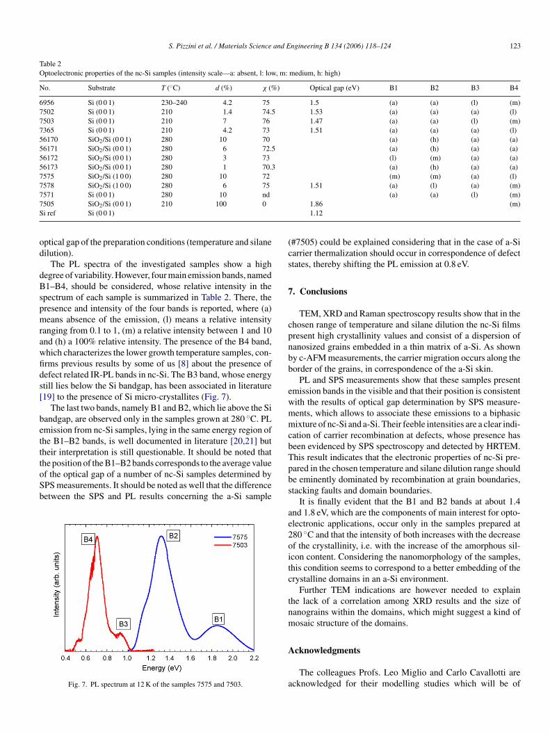
A typical SPS spectrum is reported in Fig. 6, which showshat the optical gap of the material peaks close to 1.5 eV and thatand tails and defect bands are also present.
The experimental values of the optical gap of several samples
f the SPS results at room temperature, are reported in Table 2,rom which one could infer a substantial independence of the
Fig. 6. AFM-SPS spectrum of the sample 6956.
S. Pizzini et al. / Materials Science and Engineering B 134 (2006) 118–124 123
Table 2Optoelectronic properties of the nc-Si samples (intensity scale—a: absent, l: low, m: medium, h: high)
No. Substrate T (◦C) d (%) χ (%) Optical gap (eV) B1 B2 B3 B4
6956 Si (0 0 1) 230–240 4.2 75 1.5 (a) (a) (l) (m)7502 Si (0 0 1) 210 1.4 74.5 1.53 (a) (a) (a) (l)7503 Si (0 0 1) 210 7 76 1.47 (a) (a) (l) (m)7365 Si (0 0 1) 210 4.2 73 1.51 (a) (a) (a) (l)56170 SiO2/Si (0 0 1) 280 10 70 (a) (h) (a) (a)56171 SiO2/Si (0 0 1) 280 6 72.5 (a) (h) (a) (a)56172 SiO2/Si (0 0 1) 280 3 73 (l) (m) (a) (a)56173 SiO2/Si (0 0 1) 280 1 70.3 (a) (h) (a) (a)7575 SiO2/Si (1 0 0) 280 10 72 (m) (m) (a) (l)7578 SiO2/Si (1 0 0) 280 6 75 1.51 (a) (l) (a) (m)77S
od
dBspmrawfids[
betttoSb
(cs
7
cpnbb
ewmmcbT
571 Si (0 0 1) 280 10 nd505 SiO2/Si (0 0 1) 210 100 0i ref Si (0 0 1)
ptical gap of the preparation conditions (temperature and silaneilution).
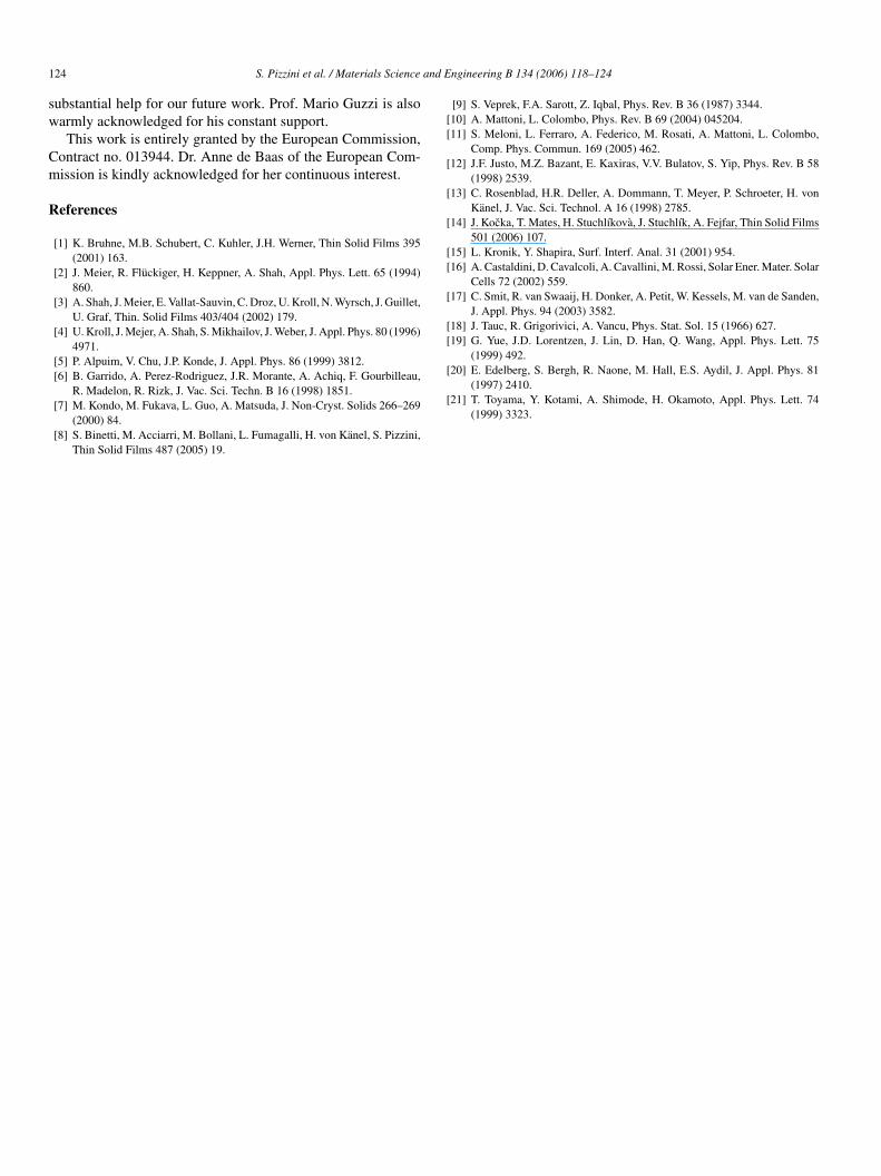
The PL spectra of the investigated samples show a highegree of variability. However, four main emission bands, named1–B4, should be considered, whose relative intensity in the
pectrum of each sample is summarized in Table 2. There, theresence and intensity of the four bands is reported, where (a)eans absence of the emission, (l) means a relative intensity
anging from 0.1 to 1, (m) a relative intensity between 1 and 10nd (h) a 100% relative intensity. The presence of the B4 band,hich characterizes the lower growth temperature samples, con-rms previous results by some of us [8] about the presence ofefect related IR-PL bands in nc-Si. The B3 band, whose energytill lies below the Si bandgap, has been associated in literature19] to the presence of Si micro-crystallites (Fig. 7).
The last two bands, namely B1 and B2, which lie above the Siandgap, are observed only in the samples grown at 280 ◦C. PLmission from nc-Si samples, lying in the same energy region ofhe B1–B2 bands, is well documented in literature [20,21] butheir interpretation is still questionable. It should be noted thathe position of the B1–B2 bands corresponds to the average value
f the optical gap of a number of nc-Si samples determined byPS measurements. It should be noted as well that the differenceetween the SPS and PL results concerning the a-Si sampleFig. 7. PL spectrum at 12 K of the samples 7575 and 7503.
pbs
ae2oitc
tnm
A
a
(a) (a) (l) (m)1.86 (m)1.12
#7505) could be explained considering that in the case of a-Siarrier thermalization should occur in correspondence of defecttates, thereby shifting the PL emission at 0.8 eV.
. Conclusions
TEM, XRD and Raman spectroscopy results show that in thehosen range of temperature and silane dilution the nc-Si filmsresent high crystallinity values and consist of a dispersion ofanosized grains embedded in a thin matrix of a-Si. As showny c-AFM measurements, the carrier migration occurs along theorder of the grains, in correspondence of the a-Si skin.
PL and SPS measurements show that these samples presentmission bands in the visible and that their position is consistentith the results of optical gap determination by SPS measure-ents, which allows to associate these emissions to a biphasicixture of nc-Si and a-Si. Their feeble intensities are a clear indi-
ation of carrier recombination at defects, whose presence haseen evidenced by SPS spectroscopy and detected by HRTEM.his result indicates that the electronic properties of nc-Si pre-ared in the chosen temperature and silane dilution range shoulde eminently dominated by recombination at grain boundaries,tacking faults and domain boundaries.
It is finally evident that the B1 and B2 bands at about 1.4nd 1.8 eV, which are the components of main interest for opto-lectronic applications, occur only in the samples prepared at80 ◦C and that the intensity of both increases with the decreasef the crystallinity, i.e. with the increase of the amorphous sil-con content. Considering the nanomorphology of the samples,his condition seems to correspond to a better embedding of therystalline domains in an a-Si environment.
Further TEM indications are however needed to explainhe lack of a correlation among XRD results and the size ofanograins within the domains, which might suggest a kind ofosaic structure of the domains.
cknowledgments
The colleagues Profs. Leo Miglio and Carlo Cavallotti arecknowledged for their modelling studies which will be of
1 and E
sw
Cm
R
[[
[
[
[
[[
[
[[
(1999) 492.[20] E. Edelberg, S. Bergh, R. Naone, M. Hall, E.S. Aydil, J. Appl. Phys. 81
(1997) 2410.
24 S. Pizzini et al. / Materials Science
ubstantial help for our future work. Prof. Mario Guzzi is alsoarmly acknowledged for his constant support.This work is entirely granted by the European Commission,
ontract no. 013944. Dr. Anne de Baas of the European Com-ission is kindly acknowledged for her continuous interest.
eferences
[1] K. Bruhne, M.B. Schubert, C. Kuhler, J.H. Werner, Thin Solid Films 395(2001) 163.
[2] J. Meier, R. Fluckiger, H. Keppner, A. Shah, Appl. Phys. Lett. 65 (1994)860.
[3] A. Shah, J. Meier, E. Vallat-Sauvin, C. Droz, U. Kroll, N. Wyrsch, J. Guillet,U. Graf, Thin. Solid Films 403/404 (2002) 179.
[4] U. Kroll, J. Mejer, A. Shah, S. Mikhailov, J. Weber, J. Appl. Phys. 80 (1996)4971.
[5] P. Alpuim, V. Chu, J.P. Konde, J. Appl. Phys. 86 (1999) 3812.[6] B. Garrido, A. Perez-Rodriguez, J.R. Morante, A. Achiq, F. Gourbilleau,
R. Madelon, R. Rizk, J. Vac. Sci. Techn. B 16 (1998) 1851.[7] M. Kondo, M. Fukava, L. Guo, A. Matsuda, J. Non-Cryst. Solids 266–269
(2000) 84.[8] S. Binetti, M. Acciarri, M. Bollani, L. Fumagalli, H. von Kanel, S. Pizzini,
Thin Solid Films 487 (2005) 19.
[
ngineering B 134 (2006) 118–124
[9] S. Veprek, F.A. Sarott, Z. Iqbal, Phys. Rev. B 36 (1987) 3344.10] A. Mattoni, L. Colombo, Phys. Rev. B 69 (2004) 045204.11] S. Meloni, L. Ferraro, A. Federico, M. Rosati, A. Mattoni, L. Colombo,
Comp. Phys. Commun. 169 (2005) 462.12] J.F. Justo, M.Z. Bazant, E. Kaxiras, V.V. Bulatov, S. Yip, Phys. Rev. B 58
(1998) 2539.13] C. Rosenblad, H.R. Deller, A. Dommann, T. Meyer, P. Schroeter, H. von
Kanel, J. Vac. Sci. Technol. A 16 (1998) 2785.14] J. Kocka, T. Mates, H. Stuchlıkova, J. Stuchlık, A. Fejfar, Thin Solid Films
501 (2006) 107.15] L. Kronik, Y. Shapira, Surf. Interf. Anal. 31 (2001) 954.16] A. Castaldini, D. Cavalcoli, A. Cavallini, M. Rossi, Solar Ener. Mater. Solar
Cells 72 (2002) 559.17] C. Smit, R. van Swaaij, H. Donker, A. Petit, W. Kessels, M. van de Sanden,
J. Appl. Phys. 94 (2003) 3582.18] J. Tauc, R. Grigorivici, A. Vancu, Phys. Stat. Sol. 15 (1966) 627.19] G. Yue, J.D. Lorentzen, J. Lin, D. Han, Q. Wang, Appl. Phys. Lett. 75
21] T. Toyama, Y. Kotami, A. Shimode, H. Okamoto, Appl. Phys. Lett. 74(1999) 3323.
Related Documents